EP2664976A2 - Power management unit including a signal protection circuit - Google Patents
Power management unit including a signal protection circuit Download PDFInfo
- Publication number
- EP2664976A2 EP2664976A2 EP12008558.4A EP12008558A EP2664976A2 EP 2664976 A2 EP2664976 A2 EP 2664976A2 EP 12008558 A EP12008558 A EP 12008558A EP 2664976 A2 EP2664976 A2 EP 2664976A2
- Authority
- EP
- European Patent Office
- Prior art keywords
- gain control
- pmu
- protection circuit
- control block
- oscillator
- Prior art date
- Legal status (The legal status is an assumption and is not a legal conclusion. Google has not performed a legal analysis and makes no representation as to the accuracy of the status listed.)
- Granted
Links
Images


Classifications
-
- G—PHYSICS
- G06—COMPUTING OR CALCULATING; COUNTING
- G06F—ELECTRIC DIGITAL DATA PROCESSING
- G06F1/00—Details not covered by groups G06F3/00 - G06F13/00 and G06F21/00
- G06F1/04—Generating or distributing clock signals or signals derived directly therefrom
-
- G—PHYSICS
- G06—COMPUTING OR CALCULATING; COUNTING
- G06F—ELECTRIC DIGITAL DATA PROCESSING
- G06F1/00—Details not covered by groups G06F3/00 - G06F13/00 and G06F21/00
- G06F1/26—Power supply means, e.g. regulation thereof
- G06F1/263—Arrangements for using multiple switchable power supplies, e.g. battery and AC
-
- G—PHYSICS
- G06—COMPUTING OR CALCULATING; COUNTING
- G06F—ELECTRIC DIGITAL DATA PROCESSING
- G06F1/00—Details not covered by groups G06F3/00 - G06F13/00 and G06F21/00
- G06F1/26—Power supply means, e.g. regulation thereof
- G06F1/32—Means for saving power
- G06F1/3203—Power management, i.e. event-based initiation of a power-saving mode
- G06F1/3234—Power saving characterised by the action undertaken
- G06F1/324—Power saving characterised by the action undertaken by lowering clock frequency
-
- H—ELECTRICITY
- H03—ELECTRONIC CIRCUITRY
- H03B—GENERATION OF OSCILLATIONS, DIRECTLY OR BY FREQUENCY-CHANGING, BY CIRCUITS EMPLOYING ACTIVE ELEMENTS WHICH OPERATE IN A NON-SWITCHING MANNER; GENERATION OF NOISE BY SUCH CIRCUITS
- H03B5/00—Generation of oscillations using amplifier with regenerative feedback from output to input
- H03B5/30—Generation of oscillations using amplifier with regenerative feedback from output to input with frequency-determining element being electromechanical resonator
- H03B5/32—Generation of oscillations using amplifier with regenerative feedback from output to input with frequency-determining element being electromechanical resonator being a piezoelectric resonator
- H03B5/36—Generation of oscillations using amplifier with regenerative feedback from output to input with frequency-determining element being electromechanical resonator being a piezoelectric resonator active element in amplifier being semiconductor device
- H03B5/364—Generation of oscillations using amplifier with regenerative feedback from output to input with frequency-determining element being electromechanical resonator being a piezoelectric resonator active element in amplifier being semiconductor device the amplifier comprising field effect transistors
-
- H—ELECTRICITY
- H03—ELECTRONIC CIRCUITRY
- H03L—AUTOMATIC CONTROL, STARTING, SYNCHRONISATION OR STABILISATION OF GENERATORS OF ELECTRONIC OSCILLATIONS OR PULSES
- H03L5/00—Automatic control of voltage, current, or power
-
- H—ELECTRICITY
- H03—ELECTRONIC CIRCUITRY
- H03L—AUTOMATIC CONTROL, STARTING, SYNCHRONISATION OR STABILISATION OF GENERATORS OF ELECTRONIC OSCILLATIONS OR PULSES
- H03L7/00—Automatic control of frequency or phase; Synchronisation
-
- H—ELECTRICITY
- H03—ELECTRONIC CIRCUITRY
- H03B—GENERATION OF OSCILLATIONS, DIRECTLY OR BY FREQUENCY-CHANGING, BY CIRCUITS EMPLOYING ACTIVE ELEMENTS WHICH OPERATE IN A NON-SWITCHING MANNER; GENERATION OF NOISE BY SUCH CIRCUITS
- H03B2200/00—Indexing scheme relating to details of oscillators covered by H03B
- H03B2200/003—Circuit elements of oscillators
- H03B2200/0038—Circuit elements of oscillators including a current mirror
-
- H—ELECTRICITY
- H03—ELECTRONIC CIRCUITRY
- H03B—GENERATION OF OSCILLATIONS, DIRECTLY OR BY FREQUENCY-CHANGING, BY CIRCUITS EMPLOYING ACTIVE ELEMENTS WHICH OPERATE IN A NON-SWITCHING MANNER; GENERATION OF NOISE BY SUCH CIRCUITS
- H03B2200/00—Indexing scheme relating to details of oscillators covered by H03B
- H03B2200/003—Circuit elements of oscillators
- H03B2200/0046—Circuit elements of oscillators including measures to switch the gain of an amplifier
-
- H—ELECTRICITY
- H03—ELECTRONIC CIRCUITRY
- H03B—GENERATION OF OSCILLATIONS, DIRECTLY OR BY FREQUENCY-CHANGING, BY CIRCUITS EMPLOYING ACTIVE ELEMENTS WHICH OPERATE IN A NON-SWITCHING MANNER; GENERATION OF NOISE BY SUCH CIRCUITS
- H03B2200/00—Indexing scheme relating to details of oscillators covered by H03B
- H03B2200/006—Functional aspects of oscillators
- H03B2200/0082—Lowering the supply voltage and saving power
-
- Y—GENERAL TAGGING OF NEW TECHNOLOGICAL DEVELOPMENTS; GENERAL TAGGING OF CROSS-SECTIONAL TECHNOLOGIES SPANNING OVER SEVERAL SECTIONS OF THE IPC; TECHNICAL SUBJECTS COVERED BY FORMER USPC CROSS-REFERENCE ART COLLECTIONS [XRACs] AND DIGESTS
- Y02—TECHNOLOGIES OR APPLICATIONS FOR MITIGATION OR ADAPTATION AGAINST CLIMATE CHANGE
- Y02D—CLIMATE CHANGE MITIGATION TECHNOLOGIES IN INFORMATION AND COMMUNICATION TECHNOLOGIES [ICT], I.E. INFORMATION AND COMMUNICATION TECHNOLOGIES AIMING AT THE REDUCTION OF THEIR OWN ENERGY USE
- Y02D10/00—Energy efficient computing, e.g. low power processors, power management or thermal management
Definitions
- Mobile communication devices or "mobile devices" are widely used and relied upon for business, personal, and emergency communications. As mobile devices have become more powerful and sophisticated, battery life has become a greater user preoccupation. For example, some modem smartphones may require recharging more than once a day.
- a mobile device user may prefer to simply remove and replace a spent or depleted battery.
- Attempts to accommodate battery replacement include preserving register values of the mobile device by making a transition into a low power standby mode during a pre-determined time interval. It is desirable that the internal clock as well as register values of mobile devices be preserved during an allowed time window for battery replacement.
- the present disclosure is directed to a power management unit including a signal protection circuit, as shown in and/or described in connection with at least one of the figures, and as set forth more completely in the claims.
- a power management unit that comprises:
- said oscillator is a crystal oscillator.
- said gain control block comprises an automatic gain control (AGC) block.
- AGC automatic gain control
- said signal protection circuit comprises a digitally controlled variable capacitor coupled between said input of said gain control block and ground.
- said signal protection circuit is configured to limit a rate of change of a gain control block input signal received by said input of said gain control block during said transition to said standby mode.
- said rate of change of said gain control block input signal is limited based on a time constant of said oscillator.
- a mobile device that comprises:
- said signal protection circuit is implemented as part of a power management unit (PMU) of said mobile device.
- PMU power management unit
- said mobile device comprises a mobile phone.
- said oscillator is a crystal oscillator.
- said gain control block comprises an automatic gain control (AGC) block.
- AGC automatic gain control
- said signal protection circuit comprises a digitally controlled variable capacitor coupled between said input of said gain control block and ground.
- said signal protection circuit is configured to limit a rate of change of a gain control block input signal received by said input of said gain control block during said transition to said standby mode.
- said rate of change of said gain control block input signal is limited based on a time constant of said oscillator.
- a power management unit that comprises:
- said oscillator is a crystal oscillator.
- said signal protection circuit comprises a digitally controlled variable capacitor coupled between said input of said AGC block and ground.
- said signal protection circuit comprises a digitally controlled variable capacitor coupled between said input of said AGC block and ground.
- said rate of change of said AGC block input signal is limited based on a time constant of said oscillator.
- said PMU is implemented as part of a wireless transceiver.
- FIG 1 shows a block diagram of a mobile device 100 including an exemplary power management unit (PMU) 120, according to one implementation.
- the PMU 120 is implemented as part of a wireless transceiver 102 of the mobile device 100.
- the wireless transceiver 102 includes a receiver 105, a transmitter 106, and an oscillator 110.
- the mobile device 100 also includes an antenna 101, a low-noise amplifier (LNA) block 103 coupling the antenna 101 to the receiver 105, and a power amplifier (PA) block 104 coupling the antenna 101 to the transmitter 106.
- LNA low-noise amplifier
- PA power amplifier
- the receiver 105 and the transmitter 106 may be selectably coupled to the antenna 101 using duplexer 107, as shown in Figure 1 .
- the mobile device 100 is powered using a battery 108, which may be a rechargeable and removable/replaceable battery serving as the principle power source for the mobile device 100.
- the receiver 105 typically includes mixer circuitry, as well as one or more filtering stages and a digital signal processing (DSP) block.
- the transmitter 106 will typically include a DSP block and transmit chain processing stages configured to provide preamplification gain control for a transmit signal.
- the mobile device 100 may utilize a transmit/receive (T/R) switch (not shown in Figure 1 ) in addition to, or in place of, the duplexer 107.
- the mobile device 100 may be implemented as a smartphone, cell phone, tablet computer, or an e-book reader.
- Other exemplary implementations for the mobile device 100 include a digital media player, wireless gaming console, or any other kind of system utilizing a wireless transceiver in modem electronics applications.
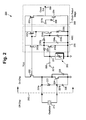
- FIG 2 shows a more detailed diagram of a portion of a PMU 220 including an exemplary implementation of a signal protection circuit 260.
- the PMU 220 is implemented as an integrated circuit (IC) coupled to an off-chip oscillator 210 at the PMU inputs 221a and 221b.
- the oscillator 210 and the PMU 220 correspond respectively to the oscillator 110 and the PMU 120, in Figure 1 .
- the oscillator 210 and the PMU 220 may be implemented as part of a mobile device corresponding to the mobile device 100. It is noted that portions of the PMU 220 not represented in Figure 2 are coupled to a mobile device battery, corresponding to the coupling of the PMU 120 and the battery 108, as shown by Figure 1 .
- the oscillator 210 may be a crystal oscillator, such as a crystal oscillator having a base frequency of approximatly 32,768 hertz (Hz), or a lower or higher frequency.
- the oscillator 210 may be a crystal oscillator producing a higher frequency signal, such as an approximatly 1 MHz, 10 MHz, or 100 MHz signal.
- the oscillator 210 may be a non-crystal oscillator capable of producing a high frequency signal up to approximatly 10 GHz, or higher. Examples of non-crystal osciilators include LC oscillators, coaxial resonator oscillators, and dielectric resonator oscillators.
- the oscillator 210 may be taken on-chip by the IC including the PMU 220.
- the PMU 220 includes transistors 222 and 224, a resistor 223, and capacitors 226 and 228 implemented to drive the oscillator 210.
- the oscillator 210 produces a substantially pure oscillator signal that is taken on-chip to the PMU 220 by the input 221b.
- the PMU 220 also includes a gain control block 230, a clock output stage 250, and a signal protection circuit 260 coupled to an input 231 of the gain control block 230. It is noted that each of the gain control block 230, the clock output stage 250, and the signal protection circuit 260 are also coupled to the input 22 1 b receiving the oscillator signal.
- the gain control block 230 includes transistors 232a and 232b, transistors 234a and 234b, resistors 235, 236a, and 236b, and capacitors 238a and 238b.
- the input 231 of the gain control block 230 is coupled to the signal protection circuit 260.
- the input 231 is coupled to the resistor 235 of the gain control block 230, to a gate of the transistor 234a of the gain control block 230, and through a capacitor 222 to the input 221b.
- the clock output stage 250 includes transistors 252 and 254, capacitor 258, and clock output 259. As shown in Figure 2 , the input 221b to the PMU 220 drives a gate of the transistor 254 through the capacitor 258, to produce the clock output 259. It is noted that a current flowing through each of the transistors 222, 232a, and 252 mirror a current flowing through the transitor 232b. As a result, the current flowing through the transistor 232b can control the mirrored currents flowing through the transistors 222 and 252.
- the gain control block 230 is configured to control the oscillator 210.
- the gain control block 230 which is depicted as an automatic gain control (AGC) block in Figure 2 , is also configured to control the clock output stage 250.
- the signal protection circuit 260 is coupled to an input 231 of the gain control block 230 and is configured to digitally control the gain control block 230.
- the signal protection circuit 260 is configured to preserve clock signals produced by the clock output stage 250 during a transition to a standby mode.
- a transition to a standby mode may correspond to any transition from a normal operating mode to a low power mode. Examples of a standby mode include a low or ultra-low power mode, an emergency power conservation mode, and a real-time clock (RTC) mode.
- RTC real-time clock
- the standby mode may be a power conservation mode triggered by removal of the principle battery used to power a mobile device.
- the standby mode may correspond to a low power or ultra-low power mode initiated by the PMU 120 in response to removal of the battery 108. Removal of the battery 108 may occur due to substantial depletion of the battery 108, and may presage insertion of a substantially charged replacement battery as a substitute for the battery 108.
- the PMU 120 may be configured to transition the mobile device 100 into a low power or ultra-low power standby mode in order to maintain register values and/or clock functionality when the battery 108 is removed.
- the standby mode may be implemented to maintain the register values during a pre-determined time interval for replacing the battery 108, such as an approximately sixty (60) second time interval.
- the signal protection circuit is configured to preserve clock signals produced by a clock output stage, such as clock output stage 250, in Figure 2 , during the pre-determined time interval for replacing the battery 108.
- the signal protection circuit 260 may include a variable capacitor, such as a digitally controlled variable capacitor, coupled between the input 231 of the gain control block 230 and ground.
- the signal protection circuit 260 is configured to limit a rate of change of a gain control block input signal received by the input 231 during the transition to the standby mode.
- the limitation imposed on the rate of change of the gain control block input signal is based on the time constant of the oscillator 110/210.
- an oscillator time constant is the time required for the amplitude of oscillations produced by an un-driven oscillator to decay to substantially 1/e its initial value (i.e., approximately thirty-seven percent of its initial value).
- Figure 3 shows an exemplary implementation of a signal protection circuit 360 for use in the PMU 120/220.
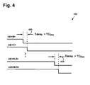
- Figure 4 shows an exemplary timing diagram 460 corresponding to preservation of clock signals during a transition to a standby mode.
- Figure 3 shows a block diagram of signal protection circuit 360 implemented as a digitally controlled variable capacitor including a network of switchable unit capacitor branches 361 arranged in parallel.
- Signal protection circuit 360 corresponds to signal protection circuit 260, in Figure 2 .
- signal protection circuit 360 includes a number "N" of the parallel switchable unit capacitor branches 361.
- Each of the branches 361 includes a respective unit capacitor 364 (0) ,364 (1) ,..., 364 (N-2) , 364 (N-1) (hereinafter “unit capacitors 364 (0) -364 (N-1) ").
- each of the branches 361 includes a respective switch 366 (0) ,366 (1) ,..., 366 (N-2) , 366 (N-1) (hereinafter “switches 366 (0) -366 (N-1) ").
- the switches 366 (0) -366 (N-1) may be used for switching the respective unit capacitors 364 (0) -364 (N-1) into and out of the collective capacitance produced by the network of branches 361.
- the signal protection circuit 360 also includes a counter 362 configured to provide control signals ctrl ⁇ 0>, ctrl ⁇ 1>, ..., ctrl ⁇ N-2>, ctrl ⁇ N-1> (hereinafter "control signals ctrl ⁇ 0>-ctrl ⁇ N-1>") for selectably turning the respective switches 366 (0) -366 (N-1) OFF or ON. Also shown in Figure 3 is an input 331, corresponding to the input 231 of the gain control block 230, in Figure 2 .
- Figure 4 shows timing diagram 460 corresponding to control of the switches 366 (0) -366 (N-1) , in Figure 3 , by the counter 362.
- the counter 362 can be configured to gradually turn the switches 366 (0) -366 (N-1) OFF, utilizing a delay 468 between each of the successive control signals ctrl ⁇ 0>-ctrl ⁇ N-1>.
- the delay 468 is selected so as to be greater than the time constant of the oscillator 110/210.
- the exemplary signal protection circuit 360 shown in Figure 3 , can enable a digitally controlled and graduated transition of the capacitance of the network of branches 361.
- Such a transition can correspond to a transition to a standby mode by the PMU 120/220.
- Use of the delay 468 selected to be greater than the time constant of the oscillator 110/220 preserves clock signals produced by the clock output stage 250 during the transition to the standby mode.
- the PMU 120/220 may be configured to keep the mobile device 100 operational using a relatively higher current to ensure good jitter performance.
- the amplitude of the gain control block input signal is typically attenuated with respect to the oscillator signal received at the PMU input 221b. That attenuation of the signal at input 231 is produced by the voltage divider formed by capacitor 222 and the capacitance provided by the signal protection circuit 260. If, for example, the capacitance of the capacitor 222 is C and the normal operating mode capacitance of the signal protection circuit 260 is 9C, the oscillator signal at the input 221b is reduced by approximately tenfold (1/10) at the input 231.
- the gain control block 230 is configured to respond to changes in the gain control block input signal so as to stabilize the performance of the oscillator 210.
- a large and/or sudden increase in the gain control block input signal can be expected to trigger a significant corrective response by the gain control block 230. If not properly mitigated, the corrective response by the gain control circuit 230 can have potentially undesirable consequences for the performance of the clock output stage 250.
- the capacitor 222 has capacitance C and the signal protection circuit 260 has a normal operating mode capacitance of 9C.
- the abrupt switching out of the capacitance provided by the signal protection circuit 260 would cause the gain control block input signal at the input 231 to increase by a factor of approximately ten.
- the gain control block input signal received at input 231 drives the gate of the transistor 234a.
- the sudden increase in the amplitude of the driving signal for the transistor 234a will pull the gate of the transistor 234b LOW, turning the transistor 234b OFF. That, in turn, causes the transistor 232b, implemented as a PMOS transistor, to turn OFF as well.
- the transistors 222, 232a, and 252 also implemented as PMOS transistors, mirror the transistor 232b, the transistors 222, 232a, and 252 are also turned OFF.
- the clock output stage 250 can be temporarily disabled as a result of an abrupt increase in the gain control block input signal received at the input 231.
- signal protection circuit 260 limits the rate of change of the gain control block input signal. Such a result can be accomplished in a variety of ways. In one implementation, the rate of change of the gain control input signal is limited, and the clock signals produced by the clock output stage 250 are preserved, by gradually reducing the collective capacitance of the signal protection circuit 360.
- a shutdown control signal ctrl ⁇ 0> causes the unit capacitor 364 (0) to be switched out of the capacitor network of the signal protection circuit 360 by its respective switch 366 (0) .
- the control signal ctrl ⁇ 0> results in an incremental decrease in the capacitance provided by the signal protection circuit 360. That incremental reduction in the capacitance of the signal protection circuit 360 causes a corresponding incremental increase in the gain control block input signal at the input 231/331.
- the shutdown control signal ctrl ⁇ 1> causes the unit capacitor 364 (1) to be switched out of the capacitor network of the signal protection circuit 360 as well. Thereafter, the remaining unit capacitors are switched out one-by-one after additional respective delays 468. After “N” such delays 468, all of the unit capacitors 364 (0) -364 (N-1) are switched out and the transition to the standby mode is complete.
- the transition to the standby mode can be optimized so as to occur as rapidly as possible while preserving the clock signals produced by the clock output stage 250.
- One possible constraint on these parameters is introduced by the time constant of the oscillator 110/210. Consequently, in one implementation, the delay 468 is selected such that it is greater than the time constant of the oscillator 110/210.
- the signal protection circuit 260/360 can also be utilized to produce a graduated transition from the standby mode to the normal operating mode, if desired.
- one or more of the unit capacitors 364 (0) -364 (N-1) may be concurrently switched in to the capacitor network shown in Figure 3 during a transition to the normal operating mode.
- Such a transition may be governed by delay 468, or by another delay interval optimized for a return to higher current operation.
- it may be desirable to return to the normal operating mode without utilizing a delay such as the delay 468.
- all or substantially all of the unit capacitors 364 (0) -364 (N-1) may be switched into the signal protection circuit 360 concurrently.
- a user may simply remove and replace a spent or depleted battery. Such replacement can be accomplished without erasing register values, such as alarm or timer settings. Moreover, clock signals produced by an internal clock of the mobile device are not lost during the transition to the low power standby mode.
- the present application discloses a signal protection circuit configured to preserve clock signals during a transition to a standby mode.
- a signal protection circuit configured to preserve clock signals during a transition to a standby mode.
- implementations of the present solution enable a graduated transition from a normal operating mode to the standby mode.
- implementations of the present solution prevent a clock output stage controlled by the gain control loop from being disabled during the transition to the standby mode.
- the signal protection circuit disclosed by the present application enables reliable and continuous clock functionality during the transition to the standby mode.
Landscapes
- Engineering & Computer Science (AREA)
- Theoretical Computer Science (AREA)
- Physics & Mathematics (AREA)
- General Engineering & Computer Science (AREA)
- General Physics & Mathematics (AREA)
- Power Engineering (AREA)
- Telephone Function (AREA)
- Transceivers (AREA)
- Mobile Radio Communication Systems (AREA)
- Transmitters (AREA)
- Circuits Of Receivers In General (AREA)
Abstract
Description
- Mobile communication devices, or "mobile devices", are widely used and relied upon for business, personal, and emergency communications. As mobile devices have become more powerful and sophisticated, battery life has become a greater user preoccupation. For example, some modem smartphones may require recharging more than once a day.
- Rather than suffer the inconvenience imposed by the need for frequent recharging, a mobile device user may prefer to simply remove and replace a spent or depleted battery. Attempts to accommodate battery replacement include preserving register values of the mobile device by making a transition into a low power standby mode during a pre-determined time interval. It is desirable that the internal clock as well as register values of mobile devices be preserved during an allowed time window for battery replacement.
- The present disclosure is directed to a power management unit including a signal protection circuit, as shown in and/or described in connection with at least one of the figures, and as set forth more completely in the claims.
-
-
Figure 1 shows a block diagram of a mobile device including an exemplary power management unit (PMU), according to one implementation. -
Figure 2 shows a more detailed diagram of a portion of a PMU including an exemplary implementation of a signal protection circuit. -
Figure 3 shows an exemplary implementation of a signal protection circuit for use in a PMU. -
Figure 4 shows an exemplary timing diagram corresponding to preservation of clock signals during a transition to a standby mode. - The following description contains specific information pertaining to implementations in the present disclosure.
- According to one aspect of the invention, a power management unit (PMU) is provided that comprises:
- a gain control block configured to control an oscillator coupled to said PMU;
- said gain control block configured to control a clock output stage;
- a signal protection circuit coupled to an input of said gain control block;
- said signal protection circuit configured to preserve clock signals produced by said clock output stage during a transition to a standby mode.
- Advantageously, said oscillator is a crystal oscillator.
- Advantageously, said gain control block comprises an automatic gain control (AGC) block.
- Advantageously, said signal protection circuit comprises a digitally controlled variable capacitor coupled between said input of said gain control block and ground.
- Advantageously, said signal protection circuit is configured to limit a rate of change of a gain control block input signal received by said input of said gain control block during said transition to said standby mode.
- Advantageously, said rate of change of said gain control block input signal is limited based on a time constant of said oscillator.
- According to another aspect of the invention, a mobile device is provided that comprises:
- a battery;
- a gain control block configured to control an oscillator;
- said gain control block configured to control a clock output stage;
- a signal protection circuit coupled to an input of said gain control block;
- said signal protection circuit configured to preserve clock signals produced by said clock output stage during a pre-determined time interval for replacing said battery.
- Advantageously, said signal protection circuit is implemented as part of a power management unit (PMU) of said mobile device.
- Advantageously, said mobile device comprises a mobile phone.
- Advantageously, said oscillator is a crystal oscillator.
- Advantageously, said gain control block comprises an automatic gain control (AGC) block.
- Advantageously, said signal protection circuit comprises a digitally controlled variable capacitor coupled between said input of said gain control block and ground.
- Advantageously, said signal protection circuit is configured to limit a rate of change of a gain control block input signal received by said input of said gain control block during said transition to said standby mode.
- Advantageously, said rate of change of said gain control block input signal is limited based on a time constant of said oscillator.
- According to another aspect of the invention, a power management unit (PMU) is provided that comprises:
- an automatic gain control (AGC) block configured to control an oscillator coupled to said PMU;
- said AGC block configured to control a clock output stage;
- a signal protection circuit configured to limit a rate of change of an AGC block input signal received by an input of said AGC block during a transition to a standby mode.
- Advantageously, said oscillator is a crystal oscillator.
- Advantageously, said signal protection circuit comprises a digitally controlled variable capacitor coupled between said input of said AGC block and ground.
- Advantageously, said signal protection circuit comprises a digitally controlled variable capacitor coupled between said input of said AGC block and ground.
- Advantageously, said rate of change of said AGC block input signal is limited based on a time constant of said oscillator.
- Advantageously, said PMU is implemented as part of a wireless transceiver.
- The drawings in the present application and their accompanying detailed description are directed to merely exemplary implementations. Unless noted otherwise, like or corresponding elements among the figures may be indicated by like or corresponding reference numerals. Moreover, the drawings and illustrations in the present application are generally not to scale, and are not intended to correspond to actual relative dimensions.
-
Figure 1 shows a block diagram of amobile device 100 including an exemplary power management unit (PMU) 120, according to one implementation. The PMU 120 is implemented as part of awireless transceiver 102 of themobile device 100. In addition to thePMU 120, thewireless transceiver 102 includes areceiver 105, atransmitter 106, and anoscillator 110. Themobile device 100 also includes anantenna 101, a low-noise amplifier (LNA)block 103 coupling theantenna 101 to thereceiver 105, and a power amplifier (PA)block 104 coupling theantenna 101 to thetransmitter 106. Thereceiver 105 and thetransmitter 106 may be selectably coupled to theantenna 101 usingduplexer 107, as shown inFigure 1 . Themobile device 100 is powered using abattery 108, which may be a rechargeable and removable/replaceable battery serving as the principle power source for themobile device 100. - It is noted that although not explicitly shown as such in
Figure 1 , thereceiver 105 typically includes mixer circuitry, as well as one or more filtering stages and a digital signal processing (DSP) block. It is further noted that thetransmitter 106 will typically include a DSP block and transmit chain processing stages configured to provide preamplification gain control for a transmit signal. Moreover, in other implementations, themobile device 100 may utilize a transmit/receive (T/R) switch (not shown inFigure 1 ) in addition to, or in place of, theduplexer 107. Themobile device 100 may be implemented as a smartphone, cell phone, tablet computer, or an e-book reader. Other exemplary implementations for themobile device 100 include a digital media player, wireless gaming console, or any other kind of system utilizing a wireless transceiver in modem electronics applications. -
Figure 2 shows a more detailed diagram of a portion of aPMU 220 including an exemplary implementation of asignal protection circuit 260. As indicated bychip boundary 212, thePMU 220 is implemented as an integrated circuit (IC) coupled to an off-chip oscillator 210 at thePMU inputs oscillator 210 and thePMU 220 correspond respectively to theoscillator 110 and thePMU 120, inFigure 1 . In other words, theoscillator 210 and thePMU 220 may be implemented as part of a mobile device corresponding to themobile device 100. It is noted that portions of thePMU 220 not represented inFigure 2 are coupled to a mobile device battery, corresponding to the coupling of thePMU 120 and thebattery 108, as shown byFigure 1 . - The
oscillator 210 may be a crystal oscillator, such as a crystal oscillator having a base frequency of approximatly 32,768 hertz (Hz), or a lower or higher frequency. For example, theoscillator 210 may be a crystal oscillator producing a higher frequency signal, such as anapproximatly 1 MHz, 10 MHz, or 100 MHz signal. In still other implementations, theoscillator 210 may be a non-crystal oscillator capable of producing a high frequency signal up to approximatly 10 GHz, or higher. Examples of non-crystal osciilators include LC oscillators, coaxial resonator oscillators, and dielectric resonator oscillators. Moreover, when implemented as a non-crystal oscillator, theoscillator 210 may be taken on-chip by the IC including thePMU 220. - The
PMU 220 includestransistors resistor 223, andcapacitors oscillator 210. In response, theoscillator 210 produces a substantially pure oscillator signal that is taken on-chip to thePMU 220 by theinput 221b. ThePMU 220 also includes again control block 230, a clock output stage 250, and asignal protection circuit 260 coupled to aninput 231 of thegain control block 230. It is noted that each of thegain control block 230, the clock output stage 250, and thesignal protection circuit 260 are also coupled to the input 22 1 b receiving the oscillator signal. - The
gain control block 230 includestransistors transistors 234a and 234b,resistors capacitors input 231 of thegain control block 230 is coupled to thesignal protection circuit 260. In addition, theinput 231 is coupled to theresistor 235 of thegain control block 230, to a gate of the transistor 234a of thegain control block 230, and through acapacitor 222 to theinput 221b. - The clock output stage 250 includes
transistors capacitor 258, andclock output 259. As shown inFigure 2 , theinput 221b to thePMU 220 drives a gate of thetransistor 254 through thecapacitor 258, to produce theclock output 259. It is noted that a current flowing through each of thetransistors transistor 232b can control the mirrored currents flowing through thetransistors - Thus, the
gain control block 230 is configured to control theoscillator 210. Thegain control block 230, which is depicted as an automatic gain control (AGC) block inFigure 2 , is also configured to control the clock output stage 250. Thesignal protection circuit 260 is coupled to aninput 231 of thegain control block 230 and is configured to digitally control thegain control block 230. As a result, thesignal protection circuit 260 is configured to preserve clock signals produced by the clock output stage 250 during a transition to a standby mode. As used in the present application, a transition to a standby mode may correspond to any transition from a normal operating mode to a low power mode. Examples of a standby mode include a low or ultra-low power mode, an emergency power conservation mode, and a real-time clock (RTC) mode. - As a specific example of the present inventive principles, the standby mode may be a power conservation mode triggered by removal of the principle battery used to power a mobile device. Referring to
Figure 1 , the standby mode may correspond to a low power or ultra-low power mode initiated by thePMU 120 in response to removal of thebattery 108. Removal of thebattery 108 may occur due to substantial depletion of thebattery 108, and may presage insertion of a substantially charged replacement battery as a substitute for thebattery 108. - In one implementation, the
PMU 120 may be configured to transition themobile device 100 into a low power or ultra-low power standby mode in order to maintain register values and/or clock functionality when thebattery 108 is removed. The standby mode may be implemented to maintain the register values during a pre-determined time interval for replacing thebattery 108, such as an approximately sixty (60) second time interval. Moreover, the signal protection circuit is configured to preserve clock signals produced by a clock output stage, such as clock output stage 250, inFigure 2 , during the pre-determined time interval for replacing thebattery 108. - As shown in
Figure 2 , thesignal protection circuit 260 may include a variable capacitor, such as a digitally controlled variable capacitor, coupled between theinput 231 of thegain control block 230 and ground. As will be described in greater detail below, thesignal protection circuit 260 is configured to limit a rate of change of a gain control block input signal received by theinput 231 during the transition to the standby mode. In one implementation, the limitation imposed on the rate of change of the gain control block input signal is based on the time constant of theoscillator 110/210. As known in the art, an oscillator time constant is the time required for the amplitude of oscillations produced by an un-driven oscillator to decay to substantially 1/e its initial value (i.e., approximately thirty-seven percent of its initial value). - The operation of the
oscillator 110/210 and thePMU 120/220 will now be described by further reference toFigures 3 and4 .Figure 3 shows an exemplary implementation of asignal protection circuit 360 for use in thePMU 120/220.Figure 4 shows an exemplary timing diagram 460 corresponding to preservation of clock signals during a transition to a standby mode. -
Figure 3 shows a block diagram ofsignal protection circuit 360 implemented as a digitally controlled variable capacitor including a network of switchableunit capacitor branches 361 arranged in parallel.Signal protection circuit 360 corresponds to signalprotection circuit 260, inFigure 2 . According to the exemplary implementation shown inFigure 3 ,signal protection circuit 360 includes a number "N" of the parallel switchableunit capacitor branches 361. - Each of the
branches 361 includes arespective unit capacitor branches 361 includes arespective switch branches 361. Thesignal protection circuit 360 also includes acounter 362 configured to provide control signals ctrl<0>, ctrl<1>, ..., ctrl<N-2>, ctrl<N-1> (hereinafter "control signals ctrl<0>-ctrl<N-1>") for selectably turning the respective switches 366(0)-366(N-1) OFF or ON. Also shown inFigure 3 is aninput 331, corresponding to theinput 231 of thegain control block 230, inFigure 2 . -
Figure 4 shows timing diagram 460 corresponding to control of the switches 366(0)-366(N-1), inFigure 3 , by thecounter 362. As shown byFigure 4 , in one implementation, thecounter 362 can be configured to gradually turn the switches 366(0)-366(N-1) OFF, utilizing adelay 468 between each of the successive control signals ctrl<0>-ctrl<N-1>. Moreover, in one implementation, thedelay 468 is selected so as to be greater than the time constant of theoscillator 110/210. Thus, the exemplarysignal protection circuit 360, shown inFigure 3 , can enable a digitally controlled and graduated transition of the capacitance of the network ofbranches 361. Such a transition can correspond to a transition to a standby mode by thePMU 120/220. Use of thedelay 468 selected to be greater than the time constant of theoscillator 110/220 preserves clock signals produced by the clock output stage 250 during the transition to the standby mode. - By way of example, during a normal operating mode, as opposed to the standby mode, the
PMU 120/220 may be configured to keep themobile device 100 operational using a relatively higher current to ensure good jitter performance. In such a normal operating mode, the amplitude of the gain control block input signal is typically attenuated with respect to the oscillator signal received at thePMU input 221b. That attenuation of the signal atinput 231 is produced by the voltage divider formed bycapacitor 222 and the capacitance provided by thesignal protection circuit 260. If, for example, the capacitance of thecapacitor 222 is C and the normal operating mode capacitance of thesignal protection circuit 260 is 9C, the oscillator signal at theinput 221b is reduced by approximately tenfold (1/10) at theinput 231. - In the lower power standby mode, it is desirable to operate the PMU using a reduced current to substantially minimize power consumption. A transition from the normal operating mode to the standby mode can be achieved by increasing the amplitude of the gain control block input signal received at the
input 231. However, thegain control block 230 is configured to respond to changes in the gain control block input signal so as to stabilize the performance of theoscillator 210. As a result, a large and/or sudden increase in the gain control block input signal can be expected to trigger a significant corrective response by thegain control block 230. If not properly mitigated, the corrective response by thegain control circuit 230 can have potentially undesirable consequences for the performance of the clock output stage 250. - Continuing with the example capacitances introduced above, the
capacitor 222 has capacitance C and thesignal protection circuit 260 has a normal operating mode capacitance of 9C. The abrupt switching out of the capacitance provided by thesignal protection circuit 260 would cause the gain control block input signal at theinput 231 to increase by a factor of approximately ten. - As shown by
Figure 2 , the gain control block input signal received atinput 231 drives the gate of the transistor 234a. The sudden increase in the amplitude of the driving signal for the transistor 234a will pull the gate of thetransistor 234b LOW, turning thetransistor 234b OFF. That, in turn, causes thetransistor 232b, implemented as a PMOS transistor, to turn OFF as well. Moreover, because thetransistors transistor 232b, thetransistors input 231. - Even temporarily disabling the clock output stage 250 can result in the loss of one or more of the clock signals produced by the clock output stage 250 and relied upon by the
PMU 220, as well as other sub-systems of themobile device 100. In order to preserve the clock signals produced by the clock output stage 250 during the transition to the standby mode,signal protection circuit 260 limits the rate of change of the gain control block input signal. Such a result can be accomplished in a variety of ways. In one implementation, the rate of change of the gain control input signal is limited, and the clock signals produced by the clock output stage 250 are preserved, by gradually reducing the collective capacitance of thesignal protection circuit 360. - As shown by
Figures 3 and4 , when the transition to the standby mode is initiated, a shutdown control signal ctrl<0> causes theunit capacitor 364(0) to be switched out of the capacitor network of thesignal protection circuit 360 by itsrespective switch 366(0). As a result, the control signal ctrl<0> results in an incremental decrease in the capacitance provided by thesignal protection circuit 360. That incremental reduction in the capacitance of thesignal protection circuit 360 causes a corresponding incremental increase in the gain control block input signal at theinput 231/331. - After a
first delay 468, the shutdown control signal ctrl<1> causes theunit capacitor 364(1) to be switched out of the capacitor network of thesignal protection circuit 360 as well. Thereafter, the remaining unit capacitors are switched out one-by-one after additionalrespective delays 468. After "N"such delays 468, all of the unit capacitors 364(0)-364(N-1) are switched out and the transition to the standby mode is complete. - Through appropriate selection of the value of the unit capacitors 364(0)-364(N-1) and the
delay 468, the transition to the standby mode can be optimized so as to occur as rapidly as possible while preserving the clock signals produced by the clock output stage 250. One possible constraint on these parameters is introduced by the time constant of theoscillator 110/210. Consequently, in one implementation, thedelay 468 is selected such that it is greater than the time constant of theoscillator 110/210. - It is noted that although the present concepts have focused on the transistion to the standby mode, the
signal protection circuit 260/360 can also be utilized to produce a graduated transition from the standby mode to the normal operating mode, if desired. For example, one or more of the unit capacitors 364(0)-364(N-1) may be concurrently switched in to the capacitor network shown inFigure 3 during a transition to the normal operating mode. Such a transition may be governed bydelay 468, or by another delay interval optimized for a return to higher current operation. Moreover, in one implementation, it may be desirable to return to the normal operating mode without utilizing a delay such as thedelay 468. In that implementation, all or substantially all of the unit capacitors 364(0)-364(N-1) may be switched into thesignal protection circuit 360 concurrently. - Due to the advantageous concepts and designs disclosed in the present application, instead of having to frequently recharge a mobile device, such as a smartphone, a user may simply remove and replace a spent or depleted battery. Such replacement can be accomplished without erasing register values, such as alarm or timer settings. Moreover, clock signals produced by an internal clock of the mobile device are not lost during the transition to the low power standby mode.
- That is to say, the present application discloses a signal protection circuit configured to preserve clock signals during a transition to a standby mode. By configuring such a signal protection circuit to digitally control a gain control loop, implementations of the present solution enable a graduated transition from a normal operating mode to the standby mode. In addition, by limiting the rate of change of a gain control loop input signal, implementations of the present solution prevent a clock output stage controlled by the gain control loop from being disabled during the transition to the standby mode. As a result, the signal protection circuit disclosed by the present application enables reliable and continuous clock functionality during the transition to the standby mode.
- From the above description it is manifest that various techniques can be used for implementing the concepts described in the present application without departing from the scope of those concepts. Moreover, while the concepts have been described with specific reference to certain implementations, a person of ordinary skill in the art would recognize that changes can be made in form and detail without departing from the scope of those concepts. As such, the described implementations are to be considered in all respects as illustrative and not restrictive. It should also be understood that the present application is not limited to the particular implementations described above, but many rearrangements, modifications, and substitutions are possible without departing from the scope of the present disclosure.
Claims (15)
- A power management unit (PMU) comprising:a gain control block configured to control an oscillator coupled to said PMU;said gain control block configured to control a clock output stage;a signal protection circuit coupled to an input of said gain control block;said signal protection circuit configured to preserve clock signals produced by said clock output stage during a transition to a standby mode.
- The PMU of claim 1, wherein said oscillator is a crystal oscillator.
- The PMU of claim 1, wherein said gain control block comprises an automatic gain control (AGC) block.
- The PMU of claim 1, wherein said signal protection circuit comprises a digitally controlled variable capacitor coupled between said input of said gain control block and ground.
- The PMU of claim 1, wherein said signal protection circuit is configured to limit a rate of change of a gain control block input signal received by said input of said gain control block during said transition to said standby mode.
- The PMU of claim 5, wherein said rate of change of said gain control block input signal is limited based on a time constant of said oscillator.
- A mobile device comprising:a battery;a gain control block configured to control an oscillator;said gain control block configured to control a clock output stage;a signal protection circuit coupled to an input of said gain control block;said signal protection circuit configured to preserve clock signals produced by said clock output stage during a pre-determined time interval for replacing said battery.
- The mobile device of claim 7, wherein said signal protection circuit is implemented as part of a power management unit (PMU) of said mobile device.
- The mobile device of claim 7, wherein said mobile device comprises a mobile phone.
- The mobile device of claim 7, wherein said oscillator is a crystal oscillator.
- The mobile device of claim 7, wherein said signal protection circuit is configured to limit a rate of change of a gain control block input signal received by said input of said gain control block during said transition to said standby mode.
- The mobile device of claim 11, wherein said rate of change of said gain control block input signal is limited based on a time constant of said oscillator.
- A power management unit (PMU) comprising:an automatic gain control (AGC) block configured to control an oscillator coupled to said PMU;said AGC block configured to control a clock output stage;a signal protection circuit configured to limit a rate of change of an AGC block input signal received by an input of said AGC block during a transition to a standby mode.
- The PMU of claim 13, wherein said oscillator is a crystal oscillator.
- The PMU of claim 13, wherein said signal protection circuit comprises a digitally controlled variable capacitor coupled between said input of said AGC block and ground.
Applications Claiming Priority (1)
| Application Number | Priority Date | Filing Date | Title |
|---|---|---|---|
| US13/472,842 US9182780B2 (en) | 2012-05-16 | 2012-05-16 | Power management unit including a signal protection circuit |
Publications (3)
| Publication Number | Publication Date |
|---|---|
| EP2664976A2 true EP2664976A2 (en) | 2013-11-20 |
| EP2664976A3 EP2664976A3 (en) | 2016-04-20 |
| EP2664976B1 EP2664976B1 (en) | 2018-05-16 |
Family
ID=47602748
Family Applications (1)
| Application Number | Title | Priority Date | Filing Date |
|---|---|---|---|
| EP12008558.4A Active EP2664976B1 (en) | 2012-05-16 | 2012-12-21 | Power management unit including a signal protection circuit |
Country Status (4)
| Country | Link |
|---|---|
| US (1) | US9182780B2 (en) |
| EP (1) | EP2664976B1 (en) |
| CN (1) | CN103425231B (en) |
| TW (1) | TWI512446B (en) |
Families Citing this family (1)
| Publication number | Priority date | Publication date | Assignee | Title |
|---|---|---|---|---|
| US10740725B2 (en) | 2012-10-19 | 2020-08-11 | Indeed Ireland Operations, Ltd. | Re-engineering user login / registration process for job applications |
Family Cites Families (24)
| Publication number | Priority date | Publication date | Assignee | Title |
|---|---|---|---|---|
| US4107596A (en) * | 1976-10-21 | 1978-08-15 | The Singer Company | Efficient bidirectional power converter for portable data gathering apparatus |
| US4287535A (en) * | 1979-10-24 | 1981-09-01 | Zenith Radio Corporation | High voltage shutdown circuit with current feedback for cathode ray tube |
| JPH0644716B2 (en) * | 1984-08-14 | 1994-06-08 | 日本電気株式会社 | Wireless communication device |
| JPS6165618A (en) * | 1984-09-07 | 1986-04-04 | Nec Corp | Automatic frequency control circuit |
| US6775531B1 (en) * | 1994-07-21 | 2004-08-10 | Interdigital Technology Corporation | Subscriber terminal temperature regulation |
| US7123600B2 (en) * | 1995-06-30 | 2006-10-17 | Interdigital Technology Corporation | Initial power control for spread-spectrum communications |
| US5878334A (en) * | 1996-09-30 | 1999-03-02 | Northrop Grumman Corporation | High temperature superconducting low power receiver protector/clutter automatic gain control for radar receiver |
| US6052036A (en) | 1997-10-31 | 2000-04-18 | Telefonaktiebolaget L M Ericsson | Crystal oscillator with AGC and on-chip tuning |
| JP3560489B2 (en) * | 1999-02-04 | 2004-09-02 | 埼玉日本電気株式会社 | Communication device, control method, and recording medium for efficiently controlling power supply |
| US6848995B1 (en) * | 2000-03-06 | 2005-02-01 | Walker Digital, Llc | System to determine casino offers |
| KR20020065052A (en) * | 2001-02-05 | 2002-08-13 | 엘지이노텍 주식회사 | A circuit of high power amplifier for wireless terminal |
| EP1429451A1 (en) | 2002-12-11 | 2004-06-16 | Dialog Semiconductor GmbH | High quality Parallel resonance oscillator |
| US20050075768A1 (en) * | 2003-10-02 | 2005-04-07 | Snap-On Technologies, Inc. Autologic, L.L.C. | Multipurpose multifunction interface device for automotive diagnostics |
| US7257112B2 (en) * | 2003-11-28 | 2007-08-14 | Texas Instruments Incorporated | Receiver directed power management for WLAN receiver |
| US7283851B2 (en) * | 2004-04-05 | 2007-10-16 | Qualcomm Incorporated | Power saving mode for receiver circuit blocks based on transmitter activity |
| US7123109B2 (en) * | 2004-12-15 | 2006-10-17 | Intel Corporation | Crystal oscillator with variable bias generator and variable loop filter |
| US7933361B2 (en) * | 2006-04-05 | 2011-04-26 | Integrated System Solution Corp. | Hybrid DC-offset reduction method and system for direct conversion receiver |
| CN100505105C (en) * | 2006-12-07 | 2009-06-24 | 中国科学院半导体研究所 | Sampling/retaining circuit device |
| US20090088194A1 (en) * | 2007-09-27 | 2009-04-02 | Telefonaktiebolaget Lm Ericsson (Publ) | Single Multi-Mode Clock Source for Wireless Devices |
| JP4737253B2 (en) * | 2008-08-29 | 2011-07-27 | ソニー株式会社 | Contactless receiver |
| TWI381172B (en) | 2009-06-03 | 2013-01-01 | Generalplus Technology Inc | Power detecting circuit, portable device and method for preventing data loss |
| US8456214B2 (en) * | 2009-11-17 | 2013-06-04 | Arm Limited | State retention circuit and method of operation of such a circuit |
| EP2633619B1 (en) * | 2010-10-26 | 2017-03-15 | Marvell World Trade Ltd. | Crystal oscillator with low-power mode |
| US8458546B2 (en) * | 2011-05-12 | 2013-06-04 | Lsi Corporation | Oversampled clock and data recovery with extended rate acquisition |
-
2012
- 2012-05-16 US US13/472,842 patent/US9182780B2/en active Active
- 2012-12-17 TW TW101147834A patent/TWI512446B/en not_active IP Right Cessation
- 2012-12-20 CN CN201210559286.8A patent/CN103425231B/en active Active
- 2012-12-21 EP EP12008558.4A patent/EP2664976B1/en active Active
Non-Patent Citations (1)
| Title |
|---|
| None |
Also Published As
| Publication number | Publication date |
|---|---|
| TWI512446B (en) | 2015-12-11 |
| CN103425231B (en) | 2017-04-26 |
| EP2664976A3 (en) | 2016-04-20 |
| TW201348944A (en) | 2013-12-01 |
| US9182780B2 (en) | 2015-11-10 |
| US20130310115A1 (en) | 2013-11-21 |
| CN103425231A (en) | 2013-12-04 |
| EP2664976B1 (en) | 2018-05-16 |
Similar Documents
| Publication | Publication Date | Title |
|---|---|---|
| JP5048847B2 (en) | Digital phase locked loop with gate time / digital converter | |
| US9685910B2 (en) | Transformer based impedance matching network and related power amplifier, ADPLL and transmitter based thereon | |
| EP1769577B1 (en) | A method and apparatus for reducing the start time of a vcxo | |
| US8330511B2 (en) | PLL charge pump with reduced coupling to bias nodes | |
| US8671286B2 (en) | Automatically switching power supply sources for a clock circuit | |
| EP3032730B1 (en) | Voltage generator which can support associated circuitry | |
| EP3068043A1 (en) | Configurable wide tuning range oscillator core | |
| US7551037B2 (en) | PLL circuit having reduced pull-in time | |
| US20050007205A1 (en) | Low power crystal oscillator | |
| CN101809876A (en) | Single multi-mode clock source for wireless devices | |
| EP2664976B1 (en) | Power management unit including a signal protection circuit | |
| US7400206B2 (en) | Clock circuit with programmable load capacitors | |
| HK1187126A (en) | Power management unit including a signal protection circuit | |
| Wang et al. | Multimode crystal oscillator for power management unit with digitally controlled AGC loop in 0.18 μm CMOS technology | |
| US7486153B2 (en) | Circuit and method for controlling an oscillation loop | |
| US6246213B1 (en) | Device having battery-save circuitry and method of operation | |
| CN111294045B (en) | Circuit and method for reducing phase noise of charge pump phase-locked loop |
Legal Events
| Date | Code | Title | Description |
|---|---|---|---|
| PUAI | Public reference made under article 153(3) epc to a published international application that has entered the european phase |
Free format text: ORIGINAL CODE: 0009012 |
|
| 17P | Request for examination filed |
Effective date: 20121221 |
|
| AK | Designated contracting states |
Kind code of ref document: A2 Designated state(s): AL AT BE BG CH CY CZ DE DK EE ES FI FR GB GR HR HU IE IS IT LI LT LU LV MC MK MT NL NO PL PT RO RS SE SI SK SM TR |
|
| AX | Request for extension of the european patent |
Extension state: BA ME |
|
| PUAL | Search report despatched |
Free format text: ORIGINAL CODE: 0009013 |
|
| AK | Designated contracting states |
Kind code of ref document: A3 Designated state(s): AL AT BE BG CH CY CZ DE DK EE ES FI FR GB GR HR HU IE IS IT LI LT LU LV MC MK MT NL NO PL PT RO RS SE SI SK SM TR |
|
| AX | Request for extension of the european patent |
Extension state: BA ME |
|
| RIC1 | Information provided on ipc code assigned before grant |
Ipc: G06F 1/04 20060101AFI20160314BHEP Ipc: H03L 5/00 20060101ALI20160314BHEP Ipc: G06F 1/32 20060101ALI20160314BHEP Ipc: H03B 5/36 20060101ALI20160314BHEP |
|
| 17Q | First examination report despatched |
Effective date: 20160405 |
|
| RBV | Designated contracting states (corrected) |
Designated state(s): AL AT BE BG CH CY CZ DE DK EE ES FI FR GB GR HR HU IE IS IT LI LT LU LV MC MK MT NL NO PL PT RO RS SE SI SK SM TR |
|
| RAP1 | Party data changed (applicant data changed or rights of an application transferred) |
Owner name: AVAGO TECHNOLOGIES GENERAL IP (SINGAPORE) PTE. LTD |
|
| REG | Reference to a national code |
Ref country code: DE Ref legal event code: R079 Ref document number: 602012046308 Country of ref document: DE Free format text: PREVIOUS MAIN CLASS: G06F0001260000 Ipc: G06F0001040000 |
|
| RIC1 | Information provided on ipc code assigned before grant |
Ipc: H03L 5/00 20060101ALI20171025BHEP Ipc: G06F 1/32 20060101ALI20171025BHEP Ipc: H03L 7/00 20060101ALI20171025BHEP Ipc: H03B 5/36 20060101ALI20171025BHEP Ipc: G06F 1/04 20060101AFI20171025BHEP |
|
| GRAP | Despatch of communication of intention to grant a patent |
Free format text: ORIGINAL CODE: EPIDOSNIGR1 |
|
| INTG | Intention to grant announced |
Effective date: 20171212 |
|
| GRAS | Grant fee paid |
Free format text: ORIGINAL CODE: EPIDOSNIGR3 |
|
| GRAA | (expected) grant |
Free format text: ORIGINAL CODE: 0009210 |
|
| AK | Designated contracting states |
Kind code of ref document: B1 Designated state(s): AL AT BE BG CH CY CZ DE DK EE ES FI FR GB GR HR HU IE IS IT LI LT LU LV MC MK MT NL NO PL PT RO RS SE SI SK SM TR |
|
| REG | Reference to a national code |
Ref country code: GB Ref legal event code: FG4D |
|
| REG | Reference to a national code |
Ref country code: CH Ref legal event code: EP |
|
| REG | Reference to a national code |
Ref country code: IE Ref legal event code: FG4D |
|
| REG | Reference to a national code |
Ref country code: DE Ref legal event code: R096 Ref document number: 602012046308 Country of ref document: DE |
|
| REG | Reference to a national code |
Ref country code: AT Ref legal event code: REF Ref document number: 1000131 Country of ref document: AT Kind code of ref document: T Effective date: 20180615 |
|
| REG | Reference to a national code |
Ref country code: NL Ref legal event code: MP Effective date: 20180516 |
|
| REG | Reference to a national code |
Ref country code: LT Ref legal event code: MG4D |
|
| REG | Reference to a national code |
Ref country code: DE Ref legal event code: R081 Ref document number: 602012046308 Country of ref document: DE Owner name: AVAGO TECHNOLOGIES INTERNATIONAL SALES PTE. LT, SG Free format text: FORMER OWNER: AVAGO TECHNOLOGIES GENERAL IP (SINGAPORE) PTE. LTD., SINGAPORE, SG Ref country code: DE Ref legal event code: R082 Ref document number: 602012046308 Country of ref document: DE Representative=s name: BOSCH JEHLE PATENTANWALTSGESELLSCHAFT MBH, DE |
|
| PG25 | Lapsed in a contracting state [announced via postgrant information from national office to epo] |
Ref country code: LT Free format text: LAPSE BECAUSE OF FAILURE TO SUBMIT A TRANSLATION OF THE DESCRIPTION OR TO PAY THE FEE WITHIN THE PRESCRIBED TIME-LIMIT Effective date: 20180516 Ref country code: SE Free format text: LAPSE BECAUSE OF FAILURE TO SUBMIT A TRANSLATION OF THE DESCRIPTION OR TO PAY THE FEE WITHIN THE PRESCRIBED TIME-LIMIT Effective date: 20180516 Ref country code: NO Free format text: LAPSE BECAUSE OF FAILURE TO SUBMIT A TRANSLATION OF THE DESCRIPTION OR TO PAY THE FEE WITHIN THE PRESCRIBED TIME-LIMIT Effective date: 20180816 Ref country code: BG Free format text: LAPSE BECAUSE OF FAILURE TO SUBMIT A TRANSLATION OF THE DESCRIPTION OR TO PAY THE FEE WITHIN THE PRESCRIBED TIME-LIMIT Effective date: 20180816 Ref country code: FI Free format text: LAPSE BECAUSE OF FAILURE TO SUBMIT A TRANSLATION OF THE DESCRIPTION OR TO PAY THE FEE WITHIN THE PRESCRIBED TIME-LIMIT Effective date: 20180516 Ref country code: ES Free format text: LAPSE BECAUSE OF FAILURE TO SUBMIT A TRANSLATION OF THE DESCRIPTION OR TO PAY THE FEE WITHIN THE PRESCRIBED TIME-LIMIT Effective date: 20180516 |
|
| PG25 | Lapsed in a contracting state [announced via postgrant information from national office to epo] |
Ref country code: NL Free format text: LAPSE BECAUSE OF FAILURE TO SUBMIT A TRANSLATION OF THE DESCRIPTION OR TO PAY THE FEE WITHIN THE PRESCRIBED TIME-LIMIT Effective date: 20180516 Ref country code: HR Free format text: LAPSE BECAUSE OF FAILURE TO SUBMIT A TRANSLATION OF THE DESCRIPTION OR TO PAY THE FEE WITHIN THE PRESCRIBED TIME-LIMIT Effective date: 20180516 Ref country code: GR Free format text: LAPSE BECAUSE OF FAILURE TO SUBMIT A TRANSLATION OF THE DESCRIPTION OR TO PAY THE FEE WITHIN THE PRESCRIBED TIME-LIMIT Effective date: 20180817 Ref country code: LV Free format text: LAPSE BECAUSE OF FAILURE TO SUBMIT A TRANSLATION OF THE DESCRIPTION OR TO PAY THE FEE WITHIN THE PRESCRIBED TIME-LIMIT Effective date: 20180516 Ref country code: RS Free format text: LAPSE BECAUSE OF FAILURE TO SUBMIT A TRANSLATION OF THE DESCRIPTION OR TO PAY THE FEE WITHIN THE PRESCRIBED TIME-LIMIT Effective date: 20180516 |
|
| REG | Reference to a national code |
Ref country code: AT Ref legal event code: MK05 Ref document number: 1000131 Country of ref document: AT Kind code of ref document: T Effective date: 20180516 |
|
| RAP2 | Party data changed (patent owner data changed or rights of a patent transferred) |
Owner name: AVAGO TECHNOLOGIES INTERNATIONAL SALES PTE. LIMITE |
|
| PG25 | Lapsed in a contracting state [announced via postgrant information from national office to epo] |
Ref country code: AT Free format text: LAPSE BECAUSE OF FAILURE TO SUBMIT A TRANSLATION OF THE DESCRIPTION OR TO PAY THE FEE WITHIN THE PRESCRIBED TIME-LIMIT Effective date: 20180516 Ref country code: DK Free format text: LAPSE BECAUSE OF FAILURE TO SUBMIT A TRANSLATION OF THE DESCRIPTION OR TO PAY THE FEE WITHIN THE PRESCRIBED TIME-LIMIT Effective date: 20180516 Ref country code: EE Free format text: LAPSE BECAUSE OF FAILURE TO SUBMIT A TRANSLATION OF THE DESCRIPTION OR TO PAY THE FEE WITHIN THE PRESCRIBED TIME-LIMIT Effective date: 20180516 Ref country code: RO Free format text: LAPSE BECAUSE OF FAILURE TO SUBMIT A TRANSLATION OF THE DESCRIPTION OR TO PAY THE FEE WITHIN THE PRESCRIBED TIME-LIMIT Effective date: 20180516 Ref country code: SK Free format text: LAPSE BECAUSE OF FAILURE TO SUBMIT A TRANSLATION OF THE DESCRIPTION OR TO PAY THE FEE WITHIN THE PRESCRIBED TIME-LIMIT Effective date: 20180516 Ref country code: CZ Free format text: LAPSE BECAUSE OF FAILURE TO SUBMIT A TRANSLATION OF THE DESCRIPTION OR TO PAY THE FEE WITHIN THE PRESCRIBED TIME-LIMIT Effective date: 20180516 Ref country code: PL Free format text: LAPSE BECAUSE OF FAILURE TO SUBMIT A TRANSLATION OF THE DESCRIPTION OR TO PAY THE FEE WITHIN THE PRESCRIBED TIME-LIMIT Effective date: 20180516 |
|
| REG | Reference to a national code |
Ref country code: DE Ref legal event code: R097 Ref document number: 602012046308 Country of ref document: DE |
|
| PG25 | Lapsed in a contracting state [announced via postgrant information from national office to epo] |
Ref country code: SM Free format text: LAPSE BECAUSE OF FAILURE TO SUBMIT A TRANSLATION OF THE DESCRIPTION OR TO PAY THE FEE WITHIN THE PRESCRIBED TIME-LIMIT Effective date: 20180516 Ref country code: IT Free format text: LAPSE BECAUSE OF FAILURE TO SUBMIT A TRANSLATION OF THE DESCRIPTION OR TO PAY THE FEE WITHIN THE PRESCRIBED TIME-LIMIT Effective date: 20180516 |
|
| PLBE | No opposition filed within time limit |
Free format text: ORIGINAL CODE: 0009261 |
|
| STAA | Information on the status of an ep patent application or granted ep patent |
Free format text: STATUS: NO OPPOSITION FILED WITHIN TIME LIMIT |
|
| 26N | No opposition filed |
Effective date: 20190219 |
|
| PG25 | Lapsed in a contracting state [announced via postgrant information from national office to epo] |
Ref country code: SI Free format text: LAPSE BECAUSE OF FAILURE TO SUBMIT A TRANSLATION OF THE DESCRIPTION OR TO PAY THE FEE WITHIN THE PRESCRIBED TIME-LIMIT Effective date: 20180516 |
|
| REG | Reference to a national code |
Ref country code: CH Ref legal event code: PL |
|
| GBPC | Gb: european patent ceased through non-payment of renewal fee |
Effective date: 20181221 |
|
| PG25 | Lapsed in a contracting state [announced via postgrant information from national office to epo] |
Ref country code: MC Free format text: LAPSE BECAUSE OF FAILURE TO SUBMIT A TRANSLATION OF THE DESCRIPTION OR TO PAY THE FEE WITHIN THE PRESCRIBED TIME-LIMIT Effective date: 20180516 Ref country code: LU Free format text: LAPSE BECAUSE OF NON-PAYMENT OF DUE FEES Effective date: 20181221 |
|
| REG | Reference to a national code |
Ref country code: IE Ref legal event code: MM4A |
|
| REG | Reference to a national code |
Ref country code: BE Ref legal event code: MM Effective date: 20181231 |
|
| PG25 | Lapsed in a contracting state [announced via postgrant information from national office to epo] |
Ref country code: IE Free format text: LAPSE BECAUSE OF NON-PAYMENT OF DUE FEES Effective date: 20181221 Ref country code: FR Free format text: LAPSE BECAUSE OF NON-PAYMENT OF DUE FEES Effective date: 20181231 |
|
| PG25 | Lapsed in a contracting state [announced via postgrant information from national office to epo] |
Ref country code: AL Free format text: LAPSE BECAUSE OF FAILURE TO SUBMIT A TRANSLATION OF THE DESCRIPTION OR TO PAY THE FEE WITHIN THE PRESCRIBED TIME-LIMIT Effective date: 20180516 Ref country code: BE Free format text: LAPSE BECAUSE OF NON-PAYMENT OF DUE FEES Effective date: 20181231 |
|
| PG25 | Lapsed in a contracting state [announced via postgrant information from national office to epo] |
Ref country code: GB Free format text: LAPSE BECAUSE OF NON-PAYMENT OF DUE FEES Effective date: 20181221 Ref country code: LI Free format text: LAPSE BECAUSE OF NON-PAYMENT OF DUE FEES Effective date: 20181231 Ref country code: CH Free format text: LAPSE BECAUSE OF NON-PAYMENT OF DUE FEES Effective date: 20181231 |
|
| PG25 | Lapsed in a contracting state [announced via postgrant information from national office to epo] |
Ref country code: MT Free format text: LAPSE BECAUSE OF NON-PAYMENT OF DUE FEES Effective date: 20181221 |
|
| PG25 | Lapsed in a contracting state [announced via postgrant information from national office to epo] |
Ref country code: TR Free format text: LAPSE BECAUSE OF FAILURE TO SUBMIT A TRANSLATION OF THE DESCRIPTION OR TO PAY THE FEE WITHIN THE PRESCRIBED TIME-LIMIT Effective date: 20180516 |
|
| PG25 | Lapsed in a contracting state [announced via postgrant information from national office to epo] |
Ref country code: PT Free format text: LAPSE BECAUSE OF FAILURE TO SUBMIT A TRANSLATION OF THE DESCRIPTION OR TO PAY THE FEE WITHIN THE PRESCRIBED TIME-LIMIT Effective date: 20180516 |
|
| PG25 | Lapsed in a contracting state [announced via postgrant information from national office to epo] |
Ref country code: HU Free format text: LAPSE BECAUSE OF FAILURE TO SUBMIT A TRANSLATION OF THE DESCRIPTION OR TO PAY THE FEE WITHIN THE PRESCRIBED TIME-LIMIT; INVALID AB INITIO Effective date: 20121221 Ref country code: CY Free format text: LAPSE BECAUSE OF FAILURE TO SUBMIT A TRANSLATION OF THE DESCRIPTION OR TO PAY THE FEE WITHIN THE PRESCRIBED TIME-LIMIT Effective date: 20180516 Ref country code: MK Free format text: LAPSE BECAUSE OF NON-PAYMENT OF DUE FEES Effective date: 20180516 |
|
| PG25 | Lapsed in a contracting state [announced via postgrant information from national office to epo] |
Ref country code: IS Free format text: LAPSE BECAUSE OF FAILURE TO SUBMIT A TRANSLATION OF THE DESCRIPTION OR TO PAY THE FEE WITHIN THE PRESCRIBED TIME-LIMIT Effective date: 20180916 |
|
| PGFP | Annual fee paid to national office [announced via postgrant information from national office to epo] |
Ref country code: DE Payment date: 20251210 Year of fee payment: 14 |