EP2662893A1 - Semiconductor device and manufacturing method thereof - Google Patents
Semiconductor device and manufacturing method thereof Download PDFInfo
- Publication number
- EP2662893A1 EP2662893A1 EP11854578.9A EP11854578A EP2662893A1 EP 2662893 A1 EP2662893 A1 EP 2662893A1 EP 11854578 A EP11854578 A EP 11854578A EP 2662893 A1 EP2662893 A1 EP 2662893A1
- Authority
- EP
- European Patent Office
- Prior art keywords
- rolling
- laser
- conductor
- lead frame
- welded
- Prior art date
- Legal status (The legal status is an assumption and is not a legal conclusion. Google has not performed a legal analysis and makes no representation as to the accuracy of the status listed.)
- Granted
Links
Images




Classifications
-
- B—PERFORMING OPERATIONS; TRANSPORTING
- B23—MACHINE TOOLS; METAL-WORKING NOT OTHERWISE PROVIDED FOR
- B23K—SOLDERING OR UNSOLDERING; WELDING; CLADDING OR PLATING BY SOLDERING OR WELDING; CUTTING BY APPLYING HEAT LOCALLY, e.g. FLAME CUTTING; WORKING BY LASER BEAM
- B23K26/00—Working by laser beam, e.g. welding, cutting or boring
- B23K26/02—Positioning or observing the workpiece, e.g. with respect to the point of impact; Aligning, aiming or focusing the laser beam
- B23K26/03—Observing, e.g. monitoring, the workpiece
- B23K26/032—Observing, e.g. monitoring, the workpiece using optical means
-
- B—PERFORMING OPERATIONS; TRANSPORTING
- B23—MACHINE TOOLS; METAL-WORKING NOT OTHERWISE PROVIDED FOR
- B23K—SOLDERING OR UNSOLDERING; WELDING; CLADDING OR PLATING BY SOLDERING OR WELDING; CUTTING BY APPLYING HEAT LOCALLY, e.g. FLAME CUTTING; WORKING BY LASER BEAM
- B23K26/00—Working by laser beam, e.g. welding, cutting or boring
- B23K26/02—Positioning or observing the workpiece, e.g. with respect to the point of impact; Aligning, aiming or focusing the laser beam
-
- B—PERFORMING OPERATIONS; TRANSPORTING
- B23—MACHINE TOOLS; METAL-WORKING NOT OTHERWISE PROVIDED FOR
- B23K—SOLDERING OR UNSOLDERING; WELDING; CLADDING OR PLATING BY SOLDERING OR WELDING; CUTTING BY APPLYING HEAT LOCALLY, e.g. FLAME CUTTING; WORKING BY LASER BEAM
- B23K26/00—Working by laser beam, e.g. welding, cutting or boring
- B23K26/20—Bonding
- B23K26/21—Bonding by welding
- B23K26/22—Spot welding
-
- H—ELECTRICITY
- H10—SEMICONDUCTOR DEVICES; ELECTRIC SOLID-STATE DEVICES NOT OTHERWISE PROVIDED FOR
- H10W—GENERIC PACKAGES, INTERCONNECTIONS, CONNECTORS OR OTHER CONSTRUCTIONAL DETAILS OF DEVICES COVERED BY CLASS H10
- H10W40/00—Arrangements for thermal protection or thermal control
- H10W40/20—Arrangements for cooling
- H10W40/25—Arrangements for cooling characterised by their materials
- H10W40/255—Arrangements for cooling characterised by their materials having a laminate or multilayered structure, e.g. direct bond copper [DBC] ceramic substrates
-
- H—ELECTRICITY
- H10—SEMICONDUCTOR DEVICES; ELECTRIC SOLID-STATE DEVICES NOT OTHERWISE PROVIDED FOR
- H10W—GENERIC PACKAGES, INTERCONNECTIONS, CONNECTORS OR OTHER CONSTRUCTIONAL DETAILS OF DEVICES COVERED BY CLASS H10
- H10W72/00—Interconnections or connectors in packages
- H10W72/071—Connecting or disconnecting
- H10W72/0711—Apparatus therefor
-
- H—ELECTRICITY
- H10—SEMICONDUCTOR DEVICES; ELECTRIC SOLID-STATE DEVICES NOT OTHERWISE PROVIDED FOR
- H10W—GENERIC PACKAGES, INTERCONNECTIONS, CONNECTORS OR OTHER CONSTRUCTIONAL DETAILS OF DEVICES COVERED BY CLASS H10
- H10W72/00—Interconnections or connectors in packages
- H10W72/60—Strap connectors, e.g. thick copper clips for grounding of power devices
-
- H—ELECTRICITY
- H10—SEMICONDUCTOR DEVICES; ELECTRIC SOLID-STATE DEVICES NOT OTHERWISE PROVIDED FOR
- H10W—GENERIC PACKAGES, INTERCONNECTIONS, CONNECTORS OR OTHER CONSTRUCTIONAL DETAILS OF DEVICES COVERED BY CLASS H10
- H10W90/00—Package configurations
-
- H—ELECTRICITY
- H10—SEMICONDUCTOR DEVICES; ELECTRIC SOLID-STATE DEVICES NOT OTHERWISE PROVIDED FOR
- H10W—GENERIC PACKAGES, INTERCONNECTIONS, CONNECTORS OR OTHER CONSTRUCTIONAL DETAILS OF DEVICES COVERED BY CLASS H10
- H10W40/00—Arrangements for thermal protection or thermal control
- H10W40/10—Arrangements for heating
-
- H—ELECTRICITY
- H10—SEMICONDUCTOR DEVICES; ELECTRIC SOLID-STATE DEVICES NOT OTHERWISE PROVIDED FOR
- H10W—GENERIC PACKAGES, INTERCONNECTIONS, CONNECTORS OR OTHER CONSTRUCTIONAL DETAILS OF DEVICES COVERED BY CLASS H10
- H10W72/00—Interconnections or connectors in packages
- H10W72/071—Connecting or disconnecting
- H10W72/073—Connecting or disconnecting of die-attach connectors
- H10W72/07331—Connecting techniques
- H10W72/07336—Soldering or alloying
-
- H—ELECTRICITY
- H10—SEMICONDUCTOR DEVICES; ELECTRIC SOLID-STATE DEVICES NOT OTHERWISE PROVIDED FOR
- H10W—GENERIC PACKAGES, INTERCONNECTIONS, CONNECTORS OR OTHER CONSTRUCTIONAL DETAILS OF DEVICES COVERED BY CLASS H10
- H10W72/00—Interconnections or connectors in packages
- H10W72/071—Connecting or disconnecting
- H10W72/076—Connecting or disconnecting of strap connectors
- H10W72/07631—Techniques
- H10W72/07635—Applying EM radiation, e.g. induction heating or using a laser
-
- H—ELECTRICITY
- H10—SEMICONDUCTOR DEVICES; ELECTRIC SOLID-STATE DEVICES NOT OTHERWISE PROVIDED FOR
- H10W—GENERIC PACKAGES, INTERCONNECTIONS, CONNECTORS OR OTHER CONSTRUCTIONAL DETAILS OF DEVICES COVERED BY CLASS H10
- H10W72/00—Interconnections or connectors in packages
- H10W72/071—Connecting or disconnecting
- H10W72/076—Connecting or disconnecting of strap connectors
- H10W72/07631—Techniques
- H10W72/07636—Soldering or alloying
-
- H—ELECTRICITY
- H10—SEMICONDUCTOR DEVICES; ELECTRIC SOLID-STATE DEVICES NOT OTHERWISE PROVIDED FOR
- H10W—GENERIC PACKAGES, INTERCONNECTIONS, CONNECTORS OR OTHER CONSTRUCTIONAL DETAILS OF DEVICES COVERED BY CLASS H10
- H10W72/00—Interconnections or connectors in packages
- H10W72/071—Connecting or disconnecting
- H10W72/076—Connecting or disconnecting of strap connectors
- H10W72/07651—Connecting or disconnecting of strap connectors characterised by changes in properties of the strap connectors during connecting
- H10W72/07653—Connecting or disconnecting of strap connectors characterised by changes in properties of the strap connectors during connecting changes in shapes
-
- H—ELECTRICITY
- H10—SEMICONDUCTOR DEVICES; ELECTRIC SOLID-STATE DEVICES NOT OTHERWISE PROVIDED FOR
- H10W—GENERIC PACKAGES, INTERCONNECTIONS, CONNECTORS OR OTHER CONSTRUCTIONAL DETAILS OF DEVICES COVERED BY CLASS H10
- H10W72/00—Interconnections or connectors in packages
- H10W72/50—Bond wires
- H10W72/551—Materials of bond wires
- H10W72/552—Materials of bond wires comprising metals or metalloids, e.g. silver
- H10W72/5524—Materials of bond wires comprising metals or metalloids, e.g. silver comprising aluminium [Al]
-
- H—ELECTRICITY
- H10—SEMICONDUCTOR DEVICES; ELECTRIC SOLID-STATE DEVICES NOT OTHERWISE PROVIDED FOR
- H10W—GENERIC PACKAGES, INTERCONNECTIONS, CONNECTORS OR OTHER CONSTRUCTIONAL DETAILS OF DEVICES COVERED BY CLASS H10
- H10W72/00—Interconnections or connectors in packages
- H10W72/60—Strap connectors, e.g. thick copper clips for grounding of power devices
- H10W72/651—Materials of strap connectors
- H10W72/652—Materials of strap connectors comprising metals or metalloids, e.g. silver
-
- H—ELECTRICITY
- H10—SEMICONDUCTOR DEVICES; ELECTRIC SOLID-STATE DEVICES NOT OTHERWISE PROVIDED FOR
- H10W—GENERIC PACKAGES, INTERCONNECTIONS, CONNECTORS OR OTHER CONSTRUCTIONAL DETAILS OF DEVICES COVERED BY CLASS H10
- H10W90/00—Package configurations
- H10W90/701—Package configurations characterised by the relative positions of pads or connectors relative to package parts
- H10W90/761—Package configurations characterised by the relative positions of pads or connectors relative to package parts of strap connectors
- H10W90/763—Package configurations characterised by the relative positions of pads or connectors relative to package parts of strap connectors between laterally-adjacent chips
Definitions
- the present invention relates to a semiconductor device such as a power semiconductor module, and a method of manufacturing the semiconductor device.
- a power semiconductor chip in a power semiconductor module e.g., an insulated gate bipolar transistor (IGBT)
- IGBT insulated gate bipolar transistor
- an upper limit of the guaranteed temperature is set for a joint temperature Tj of a semiconductor chip in a power semiconductor device such as an IGBT
- a one-sided cooling system in which a semiconductor chip is mounted on a heat dissipating base (copper base plate) with a patterned insulating substrate therebetween, heat dissipation from the upper surface of the semiconductor chip is hardly expected because the upper surface of the semiconductor chip is sealed with sealing resin filling the package.
- the conventional wiring structure in which an aluminum wire is used as a wiring lead to be connected to an upper surface electrode of the chip for bonding cannot easily reduce the joint temperature of the chip to the upper limit guaranteed temperature or lower.
- wire fusing may occur, which brings concern that the power cycle resistance of the semiconductor chip becomes low.
- a lead frame for example, can be used in place of the aluminum wire.
- a lower lead frame is soldered and attached to an upper surface main electrode of the semiconductor chip, and an upper lead frame is disposed on this attached lower lead frame in such a manner as to be superimposed on the ends thereof.
- a module structure is known in which an upper lead frame and a lower lead frame are laser-welded and attached to each other and used as a heat transfer path to release heat of the semiconductor chip from the upper surface thereof.
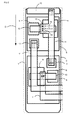
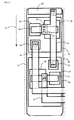
- Figs. 11 to 13 are configuration diagrams of a conventional power semiconductor module.
- Fig. 11 is a plan view showing substantial parts of the conventional power semiconductor module
- Fig. 12 an enlarged view of a section A shown in Fig. 11
- Fig. 13 a schematic cross-sectional view of substantial parts, taken from line X-X of Fig. 11 .
- Fig. 13 also shows a laser beam.
- a power semiconductor module 500 is configured by a heat dissipating base 51, a patterned insulating substrate 56 attached onto the heat dissipating base 51, with a solder 52 therebetween, and a semiconductor chip 58 attached onto a conductive pattern 55 of the patterned insulating substrate 56, with a solder 57 therebetween.
- a conductive film 53 is formed on a rear surface of an insulating substrate 54 and the conductive pattern 55 on a front surface of the same.
- the power semiconductor module 500 is also configured by a lower lead frame 60 attached to an upper surface electrode of the semiconductor chip 58 with a solder 59 therebetween, an upper lead frame 61 laser-welded and attached to the lower lead frame 60, a resin case 62 that is attached to the heat dissipating base 51 by a silicone adhesive 62a and fixed, in a penetrating manner, to the lower lead frame 60 serving as an external terminal, and gel, not shown, which fills the resin case 62.
- the lead frames 60 and 61 are disposed randomly without specifying a direction D of rolling traces 69 (a rolling direction) formed on the lead frames 60 and 61.
- the upper lead frame 61 and the lower lead frame 60 are laser-welded and attached to each other as described above, and the attached portions therebetween are electrically connected to configure current paths.
- a laser beam 64 is radiated from a laser emitting unit 63 onto the upper lead frame 61, to melt and solidify the upper and lower lead frames 60.
- the laser beam 64 is radiated at an angle ⁇ of approximately 10° to 15° with respect to a vertical line 66 on the irradiated surface of the upper lead frame 61. Further, attached portions 65 (laser-welded sections) to be obtained as a result of the radiation of the laser beam 64 are specified by a camera and a light source, not shown, which are installed in the laser emitting unit 63 and a monitor, also not shown, which is installed outside the laser emitting unit 63. Visible light is emitted from the light source. Resultant reflected light from the irradiated surface is complemented by the camera installed in the laser emitting unit 63, and the camera transmits a signal corresponding to the reflected light, to the monitor.
- the irradiation section can be specified. Because the optical axis of this visible light coincides with an optical axis 67 of the laser beam, the visible light, too, is radiated at an angle ⁇ of approximately 10° to 15° with respect to the vertical line 66 on the irradiated surface.
- the number of joining points and joining areas corresponding to the attached portions 65 between the upper lead frame 61 and the lower lead frame 60 are determined in consideration of the conditions under which the power semiconductor module 500 is used (heat generation due to electrification, joint strength in relation to the reliability).
- Extra points between the upper lead frame 61 and the lower lead frame 60 are laser-welded in consideration of inconsistent laser welding occurring therebetween.
- Patent Documents 1 and 2 disclose the technologies for laser-welding a plurality of lead frames.
- Patent Document 3 describes a method of manufacturing a semiconductor device in which a lead frame is roughened for the purpose of reducing the laser welding inconsistency.
- Fig. 14 shows a method of forming a lead frame and Figs. 14(a) to 14(c) are a process diagram showing respective steps in sequence.
- a thick copper plate 72a is rolled with a roll 71 into a copper plate 72 of a predetermined thickness, as shown in Fig. 14(a) .
- a desired lead frame 61 is punched out of the copper plate 72 of the predetermined thickness, as shown in Fig. 14(b) (the upper lead frame is shown in this diagram).
- the lead frame 61 is removed from the copper plate 72, and a predetermined section of the lead frame 61 is bent (not shown), as shown in Fig. 14(c) .
- stripe-shaped rolling traces 69 are formed on the surface of the lead frame 61. Because these rolling traces 69 are formed in the rolling direction D, the direction D of the formed rolling traces 69 is same as the direction D in which the rolling is performed (the rolling direction).
- the direction D of the rolling traces 69 of the upper lead frame 61 lies in a random direction (diagram shows the rolling traces 69 formed in perpendicular and parallel directions) when the upper lead frame 61 is disposed.
- the fact that the direction D of the rolling traces 69 of the upper lead frame 61 lies in a random direction intensifies the fluctuations of the intensity of the visible light reflecting off of the irradiated surface. As a result, the visibility of the camera drops, erroneously detecting the sections to be welded.
- An object of the present invention is to solve the problems described above and to provide a semiconductor device capable of improving the visibility of a camera and reducing false detection of sections to be welded, and a method of manufacturing such semiconductor device.
- an invention according to claim 1 is a semiconductor device including: a heat dissipating base; a patterned insulating substrate attached to the heat dissipating base with a solder therebetween; a semiconductor chip attached to a conductive pattern of the patterned insulating substrate with a solder therebetween; a first conductor attached to the semiconductor chip with a solder therebetween; a resin case attached to the heat dissipating base by an adhesive; and a second conductor attached to the first conductor by laser welding, wherein the second conductor, which is formed by rolling and has stripe-shaped rolling traces formed on a surface thereof in a rolling direction, is disposed on the first conductor such that the rolling traces are arranged in a same direction.
- an optical axis of a laser beam at the time of the laser welding may be tilted with respect to a vertical line vertical to the surface of the second conductor, and the direction of the rolling traces may be made substantially perpendicular to a projection axis obtained by projecting the tilted optical axis onto the surface of the second conductor.
- the first conductor may be a lower lead frame and the second conductor may be an upper lead frame.
- the first conductor may be a heat spreader or the conductive pattern.
- An invention according to claim 5 is a method of manufacturing a semiconductor device, the method including the steps of: radiating visible light to sections to be laser-welded in second conductors; capturing light reflected off of the sections to be laser-welded using a camera; displaying an image from the camera onto a monitor to specify the sections to be laser-welded; and radiating a laser beam onto the specified sections to be laser-welded to laser-weld first conductors and the second conductors together, wherein rolling traces, which are formed by rolling, of all of the second conductors are arranged in a same direction, an emission optical axis of the visible light substantially coincides with an optical axis of the laser beam, the optical axis of the laser beam is tilted with respect to a vertical line vertical to a surface of each of the second conductors, and the direction of the rolling traces is made substantially perpendicular to a projection axis obtained
- the present invention can reduce the fluctuations of the intensity of the light reflected off of each lead frame by arranging the rolling traces of each lead frame in the same direction (the rolling direction), and therefore can improve the visibility of the camera and reduce false detection on the sections to be welded.
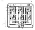
- Figs. 1 to 3 are configuration diagrams of a semiconductor device according to a first example of the present invention.
- Fig. 1 is a plan view showing substantial parts
- Fig. 2 is an enlarged view of a section A shown in Fig. 1
- Fig. 3 is a schematic cross-sectional view of the substantial parts, taken from line X-X of Fig. 1 .
- a semiconductor device 100 shown in Fig. 1 is same as the power semiconductor module 500 shown in Fig. 11 .
- three identical sections including the section A are arranged side by side, and rolling traces 19 (same as the rolling traces 69 of the power semiconductor module 500) of all lead frames are arranged in the direction of the arrow D.
- the direction of the arrow D corresponds to the rolling direction, the direction of the rolling traces 19.
- the semiconductor device 100 is configured by a heat dissipating base 1, a patterned insulating substrate 6 attached to the heat dissipating base 1 with a solder 2 therebetween, and a semiconductor chip 8 attached to a conductive pattern 5 of the patterned insulating substrate 6 with a solder 7 therebetween.
- a conductive film 3 (conductive foil) is formed on the back of an insulating substrate 4 and the conductive pattern 5 on an upper surface of the same.
- the semiconductor device 100 is further configured by a lower lead frame 10 attached to an upper surface electrode of the semiconductor chip 8 with a solder 9 therebetween, an upper lead frame 11 attached by laser welding to the lower lead frame 10, a resin case 12 that is attached to the heat dissipating base 1 by a silicone adhesive 12a and fixed, in a penetrating manner, to the lower lead frame 10 serving as an external terminal, and gel, not shown, which fills the resin case 12.
- the upper lead frame 11 and the lower lead frame 10 are attached to each other by laser-welding, as described above, and attached portions 15 therebetween (laser-welded sections) are electrically connected to configure a current path.
- the attached portions 15 by which the lower lead frame 10 and the upper lead frame 11 are attached to each other are formed by radiating a laser beam 14 from a laser emitting unit 13 to the upper lead frame 11 and melting and solidifying the upper and lower lead frames 10 and 11.
- the laser beam 14 is radiated at an angle ⁇ of approximately 10° to 15° with respect to a vertical line 16 on the irradiated surface of the upper lead frame 11 (the front surface of the upper lead frame 11). Tilting the laser beam 14 in this manner can prevent the upper lead frame 11 from being damaged by reflected light.
- each attached portion 15 where the laser beam 14 is radiated is defined using a camera 25 and an unshown light source which are installed inside the laser emitting unit 13, and a monitor 26 installed outside the laser emitting unit 13.
- visible light emitted light 27
- reflected light 28 from the irradiated surface is complemented by the camera 25 installed inside the laser emitting unit 13.
- a corresponding signal from this camera 25 is transmitted to the monitor 26, and a section to be irradiated is specified by an image displayed on the monitor 26. Because an optical axis 17a of this visible light coincides with an optical axis 17 of the laser beam 14 shown in Fig. 3 , the optical axis 17a of the visible light is tilted as well at approximately 10° to 15° to a vertical line 16a of the irradiated surface.
- Fig. 2 shows the rolling traces 19 formed along the rolling direction D of the upper lead frame 11.
- Fig. 3 (a) shows the rolling traces 19 along with the laser beam 14, and
- Fig. 3(b) shows a projection axis 18 of the laser beam 14 on the upper lead frame 11.
- Fig. 4 is a diagram showing a relationship between each direction of the rolling traces with respect to the projection axis of the visible light and fluctuations in reflection intensity of the visible light.
- the fluctuations become most prominent when the direction D of the rolling traces 19 lies in both perpendicular and parallel directions as in the prior art, and become least prominent when the direction D of the rolling traces 19 lies perpendicularly.
- the upper lead frame 11 is superimposed on the lower lead frame 10, with all of the rolling traces 19 of the upper lead frame 11 arranged in the direction D.
- the diagrams show three types of the upper lead frame 11 and three types of the lower lead frame 10.
- the optical axis 17 of the laser beam 14 is projected onto the upper lead frame 11 in such a manner that the direction D of the rolling traces 19 (same as the rolling direction D) becomes substantially perpendicular to the resultant projection axis 18.
- a projection axis 18a corresponding to the optical axis 17a of the visible light becomes substantially perpendicular to the direction D of the rolling traces 19.
- the term “substantially perpendicular” here covers a range of 90° ⁇ 10°.
- the term “substantially perpendicular” is simply referred to as “perpendicular.”
- the projection axis 18 is an axis obtained by projecting the optical axis 17 of the laser beam 14 onto the upper lead frame immediate therebelow, as shown in Fig. 3 .
- each upper lead frame 11 Because the direction D of the rolling traces 19 of each upper lead frame 11 is made perpendicular to the projection axis 18a of the visible light (the optical axis 17a), the intensity of the light reflected off of the irradiated surface of the attached portions 15 fluctuates less, as shown in Fig. 4 , improving the visibility of the camera 25. Consequently, false detection of the attached portions 15 can be prevented.
- the direction D of the rolling traces 19 (the rolling direction) does not need to be taken into consideration when the directions of the laser emitting unit 13 and the camera 25 or the direction of the semiconductor device 100 (power semiconductor module) can be made variable.
- the configuration of the present invention can eliminate the need for providing a movable mechanism, achieving cost reduction of the device.
- Example 1 has described the example of laser-welding the lead frames 10 and 11 to each other; however, Example 1 can be applied to a case where the upper lead frame 11 is laser-welded to a heat spreader or to the patterned insulating substrate 6.
- Example 1 has also illustrated the case where the projection axis 18a of the visible light (the optical axis 17a) is perpendicular to the direction D of the rolling traces 19; however, the projection axis 18a may be parallel to the direction D of the rolling traces 19.
- arranging the rolling traces 19 in the same direction D can reduce the fluctuations of the intensity of the reflected light of the visible light more than when the direction D of the rolling traces 19 lies in variable directions (in both vertical and parallel directions), as is clear from Fig. 4 .
- the laser beam can be absorbed uniformly in each lead frame, and, thus, inconsistent laser welding results can be lowered.
- the number of points to be welded can be reduced, lowering the manufacturing costs.
- a great effect of the present invention can be expected when the direction of the rolling traces is perpendicular to the projection axis of the laser beam.
- Fig. 5 shows this effect, showing a relationship between each direction of the rolling traces with respect to the projection axis of the laser beam and fluctuations of laser welding.
- the inconsistency is expected to become most prominent when the direction D of the rolling traces 19 lies in both perpendicular and parallel directions as in the prior art, and least prominent when the direction D of the rolling traces 19 lies perpendicularly.
- inconsistent laser welding results are expected to decrease by making the direction D of the rolling traces 19 of the upper lead frame 11 perpendicular to the projection axis 18 of the laser beam 14. As a result, the number of points to be welded can be reduced.
- the alphabet "P” in the diagram represents a high-potential terminal, "N” a low-potential terminal, "U” a U-phase terminal, “V” a V-phase terminal, and "W” a W-phase terminal.
- Figs. 6 to 10 are process diagrams showing a method of manufacturing a semiconductor device according to Example 2 of the present invention, the process diagrams being cross-sectional diagrams showing steps of manufacturing substantial parts of the semiconductor device.
- upper lead frames 11 are cut out of a rolled copper plate 21.
- the places to dispose the upper lead frames 11 in the semiconductor device 100 (power semiconductor module) are predicted, and all of the upper lead frames 11 (the section A is shown) are cut out in such a manner that the rolling traces 19 are arranged in the same direction D (the rolling direction).
- lower lead frames 10 are disposed on a front surface electrode of the semiconductor chips 8.
- the rolling direction of the lower lead frames 10 may or may not have to be the same as that of the upper lead frames 11 and can be any direction.
- the upper lead frames 11 are disposed on the lower lead frames 10 in such a manner that the rolling traces 19 are arranged in the same direction, as shown in Fig. 8 .
- visible light is radiated from the light source of the laser emitting unit 13 onto each upper lead frame 11, and thus obtained reflected light 28 from the irradiated surface is captured by the camera 25, as shown in Fig. 9 .
- a corresponding signal from this camera 25 is transmitted to the monitor 26, specifying an attached portion 15a (laser-welded section) to be laser-welded through an image displayed on the monitor 26.
- the direction D of the rolling traces 19 is perpendicular to the projection axis 18a of the visible light on the upper lead frame 11.
- the laser beam 14 is radiated from the laser emitting unit 13 to the attached portion 15a at an angle ⁇ of approximately 10° to 15° with respect to the vertical line 16 on the surface of the upper lead frame 11, thereby laser-welding the upper lead frames 11 and lower lead frame 10 to each other.
- the direction D of the rolling traces 19 is perpendicular to the projection axis 18 of the laser beam 14 on the upper lead frame 11.
- the visibility of the camera 25 can be improved and, consequently, false detection of the attached portion 15a can be prevented.
- Arranging the direction D of the rolling traces 19 of each upper lead frame 11 in the same direction and making this direction D of the rolling traces 19 perpendicular to the projection axis 18 of the laser beam 14, can not only reduce inconsistent laser welding but also reduce the number of points to be welded.
Landscapes
- Engineering & Computer Science (AREA)
- Physics & Mathematics (AREA)
- Optics & Photonics (AREA)
- Plasma & Fusion (AREA)
- Mechanical Engineering (AREA)
- Laser Beam Processing (AREA)
- Manufacturing & Machinery (AREA)
- Chemical & Material Sciences (AREA)
- Ceramic Engineering (AREA)
- Die Bonding (AREA)
Abstract
Description
- The present invention relates to a semiconductor device such as a power semiconductor module, and a method of manufacturing the semiconductor device.
- With the recent reduction in size and increase in capacity of a power semiconductor module, a power semiconductor chip in a power semiconductor module (e.g., an insulated gate bipolar transistor (IGBT)) is therefore operated at high current density. The crucial problem with such power semiconductor module, therefore, is how to dissipate heat generated therein.
- Specifically, while an upper limit of the guaranteed temperature is set for a joint temperature Tj of a semiconductor chip in a power semiconductor device such as an IGBT, in a one-sided cooling system in which a semiconductor chip is mounted on a heat dissipating base (copper base plate) with a patterned insulating substrate therebetween, heat dissipation from the upper surface of the semiconductor chip is hardly expected because the upper surface of the semiconductor chip is sealed with sealing resin filling the package. As the heat density increases due to the reduction in size and increase in current of the semiconductor chip, the conventional wiring structure in which an aluminum wire is used as a wiring lead to be connected to an upper surface electrode of the chip for bonding cannot easily reduce the joint temperature of the chip to the upper limit guaranteed temperature or lower. Moreover, combined with Joule heating from the aluminum wire, wire fusing may occur, which brings concern that the power cycle resistance of the semiconductor chip becomes low.
- As the means to improve heat dissipation of the upper surface of the semiconductor chip, a lead frame, for example, can be used in place of the aluminum wire. In this case, a lower lead frame is soldered and attached to an upper surface main electrode of the semiconductor chip, and an upper lead frame is disposed on this attached lower lead frame in such a manner as to be superimposed on the ends thereof. A module structure is known in which an upper lead frame and a lower lead frame are laser-welded and attached to each other and used as a heat transfer path to release heat of the semiconductor chip from the upper surface thereof.
-
Figs. 11 to 13 are configuration diagrams of a conventional power semiconductor module.Fig. 11 is a plan view showing substantial parts of the conventional power semiconductor module,Fig. 12 an enlarged view of a section A shown inFig. 11 , andFig. 13 a schematic cross-sectional view of substantial parts, taken from line X-X ofFig. 11 .Fig. 13 also shows a laser beam. - A
power semiconductor module 500 is configured by aheat dissipating base 51, a patternedinsulating substrate 56 attached onto theheat dissipating base 51, with asolder 52 therebetween, and asemiconductor chip 58 attached onto aconductive pattern 55 of the patternedinsulating substrate 56, with asolder 57 therebetween. In the patternedinsulating substrate 56, a conductive film 53 is formed on a rear surface of aninsulating substrate 54 and theconductive pattern 55 on a front surface of the same. - The
power semiconductor module 500 is also configured by alower lead frame 60 attached to an upper surface electrode of thesemiconductor chip 58 with asolder 59 therebetween, anupper lead frame 61 laser-welded and attached to thelower lead frame 60, aresin case 62 that is attached to theheat dissipating base 51 by a silicone adhesive 62a and fixed, in a penetrating manner, to thelower lead frame 60 serving as an external terminal, and gel, not shown, which fills theresin case 62. Thelead frames lead frames - The
upper lead frame 61 and thelower lead frame 60 are laser-welded and attached to each other as described above, and the attached portions therebetween are electrically connected to configure current paths.
When laser-welding thelower lead frame 60 and theupper lead frame 61 to each other, alaser beam 64 is radiated from alaser emitting unit 63 onto theupper lead frame 61, to melt and solidify the upper andlower lead frames 60. - The
laser beam 64 is radiated at an angle θ of approximately 10° to 15° with respect to avertical line 66 on the irradiated surface of theupper lead frame 61.
Further, attached portions 65 (laser-welded sections) to be obtained as a result of the radiation of thelaser beam 64 are specified by a camera and a light source, not shown, which are installed in thelaser emitting unit 63 and a monitor, also not shown, which is installed outside thelaser emitting unit 63. Visible light is emitted from the light source. Resultant reflected light from the irradiated surface is complemented by the camera installed in thelaser emitting unit 63, and the camera transmits a signal corresponding to the reflected light, to the monitor. Through the image displayed on the monitor, the irradiation section can be specified. Because the optical axis of this visible light coincides with anoptical axis 67 of the laser beam, the visible light, too, is radiated at an angle θ of approximately 10° to 15° with respect to thevertical line 66 on the irradiated surface. - The number of joining points and joining areas corresponding to the attached
portions 65 between theupper lead frame 61 and thelower lead frame 60 are determined in consideration of the conditions under which thepower semiconductor module 500 is used (heat generation due to electrification, joint strength in relation to the reliability). - Extra points between the
upper lead frame 61 and thelower lead frame 60 are laser-welded in consideration of inconsistent laser welding occurring therebetween. -
Patent Documents -
Patent Document 3 describes a method of manufacturing a semiconductor device in which a lead frame is roughened for the purpose of reducing the laser welding inconsistency. -
- Patent Document 1: Japanese Patent Application Publication No.
2008-98585 - Patent Document 2: Japanese Patent Application Publication No.
2008-42039 - Patent Document 3: Japanese Patent Application Publication No.
2008-28286 -
Fig. 14 shows a method of forming a lead frame andFigs. 14(a) to 14(c) are a process diagram showing respective steps in sequence. First of all, athick copper plate 72a is rolled with aroll 71 into acopper plate 72 of a predetermined thickness, as shown inFig. 14(a) . Next, a desiredlead frame 61 is punched out of thecopper plate 72 of the predetermined thickness, as shown inFig. 14(b) (the upper lead frame is shown in this diagram). Thereafter, thelead frame 61 is removed from thecopper plate 72, and a predetermined section of thelead frame 61 is bent (not shown), as shown inFig. 14(c) . As a result of rolling thecopper plate 72, stripe-shapedrolling traces 69 are formed on the surface of thelead frame 61. Because theserolling traces 69 are formed in the rolling direction D, the direction D of the formedrolling traces 69 is same as the direction D in which the rolling is performed (the rolling direction). - As shown in
Fig. 13 , the direction D of therolling traces 69 of theupper lead frame 61 lies in a random direction (diagram shows therolling traces 69 formed in perpendicular and parallel directions) when theupper lead frame 61 is disposed. When radiating visible light to theupper lead frame 61 in order to detect the sections to be laser-welded, the fact that the direction D of therolling traces 69 of theupper lead frame 61 lies in a random direction intensifies the fluctuations of the intensity of the visible light reflecting off of the irradiated surface. As a result, the visibility of the camera drops, erroneously detecting the sections to be welded. - A Ni-plated layer having a thickness of approximately 10 µm, for example, is formed on the surface of the lead frame 61 (Cu) in order to increase its absorption rate of the
laser beam 64.
None ofPatent Documents 1 to 3 mentions that the rolling traces of the plurality of lead frames are arranged in the same direction (the rolling direction) to perform laser welding. - An object of the present invention is to solve the problems described above and to provide a semiconductor device capable of improving the visibility of a camera and reducing false detection of sections to be welded, and a method of manufacturing such semiconductor device.
- In order to achieve the object described above, an invention according to
claim 1 is a semiconductor device including: a heat dissipating base; a patterned insulating substrate attached to the heat dissipating base with a solder therebetween; a semiconductor chip attached to a conductive pattern of the patterned insulating substrate with a solder therebetween; a first conductor attached to the semiconductor chip with a solder therebetween; a resin case attached to the heat dissipating base by an adhesive; and a second conductor attached to the first conductor by laser welding, wherein the second conductor, which is formed by rolling and has stripe-shaped rolling traces formed on a surface thereof in a rolling direction, is disposed on the first conductor such that the rolling traces are arranged in a same direction. - In the invention described in
claim 1, according to an invention ofclaim 2, an optical axis of a laser beam at the time of the laser welding may be tilted with respect to a vertical line vertical to the surface of the second conductor, and the direction of the rolling traces may be made substantially perpendicular to a projection axis obtained by projecting the tilted optical axis onto the surface of the second conductor. - In the invention described in
claim 1, according to an invention ofclaim 3, the first conductor may be a lower lead frame and the second conductor may be an upper lead frame. - In the invention described in
claim 1, according to an invention ofclaim 4, the first conductor may be a heat spreader or the conductive pattern.
An invention according toclaim 5 is a method of manufacturing a semiconductor device, the method including the steps of: radiating visible light to sections to be laser-welded in second conductors; capturing light reflected off of the sections to be laser-welded using a camera; displaying an image from the camera onto a monitor to specify the sections to be laser-welded; and radiating a laser beam onto the specified sections to be laser-welded to laser-weld first conductors and the second conductors together, wherein rolling traces, which are formed by rolling, of all of the second conductors are arranged in a same direction, an emission optical axis of the visible light substantially coincides with an optical axis of the laser beam, the optical axis of the laser beam is tilted with respect to a vertical line vertical to a surface of each of the second conductors, and the direction of the rolling traces is made substantially perpendicular to a projection axis obtained by projecting the tilted optical axis onto the surface of each of the second conductors. - The present invention can reduce the fluctuations of the intensity of the light reflected off of each lead frame by arranging the rolling traces of each lead frame in the same direction (the rolling direction), and therefore can improve the visibility of the camera and reduce false detection on the sections to be welded.
- In particular, making the direction of the rolling traces perpendicular to the projection axis of the visible light brings about an effect of reducing the fluctuations of the reflection intensity of the visible light.
The above and other objects, features and advantages of the present invention will become apparent from the following description thereof taken with the accompanying drawings illustrating the embodiment, a preferred example of the present invention. -
-
Fig. 1 is a plan view showing substantial parts of a semiconductor device according to a first example of the present invention; -
Fig. 2 is an enlarged view of a section A shown inFig. 1 ; -
Fig. 3 is a schematic cross-sectional view of the substantial parts, taken from line X-X ofFig. 1 ; -
Fig. 4 is a diagram showing a relationship between each direction of rolling traces with respect to a projection axis of visible light and fluctuations in reflection intensity of the visible light; -
Fig. 5 is a diagram showing a relationship between each direction of the rolling traces with respect to a projection axis of a laser beam and variations of laser welding; -
Fig. 6 is a cross-sectional view showing steps of manufacturing substantial parts of a semiconductor device according to a second example of the present invention; -
Fig. 7 is a cross-sectional view showing steps of manufacturing the substantial parts of the semiconductor device according to the second example of the present invention, the steps following the steps shown inFig. 6 ; -
Fig. 8 is a cross-sectional view showing steps of manufacturing the substantial parts of the semiconductor device according to the second example of the present invention, the steps following the steps shown inFig. 7 ; -
Fig. 9 is a cross-sectional view showing steps of manufacturing the substantial parts of the semiconductor device according to the second example of the present invention, the steps following the steps shown inFig. 8 ; -
Fig. 10 is a cross-sectional view showing steps of manufacturing the substantial parts of the semiconductor device according to the second example of the present invention, the steps following the steps shown inFig. 9 ; -
Fig. 11 is a plan view showing substantial parts of a conventional power semiconductor module; -
Fig. 12 is an enlarged view of a section A shown inFig. 11 ; -
Fig. 13 is a schematic cross-sectional view of substantial parts, taken from line X-X ofFig. 11 ; and -
Fig. 14 shows a method of forming a lead frame andFigs. 14(a) to 14(c) are a process diagram showing respective steps in sequence. - An embodiment of the present invention is described hereinafter based on examples.
-
Figs. 1 to 3 are configuration diagrams of a semiconductor device according to a first example of the present invention.Fig. 1 is a plan view showing substantial parts,Fig. 2 is an enlarged view of a section A shown inFig. 1 , andFig. 3 is a schematic cross-sectional view of the substantial parts, taken from line X-X ofFig. 1 . Asemiconductor device 100 shown inFig. 1 is same as thepower semiconductor module 500 shown inFig. 11 . InFig. 1 , three identical sections including the section A are arranged side by side, and rolling traces 19 (same as the rolling traces 69 of the power semiconductor module 500) of all lead frames are arranged in the direction of the arrow D. The direction of the arrow D corresponds to the rolling direction, the direction of the rolling traces 19. - The
semiconductor device 100 is configured by aheat dissipating base 1, a patterned insulatingsubstrate 6 attached to theheat dissipating base 1 with asolder 2 therebetween, and asemiconductor chip 8 attached to aconductive pattern 5 of the patterned insulatingsubstrate 6 with asolder 7 therebetween. In the patterned insulatingsubstrate 6, a conductive film 3 (conductive foil) is formed on the back of an insulatingsubstrate 4 and theconductive pattern 5 on an upper surface of the same. - The
semiconductor device 100 is further configured by alower lead frame 10 attached to an upper surface electrode of thesemiconductor chip 8 with asolder 9 therebetween, anupper lead frame 11 attached by laser welding to thelower lead frame 10, aresin case 12 that is attached to theheat dissipating base 1 by asilicone adhesive 12a and fixed, in a penetrating manner, to thelower lead frame 10 serving as an external terminal, and gel, not shown, which fills theresin case 12. - The
upper lead frame 11 and thelower lead frame 10 are attached to each other by laser-welding, as described above, and attachedportions 15 therebetween (laser-welded sections) are electrically connected to configure a current path. - The attached
portions 15 by which thelower lead frame 10 and theupper lead frame 11 are attached to each other are formed by radiating alaser beam 14 from alaser emitting unit 13 to theupper lead frame 11 and melting and solidifying the upper and lower lead frames 10 and 11. - The
laser beam 14 is radiated at an angle θ of approximately 10° to 15° with respect to avertical line 16 on the irradiated surface of the upper lead frame 11 (the front surface of the upper lead frame 11). Tilting thelaser beam 14 in this manner can prevent theupper lead frame 11 from being damaged by reflected light. - The position of each attached
portion 15 where thelaser beam 14 is radiated is defined using acamera 25 and an unshown light source which are installed inside thelaser emitting unit 13, and amonitor 26 installed outside thelaser emitting unit 13. As shown inFig. 9 , visible light (emitted light 27) is emitted from the light source, and thus obtained reflected light 28 from the irradiated surface is complemented by thecamera 25 installed inside thelaser emitting unit 13. A corresponding signal from thiscamera 25 is transmitted to themonitor 26, and a section to be irradiated is specified by an image displayed on themonitor 26. Because anoptical axis 17a of this visible light coincides with anoptical axis 17 of thelaser beam 14 shown inFig. 3 , theoptical axis 17a of the visible light is tilted as well at approximately 10° to 15° to avertical line 16a of the irradiated surface. -
Fig. 2 shows the rolling traces 19 formed along the rolling direction D of theupper lead frame 11.Fig. 3 (a) shows the rolling traces 19 along with thelaser beam 14, andFig. 3(b) shows aprojection axis 18 of thelaser beam 14 on theupper lead frame 11. -
Fig. 4 is a diagram showing a relationship between each direction of the rolling traces with respect to the projection axis of the visible light and fluctuations in reflection intensity of the visible light. The fluctuations become most prominent when the direction D of the rolling traces 19 lies in both perpendicular and parallel directions as in the prior art, and become least prominent when the direction D of the rolling traces 19 lies perpendicularly. - In
Figs. 1 to 3 , theupper lead frame 11 is superimposed on thelower lead frame 10, with all of the rolling traces 19 of theupper lead frame 11 arranged in the direction D. The diagrams show three types of theupper lead frame 11 and three types of thelower lead frame 10. As shown inFig. 3 , theoptical axis 17 of thelaser beam 14 is projected onto theupper lead frame 11 in such a manner that the direction D of the rolling traces 19 (same as the rolling direction D) becomes substantially perpendicular to theresultant projection axis 18. In so doing, because theoptical axis 17a of the visible light coincides with theoptical axis 17 of thelaser beam 14, aprojection axis 18a corresponding to theoptical axis 17a of the visible light, too, becomes substantially perpendicular to the direction D of the rolling traces 19. The term "substantially perpendicular" here covers a range of 90° ± 10°. As described below, the term "substantially perpendicular" is simply referred to as "perpendicular." Note that theprojection axis 18 is an axis obtained by projecting theoptical axis 17 of thelaser beam 14 onto the upper lead frame immediate therebelow, as shown inFig. 3 . - Because the direction D of the rolling traces 19 of each
upper lead frame 11 is made perpendicular to theprojection axis 18a of the visible light (theoptical axis 17a), the intensity of the light reflected off of the irradiated surface of the attachedportions 15 fluctuates less, as shown inFig. 4 , improving the visibility of thecamera 25. Consequently, false detection of the attachedportions 15 can be prevented. - The direction D of the rolling traces 19 (the rolling direction) does not need to be taken into consideration when the directions of the
laser emitting unit 13 and thecamera 25 or the direction of the semiconductor device 100 (power semiconductor module) can be made variable. However, the configuration of the present invention can eliminate the need for providing a movable mechanism, achieving cost reduction of the device. - Example 1 has described the example of laser-welding the lead frames 10 and 11 to each other; however, Example 1 can be applied to a case where the
upper lead frame 11 is laser-welded to a heat spreader or to the patterned insulatingsubstrate 6. - Example 1 has also illustrated the case where the
projection axis 18a of the visible light (theoptical axis 17a) is perpendicular to the direction D of the rolling traces 19; however, theprojection axis 18a may be parallel to the direction D of the rolling traces 19. In other words, arranging the rolling traces 19 in the same direction D can reduce the fluctuations of the intensity of the reflected light of the visible light more than when the direction D of the rolling traces 19 lies in variable directions (in both vertical and parallel directions), as is clear fromFig. 4 . - In the conventional power semiconductor module described with reference to
Figs. 11 to 13 , laser-welding a large number of upper lead frames 61 and lower lead frames 60 leads to inconsistent welding results with some unwelded sections and/or sections with welding defects. Therefore, in order to reliably secure points to be welded, the number of points to be laser-welded needs to be more than the actual number of welding points, which increases the manufacturing costs. Inconsistent laser welding includes inconsistent weld depth in the attachedportions 65, protrusion of molten substances resulting from the welding, and fluctuations in the welded areas. - In the configuration of the present example, unlike this prior art, because the visibility of the camera can be improved by arranging the rolling traces of each lead frame in the same direction (the rolling direction), the laser beam can be absorbed uniformly in each lead frame, and, thus, inconsistent laser welding results can be lowered. As a result, the number of points to be welded can be reduced, lowering the manufacturing costs. Particularly, a great effect of the present invention can be expected when the direction of the rolling traces is perpendicular to the projection axis of the laser beam.
-
Fig. 5 shows this effect, showing a relationship between each direction of the rolling traces with respect to the projection axis of the laser beam and fluctuations of laser welding. The inconsistency is expected to become most prominent when the direction D of the rolling traces 19 lies in both perpendicular and parallel directions as in the prior art, and least prominent when the direction D of the rolling traces 19 lies perpendicularly. - As shown in
Fig. 3 , inconsistent laser welding results are expected to decrease by making the direction D of the rolling traces 19 of theupper lead frame 11 perpendicular to theprojection axis 18 of thelaser beam 14. As a result, the number of points to be welded can be reduced. - Further, the alphabet "P" in the diagram represents a high-potential terminal, "N" a low-potential terminal, "U" a U-phase terminal, "V" a V-phase terminal, and "W" a W-phase terminal.
-
Figs. 6 to 10 are process diagrams showing a method of manufacturing a semiconductor device according to Example 2 of the present invention, the process diagrams being cross-sectional diagrams showing steps of manufacturing substantial parts of the semiconductor device.
InFig. 6 , upper lead frames 11 are cut out of a rolledcopper plate 21. In so doing, the places to dispose the upper lead frames 11 in the semiconductor device 100 (power semiconductor module) are predicted, and all of the upper lead frames 11 (the section A is shown) are cut out in such a manner that the rolling traces 19 are arranged in the same direction D (the rolling direction). - Next, lower lead frames 10 are disposed on a front surface electrode of the
semiconductor chips 8. The rolling direction of the lower lead frames 10 may or may not have to be the same as that of the upper lead frames 11 and can be any direction. - Subsequently, the upper lead frames 11 are disposed on the lower lead frames 10 in such a manner that the rolling traces 19 are arranged in the same direction, as shown in
Fig. 8 .
Next, visible light is radiated from the light source of thelaser emitting unit 13 onto eachupper lead frame 11, and thus obtained reflected light 28 from the irradiated surface is captured by thecamera 25, as shown inFig. 9 . A corresponding signal from thiscamera 25 is transmitted to themonitor 26, specifying an attachedportion 15a (laser-welded section) to be laser-welded through an image displayed on themonitor 26. As described above, the direction D of the rolling traces 19 is perpendicular to theprojection axis 18a of the visible light on theupper lead frame 11. - Next, the
laser beam 14 is radiated from thelaser emitting unit 13 to the attachedportion 15a at an angle θ of approximately 10° to 15° with respect to thevertical line 16 on the surface of theupper lead frame 11, thereby laser-welding the upper lead frames 11 andlower lead frame 10 to each other. As described above, the direction D of the rolling traces 19 is perpendicular to theprojection axis 18 of thelaser beam 14 on theupper lead frame 11. - By arranging the rolling traces 19 in the same direction D on each
upper lead frame 11 and making this direction D of the rolling traces 19 perpendicular to theprojection axis 18a of the visible light as described above, the visibility of thecamera 25 can be improved and, consequently, false detection of the attachedportion 15a can be prevented. - Arranging the direction D of the rolling traces 19 of each
upper lead frame 11 in the same direction and making this direction D of the rolling traces 19 perpendicular to theprojection axis 18 of thelaser beam 14, can not only reduce inconsistent laser welding but also reduce the number of points to be welded. - The foregoing description merely illustrates the principle of the present invention. In addition, various modifications and changes can be made by a person skilled in the art. The present invention is not limited to the precise configurations and applications shown and described above. Accordingly, all suitable modifications and equivalents are considered to fall within the scope of the present invention as defined in the appended claims and their equivalents.
-
- 1
- Heat dissipating base
- 2, 7, 9
- Solder
- 3
- Conductive film (conductive foil)
- 4
- Insulating substrate
- 5
- Conductive pattern
- 6
- Patterned insulating substrate
- 8
- Semiconductor chip
- 10
- Lower lead frame
- 11
- Upper lead frame
- 12
- Resin case
- 12a
- Silicone adhesive
- 13
- Laser emitting unit
- 14
- Laser beam
- 15, 15a
- Attached portion
- 16, 16a
- Vertical line
- 17
- Optical axis of laser beam
- 17a
- Optical axis of visible light
- 18
- Projection axis of laser beam
- 18a
- Projection axis of visible light
- 19
- Rolling trace
- 25
- Camera
- 26
- Monitor
- 27
- Emitted light (visible light)
- 28
- Reflected light (visible light)
- D
- Direction of rolling trace (same as rolling direction)
Claims (5)
- A semiconductor device, comprising:a heat dissipating base;a patterned insulating substrate attached to the heat dissipating base with a solder therebetween;a semiconductor chip attached to a conductive pattern of the patterned insulating substrate with a solder therebetween;a first conductor attached to the semiconductor chip with a solder therebetween;a resin case attached to the heat dissipating base by an adhesive; anda second conductor attached to the first conductor by laser welding,wherein the second conductor, which is formed by rolling and has stripe-shaped rolling traces formed on a surface thereof in a rolling direction, is disposed on the first conductor such that the rolling traces are arranged in a same direction.
- The semiconductor device according to claim 1, wherein an optical axis of a laser beam at the time of the laser welding is tilted with respect to a vertical line vertical to the surface of the second conductor, and the direction of the rolling traces is made substantially perpendicular to a projection axis obtained by projecting the tilted optical axis onto the surface of the second conductor.
- The semiconductor device according to claim 1, wherein the first conductor is a lower lead frame and the second conductor is an upper lead frame.
- The semiconductor device according to claim 1, wherein the first conductor is a heat spreader or the conductive pattern.
- A method of manufacturing a semiconductor device, the method comprising the steps of:radiating visible light to sections to be laser-welded in second conductors;capturing light reflected off of the sections to be laser-welded using a camera;displaying an image from the camera onto a monitor to specify the sections to be laser-welded; andradiating a laser beam onto the specified sections to be laser-welded to laser-weld first conductors and the second conductors together,wherein rolling traces, which are formed by rolling, of all of the second conductors are arranged in a same direction, an emission optical axis of the visible light substantially coincides with an optical axis of the laser beam, the optical axis of the laser beam is tilted with respect to a vertical line vertical to a surface of each of the second conductors, and the direction of the rolling traces is made substantially perpendicular to a projection axis obtained by projecting the tilted optical axis onto the surface of each of the second conductors.
Applications Claiming Priority (2)
| Application Number | Priority Date | Filing Date | Title |
|---|---|---|---|
| JP2011002354 | 2011-01-07 | ||
| PCT/JP2011/076141 WO2012093521A1 (en) | 2011-01-07 | 2011-11-14 | Semiconductor device and manufacturing method thereof |
Publications (3)
| Publication Number | Publication Date |
|---|---|
| EP2662893A1 true EP2662893A1 (en) | 2013-11-13 |
| EP2662893A4 EP2662893A4 (en) | 2015-12-02 |
| EP2662893B1 EP2662893B1 (en) | 2020-09-23 |
Family
ID=46457384
Family Applications (1)
| Application Number | Title | Priority Date | Filing Date |
|---|---|---|---|
| EP11854578.9A Active EP2662893B1 (en) | 2011-01-07 | 2011-11-14 | Semiconductor device and manufacturing method thereof |
Country Status (5)
| Country | Link |
|---|---|
| US (1) | US9136209B2 (en) |
| EP (1) | EP2662893B1 (en) |
| JP (1) | JP5633581B2 (en) |
| CN (1) | CN103299420B (en) |
| WO (1) | WO2012093521A1 (en) |
Families Citing this family (3)
| Publication number | Priority date | Publication date | Assignee | Title |
|---|---|---|---|---|
| DE112018007676T5 (en) * | 2018-05-30 | 2021-02-18 | Mitsubishi Electric Corporation | SEMICONDUCTOR MODULE AND POWER CONVERTER |
| DE102018217659B4 (en) * | 2018-10-15 | 2022-08-04 | Vitesco Technologies GmbH | Arrangement and method for producing an electrically conductive connection between two substrates |
| JP2022042621A (en) * | 2020-09-03 | 2022-03-15 | 古河電気工業株式会社 | Method for producing conductive component, and conductive component |
Family Cites Families (21)
| Publication number | Priority date | Publication date | Assignee | Title |
|---|---|---|---|---|
| KR960001607B1 (en) * | 1992-10-21 | 1996-02-02 | Hyundai Electronics Ind | Forming method of semiconductor qfp lead frame and the |
| JPH1166968A (en) * | 1997-08-26 | 1999-03-09 | Daido Steel Co Ltd | Composite lead material and method of manufacturing the same |
| JP3761684B2 (en) * | 1997-09-05 | 2006-03-29 | 株式会社アマダ | Automatic beam machining centering method and apparatus for laser beam machine |
| KR20000057810A (en) * | 1999-01-28 | 2000-09-25 | 가나이 쓰토무 | Semiconductor device |
| JP4352920B2 (en) * | 2004-02-09 | 2009-10-28 | 日産自動車株式会社 | Laser processing head and laser processing method |
| JP2007134584A (en) * | 2005-11-11 | 2007-05-31 | Mitsui High Tec Inc | Method for manufacturing multilayer lead frame and multilayer lead frame manufactured by this method |
| JP4764983B2 (en) * | 2006-07-25 | 2011-09-07 | 富士電機株式会社 | Manufacturing method of semiconductor device |
| JP4984730B2 (en) | 2006-08-09 | 2012-07-25 | 富士電機株式会社 | Semiconductor device |
| JP4765853B2 (en) * | 2006-09-08 | 2011-09-07 | 富士電機株式会社 | Manufacturing method of semiconductor device |
| JP5076440B2 (en) | 2006-10-16 | 2012-11-21 | 富士電機株式会社 | Semiconductor device and manufacturing method of semiconductor device |
| US7944042B2 (en) * | 2007-03-08 | 2011-05-17 | Fuji Electric Device Technology Co., Ltd. | Semiconductor device and method of manufacturing same |
| JP4775327B2 (en) * | 2007-06-06 | 2011-09-21 | 富士電機株式会社 | Manufacturing method of semiconductor device |
| DE112008003425B4 (en) * | 2007-12-20 | 2023-08-31 | Aisin Aw Co., Ltd. | Process for manufacturing a semiconductor device |
| JP5453720B2 (en) * | 2008-02-15 | 2014-03-26 | 富士電機株式会社 | Laser welding method, semiconductor device and manufacturing method thereof |
| US8507320B2 (en) * | 2008-03-18 | 2013-08-13 | Infineon Technologies Ag | Electronic device including a carrier and a semiconductor chip attached to the carrier and manufacturing thereof |
| JP5119139B2 (en) * | 2008-12-12 | 2013-01-16 | 富士電機株式会社 | Semiconductor device and manufacturing method of semiconductor device |
| CN102576706B (en) * | 2010-03-16 | 2015-07-22 | 富士电机株式会社 | Semiconductor device |
| WO2012157584A1 (en) * | 2011-05-13 | 2012-11-22 | 富士電機株式会社 | Semiconductor device and manufacturing method thereof |
| JP5737412B2 (en) * | 2011-09-15 | 2015-06-17 | 富士電機株式会社 | Semiconductor device manufacturing method and semiconductor device manufactured using the manufacturing method |
| JP6001921B2 (en) * | 2012-05-25 | 2016-10-05 | 新光電気工業株式会社 | Wiring board and method of manufacturing wiring board |
| JP5845201B2 (en) * | 2013-03-21 | 2016-01-20 | 株式会社東芝 | Semiconductor device and strain monitoring device |
-
2011
- 2011-11-14 JP JP2012551794A patent/JP5633581B2/en active Active
- 2011-11-14 EP EP11854578.9A patent/EP2662893B1/en active Active
- 2011-11-14 US US13/978,456 patent/US9136209B2/en active Active
- 2011-11-14 CN CN201180064314.2A patent/CN103299420B/en active Active
- 2011-11-14 WO PCT/JP2011/076141 patent/WO2012093521A1/en not_active Ceased
Also Published As
| Publication number | Publication date |
|---|---|
| US9136209B2 (en) | 2015-09-15 |
| WO2012093521A1 (en) | 2012-07-12 |
| CN103299420B (en) | 2016-08-31 |
| JP5633581B2 (en) | 2014-12-03 |
| US20130285221A1 (en) | 2013-10-31 |
| JPWO2012093521A1 (en) | 2014-06-09 |
| EP2662893A4 (en) | 2015-12-02 |
| EP2662893B1 (en) | 2020-09-23 |
| CN103299420A (en) | 2013-09-11 |
Similar Documents
| Publication | Publication Date | Title |
|---|---|---|
| US9399268B2 (en) | Laser welding method, laser welding jig, and semiconductor device | |
| US12080675B2 (en) | Semiconductor device and bonding method | |
| JP4775327B2 (en) | Manufacturing method of semiconductor device | |
| JP6354415B2 (en) | Laser welding machine and laser welding method using the same | |
| US9468993B2 (en) | Method for producing semiconductor device | |
| US8779584B2 (en) | Semiconductor apparatus | |
| US9076782B2 (en) | Semiconductor device and method of manufacturing same | |
| US20100295187A1 (en) | Semiconductor device and method for fabricating the same | |
| US8710644B2 (en) | Semiconductor unit having a power semiconductor and semiconductor apparatus using the same | |
| WO2015136968A1 (en) | Semiconductor device | |
| JP6790372B2 (en) | Semiconductor device | |
| EP2662893B1 (en) | Semiconductor device and manufacturing method thereof | |
| CN113380684B (en) | Manufacturing method, manufacturing device, fixture assembly, semiconductor module and vehicle | |
| JP4798020B2 (en) | Semiconductor device and manufacturing method thereof | |
| JP5119139B2 (en) | Semiconductor device and manufacturing method of semiconductor device | |
| JP7445069B1 (en) | Solar power module and its manufacturing process | |
| CN105874553B (en) | Fuse element, fuse, method of producing fuse, chip fuse and chip circuit | |
| KR101504282B1 (en) | Light emitting device package | |
| US20220384321A1 (en) | Semiconductor module and method for fabricating the same | |
| JP2016162867A (en) | Method for manufacturing side-emitting light emitting device | |
| JP2012142622A (en) | Semiconductor device | |
| JP2004009141A (en) | Method for making a seal weld joint between a stamping screen and a plastic component |
Legal Events
| Date | Code | Title | Description |
|---|---|---|---|
| PUAI | Public reference made under article 153(3) epc to a published international application that has entered the european phase |
Free format text: ORIGINAL CODE: 0009012 |
|
| 17P | Request for examination filed |
Effective date: 20130807 |
|
| AK | Designated contracting states |
Kind code of ref document: A1 Designated state(s): AL AT BE BG CH CY CZ DE DK EE ES FI FR GB GR HR HU IE IS IT LI LT LU LV MC MK MT NL NO PL PT RO RS SE SI SK SM TR |
|
| DAX | Request for extension of the european patent (deleted) | ||
| RIC1 | Information provided on ipc code assigned before grant |
Ipc: H01L 23/373 20060101ALI20151020BHEP Ipc: H01L 23/36 20060101ALI20151020BHEP Ipc: B23K 26/03 20060101ALI20151020BHEP Ipc: B23K 26/20 20140101ALI20151020BHEP Ipc: B23K 26/02 20140101ALI20151020BHEP Ipc: B23K 26/04 20140101ALI20151020BHEP Ipc: H01L 25/00 20060101ALI20151020BHEP Ipc: B23K 26/22 20060101ALI20151020BHEP Ipc: H01L 21/60 20060101ALI20151020BHEP Ipc: H01L 25/07 20060101AFI20151020BHEP Ipc: H01L 23/00 20060101ALI20151020BHEP Ipc: H01L 25/18 20060101ALI20151020BHEP Ipc: H01L 23/48 20060101ALI20151020BHEP |
|
| RA4 | Supplementary search report drawn up and despatched (corrected) |
Effective date: 20151029 |
|
| STAA | Information on the status of an ep patent application or granted ep patent |
Free format text: STATUS: EXAMINATION IS IN PROGRESS |
|
| 17Q | First examination report despatched |
Effective date: 20190709 |
|
| GRAP | Despatch of communication of intention to grant a patent |
Free format text: ORIGINAL CODE: EPIDOSNIGR1 |
|
| STAA | Information on the status of an ep patent application or granted ep patent |
Free format text: STATUS: GRANT OF PATENT IS INTENDED |
|
| INTG | Intention to grant announced |
Effective date: 20200408 |
|
| GRAS | Grant fee paid |
Free format text: ORIGINAL CODE: EPIDOSNIGR3 |
|
| GRAA | (expected) grant |
Free format text: ORIGINAL CODE: 0009210 |
|
| STAA | Information on the status of an ep patent application or granted ep patent |
Free format text: STATUS: THE PATENT HAS BEEN GRANTED |
|
| AK | Designated contracting states |
Kind code of ref document: B1 Designated state(s): AL AT BE BG CH CY CZ DE DK EE ES FI FR GB GR HR HU IE IS IT LI LT LU LV MC MK MT NL NO PL PT RO RS SE SI SK SM TR |
|
| RAP1 | Party data changed (applicant data changed or rights of an application transferred) |
Owner name: FUJI ELECTRIC CO., LTD. |
|
| REG | Reference to a national code |
Ref country code: GB Ref legal event code: FG4D |
|
| RIN1 | Information on inventor provided before grant (corrected) |
Inventor name: MIYASAKA, TOSHIYUKI |
|
| REG | Reference to a national code |
Ref country code: CH Ref legal event code: EP |
|
| REG | Reference to a national code |
Ref country code: IE Ref legal event code: FG4D |
|
| REG | Reference to a national code |
Ref country code: DE Ref legal event code: R096 Ref document number: 602011068730 Country of ref document: DE Ref country code: AT Ref legal event code: REF Ref document number: 1317251 Country of ref document: AT Kind code of ref document: T Effective date: 20201015 |
|
| PG25 | Lapsed in a contracting state [announced via postgrant information from national office to epo] |
Ref country code: HR Free format text: LAPSE BECAUSE OF FAILURE TO SUBMIT A TRANSLATION OF THE DESCRIPTION OR TO PAY THE FEE WITHIN THE PRESCRIBED TIME-LIMIT Effective date: 20200923 Ref country code: SE Free format text: LAPSE BECAUSE OF FAILURE TO SUBMIT A TRANSLATION OF THE DESCRIPTION OR TO PAY THE FEE WITHIN THE PRESCRIBED TIME-LIMIT Effective date: 20200923 Ref country code: BG Free format text: LAPSE BECAUSE OF FAILURE TO SUBMIT A TRANSLATION OF THE DESCRIPTION OR TO PAY THE FEE WITHIN THE PRESCRIBED TIME-LIMIT Effective date: 20201223 Ref country code: FI Free format text: LAPSE BECAUSE OF FAILURE TO SUBMIT A TRANSLATION OF THE DESCRIPTION OR TO PAY THE FEE WITHIN THE PRESCRIBED TIME-LIMIT Effective date: 20200923 Ref country code: NO Free format text: LAPSE BECAUSE OF FAILURE TO SUBMIT A TRANSLATION OF THE DESCRIPTION OR TO PAY THE FEE WITHIN THE PRESCRIBED TIME-LIMIT Effective date: 20201223 Ref country code: GR Free format text: LAPSE BECAUSE OF FAILURE TO SUBMIT A TRANSLATION OF THE DESCRIPTION OR TO PAY THE FEE WITHIN THE PRESCRIBED TIME-LIMIT Effective date: 20201224 |
|
| REG | Reference to a national code |
Ref country code: AT Ref legal event code: MK05 Ref document number: 1317251 Country of ref document: AT Kind code of ref document: T Effective date: 20200923 |
|
| PG25 | Lapsed in a contracting state [announced via postgrant information from national office to epo] |
Ref country code: LV Free format text: LAPSE BECAUSE OF FAILURE TO SUBMIT A TRANSLATION OF THE DESCRIPTION OR TO PAY THE FEE WITHIN THE PRESCRIBED TIME-LIMIT Effective date: 20200923 Ref country code: RS Free format text: LAPSE BECAUSE OF FAILURE TO SUBMIT A TRANSLATION OF THE DESCRIPTION OR TO PAY THE FEE WITHIN THE PRESCRIBED TIME-LIMIT Effective date: 20200923 |
|
| REG | Reference to a national code |
Ref country code: NL Ref legal event code: MP Effective date: 20200923 |
|
| REG | Reference to a national code |
Ref country code: LT Ref legal event code: MG4D |
|
| PG25 | Lapsed in a contracting state [announced via postgrant information from national office to epo] |
Ref country code: CZ Free format text: LAPSE BECAUSE OF FAILURE TO SUBMIT A TRANSLATION OF THE DESCRIPTION OR TO PAY THE FEE WITHIN THE PRESCRIBED TIME-LIMIT Effective date: 20200923 Ref country code: EE Free format text: LAPSE BECAUSE OF FAILURE TO SUBMIT A TRANSLATION OF THE DESCRIPTION OR TO PAY THE FEE WITHIN THE PRESCRIBED TIME-LIMIT Effective date: 20200923 Ref country code: PT Free format text: LAPSE BECAUSE OF FAILURE TO SUBMIT A TRANSLATION OF THE DESCRIPTION OR TO PAY THE FEE WITHIN THE PRESCRIBED TIME-LIMIT Effective date: 20210125 Ref country code: NL Free format text: LAPSE BECAUSE OF FAILURE TO SUBMIT A TRANSLATION OF THE DESCRIPTION OR TO PAY THE FEE WITHIN THE PRESCRIBED TIME-LIMIT Effective date: 20200923 Ref country code: LT Free format text: LAPSE BECAUSE OF FAILURE TO SUBMIT A TRANSLATION OF THE DESCRIPTION OR TO PAY THE FEE WITHIN THE PRESCRIBED TIME-LIMIT Effective date: 20200923 Ref country code: RO Free format text: LAPSE BECAUSE OF FAILURE TO SUBMIT A TRANSLATION OF THE DESCRIPTION OR TO PAY THE FEE WITHIN THE PRESCRIBED TIME-LIMIT Effective date: 20200923 Ref country code: SM Free format text: LAPSE BECAUSE OF FAILURE TO SUBMIT A TRANSLATION OF THE DESCRIPTION OR TO PAY THE FEE WITHIN THE PRESCRIBED TIME-LIMIT Effective date: 20200923 |
|
| PG25 | Lapsed in a contracting state [announced via postgrant information from national office to epo] |
Ref country code: AL Free format text: LAPSE BECAUSE OF FAILURE TO SUBMIT A TRANSLATION OF THE DESCRIPTION OR TO PAY THE FEE WITHIN THE PRESCRIBED TIME-LIMIT Effective date: 20200923 Ref country code: AT Free format text: LAPSE BECAUSE OF FAILURE TO SUBMIT A TRANSLATION OF THE DESCRIPTION OR TO PAY THE FEE WITHIN THE PRESCRIBED TIME-LIMIT Effective date: 20200923 Ref country code: IS Free format text: LAPSE BECAUSE OF FAILURE TO SUBMIT A TRANSLATION OF THE DESCRIPTION OR TO PAY THE FEE WITHIN THE PRESCRIBED TIME-LIMIT Effective date: 20210123 Ref country code: ES Free format text: LAPSE BECAUSE OF FAILURE TO SUBMIT A TRANSLATION OF THE DESCRIPTION OR TO PAY THE FEE WITHIN THE PRESCRIBED TIME-LIMIT Effective date: 20200923 Ref country code: PL Free format text: LAPSE BECAUSE OF FAILURE TO SUBMIT A TRANSLATION OF THE DESCRIPTION OR TO PAY THE FEE WITHIN THE PRESCRIBED TIME-LIMIT Effective date: 20200923 |
|
| REG | Reference to a national code |
Ref country code: DE Ref legal event code: R097 Ref document number: 602011068730 Country of ref document: DE |
|
| PG25 | Lapsed in a contracting state [announced via postgrant information from national office to epo] |
Ref country code: MC Free format text: LAPSE BECAUSE OF FAILURE TO SUBMIT A TRANSLATION OF THE DESCRIPTION OR TO PAY THE FEE WITHIN THE PRESCRIBED TIME-LIMIT Effective date: 20200923 Ref country code: SK Free format text: LAPSE BECAUSE OF FAILURE TO SUBMIT A TRANSLATION OF THE DESCRIPTION OR TO PAY THE FEE WITHIN THE PRESCRIBED TIME-LIMIT Effective date: 20200923 |
|
| REG | Reference to a national code |
Ref country code: CH Ref legal event code: PL |
|
| PG25 | Lapsed in a contracting state [announced via postgrant information from national office to epo] |
Ref country code: LU Free format text: LAPSE BECAUSE OF NON-PAYMENT OF DUE FEES Effective date: 20201114 |
|
| PLBE | No opposition filed within time limit |
Free format text: ORIGINAL CODE: 0009261 |
|
| STAA | Information on the status of an ep patent application or granted ep patent |
Free format text: STATUS: NO OPPOSITION FILED WITHIN TIME LIMIT |
|
| REG | Reference to a national code |
Ref country code: BE Ref legal event code: MM Effective date: 20201130 |
|
| GBPC | Gb: european patent ceased through non-payment of renewal fee |
Effective date: 20201223 |
|
| PG25 | Lapsed in a contracting state [announced via postgrant information from national office to epo] |
Ref country code: LI Free format text: LAPSE BECAUSE OF NON-PAYMENT OF DUE FEES Effective date: 20201130 Ref country code: SI Free format text: LAPSE BECAUSE OF FAILURE TO SUBMIT A TRANSLATION OF THE DESCRIPTION OR TO PAY THE FEE WITHIN THE PRESCRIBED TIME-LIMIT Effective date: 20200923 Ref country code: CH Free format text: LAPSE BECAUSE OF NON-PAYMENT OF DUE FEES Effective date: 20201130 Ref country code: DK Free format text: LAPSE BECAUSE OF FAILURE TO SUBMIT A TRANSLATION OF THE DESCRIPTION OR TO PAY THE FEE WITHIN THE PRESCRIBED TIME-LIMIT Effective date: 20200923 |
|
| 26N | No opposition filed |
Effective date: 20210624 |
|
| PG25 | Lapsed in a contracting state [announced via postgrant information from national office to epo] |
Ref country code: FR Free format text: LAPSE BECAUSE OF NON-PAYMENT OF DUE FEES Effective date: 20201123 Ref country code: IT Free format text: LAPSE BECAUSE OF FAILURE TO SUBMIT A TRANSLATION OF THE DESCRIPTION OR TO PAY THE FEE WITHIN THE PRESCRIBED TIME-LIMIT Effective date: 20200923 Ref country code: IE Free format text: LAPSE BECAUSE OF NON-PAYMENT OF DUE FEES Effective date: 20201114 |
|
| PG25 | Lapsed in a contracting state [announced via postgrant information from national office to epo] |
Ref country code: GB Free format text: LAPSE BECAUSE OF NON-PAYMENT OF DUE FEES Effective date: 20201223 |
|
| PG25 | Lapsed in a contracting state [announced via postgrant information from national office to epo] |
Ref country code: IS Free format text: LAPSE BECAUSE OF FAILURE TO SUBMIT A TRANSLATION OF THE DESCRIPTION OR TO PAY THE FEE WITHIN THE PRESCRIBED TIME-LIMIT Effective date: 20210123 Ref country code: TR Free format text: LAPSE BECAUSE OF FAILURE TO SUBMIT A TRANSLATION OF THE DESCRIPTION OR TO PAY THE FEE WITHIN THE PRESCRIBED TIME-LIMIT Effective date: 20200923 Ref country code: MT Free format text: LAPSE BECAUSE OF FAILURE TO SUBMIT A TRANSLATION OF THE DESCRIPTION OR TO PAY THE FEE WITHIN THE PRESCRIBED TIME-LIMIT Effective date: 20200923 Ref country code: CY Free format text: LAPSE BECAUSE OF FAILURE TO SUBMIT A TRANSLATION OF THE DESCRIPTION OR TO PAY THE FEE WITHIN THE PRESCRIBED TIME-LIMIT Effective date: 20200923 |
|
| PG25 | Lapsed in a contracting state [announced via postgrant information from national office to epo] |
Ref country code: MK Free format text: LAPSE BECAUSE OF FAILURE TO SUBMIT A TRANSLATION OF THE DESCRIPTION OR TO PAY THE FEE WITHIN THE PRESCRIBED TIME-LIMIT Effective date: 20200923 |
|
| PG25 | Lapsed in a contracting state [announced via postgrant information from national office to epo] |
Ref country code: BE Free format text: LAPSE BECAUSE OF NON-PAYMENT OF DUE FEES Effective date: 20201130 |
|
| REG | Reference to a national code |
Ref country code: DE Ref legal event code: R079 Ref document number: 602011068730 Country of ref document: DE Free format text: PREVIOUS MAIN CLASS: H01L0025070000 Ipc: H10D0080200000 |
|
| PGFP | Annual fee paid to national office [announced via postgrant information from national office to epo] |
Ref country code: DE Payment date: 20250930 Year of fee payment: 15 |