EP2660970A1 - Inverter circuit having a junction gate field-effect transistor - Google Patents
Inverter circuit having a junction gate field-effect transistor Download PDFInfo
- Publication number
- EP2660970A1 EP2660970A1 EP13166392.4A EP13166392A EP2660970A1 EP 2660970 A1 EP2660970 A1 EP 2660970A1 EP 13166392 A EP13166392 A EP 13166392A EP 2660970 A1 EP2660970 A1 EP 2660970A1
- Authority
- EP
- European Patent Office
- Prior art keywords
- transistor
- inverter circuit
- transistor device
- gate field
- inverter
- Prior art date
- Legal status (The legal status is an assumption and is not a legal conclusion. Google has not performed a legal analysis and makes no representation as to the accuracy of the status listed.)
- Withdrawn
Links
- 230000005669 field effect Effects 0.000 title claims abstract description 15
- HBMJWWWQQXIZIP-UHFFFAOYSA-N silicon carbide Chemical compound [Si+]#[C-] HBMJWWWQQXIZIP-UHFFFAOYSA-N 0.000 claims abstract description 15
- 229910010271 silicon carbide Inorganic materials 0.000 claims abstract description 15
- 230000007935 neutral effect Effects 0.000 claims description 7
- 238000000034 method Methods 0.000 claims description 4
- 239000004065 semiconductor Substances 0.000 claims description 2
- 238000012986 modification Methods 0.000 description 1
- 230000004048 modification Effects 0.000 description 1
Images
Classifications
-
- H—ELECTRICITY
- H02—GENERATION; CONVERSION OR DISTRIBUTION OF ELECTRIC POWER
- H02M—APPARATUS FOR CONVERSION BETWEEN AC AND AC, BETWEEN AC AND DC, OR BETWEEN DC AND DC, AND FOR USE WITH MAINS OR SIMILAR POWER SUPPLY SYSTEMS; CONVERSION OF DC OR AC INPUT POWER INTO SURGE OUTPUT POWER; CONTROL OR REGULATION THEREOF
- H02M7/00—Conversion of AC power input into DC power output; Conversion of DC power input into AC power output
- H02M7/42—Conversion of DC power input into AC power output without possibility of reversal
- H02M7/44—Conversion of DC power input into AC power output without possibility of reversal by static converters
- H02M7/48—Conversion of DC power input into AC power output without possibility of reversal by static converters using discharge tubes with control electrode or semiconductor devices with control electrode
- H02M7/483—Converters with outputs that each can have more than two voltages levels
- H02M7/487—Neutral point clamped inverters
-
- Y—GENERAL TAGGING OF NEW TECHNOLOGICAL DEVELOPMENTS; GENERAL TAGGING OF CROSS-SECTIONAL TECHNOLOGIES SPANNING OVER SEVERAL SECTIONS OF THE IPC; TECHNICAL SUBJECTS COVERED BY FORMER USPC CROSS-REFERENCE ART COLLECTIONS [XRACs] AND DIGESTS
- Y02—TECHNOLOGIES OR APPLICATIONS FOR MITIGATION OR ADAPTATION AGAINST CLIMATE CHANGE
- Y02B—CLIMATE CHANGE MITIGATION TECHNOLOGIES RELATED TO BUILDINGS, e.g. HOUSING, HOUSE APPLIANCES OR RELATED END-USER APPLICATIONS
- Y02B70/00—Technologies for an efficient end-user side electric power management and consumption
- Y02B70/10—Technologies improving the efficiency by using switched-mode power supplies [SMPS], i.e. efficient power electronics conversion e.g. power factor correction or reduction of losses in power supplies or efficient standby modes
Definitions
- This disclosure relates generally to inverters and, more particularly, to inverters incorporating a normally-on transistor, such as a normally-on junction gate field-effect transistor (JFET).
- a normally-on transistor such as a normally-on junction gate field-effect transistor (JFET).
- JFET normally-on junction gate field-effect transistor
- Inverters are used in a wide variety of applications to change direct current to alternating current. Some inverters provide variable frequency alternating current power to loads, such as alternating current motors on aircraft.
- inverters There are various types of inverters, including two-level inverters, which typically synthesize only two voltage levels, and neutral point clamped inverters, which are able to synthesize three voltage levels. Neutral point clamped inverters produce less distorted voltage waveforms than two-level inverters, as is known.
- Neutral point clamped inverters commonly use normally-off devices for all transistors. These normally-off devices limit a current shoot-through upon loss of gate drive control power but in some instances have higher on-state losses than comparable normally-on devices. Normally-on devices do not limit current shoot-through.
- An example inverter circuit assembly includes at least one first transistor device and at least one second transistor device.
- the second transistor device comprises a normally-on silicon carbide junction gate field-effect transistor.
- the at least one second transistor device is an inner transistor device relative to the at least one first transistor device.
- An example inverter system includes an inverter having at least one inner transistor device and at least one outer transistor device.
- the at least one inner transistor device comprises a normally-on transistor.
- An example method of converting DC power to AC power includes commutating the AC load current through combinations of normally-on and normally-off transistor devices of an inverter circuit.
- an example inverter circuit 10 is a neutral point clamped inverter circuit. Direct current (DC) to alternating current (AC) inverters are commonly used to provide variable frequency and voltage AC power to many loads, particularly AC motors.
- the example inverter circuit 10 is one leg of a three-phase inverter.
- the example inverter circuit 10 forms a portion of an inverter system 22.
- a DC source 20 sends power through the inverter system 22 to an AC motor 24.
- the inverter circuit 10 provides AC power to loads on an aircraft in this example.
- the example inverter circuit 10 includes transistor devices Q1 to Q4.
- the transistor devices Q1 and Q4 are in closer proximity to DC terminals +DC and -DC than the transistor devices Q2 and Q3.
- the transistor devices Q2 and Q3 are in closer proximity to the AC terminal ⁇ than the transistor devices Q1 and Q4.
- the transistor devices Q1 and Q4 are considered outer devices, and the transistor devices Q2 and Q3 are considered inner or middle devices.
- the middle two transistor devices Q2 and Q3 of the example inverter circuit 10 are normally-on and the outer two transistor devices are normally-off. Further, in this example, the middle two transistor devices are depletion mode Silicon Carbide junction gate field-effect transistors (JFETs), and the outer two transistor devices Q1 and Q4 are Silicon Carbide metal-oxide-semiconductor field-effect transistors (MOSFETs). In other examples, the outer transistor devices Q1 and Q4 are other types of MOSFETs, enhancement mode JFETs, or insulated gate bipolar transistors (IGBTs).
- JFETs depletion mode Silicon Carbide junction gate field-effect transistors
- MOSFETs Silicon Carbide metal-oxide-semiconductor field-effect transistors
- the outer transistor devices Q1 and Q4 are other types of MOSFETs, enhancement mode JFETs, or insulated gate bipolar transistors (IGBTs).
- the example inverter circuit 10 also includes diodes D1 to D6.
- the diodes D I to D6 of the example inverter circuit 10 are Silicon Carbide Schottky diodes.
- the example inverter circuit has relatively low conduction losses through Q2 and Q3 due to the low specific on-resistance of Silicon Carbide depletion mode JFETs, which is lower than the specific on-resistance of Silicon Carbide MOSFETs, and Silicon Carbide enhancement mode (normally-off) JFETs.
- the example inverter circuit 10 has an output phase terminal ⁇ that is configured to be clamped to a direct current link center point when gate drive control power is not applied (lost) to all the transistor devices Q1 to Q4. Since normally-off devices are used for Q1 and Q4, there is no inherent shoot-through condition upon loss of gate drive control power to all the transistor devices Q1 to Q4.
- the inverter circuit 10 synthesizes three node voltages ("levels") at the phase output.
- a two-level inverter by contrast, is only able to synthesize two voltage levels. Consequently, the three-level neutral point clamped inverter is able to produce a less distorted waveform than the two-level inverter of the prior art.
- features of the disclosed examples include using silicon carbide normally-on (depletion mode) JFETs for Q2 and Q3, which reduces conduction losses for a given chip area while maintaining insusceptibility to shoot-through faults.
- Another feature of the disclosed examples includes the ability to clamp the output voltage to a DC link center point when no gate drive voltages are applied to all the transistor devices Q1 to Q4. This zero output voltage property may be desirable for powering certain loads.
Landscapes
- Engineering & Computer Science (AREA)
- Power Engineering (AREA)
- Inverter Devices (AREA)
Abstract
Description
- This disclosure relates generally to inverters and, more particularly, to inverters incorporating a normally-on transistor, such as a normally-on junction gate field-effect transistor (JFET).
- Inverters are used in a wide variety of applications to change direct current to alternating current. Some inverters provide variable frequency alternating current power to loads, such as alternating current motors on aircraft.
- There are various types of inverters, including two-level inverters, which typically synthesize only two voltage levels, and neutral point clamped inverters, which are able to synthesize three voltage levels. Neutral point clamped inverters produce less distorted voltage waveforms than two-level inverters, as is known.
- Neutral point clamped inverters commonly use normally-off devices for all transistors. These normally-off devices limit a current shoot-through upon loss of gate drive control power but in some instances have higher on-state losses than comparable normally-on devices. Normally-on devices do not limit current shoot-through.
- An example inverter circuit assembly includes at least one first transistor device and at least one second transistor device. The second transistor device comprises a normally-on silicon carbide junction gate field-effect transistor. The at least one second transistor device is an inner transistor device relative to the at least one first transistor device.
- An example inverter system includes an inverter having at least one inner transistor device and at least one outer transistor device. The at least one inner transistor device comprises a normally-on transistor.
- An example method of converting DC power to AC power includes commutating the AC load current through combinations of normally-on and normally-off transistor devices of an inverter circuit.
- The various features and advantages of the disclosed examples will become apparent to those skilled in the art from the detailed description. The figures that accompany the detailed description can be briefly described as follows:
-
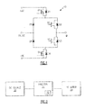
Figure 1 shows an example inverter circuit. -
Figure 2 shows a high level schematic view of a system incorporating the inverter circuit ofFigure 1 . - Referring to
Figures 1 and 2 , anexample inverter circuit 10 is a neutral point clamped inverter circuit. Direct current (DC) to alternating current (AC) inverters are commonly used to provide variable frequency and voltage AC power to many loads, particularly AC motors. Theexample inverter circuit 10 is one leg of a three-phase inverter. - The
example inverter circuit 10 forms a portion of aninverter system 22. ADC source 20 sends power through theinverter system 22 to anAC motor 24. Theinverter circuit 10 provides AC power to loads on an aircraft in this example. - The
example inverter circuit 10 includes transistor devices Q1 to Q4. The transistor devices Q1 and Q4 are in closer proximity to DC terminals +DC and -DC than the transistor devices Q2 and Q3. The transistor devices Q2 and Q3 are in closer proximity to the AC terminal Φ than the transistor devices Q1 and Q4. The transistor devices Q1 and Q4 are considered outer devices, and the transistor devices Q2 and Q3 are considered inner or middle devices. - The middle two transistor devices Q2 and Q3 of the
example inverter circuit 10 are normally-on and the outer two transistor devices are normally-off. Further, in this example, the middle two transistor devices are depletion mode Silicon Carbide junction gate field-effect transistors (JFETs), and the outer two transistor devices Q1 and Q4 are Silicon Carbide metal-oxide-semiconductor field-effect transistors (MOSFETs). In other examples, the outer transistor devices Q1 and Q4 are other types of MOSFETs, enhancement mode JFETs, or insulated gate bipolar transistors (IGBTs). - The
example inverter circuit 10 also includes diodes D1 to D6. The diodes D I to D6 of theexample inverter circuit 10 are Silicon Carbide Schottky diodes. - The example inverter circuit has relatively low conduction losses through Q2 and Q3 due to the low specific on-resistance of Silicon Carbide depletion mode JFETs, which is lower than the specific on-resistance of Silicon Carbide MOSFETs, and Silicon Carbide enhancement mode (normally-off) JFETs.
- The
example inverter circuit 10 has an output phase terminal Φ that is configured to be clamped to a direct current link center point when gate drive control power is not applied (lost) to all the transistor devices Q1 to Q4. Since normally-off devices are used for Q1 and Q4, there is no inherent shoot-through condition upon loss of gate drive control power to all the transistor devices Q1 to Q4. - The
inverter circuit 10 synthesizes three node voltages ("levels") at the phase output. A two-level inverter, by contrast, is only able to synthesize two voltage levels. Consequently, the three-level neutral point clamped inverter is able to produce a less distorted waveform than the two-level inverter of the prior art. - Features of the disclosed examples include using silicon carbide normally-on (depletion mode) JFETs for Q2 and Q3, which reduces conduction losses for a given chip area while maintaining insusceptibility to shoot-through faults. Another feature of the disclosed examples includes the ability to clamp the output voltage to a DC link center point when no gate drive voltages are applied to all the transistor devices Q1 to Q4. This zero output voltage property may be desirable for powering certain loads.
- The preceding description is exemplary rather than limiting in nature. Variations and modifications to the disclosed examples may become apparent to those skilled in the art that do not necessarily depart from the scope of the invention which is defined by the following claims.
Claims (15)
- An inverter circuit assembly, comprising:at least one first transistor device (Q1, Q4); andat least one second transistor device (Q2, Q3) comprising a silicon carbide junction gate field-effect transistor, wherein the at least one second transistor device is an inner transistor device relative to the at least one first transistor device.
- The inverter circuit assembly of claim 1, wherein the inverter circuit comprises two of the first transistor device and two of the second transistor device.
- The inverter circuit assembly of claim 1, wherein the inverter circuit assembly is a neutral point clamped inverter circuit.
- The inverter circuit assembly of claim 1, wherein the silicon carbide junction gate field-effect transistor is a normally-on, depletion mode silicon carbide junction gate field-effect transistor.
- The inverter circuit assembly of claim 1, wherein the at least one first transistor device comprises a Silicon Carbide metal-oxide-semiconductor field-effect transistor, or wherein the at least one first transistor device comprises a junction gate field-effect transistor, or wherein the at least one first transistor device comprises an insulated gate bipolar transistor.
- The inverter circuit assembly of claim 5, wherein the junction gate field-effect transistor is an enhancement mode junction gate field-effect transistor.
- The inverter circuit assembly of claim 1, including an output phase terminal (Φ) configured to be clamped to a direct current link center point when gate drive power is not applied.
- The inverter circuit assembly of claim 1, including diodes (D1-D6), wherein at least some of the diodes are Schottky diodes.
- An inverter system, comprising:an inverter having at least one inner transistor device (Q2, Q3) and at least one outer transistor device (Q1, Q4), wherein the at least one inner transistor device comprises a normally-on transistor.
- The inverter system of claim 9, wherein the inverter circuit comprises no more than two inner transistor devices and at least two outer transistor devices.
- The inverter system of claim 9, wherein a portion of the inverter is a neutral point clamped circuit.
- The inverter system of claim 9, wherein the at least one inner transistor device is a silicon carbide junction gate field-effect transistor.
- A method of converting DC power to AC power comprising:commutating the AC load current through combinations of normally-on and normally-off transistor devices of an inverter circuit.
- The method of claim 13, wherein the normally-on transistor devices are depletion mode silicon carbide junction gate field-effect transistor devices.
- The method of claim 13, including limiting a current shoot-through upon loss of a gate drive control power using the normally-off transistor devices.
Applications Claiming Priority (1)
| Application Number | Priority Date | Filing Date | Title |
|---|---|---|---|
| US13/463,288 US20130294128A1 (en) | 2012-05-03 | 2012-05-03 | Inverter circuit having a junction gate field-effect transistor |
Publications (1)
| Publication Number | Publication Date |
|---|---|
| EP2660970A1 true EP2660970A1 (en) | 2013-11-06 |
Family
ID=48227034
Family Applications (1)
| Application Number | Title | Priority Date | Filing Date |
|---|---|---|---|
| EP13166392.4A Withdrawn EP2660970A1 (en) | 2012-05-03 | 2013-05-03 | Inverter circuit having a junction gate field-effect transistor |
Country Status (2)
| Country | Link |
|---|---|
| US (1) | US20130294128A1 (en) |
| EP (1) | EP2660970A1 (en) |
Cited By (2)
| Publication number | Priority date | Publication date | Assignee | Title |
|---|---|---|---|---|
| CN103701344A (en) * | 2013-12-16 | 2014-04-02 | 上海交通大学无锡研究院 | Three-level inverter and control method thereof |
| EP2937982A3 (en) * | 2014-04-01 | 2017-01-25 | Hamilton Sundstrand Corporation | Switch configuration for a matrix convertor |
Families Citing this family (1)
| Publication number | Priority date | Publication date | Assignee | Title |
|---|---|---|---|---|
| EP4029139A4 (en) | 2019-09-13 | 2023-09-27 | Milwaukee Electric Tool Corporation | Power converters with wide bandgap semiconductors |
Citations (5)
| Publication number | Priority date | Publication date | Assignee | Title |
|---|---|---|---|---|
| FR2943474A1 (en) * | 2009-03-17 | 2010-09-24 | Schneider Toshiba Inverter | Power converter for variable speed drive, has normally open type auxiliary switch positioned in series with each switching arm and connected on negative line of power supply bus, and control device controlling each auxiliary switch |
| JP2010220303A (en) * | 2009-03-13 | 2010-09-30 | Daikin Ind Ltd | Power conversion apparatus |
| DE102009002332A1 (en) * | 2009-04-09 | 2010-10-14 | Infineon Technologies Ag | Multi-level converter i.e. neutral point clamping-type three-level converter, for controlling three-phase motor, has series connections with elements, respectively, where self-conducting and self-locking transistors are provided as elements |
| US7872888B2 (en) * | 2006-03-15 | 2011-01-18 | Kabushiki Kaisha Toshiba | Electric power conversion system |
| US20110199792A1 (en) * | 2008-09-24 | 2011-08-18 | Sma Solar Technology Ag | Converter Comprising at least one Normally on Semiconductor Switch |
Family Cites Families (5)
| Publication number | Priority date | Publication date | Assignee | Title |
|---|---|---|---|---|
| US6838925B1 (en) * | 2003-10-07 | 2005-01-04 | American Power Conversion Corporation | Three level inverter |
| TWI242928B (en) * | 2004-09-10 | 2005-11-01 | Richtek Techohnology Corp | Electronic circuit using normally-on junction field effect transistor |
| JP2007288992A (en) * | 2006-03-20 | 2007-11-01 | Hitachi Ltd | Semiconductor circuit |
| JP2011010404A (en) * | 2009-06-24 | 2011-01-13 | Hitachi Ltd | Power converter, and electric motor drive device and transportation system employing the same |
| EP2302772A1 (en) * | 2009-09-28 | 2011-03-30 | ABB Oy | Inverter |
-
2012
- 2012-05-03 US US13/463,288 patent/US20130294128A1/en not_active Abandoned
-
2013
- 2013-05-03 EP EP13166392.4A patent/EP2660970A1/en not_active Withdrawn
Patent Citations (5)
| Publication number | Priority date | Publication date | Assignee | Title |
|---|---|---|---|---|
| US7872888B2 (en) * | 2006-03-15 | 2011-01-18 | Kabushiki Kaisha Toshiba | Electric power conversion system |
| US20110199792A1 (en) * | 2008-09-24 | 2011-08-18 | Sma Solar Technology Ag | Converter Comprising at least one Normally on Semiconductor Switch |
| JP2010220303A (en) * | 2009-03-13 | 2010-09-30 | Daikin Ind Ltd | Power conversion apparatus |
| FR2943474A1 (en) * | 2009-03-17 | 2010-09-24 | Schneider Toshiba Inverter | Power converter for variable speed drive, has normally open type auxiliary switch positioned in series with each switching arm and connected on negative line of power supply bus, and control device controlling each auxiliary switch |
| DE102009002332A1 (en) * | 2009-04-09 | 2010-10-14 | Infineon Technologies Ag | Multi-level converter i.e. neutral point clamping-type three-level converter, for controlling three-phase motor, has series connections with elements, respectively, where self-conducting and self-locking transistors are provided as elements |
Non-Patent Citations (1)
| Title |
|---|
| SEMIKRON: "Application note AN-11001 - 3L NPC & TNPC Topology", 17 April 2012 (2012-04-17), XP055079875, Retrieved from the Internet <URL:http://www.semikron.com/skcompub/ko/AN11001-rev03_3L_NPC_TNPC_Topology.pdf> [retrieved on 20130918] * |
Cited By (2)
| Publication number | Priority date | Publication date | Assignee | Title |
|---|---|---|---|---|
| CN103701344A (en) * | 2013-12-16 | 2014-04-02 | 上海交通大学无锡研究院 | Three-level inverter and control method thereof |
| EP2937982A3 (en) * | 2014-04-01 | 2017-01-25 | Hamilton Sundstrand Corporation | Switch configuration for a matrix convertor |
Also Published As
| Publication number | Publication date |
|---|---|
| US20130294128A1 (en) | 2013-11-07 |
Similar Documents
| Publication | Publication Date | Title |
|---|---|---|
| CN102449898B (en) | Power conversion device | |
| US10707776B2 (en) | 3-level power conversion circuit including serially-connected switching element and diode | |
| US9979322B2 (en) | Modulator for a hybrid converter system | |
| EP2381567A1 (en) | Bidirectional switch circuit and power converter provided with same | |
| US9143078B2 (en) | Power inverter including SiC JFETs | |
| US20170237359A1 (en) | Inverter | |
| JP6136011B2 (en) | Semiconductor device and power conversion device | |
| US10090778B2 (en) | Multi-phase power device with two-phase modulation scheme | |
| EP3484038B1 (en) | Method and system for operating a phase-leg of a three-level active neutral point clamped converter | |
| JP2010220303A (en) | Power conversion apparatus | |
| US20220337176A1 (en) | Inverter circuit control method and related apparatus | |
| EP2937982A2 (en) | Switch configuration for a matrix convertor | |
| US10050553B2 (en) | Rectifier circuit including a self-clamping transistor | |
| US20160365806A1 (en) | Regenerative converter | |
| CN104518700A (en) | Driver circuit for a pair of semiconductor switches in a leg of a three-level inverter half-bridge | |
| US10312227B2 (en) | Power semiconductor module | |
| EP3273588A1 (en) | Inverter circuit and power conversion device | |
| US9960702B2 (en) | Switch device, power conversion device, motor drive device, air blower, compressor, air conditioner, refrigerator, and freezer | |
| JP2019024289A (en) | Driving method of power converter | |
| WO2000072433A1 (en) | Switching circuit | |
| US20130294128A1 (en) | Inverter circuit having a junction gate field-effect transistor | |
| US10770985B2 (en) | Vehicle auxiliary power supply device | |
| EP2884649A1 (en) | Inverter drive circuit | |
| EP2648329A1 (en) | Three-phase inverter for driving an electric motor having cascode power switches | |
| US9564833B2 (en) | Solid-state inverters with voltage-balanced switches |
Legal Events
| Date | Code | Title | Description |
|---|---|---|---|
| PUAI | Public reference made under article 153(3) epc to a published international application that has entered the european phase |
Free format text: ORIGINAL CODE: 0009012 |
|
| AK | Designated contracting states |
Kind code of ref document: A1 Designated state(s): AL AT BE BG CH CY CZ DE DK EE ES FI FR GB GR HR HU IE IS IT LI LT LU LV MC MK MT NL NO PL PT RO RS SE SI SK SM TR |
|
| AX | Request for extension of the european patent |
Extension state: BA ME |
|
| 17P | Request for examination filed |
Effective date: 20140430 |
|
| RBV | Designated contracting states (corrected) |
Designated state(s): AL AT BE BG CH CY CZ DE DK EE ES FI FR GB GR HR HU IE IS IT LI LT LU LV MC MK MT NL NO PL PT RO RS SE SI SK SM TR |
|
| 17Q | First examination report despatched |
Effective date: 20170619 |
|
| STAA | Information on the status of an ep patent application or granted ep patent |
Free format text: STATUS: THE APPLICATION IS DEEMED TO BE WITHDRAWN |
|
| 18D | Application deemed to be withdrawn |
Effective date: 20171031 |