EP2660821A1 - Sampling device with time-interleaved optical clocking - Google Patents
Sampling device with time-interleaved optical clocking Download PDFInfo
- Publication number
- EP2660821A1 EP2660821A1 EP12167613.4A EP12167613A EP2660821A1 EP 2660821 A1 EP2660821 A1 EP 2660821A1 EP 12167613 A EP12167613 A EP 12167613A EP 2660821 A1 EP2660821 A1 EP 2660821A1
- Authority
- EP
- European Patent Office
- Prior art keywords
- track
- optical
- sampling device
- branch
- hold
- Prior art date
- Legal status (The legal status is an assumption and is not a legal conclusion. Google has not performed a legal analysis and makes no representation as to the accuracy of the status listed.)
- Granted
Links
Images



Classifications
-
- G—PHYSICS
- G11—INFORMATION STORAGE
- G11C—STATIC STORES
- G11C27/00—Electric analogue stores, e.g. for storing instantaneous values
- G11C27/02—Sample-and-hold arrangements
-
- G—PHYSICS
- G02—OPTICS
- G02B—OPTICAL ELEMENTS, SYSTEMS OR APPARATUS
- G02B6/00—Light guides; Structural details of arrangements comprising light guides and other optical elements, e.g. couplings
- G02B6/10—Light guides; Structural details of arrangements comprising light guides and other optical elements, e.g. couplings of the optical waveguide type
- G02B6/12—Light guides; Structural details of arrangements comprising light guides and other optical elements, e.g. couplings of the optical waveguide type of the integrated circuit kind
- G02B6/122—Basic optical elements, e.g. light-guiding paths
- G02B6/125—Bends, branchings or intersections
-
- G—PHYSICS
- G02—OPTICS
- G02F—OPTICAL DEVICES OR ARRANGEMENTS FOR THE CONTROL OF LIGHT BY MODIFICATION OF THE OPTICAL PROPERTIES OF THE MEDIA OF THE ELEMENTS INVOLVED THEREIN; NON-LINEAR OPTICS; FREQUENCY-CHANGING OF LIGHT; OPTICAL LOGIC ELEMENTS; OPTICAL ANALOGUE/DIGITAL CONVERTERS
- G02F7/00—Optical analogue/digital converters
-
- G—PHYSICS
- G11—INFORMATION STORAGE
- G11C—STATIC STORES
- G11C27/00—Electric analogue stores, e.g. for storing instantaneous values
- G11C27/02—Sample-and-hold arrangements
- G11C27/024—Sample-and-hold arrangements using a capacitive memory element
-
- H—ELECTRICITY
- H03—ELECTRONIC CIRCUITRY
- H03K—PULSE TECHNIQUE
- H03K3/00—Circuits for generating electric pulses; Monostable, bistable or multistable circuits
- H03K3/02—Generators characterised by the type of circuit or by the means used for producing pulses
- H03K3/42—Generators characterised by the type of circuit or by the means used for producing pulses by the use, as active elements, of opto-electronic devices, i.e. light-emitting and photoelectric devices electrically- or optically-coupled
-
- H—ELECTRICITY
- H03—ELECTRONIC CIRCUITRY
- H03M—CODING; DECODING; CODE CONVERSION IN GENERAL
- H03M1/00—Analogue/digital conversion; Digital/analogue conversion
- H03M1/12—Analogue/digital converters
- H03M1/124—Sampling or signal conditioning arrangements specially adapted for A/D converters
- H03M1/1245—Details of sampling arrangements or methods
-
- G—PHYSICS
- G02—OPTICS
- G02B—OPTICAL ELEMENTS, SYSTEMS OR APPARATUS
- G02B6/00—Light guides; Structural details of arrangements comprising light guides and other optical elements, e.g. couplings
- G02B6/10—Light guides; Structural details of arrangements comprising light guides and other optical elements, e.g. couplings of the optical waveguide type
- G02B6/12—Light guides; Structural details of arrangements comprising light guides and other optical elements, e.g. couplings of the optical waveguide type of the integrated circuit kind
- G02B2006/12133—Functions
- G02B2006/12147—Coupler
-
- G—PHYSICS
- G02—OPTICS
- G02B—OPTICAL ELEMENTS, SYSTEMS OR APPARATUS
- G02B6/00—Light guides; Structural details of arrangements comprising light guides and other optical elements, e.g. couplings
- G02B6/10—Light guides; Structural details of arrangements comprising light guides and other optical elements, e.g. couplings of the optical waveguide type
- G02B6/12—Light guides; Structural details of arrangements comprising light guides and other optical elements, e.g. couplings of the optical waveguide type of the integrated circuit kind
- G02B2006/12133—Functions
- G02B2006/1215—Splitter
-
- G—PHYSICS
- G02—OPTICS
- G02B—OPTICAL ELEMENTS, SYSTEMS OR APPARATUS
- G02B6/00—Light guides; Structural details of arrangements comprising light guides and other optical elements, e.g. couplings
- G02B6/10—Light guides; Structural details of arrangements comprising light guides and other optical elements, e.g. couplings of the optical waveguide type
- G02B6/12—Light guides; Structural details of arrangements comprising light guides and other optical elements, e.g. couplings of the optical waveguide type of the integrated circuit kind
- G02B2006/12133—Functions
- G02B2006/12154—Power divider
-
- G—PHYSICS
- G02—OPTICS
- G02B—OPTICAL ELEMENTS, SYSTEMS OR APPARATUS
- G02B6/00—Light guides; Structural details of arrangements comprising light guides and other optical elements, e.g. couplings
- G02B6/24—Coupling light guides
- G02B6/26—Optical coupling means
- G02B6/28—Optical coupling means having data bus means, i.e. plural waveguides interconnected and providing an inherently bidirectional system by mixing and splitting signals
- G02B6/2804—Optical coupling means having data bus means, i.e. plural waveguides interconnected and providing an inherently bidirectional system by mixing and splitting signals forming multipart couplers without wavelength selective elements, e.g. "T" couplers, star couplers
- G02B6/2861—Optical coupling means having data bus means, i.e. plural waveguides interconnected and providing an inherently bidirectional system by mixing and splitting signals forming multipart couplers without wavelength selective elements, e.g. "T" couplers, star couplers using fibre optic delay lines and optical elements associated with them, e.g. for use in signal processing, e.g. filtering
-
- G—PHYSICS
- G11—INFORMATION STORAGE
- G11C—STATIC STORES
- G11C13/00—Digital stores characterised by the use of storage elements not covered by groups G11C11/00, G11C23/00, or G11C25/00
- G11C13/04—Digital stores characterised by the use of storage elements not covered by groups G11C11/00, G11C23/00, or G11C25/00 using optical elements ; using other beam accessed elements, e.g. electron or ion beam
-
- H—ELECTRICITY
- H03—ELECTRONIC CIRCUITRY
- H03M—CODING; DECODING; CODE CONVERSION IN GENERAL
- H03M1/00—Analogue/digital conversion; Digital/analogue conversion
- H03M1/12—Analogue/digital converters
- H03M1/1205—Multiplexed conversion systems
- H03M1/121—Interleaved, i.e. using multiple converters or converter parts for one channel
- H03M1/1215—Interleaved, i.e. using multiple converters or converter parts for one channel using time-division multiplexing
Definitions
- the invention relates to a sampling device which comprises a plurality of track-and-hold-units that are operated in a time-interleaved mode.
- the increasing need for wideband communication systems drives an increasing demand for suitable measurement systems.
- the measurement systems need a really high bandwidth and a good jitter performance.
- the whole clock tree has to be stabilized.
- the inventive sampling device comprises a first input port and a second input port, wherein an input-signal is fed to the first input port and wherein an optical clock signal is fed to the second input port.
- the sampling device further comprises a plurality of track-and-hold-units, wherein each of the plurality of the track-and-hold-units is connected to the first input port and wherein the plurality of the track-and-hold-units is also connected to the second input port through an optical waveguide in such a manner that the plurality of the track-and-hold-units operate in a time-interleaved mode.
- a plurality of track-and-hold-units are used and that a single optical clock signal can be forwarded to those plurality of track-and-hold-units, so that only one light source is needed. It is further beneficial that the plurality of the track-and-hold-units operate in a time-interleaved mode. This ensures that the input-signal is captured by the plurality of the track-and-hold-units at different times, thereby allowing each of the plurality of the track-and-hold-units to store a part of the input-signal for a longer time.
- each delay unit is a part of the optical waveguide and if each delay unit has the shape of a meander and/or if each delay unit has segments that are parallel to each other and if each delay unit has other segments that connect the parallel segments to each other, wherein the other segments are round having a diameter that is equal or larger than the distance between the two parallel segments.
- the use of such delay units, that have the shape of a meander having parallel segments as well as the use of the other round segments connecting the parallel segments to each other ensure that the power loss of the optical clock signal is minimized.
- no corners or other disadvantageous changeovers are used within the delay units.
- the delay unit is a part of the optical waveguide and if this part of the optical waveguide, which forms the delay unit, has the shape of a spiral, wherein an inner segment of the delay unit which is also an inner segment of the spiral is lead to the outside within a straight line, thereby crossing the other segments at an angle of about 90°. If an angle of 90° is maintained, it is possible that the optical clock signal in different segments of the optical waveguide can cross itself without interfering itself. Therefore, the optical waveguide can be applied very easily.
- the optical waveguide comprises N-1 optical power dividers, wherein N is the number of the plurality of the track-and-hold-units, wherein each optical power divider splits the optical waveguide into a first branch and a second branch, and/or if the ratio of the signal power at each branch can be selected by adjusting the divergency angle of the first branch and the divergency angle of the second branch with respect to an incoming signal line of the optical power divider.
- the use of such optical power dividers is very helpful, because the jitter performance is not degraded. It is also very useful, if the signal power at each branch can be adjusted, because it can be guaranteed that each of the plurality of the track-and-hold-units receives the same signal level.
- the N-1 optical power dividers are connected in the structure of a binary tree whose root is located at the second input port and whose N terminal branches connect to the N track-and-hold units.
- the terminal branches are also the leaf nodes of the binary tree. It should be noted, that all kinds of binary trees can be used, like a perfect binary tree or a complete binary tree.
- At least one delay unit is arranged within the second branch of each of the N-1 optical power dividers. This ensures that every track-and-hold-unit operates at a different time, so that every track-and-hold-unit captures a different part of the input-signal.
- the depths of all branches of the tree-structure comprising all descendants of the first optical power divider are the same and/or if the number of the delay units that are ranged within the second branch of every optical power divider equals the number of the track-and-hold-units that are connected as descendants to that respective branch and/or if no delay unit is arranged within the first branch of every optical power divider.
- the sampling device comprises a plurality of opto-electronic flip-flops, wherein each of the plurality of the opto-electronic flip-flops transforms the optical clock signal into an electrical clock signal, wherein each of the plurality of the opto-electronic flip-flops connects each of the track-and-hold-units to the optical waveguide.
- the optical waveguide is made of a layer of germanium or SiO 2 and/or if the optical waveguide, the optical power splitters and the delay units are made of germanium or SiO 2 and if they are arranged on a first part of the wafer and if the plurality of the track-and-hold-units and the opto-electronic flip-flops are made of SiGe and if they are arranged on a second part of the wafer and if the opto-electric flip-flop comprises a photodiode that is arranged in between the two parts of the wafer.
- a mode locked laser is used to generate the optical clock signal and if the mode locked laser is connected through an optical fiber to the second input port.
- a mode locked laser has very good jitter performance as well as an output power on the order of 30 mW.
- Fig. 1 shows a high-speed sampling unit 1 comprising the sampling device 2, which in turn comprises track-and-hold-units 7 1 , 7 2 to 7 N which are operated in a time-interleaved mode.
- the high-speed sampling unit 1 can be integrated within a single chip or ASIC.
- the sampling device 2 can be integrated on a chip of its own while the analog/digital-converters 3 1 , 3 2 to 3 N are located on separate chips. It should be noted, that the analog/digital-converters 3 1 , 3 2 to 3 N are only incorporated within Fig. 1 for a better understanding and that they are not a necessary part of the invention.
- the sampling device 2 further comprises a first input port 4 and a second input port 5.
- An electrical input-signal i.e. a RF-signal
- the RF-signal is a high-frequency signal having a bandwidth of approximately up to 30 GHz and above.
- the RF-signal is then amplified by at least one amplifier 6. However, if N is small, for example four or eight the RF-signal does not need to be amplified.
- the amplification factor of the at least one amplifier 6 is preferably adjustable.
- the amplified RF-signal is then fed to each of a plurality of the track-and-hold-units 7 1 , 7 2 to 7 N .
- the amplified RF-signal can therefore be split up for example by using a 3-dB hybrid-coupler. It is also possible to abstain from using a 3-dB hybrid-coupler within a chip, because the signal lines should be short enough.
- the high-speed sampling unit 1 comprises an optical clock source 8.
- the optical clock source is preferably a mode locked laser 8.
- the mode locked laser 8 is difficult to integrate within a chip together with the other components of the high-speed sampling unit 1.
- the mode locked laser 8 generates an optical clock signal having a frequency f clk of, for example, 10 GHz.
- the energy for each pulse exceeds for example 3 pJ and the timing jitter is smaller than 20 fs RMS.
- the sampling device 2 preferably comprises the at least one amplifier 6, the plurality of the track-and-hold-units 7 1 , 7 2 to 7 N as well as at least one optical power divider 9 and at least one delay unit 10 1 , 10 2 .
- the mode locked laser 8 is connected to the second input port by using an optical fiber.
- an optical waveguide 11 is used to lead the optical clock signal to each of the plurality of the track-and-hold-units 7 1 , 7 2 to 7 N . It is very important that the optical clock signal is fed to the plurality of the track-and-hold-units 7 1 , 7 2 to 7 N in such a manner that the plurality of the track-and-hold-units are operated in a time-interleaved mode.
- the second input port 5 which is connected to the optical waveguide 11 is connected to a first optical power divider 9.
- a first branch of the first optical power divider is connected to the first track-and-hold-unit 7 1 .
- a second branch of the first optical power divider 9 is connected to a first delay unit 10 1 .
- the first delay unit 10 1 is further connected to a another delay unit 10 M , wherein M ⁇ 1 and M ⁇ .
- Within the first delay unit 10 1 there is also another optical power divider which splits up the optical clock signal into a signal that is fed to the second track-and-hold-unit 7 2 . Another signal of the another optical power divider is then fed to the other track-and-hold-units 7 N , wherein N ⁇ 2 and N ⁇ .
- Each of the plurality of the track-and-hold-units 7 1 , 7 2 to 7 N comprises further a plurality of opto-electronic flip-flops 12 1 , 12 2 to 12 N which transform the optical clock signal into an electrical clock signal.
- the plurality of the opto-electronic flip-flops 12 1 , 12 2 to 12 N therefore connect each of the track-and-hold-units 7 1 , 7 2 to 7 N to the optical waveguide 11.
- the plurality of the opto-electronic flip-flops 12 1 , 12 2 to 12 N also enhance the duty cycle of the electrical clock signal to approximately 50%.
- the opto-electronic flip-flops 12 1 , 12 2 to 12 N can be integrated within the track-and-hold-units 7 1 , 7 2 to 7 N , but they can also be separated from the respective track-and-hold-units 7 1 , 7 2 to 7 N . Thus they can be integrated somewhere in the sampling device 2.
- each of the plurality of the track-and-hold-units 7 1 , 7 2 to 7 N is preferably connected to an amplifier 13 1 , 13 2 to 13 N .
- the amplifiers 13 1 , 13 2 to 13 N drive the inputs of the analog/digital converters.
- the analog/digital-converters 3 1 , 3 2 to 3 N are preferably arranged outside of the chip, because the chip may not be large enough.
- Each of the analog/digital-converters 3 1 , 3 2 to 3 N has a plurality of parallel output ports which can be used for a high-speed data transfer.
- Fig. 2 shows a sampling device 2 according to the present invention.
- the sampling device 2 comprises a plurality of track-and-hold-units 7 1 , 7 2 to 7 N .
- the interleaving factor N equals eight, which also means that there are eight track-and-hold-units 7 1 , 7 2 to 7 N .
- Each delay unit 10 1 , 10 M is a part of the optical waveguide 11 which is explained in detail below.
- the optical waveguide 11 further comprises N-1 optical power dividers 9 1 to 9 N-1 wherein N is the interleaving factor as well as the number of the plurality of the track-and-hold-units 7 1 , 7 2 to 7 N .
- Each optical power divider 9 1 to 9 N-1 splits the optical waveguide 11 into a first branch and into a second branch. If the optical waveguide 11 is nearly lossless, each branch should get half the incoming optical power. In practice, the optical waveguide may have substantial losses, whereby a larger attenuation will occur on a branch with a large delay compared to a branch with a small delay. In this case, it is preferable to provide more power to the branch with a large delay so that the power at the output of each branch will be substantially equal.
- the ratio of the signal power at each branch can be selected by adjusting the divergency angle of the first branch and the divergency angle of the second branch with respect to the incoming signal line of the respective optical power divider 9 1 to 9 N-1 . These details will also be explained below.
- the ratio of the signal power of all N-1 optical power dividers 9 1 to 9 N-1 is adjusted in such a way that the signal power at each end node of the optical waveguide 11 or at each of the plurality of the track-and-hold-units 7 1 , 7 2 to 7 N is approximately the same.
- the ratio of the signal power of all N-1 optical power dividers 9 1 to 9 N-1 has to be adjusted in such a way that the signal power should be the same at the input port of the plurality of the opto-electronic flip-flops 12 1 , 12 2 to 12 N , wherein the opto-electronic flip-flops 12 1 , 12 2 to 12 N are integrated within the track-and-hold-units 7 1 , 7 2 to 7 N or wherein the opto-electronic flip-flops 12 1 to 12 N are arranged in front of the track-and-hold-units 7 1 , 7 2 to 7 N , i.e. upstream in the signal path.
- Fig. 2 describes a symmetrical tree-structure of the optical waveguide 11. This means that the depth of all branches of the tree-structure is the same, wherein the tree-structure comprises all descendants of the first optical power divider 9 1 .
- the descendants comprise the further optical power dividers 9 2 to 9 N-1 as well as the plurality of the delay units 10 1 , 10 2 to 10 M .
- the descendants are connected to the first branch or the second branch of the first optical power divider 9 1 .
- the first optical power divider 9 1 is thereby connected to the second input port 5.
- the depth of the tree-structure is three.
- the number of the delay units 10 1 to 10 M arranged within a second branch of every optical power divider 9 1 to 9 N-1 equals the number of the track-and-hold-units 7 1 , 7 2 to 7 N that are connected as descendants to the respective branch.
- the second branch of the first optical divider 9 1 comprises four delay units 10 1 . This is indicated by the number "4" before ⁇ t.
- the second branch of the first optical divider 9 1 is connected to four track-and-hold-units 7 1 , 7 2 to 7 N at the end.
- the same also applies to the second branch of the second optical divider 9 2 .
- the second branch of the second optical divider 9 2 is connected to two track-and-hold-units 7 1 , 7 2 to 7 N , which means that two delay units 10 2 are incorporated within the second branch of the second optical power divider 9 2 .
- a branch is a line segment of the optical waveguide 11 that extends from the output of each of the optical power dividers 9 1 to 9 N-1 and ends at the input of the descendant optical power divider 9 1 to 9 N-1 or at the input port of the opto-electronic flip-flop 12 1 to 12 N or at the input port of the track-and-hold-unit 7 1 , 7 2 to 7 N .
- a delay unit 10 1 to 10 M can be incorporated into each branch .
- the delay unit 10 1 to 10 M is an integral part of the optical waveguide 11 having a special wiring.
- the optical clock signal for the second track-and-hold-unit 7 2 is delayed by 12.5 ps. It is also clear that the clock signal for the third track-and-hold-unit 7 3 is delayed by 25 ps compared to the clock signal fed to the first track-and-hold-unit 7 1 .
- the amount of the descendant branches have to be taken into account comprising the amount of the descendant delay units 9 1 to 9 N-1 .
- the first branch of the first optical power divider 9 1 comprises four descendant delay units 10 1 to 10 M
- the second branch of the first optical power divider 9 1 comprises eight delay units 10 1 to 10 M .
- the at least one delay unit 10 1 to 10 M delays the optical clock signal in such a manner that each of the plurality of the track-and-hold-units 7 1 , 7 2 to 7 N captures a part of the RF (radio frequency)-input-signal at a different time.
- the N-1 optical power dividers 9 1 to 9 N-1 can be connected in series so that each optical power divider 9 1 to 9 N is connected to the second branch of a respective parent optical power divider 9 1 to 9 N-1 , wherein the first optical power divider 9 1 is connected to the second input port 5 and wherein the first branch of each of the N-1 optical power dividers 9 1 to 9 N-1 is connected to the respective track-and-hold-unit 7 1 , 7 2 to 7 N .
- Fig. 1 Such a structure is shown in Fig. 1 for example.
- one delay unit 10 1 to 10 M is arranged within the second branch of each of the N-1 optical power dividers 9 1 to 9 N-1 .
- This kind of tree-structure can preferably be used if the number of the track-and-hold-units 7 1 , 7 2 to 7 N is small.
- the division ratio within the first optical power divider 9 1 can easily be adjusted.
- the first optical power divider 9 1 should have a division ratio of at least 1:32 which is difficult to obtain.
- the plurality of the track-and-hold-units 7 1 , 7 2 to 7 N are connected to the plurality of amplifiers 13 1 to 13 N , wherein the output of the plurality of the amplifiers 13 1 to 13 N is preferably also the output of the chip.
- Fig. 3 shows a simplified layout of the sampling device 2 according to an embodiment of the present invention.
- an RF-signal is fed to the first input port 4.
- the RF-signal is split into N individual signals which are fed to the plurality of the track-and-hold-units 7 1 , 7 2 to 7 N .
- the RF-distribution circuit 30 comprises several amplifiers 6 for amplifying each of the individual RF-signals. It should be noted that the RF-distribution circuit 30 is matched with respect to the first input port 4.
- an optical clock signal is fed to the second input port 5.
- This optical clock signal is preferably generated by a mode locked laser 8.
- the optical clock signal is then split up by a first optical power divider 9 1 which is part of the optical waveguide 11.
- the plurality of opto-electronic flip-flops 12 1 to 12 N which transform an optical clock signal into an electrical clock signal are not shown within Fig. 3 .
- the plurality of the delay units 10 1 to 10 M are also shown within the layout of Fig. 3 .
- the delay units 10 1 to 10 M which are part of the optical waveguide 11 have the shape of a meander. It has to be noted that the corners of the meander of the delay units 10 1 to 10 M are illustrated disproportionately. As described below, the meander structure has only round segments which connect the parallel segments to each other. The meander structure thereby increases the light length with respect to the typically straight lines of the optical waveguide 11. It can clearly be seen that the optical clock signal for the first track-and-hold-unit 7 1 does not travel through any delay unit 10 1 to 10 M .
- the optical clock signal for the last track-and-hold-unit 7 N travels through N-1 delay units 10 1 to 10 M .
- each output port is delayed to the respective adjacent output port by 12.5 ps. Because a mode locked laser has a very good jitter performance, the difference between the delay times of each output port is constant.
- Fig. 4 shows a simplified layout of the sampling device 2 according to another embodiment of the invention.
- the interleaving factor N is higher in Fig. 4 compared to the interleaving factor in Fig. 2 .
- the interleaving factor N equals 16 so that there are also 16 track-and-hold-units 7 1 , 7 2 to 7 N .
- an RF-signal is fed to the first input port 4.
- the RF-signal is then split into two signal paths, wherein each signal path comprises an amplifier 6.
- Each signal path is then further split, so that a part of the RF-signal which is fed to the first input port 4 also applies at the input port of each of the plurality of the track-and-hold-units 7 1 , 7 2 to 7 N .
- Fig. 4 also shows the second input port 5 which is connected through an optical fiber to the mode locked laser 8.
- the input port 5 consists of a grating, which couples the incident light into the optical waveguide 11. This ensures that as much power of the light pulses as possible can be injected into the optical waveguide 11.
- Other forms which also reduce the power loss of the optical clock signal at the second input port 5 are also suitable.
- the optical waveguide 11 is split by first optical power divider 9 1 into a first branch and a second branch.
- a plurality of delay units 10 1 to 10 M are formed within the optical waveguide 11.
- Each delay unit 10 1 to 10 M is separated from the adjacent delay unit 10 1 to 10 M as indicated by a dotted line.
- the number of the delay units 10 1 to 10 M which are arranged within the second branch of the first optical power divider 9 1 also equals the number of the track-and-hold-units 7 1 , 7 2 to 7 N that are connected as descendants to the respective branch. In this case eight track-and-hold-units 7 1 , 7 2 to 7 N are connected as descendants to the second branch of the first optical power divider 9 1 .
- the second branch of the second optical power divider 9 2 comprises four delay units 10 1 to 10 M .
- the first branch of every optical power divider 9 1 to 9 N-1 does not comprise any delay unit 10 1 to 10 M .
- Fig. 4 also shows the plurality of the opto-electronic flip-flops 12 1 to 12 N .
- Each of the opto-electronic flip-flops 12 1 to 12 N is arranged at an input port of a track-and-hold-units 7 1 , 7 2 to 7 N .
- Each opto-electronic flip-flop 12 1 to 12 N transforms an optical clock signal to an electronic clock signal that is fed to the respective track-and-hold-unit 7 1 , 7 2 to 7 N . It is also desirable that the optical clock signal has about the same power level at every opto-electronic flip-flop 12 1 to 12 N . This goal is achieved by a suitable angle between the first and the second branch of each of the optical power dividers 9 1 to 9 N-1 with respect to the input port of the optical power divider 9 1 to 9 N-1 .
- Fig. 5A shows a simplified embodiment of the optical power divider 9 1 to 9 N-1 .
- the optical power divider 9 1 to 9 N-1 has one incoming signal line 50 which is part of the optical waveguide 11.
- the incoming signal line 50 is split into a first branch 51 1 and a second branch 51 2 .
- the ratio of the signal power at each branch 51 1 , 51 2 can be selected by adjusting the divergency angle 52 1 of the first branch and the divergency angle 52 2 of the second branch 51 2 with respect to the incoming signal line 50 of the optical power divider 9 1 to 9 N-1 .
- the optical power divider 9 1 to 9 N-1 divide the optical clock signal into two clock signals both having the same signal power level.
- a corner 53 which connects the first branch 51 1 to the second branch 51 2 can be slid along the width of the incoming signal line 50 to further adjust the division ratio which allows building optical power dividers 9 1 to 9 N-1 that have a very high division ratio of for example 1:30 or above.
- Those kind of optical power dividers 9 1 to 9 N-1 can be used if an asymmetrical tree-structure of the optical waveguide 11 should be realized.
- the first branch 51 1 and the second branch 51 2 shown in the embodiment of Fig. 5A have a smaller width than the incoming signal line 50. It should be clear that the first branch 51 1 and the second branch 51 2 can also have a width that equals the width of the incoming signal line 50 or they can have a width that is larger than the one of the incoming signal line 50.
- each optical power divider 9 1 to 9 N-1 are part of the optical waveguide 11 and are therefore made of a transparent layer of germanium or SiO 2 .
- the optical power divider 9 1 to 9 N-1 as well as the whole optical waveguide 11 can easily be structured on a common wafer. Furthermore it is also possible to create an optical power divider that has more than two branches.
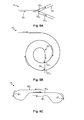
- Fig. 5B shows an embodiment of a part of an optical waveguide 11 operating as delay unit 10 1 to 10 M according to the present invention.
- the delay unit 10 1 to 10 M is part of the optical waveguide 11 and that this part of the optical waveguide 11 has the shape of a meander.
- the delay units 10 1 to 10 M can also have the shape of a spiral, wherein an inner segment 55 of the delay unit 10 1 to 10 M is lead to the outside by using a straight line 56 thereby crossing the other segments 57 1 , 57 2 at an angle of about 90°.
- An angle of 90° ensures that the delayed clock signal on the straight line 56 does not interfere with the more or less delayed clock signals on the other segments 57 1 , 57 2 .
- Fig. 5C shows another embodiment of an optical waveguide 11 operating as a delay unit 10 1 to 10 M according to the present invention.
- the delay unit 10 1 to 10 M can have the shape of a meander, wherein the delay unit 10 1 to 10 M has segments 60 1 , 60 2 that are parallel to each other and wherein the delay unit 10 1 to 10 M has other segments 61 that are round, thereby connecting the parallel segments 60 1 , 60 2 to each other.
- the radius of the other segments 61 can be equal to the distance between the two parallel segments 60 1 , 60 2 as shown in Fig. 4 .
- the diameter of the other segments can also be larger than the distance between the two parallel segments 60 1 , 60 2 as shown in Fig. 5C . If the other segment 61 has a radius that is larger than the distance between the two parallel segments, the optical power loss is further reduced.
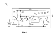
- Fig. 6 shows an embodiment of an opto-electronic flip-flop 12 1 to 12 N that can be used as an electronic clock generator.
- the opto-electronic flip-flop 12 1 to 12 N comprises several transistors 60 1 , 60 2 , 60 3 , 60 4 .
- the emitters of the transistors 60 1 , 60 2 are connected to a photodiode 61, which, for its part, is connected to a negative supply voltage, which can also be connected to ground.
- Data inputs D and D are connected to the base terminals of the transistors 60 1 , 60 2 .
- the collectors of the transistors 60 1 , 60 2 are each connected by means of a resistor 62 1 , 62 2 to a positive supply voltage.
- the photodiode 61 in this circuit is connected in such a manner that only minimal leakage current flows, as long as no light falls on the photodiode 61. As soon as light falls onto the photodiode 61, a photocurrent passes from an n-doped to a p-doped region of the photodiode. The intensity of the photocurrent is, in a good approximation, proportional to the luminous power of the laser pulse.
- Fig. 6 shows also a differential pair of transistors 60 3 , 60 4 which form a latch.
- the base terminals of this differential pair are connected crosswise to the collector terminals of the transistors 60 1 , 60 2 . That is to say, the base terminal of the transistor 60 3 is connected to the collector terminal of the transistor 60 1 .
- the base terminal of the transistor 60 4 is connected to the collector terminal of the transistor 60 2 .
- the collector terminal of the transistor 60 3 is connected to the collector terminal of the transistor 60 2 .
- the collector terminal of transistor 60 4 is also connected to the collector terminal of transistor 60 1 .
- the emitter terminals of the transistors 60 3 , 60 4 are connected via a current source 63 to a negative supply voltage, which can also be connected to ground.
- the zero-signal current of the latch generated by the current source 63 must be significantly smaller than the photocurrent which is generated by the photodiode 61. Only if this condition is fulfilled, can the photocurrent of the photodiode 61 exceeds the zero-signal current of the current source 63 and accordingly varies the logical status of the latch.
- the optically controlled D-flip-flop also called the opto-electronic flip-flop 12 1 , 12 2 to 12 N , illustrated here can be used for a plurality of applications.
- it is suitable for use in a high-precision clock generator that can be used i.e. within a sampling device 2 according to the present invention.
- a feedback loop In order to generate an electrical clock signal, of which the clock statuses provide the same length (duty cycle 50%), a feedback loop has also to be implemented.
- Fig. 6 shows also a delaying device 64.
- the delaying device 64 comprises two transistors 65 1 , 65 2 , a current source 66 and two resistors 67 1 , 67 2 .
- the two resistors 67 1 , 67 2 are each connected between a positive supply voltage and the collector of one of the transistors 65 1 , 65 2 as load resistors.
- the emitters of the transistors 65 1 , 65 2 are each connected to the current source 66, which is connected to a negative supply voltage, which can also be connected to ground.
- the base of the transistor 65 1 is connected to the base of the transistor 60 4 .
- the base of the transistor 65 2 is connected to the base of the transistor 60 3 .
- the collector of the transistor 65 1 is connected to the base of the transistor 60 1 as a feedback.
- the collector of the transistor 65 2 is connected to the base of the transistor 60 2 .
- Fig. 7 shows an embodiment of a simplified track-and-hold-unit 7 1 , 7 2 to 7 N .
- the simplified track-and-hold-unit 7 1 , 7 2 to 7 N has three input ports.
- An RF-signal is fed to the first input port 70, wherein a clock signal is fed to a second input port 71, wherein a clock-not-signal is fed to the third input port 72.
- the first input port of the track-and-hold-unit 7 1 to 7 N is connected to one end of a resistor 73, wherein the other end of the resistor 73 is connected to a supply voltage.
- the first input port 70 is also connected to a base of a transistor 74 and to a collector of another transistor 75.
- the collector of the transistor 74 is also connected to the supply voltage.
- the emitter of the transistor 74 is connected to a collector of a further transistor 76 and to one end of a capacitor 77, wherein the other end of the capacitor 77 is connected to a supply voltage that can be ground for example.
- the base of the further transistor 76 is connected to the second input port 71 of the simplified track-and-hold-unit 7 1 to 7 N , wherein the base of the other transistor 75 is connected to the third input port 72 of the simplified track-and-hold-unit 7 1 to 7 N .
- the emitters of the other transistor 75 and the further transistor 76 are connected together and to a current source 79.
- the third input port 72 of the simplified track-and-hold-unit 7 1 to 7 N can also be connected to a constant voltage source, if the voltage is lower than the logic "high” level of the electric clock signal and higher than the logic "low” level of the electrical clock signal, wherein the electrical clock signal is fed to the second input port 71. Otherwise, a clock-not-signal can be input to the third input port 72 too, wherein the clock-not-signal has a phase shift of 180° with respect to the electrical clock signal which is input to the second input port 71.
- the further transistor 76 is in a conducting state.
- the capacitor 77 is charged with a part of the RF-signal, wherein the part equals the RF-signal minus the voltage U BE of the transistor 74.
- the logic level of the electrical clock signal is "low” at the second input port 71 of the simplified track-and-hold-unit 7 1 to 7 N , the other transistor 75 is in a conducting state which ensures that the transistor 74 is not in a conducting state.
- the resistor 73 enhances this effect.
- Fig. 8 shows an embodiment of a chip structure carrying the sampling device 2 according to the present invention.
- the chip comprises a silicon wafer as a ground structure.
- the optical waveguide 11 comprising the optical power splitters 9 1 to 9 N-1 and the delay units 10 1 to 10 M are arranged on a first part 80 1 of the wafer.
- the optical waveguide 11 together with the aforementioned components are made of a layer which is transparent for the respective wavelength of the light source, i.e. germanium or SiO 2 . It should be mentioned that other materials that can be deposited on a wafer and that have a transparent structure can be used as well for creating the optical waveguide 11.
- the plurality of the track-and-hold-units 7 1 to 7 N and the opto-electronic flip-flops 12 1 to 12 N are arranged on a second part 80 2 of the wafer.
- the photodiode 61 within the opto-electronic flip-flop 12 1 to 12 N is preferably arranged at the changeover between the first part 80 1 and the second part 80 2 of the wafer.
- the components of the second part 80 2 are preferably made of SiGe. It should be clear that other materials can be used as well if they can be deposited on a wafer and if they are suitable for high-speed data rates.
- optical delay units 10 1 to 10 M it is also possible to delay the electrical RF-signal which is input at the first input port 4. This could be done in a limited range by a proper insertion of varactors, for example by insertion of voltage-dependent capacitors.
Landscapes
- Physics & Mathematics (AREA)
- General Physics & Mathematics (AREA)
- Optics & Photonics (AREA)
- Engineering & Computer Science (AREA)
- Microelectronics & Electronic Packaging (AREA)
- Nonlinear Science (AREA)
- Theoretical Computer Science (AREA)
- Optical Communication System (AREA)
Abstract
Description
- The invention relates to a sampling device which comprises a plurality of track-and-hold-units that are operated in a time-interleaved mode.
- The increasing need for wideband communication systems drives an increasing demand for suitable measurement systems. For analyzing those communication systems, the measurement systems need a really high bandwidth and a good jitter performance. In order to obtain a measurement system having such a good jitter performance, the whole clock tree has to be stabilized.
- The publication E. W Jacobs et al. "Optically clocked track-and-hold for high-speed, high-resolution analog-to-digital conversion" IEEE MWP '04, 2004, pages 190 - 192, describes a track-and-hold-unit that can be used within an analogue-to-digital-converter, wherein the track-and-hold-unit receives an optical clock. The track-and-hold-unit therefore comprises two photodiodes that are used for generating an electrical current which is fed into a diode circuit thereby turning off a lower current from two current sources. Whenever an optical pulse is received by the two photodiodes, a high frequency signal is kept constant at the output of the diode bridge.
- It is a drawback of the publication that the sampling rate is limited, because the necessary hold-times for the analog/digital-converter cannot be reduced anymore.
- It is therefore the object of the present invention to create a sampling device that has a very high sampling rate as well as a good jitter performance.
- This object is solved by the features of the
independent claim 1 relating to a sampling device. Any beneficial further developments of the invention are defined in the dependent claims. - The inventive sampling device comprises a first input port and a second input port, wherein an input-signal is fed to the first input port and wherein an optical clock signal is fed to the second input port. The sampling device further comprises a plurality of track-and-hold-units, wherein each of the plurality of the track-and-hold-units is connected to the first input port and wherein the plurality of the track-and-hold-units is also connected to the second input port through an optical waveguide in such a manner that the plurality of the track-and-hold-units operate in a time-interleaved mode. It is very advantageous that a plurality of track-and-hold-units are used and that a single optical clock signal can be forwarded to those plurality of track-and-hold-units, so that only one light source is needed. It is further beneficial that the plurality of the track-and-hold-units operate in a time-interleaved mode. This ensures that the input-signal is captured by the plurality of the track-and-hold-units at different times, thereby allowing each of the plurality of the track-and-hold-units to store a part of the input-signal for a longer time.
- It is also very advantageous if the optical waveguide comprises delay units, wherein the delay units delay the optical clock signal by a period of Δt=1/(N • fclk), wherein fclk is the frequency of the optical clock signal and wherein N is the number of the plurality of the track-and-hold-units. Therefore, each track-and-hold-unit has N times more time to hold a part of the input-signal for the following analogue-to-digital-conversion circuit, thereby increasing the sampling frequency by the factor of N.
- It is very advantageous if each delay unit is a part of the optical waveguide and if each delay unit has the shape of a meander and/or if each delay unit has segments that are parallel to each other and if each delay unit has other segments that connect the parallel segments to each other, wherein the other segments are round having a diameter that is equal or larger than the distance between the two parallel segments. The use of such delay units, that have the shape of a meander having parallel segments as well as the use of the other round segments connecting the parallel segments to each other, ensure that the power loss of the optical clock signal is minimized. However, no corners or other disadvantageous changeovers are used within the delay units.
- It is further beneficial if the delay unit is a part of the optical waveguide and if this part of the optical waveguide, which forms the delay unit, has the shape of a spiral, wherein an inner segment of the delay unit which is also an inner segment of the spiral is lead to the outside within a straight line, thereby crossing the other segments at an angle of about 90°. If an angle of 90° is maintained, it is possible that the optical clock signal in different segments of the optical waveguide can cross itself without interfering itself. Therefore, the optical waveguide can be applied very easily.
- It is also very advantageous, if the optical waveguide comprises N-1 optical power dividers, wherein N is the number of the plurality of the track-and-hold-units, wherein each optical power divider splits the optical waveguide into a first branch and a second branch, and/or if the ratio of the signal power at each branch can be selected by adjusting the divergency angle of the first branch and the divergency angle of the second branch with respect to an incoming signal line of the optical power divider. The use of such optical power dividers is very helpful, because the jitter performance is not degraded. It is also very useful, if the signal power at each branch can be adjusted, because it can be guaranteed that each of the plurality of the track-and-hold-units receives the same signal level.
- It is also very beneficial if the N-1 optical power dividers are connected in the structure of a binary tree whose root is located at the second input port and whose N terminal branches connect to the N track-and-hold units. The terminal branches are also the leaf nodes of the binary tree. It should be noted, that all kinds of binary trees can be used, like a perfect binary tree or a complete binary tree.
- Furthermore, it is advantageous, if at least one delay unit is arranged within the second branch of each of the N-1 optical power dividers. This ensures that every track-and-hold-unit operates at a different time, so that every track-and-hold-unit captures a different part of the input-signal.
- It is further beneficial if the depths of all branches of the tree-structure comprising all descendants of the first optical power divider are the same and/or if the number of the delay units that are ranged within the second branch of every optical power divider equals the number of the track-and-hold-units that are connected as descendants to that respective branch and/or if no delay unit is arranged within the first branch of every optical power divider. This ensures that all N-1 optical power dividers are arranged symmetrically so that the only difference in the various branches is the number of the delay units. This allows that the signal power can be adjusted more easily within the N-1 optical power dividers, so that each of the plurality of the track-and-hold-units receives approximately the same signal level.
- It is also very advantageous if the sampling device comprises a plurality of opto-electronic flip-flops, wherein each of the plurality of the opto-electronic flip-flops transforms the optical clock signal into an electrical clock signal, wherein each of the plurality of the opto-electronic flip-flops connects each of the track-and-hold-units to the optical waveguide. This ensures that the electrical clock signal has a duty cycle of approximately 50%, wherein the light pulses of the optical clock signal are much smaller.
- It is also very beneficial if the optical waveguide is made of a layer of germanium or SiO2 and/or if the optical waveguide, the optical power splitters and the delay units are made of germanium or SiO2 and if they are arranged on a first part of the wafer and if the plurality of the track-and-hold-units and the opto-electronic flip-flops are made of SiGe and if they are arranged on a second part of the wafer and if the opto-electric flip-flop comprises a photodiode that is arranged in between the two parts of the wafer. This ensures that the wafer can be used by the optic elements as well by the electronic elements. This allows that all of the aforementioned components can be integrated within a single chip, thereby reducing the unit costs.
- It is further beneficial if a mode locked laser is used to generate the optical clock signal and if the mode locked laser is connected through an optical fiber to the second input port. A mode locked laser has very good jitter performance as well as an output power on the order of 30 mW.
- Different embodiments of the present invention are described exemplary in the following with reference to the description. This is done by the way of example only, without limitation. Identical elements have the same reference signs. The figures in the drawings show:
- Fig. 1
- a high speed sampling unit comprising an embodiment of the sampling device according to the present invention and a plurality of track-and-hold-units which are operated in a time-interleaved mode;
- Fig. 2
- a sampling device according to an embodiment of the present invention;
- Fig. 3
- a simplified layout of the sampling device according to an embodiment of the present invention;
- Fig. 4
- a simplified layout of the sampling device according to another embodiment of the present invention;
- Fig. 5A
- an embodiment of an optical power divider according to the present invention;
- Fig. 5B
- an embodiment of an optical waveguide operating as delay unit according to the present invention;
- Fig. 5C
- another embodiment of an optical waveguide operating as delay unit according to the present invention;
- Fig. 6
- an embodiment of an opto-electronic flip-flop used as an electronic clock generator;
- Fig. 7
- an embodiment of a simplified track and hold unit; and
- Fig. 8
- an embodiment of a simplified chip structure carrying the sampling device according to the present invention.
-
Fig. 1 shows a high-speed sampling unit 1 comprising thesampling device 2, which in turn comprises track-and-hold-units speed sampling unit 1 can be integrated within a single chip or ASIC. However, it is also possible that thesampling device 2 can be integrated on a chip of its own while the analog/digital-converters 31, 32 to 3N are located on separate chips. It should be noted, that the analog/digital-converters 31, 32 to 3N are only incorporated withinFig. 1 for a better understanding and that they are not a necessary part of the invention. Thesampling device 2 further comprises afirst input port 4 and asecond input port 5. An electrical input-signal, i.e. a RF-signal, is fed to thefirst input port 4. The RF-signal is a high-frequency signal having a bandwidth of approximately up to 30 GHz and above. - The RF-signal is then amplified by at least one
amplifier 6. However, if N is small, for example four or eight the RF-signal does not need to be amplified. The amplification factor of the at least oneamplifier 6 is preferably adjustable. The amplified RF-signal is then fed to each of a plurality of the track-and-hold-units - Furthermore, the high-
speed sampling unit 1 comprises anoptical clock source 8. The optical clock source is preferably a mode lockedlaser 8. The mode lockedlaser 8 is difficult to integrate within a chip together with the other components of the high-speed sampling unit 1. The mode lockedlaser 8 generates an optical clock signal having a frequency fclk of, for example, 10 GHz. The energy for each pulse exceeds for example 3 pJ and the timing jitter is smaller than 20 fs RMS. - The
sampling device 2 preferably comprises the at least oneamplifier 6, the plurality of the track-and-hold-units optical power divider 9 and at least onedelay unit - The mode locked
laser 8 is connected to the second input port by using an optical fiber. Within thesampling device 2 which can also be within a chip, anoptical waveguide 11 is used to lead the optical clock signal to each of the plurality of the track-and-hold-units units - The
second input port 5 which is connected to theoptical waveguide 11 is connected to a firstoptical power divider 9. A first branch of the first optical power divider is connected to the first track-and-hold-unit 71. A second branch of the firstoptical power divider 9 is connected to afirst delay unit 101. Thefirst delay unit 101 is further connected to a anotherdelay unit 10M, wherein M ≥ 1 and M ∈. Within the
first delay unit 101 there is also another optical power divider which splits up the optical clock signal into a signal that is fed to the second track-and-hold-unit 72. Another signal of the another optical power divider is then fed to the other track-and-hold-units 7N, wherein N ≥ 2 and N ∈.
- It should also be noted that all branches which extend from every
optical power divider 9 still belong to theoptical waveguide 11. - Every
delay unit 101 to 10M delays the optical clock signal by a period Δt=1/ (N • fclk), wherein fclk is the frequency of the optical clock signal. If the number for N is three for example, eachdelay unit 101 to 10M delays the optical clock signal by the factor of 1/3 period. This means that the track-and-hold-units - Each of the plurality of the track-and-hold-
units flops flops units optical waveguide 11. The plurality of the opto-electronic flip-flops flops units units sampling device 2. - The output of each of the plurality of the track-and-hold-
units amplifier amplifiers -
Fig. 2 shows asampling device 2 according to the present invention. Thesampling device 2 comprises a plurality of track-and-hold-units units delay units 101 to 10M. Eachdelay unit optical waveguide 11 which is explained in detail below. - The
optical waveguide 11 further comprises N-1optical power dividers 91 to 9N-1 wherein N is the interleaving factor as well as the number of the plurality of the track-and-hold-units optical power divider 91 to 9N-1 splits theoptical waveguide 11 into a first branch and into a second branch. If theoptical waveguide 11 is nearly lossless, each branch should get half the incoming optical power. In practice, the optical waveguide may have substantial losses, whereby a larger attenuation will occur on a branch with a large delay compared to a branch with a small delay. In this case, it is preferable to provide more power to the branch with a large delay so that the power at the output of each branch will be substantially equal. The ratio of the signal power at each branch can be selected by adjusting the divergency angle of the first branch and the divergency angle of the second branch with respect to the incoming signal line of the respectiveoptical power divider 91 to 9N-1. These details will also be explained below. - The ratio of the signal power of all N-1
optical power dividers 91 to 9N-1 is adjusted in such a way that the signal power at each end node of theoptical waveguide 11 or at each of the plurality of the track-and-hold-units optical power dividers 91 to 9N-1 has to be adjusted in such a way that the signal power should be the same at the input port of the plurality of the opto-electronic flip-flops flops units flops 121 to 12N are arranged in front of the track-and-hold-units -
Fig. 2 describes a symmetrical tree-structure of theoptical waveguide 11. This means that the depth of all branches of the tree-structure is the same, wherein the tree-structure comprises all descendants of the firstoptical power divider 91. The descendants comprise the furtheroptical power dividers 92 to 9N-1 as well as the plurality of thedelay units optical power divider 91. The firstoptical power divider 91 is thereby connected to thesecond input port 5. In the embodiment ofFig. 2 the depth of the tree-structure is three. - Furthermore, the number of the
delay units 101 to 10M arranged within a second branch of everyoptical power divider 91 to 9N-1 equals the number of the track-and-hold-units optical divider 91 comprises fourdelay units 101. This is indicated by the number "4" before Δt. However, the second branch of the firstoptical divider 91 is connected to four track-and-hold-units optical divider 92. The second branch of the secondoptical divider 92 is connected to two track-and-hold-units delay units 102 are incorporated within the second branch of the secondoptical power divider 92. - A branch is a line segment of the
optical waveguide 11 that extends from the output of each of theoptical power dividers 91 to 9N-1 and ends at the input of the descendantoptical power divider 91 to 9N-1 or at the input port of the opto-electronic flip-flop 121 to 12N or at the input port of the track-and-hold-unit delay unit 101 to 10M can be incorporated. As described in detail below thedelay unit 101 to 10M is an integral part of theoptical waveguide 11 having a special wiring. - In the embodiment of
Fig. 2 according to the present invention nodelay units 101 to 10M are arranged within the first branch of everyoptical power divider 91 to 9N-1. It is clear that the optical clock signal, which is fed to the first track-and-hold-unit 71, is only delayed by the length of theoptical waveguide 11 from thesecond input port 5 to the respective input port of the opto-electronic flip-flop 121 of the first track-and-hold-unit 71. However, the optical clock signal of the second track-and-hold-unit 72 is delayed by one delay unit by a period Δt=1/(N • fclk). If the period has a length of 100 ps the optical clock signal for the second track-and-hold-unit 72 is delayed by 12.5 ps. It is also clear that the clock signal for the third track-and-hold-unit 73 is delayed by 25 ps compared to the clock signal fed to the first track-and-hold-unit 71. - When calculating the division ratio of the
optical power dividers 91 to 9N-1 the amount of the descendant branches have to be taken into account comprising the amount of thedescendant delay units 91 to 9N-1. For example, the first branch of the firstoptical power divider 91 comprises fourdescendant delay units 101 to 10M, wherein the second branch of the firstoptical power divider 91 comprises eightdelay units 101 to 10M. Putting all this information together, the division ratio of all theoptical power dividers 91 to 9N-1 can be calculated, so that the input signal level is the same for all of the plurality of the opto-electronic flip-flop 121 to 12N or for the plurality of the track-and-hold-units - However, it should be clear that the tree-structure described above can also be brought forward to a
sampling device 2 having more or less track-and-hold-units Fig. 2 . - There are also other tree-structures possible that do not have to be symmetrical. However, all tree-structures have in common that the root-node is connected to the
second input port 5 and that a plurality of end-nodes are connected to the plurality of the track-and-hold-units flops 121 to 12N. The at least onedelay unit 101 to 10M delays the optical clock signal in such a manner that each of the plurality of the track-and-hold-units - As already mentioned other tree-structures for the
optical waveguide 11 can also be used. For example, the N-1optical power dividers 91 to 9N-1 can be connected in series so that eachoptical power divider 91 to 9N is connected to the second branch of a respective parentoptical power divider 91 to 9N-1, wherein the firstoptical power divider 91 is connected to thesecond input port 5 and wherein the first branch of each of the N-1optical power dividers 91 to 9N-1 is connected to the respective track-and-hold-unit Fig. 1 for example. - Furthermore, one
delay unit 101 to 10M is arranged within the second branch of each of the N-1optical power dividers 91 to 9N-1. This kind of tree-structure can preferably be used if the number of the track-and-hold-units optical power divider 91 can easily be adjusted. However, if there are, for example, 32 track-and-hold-units optical power divider 91 should have a division ratio of at least 1:32 which is difficult to obtain. - The plurality of the track-and-hold-
units amplifiers 131 to 13N, wherein the output of the plurality of theamplifiers 131 to 13N is preferably also the output of the chip. -
Fig. 3 shows a simplified layout of thesampling device 2 according to an embodiment of the present invention. As already mentioned an RF-signal is fed to thefirst input port 4. Within an RF-distribution circuit 30, the RF-signal is split into N individual signals which are fed to the plurality of the track-and-hold-units distribution circuit 30 comprisesseveral amplifiers 6 for amplifying each of the individual RF-signals. It should be noted that the RF-distribution circuit 30 is matched with respect to thefirst input port 4. - Furthermore, as already described, an optical clock signal is fed to the
second input port 5. This optical clock signal is preferably generated by a mode lockedlaser 8. The optical clock signal is then split up by a firstoptical power divider 91 which is part of theoptical waveguide 11. - In order to simplify the arrangement, the plurality of opto-electronic flip-
flops 121 to 12N which transform an optical clock signal into an electrical clock signal are not shown withinFig. 3 . - The plurality of the
delay units 101 to 10M are also shown within the layout ofFig. 3 . Thedelay units 101 to 10M which are part of theoptical waveguide 11 have the shape of a meander. It has to be noted that the corners of the meander of thedelay units 101 to 10M are illustrated disproportionately. As described below, the meander structure has only round segments which connect the parallel segments to each other. The meander structure thereby increases the light length with respect to the typically straight lines of theoptical waveguide 11. It can clearly be seen that the optical clock signal for the first track-and-hold-unit 71 does not travel through anydelay unit 101 to 10M. The optical clock signal for the last track-and-hold-unit 7N travels through N-1delay units 101 to 10M. - If the clock signal has a period of 100 ps each output port is delayed to the respective adjacent output port by 12.5 ps. Because a mode locked laser has a very good jitter performance, the difference between the delay times of each output port is constant.
-
Fig. 4 shows a simplified layout of thesampling device 2 according to another embodiment of the invention. The interleaving factor N is higher inFig. 4 compared to the interleaving factor inFig. 2 . The interleaving factor N equals 16 so that there are also 16 track-and-hold-units first input port 4. The RF-signal is then split into two signal paths, wherein each signal path comprises anamplifier 6. Each signal path is then further split, so that a part of the RF-signal which is fed to thefirst input port 4 also applies at the input port of each of the plurality of the track-and-hold-units -
Fig. 4 also shows thesecond input port 5 which is connected through an optical fiber to the mode lockedlaser 8. Theinput port 5 consists of a grating, which couples the incident light into theoptical waveguide 11. This ensures that as much power of the light pulses as possible can be injected into theoptical waveguide 11. Other forms which also reduce the power loss of the optical clock signal at thesecond input port 5 are also suitable. - As already described, the
optical waveguide 11 is split by firstoptical power divider 91 into a first branch and a second branch. As already described a plurality ofdelay units 101 to 10M are formed within theoptical waveguide 11. Eachdelay unit 101 to 10M is separated from theadjacent delay unit 101 to 10M as indicated by a dotted line. The number of thedelay units 101 to 10M which are arranged within the second branch of the firstoptical power divider 91 also equals the number of the track-and-hold-units units optical power divider 91. Thus, there are eight delay units inserted within the second branch. The same also applies for example for the secondoptical power divider 92. In this case there are four track-and-hold-units optical divider 92. Therefore, the second branch of the secondoptical power divider 92 comprises fourdelay units 101 to 10M. On the other hand, as already mentioned, the first branch of everyoptical power divider 91 to 9N-1 does not comprise anydelay unit 101 to 10M. -
Fig. 4 also shows the plurality of the opto-electronic flip-flops 121 to 12N. Each of the opto-electronic flip-flops 121 to 12N is arranged at an input port of a track-and-hold-units flop 121 to 12N transforms an optical clock signal to an electronic clock signal that is fed to the respective track-and-hold-unit flop 121 to 12N. This goal is achieved by a suitable angle between the first and the second branch of each of theoptical power dividers 91 to 9N-1 with respect to the input port of theoptical power divider 91 to 9N-1. -
Fig. 5A shows a simplified embodiment of theoptical power divider 91 to 9N-1. It can be seen that theoptical power divider 91 to 9N-1 has oneincoming signal line 50 which is part of theoptical waveguide 11. Theincoming signal line 50 is split into a first branch 511 and a second branch 512. The ratio of the signal power at each branch 511, 512 can be selected by adjusting the divergency angle 521 of the first branch and the divergency angle 522 of the second branch 512 with respect to theincoming signal line 50 of theoptical power divider 91 to 9N-1. If the starting point of the first branch 511 and the second branch 512 is in the middle of the incoming signal line and if both divergency angles are 45°, theoptical power divider 91 to 9N-1 divide the optical clock signal into two clock signals both having the same signal power level. - Furthermore, a
corner 53 which connects the first branch 511 to the second branch 512 can be slid along the width of theincoming signal line 50 to further adjust the division ratio which allows buildingoptical power dividers 91 to 9N-1 that have a very high division ratio of for example 1:30 or above. Those kind ofoptical power dividers 91 to 9N-1 can be used if an asymmetrical tree-structure of theoptical waveguide 11 should be realized. - The first branch 511 and the second branch 512 shown in the embodiment of
Fig. 5A have a smaller width than theincoming signal line 50. It should be clear that the first branch 511 and the second branch 512 can also have a width that equals the width of theincoming signal line 50 or they can have a width that is larger than the one of theincoming signal line 50. - As already mentioned, the
incoming signal line 50 as well as the first branch 511 and the second branch 512 of eachoptical power divider 91 to 9N-1 are part of theoptical waveguide 11 and are therefore made of a transparent layer of germanium or SiO2. Theoptical power divider 91 to 9N-1 as well as the wholeoptical waveguide 11 can easily be structured on a common wafer. Furthermore it is also possible to create an optical power divider that has more than two branches. -
Fig. 5B shows an embodiment of a part of anoptical waveguide 11 operating asdelay unit 101 to 10M according to the present invention. WithinFig. 3 andFig. 4 it is shown that thedelay unit 101 to 10M is part of theoptical waveguide 11 and that this part of theoptical waveguide 11 has the shape of a meander. However, thedelay units 101 to 10M can also have the shape of a spiral, wherein aninner segment 55 of thedelay unit 101 to 10M is lead to the outside by using astraight line 56 thereby crossing the other segments 571, 572 at an angle of about 90°. An angle of 90° ensures that the delayed clock signal on thestraight line 56 does not interfere with the more or less delayed clock signals on the other segments 571, 572. As already mentioned it has to be assured that no corners are used. - The larger the radius of all parts of the spiral shaped
delay units 101 to 10M is, the more can the loss of the optical power be reduced. -
Fig. 5C shows another embodiment of anoptical waveguide 11 operating as adelay unit 101 to 10M according to the present invention. As mentioned above, thedelay unit 101 to 10M can have the shape of a meander, wherein thedelay unit 101 to 10M has segments 601, 602 that are parallel to each other and wherein thedelay unit 101 to 10M hasother segments 61 that are round, thereby connecting the parallel segments 601, 602 to each other. The radius of theother segments 61 can be equal to the distance between the two parallel segments 601, 602 as shown inFig. 4 . However, the diameter of the other segments can also be larger than the distance between the two parallel segments 601, 602 as shown inFig. 5C . If theother segment 61 has a radius that is larger than the distance between the two parallel segments, the optical power loss is further reduced. -
Fig. 6 shows an embodiment of an opto-electronic flip-flop 121 to 12N that can be used as an electronic clock generator. The opto-electronic flip-flop 121 to 12N comprises several transistors 601, 602, 603, 604. The emitters of the transistors 601, 602 are connected to aphotodiode 61, which, for its part, is connected to a negative supply voltage, which can also be connected to ground. Data inputs D andD are connected to the base terminals of the transistors 601, 602. The collectors of the transistors 601, 602 are each connected by means of aresistor - The
photodiode 61 in this circuit is connected in such a manner that only minimal leakage current flows, as long as no light falls on thephotodiode 61. As soon as light falls onto thephotodiode 61, a photocurrent passes from an n-doped to a p-doped region of the photodiode. The intensity of the photocurrent is, in a good approximation, proportional to the luminous power of the laser pulse. -
Fig. 6 shows also a differential pair of transistors 603, 604 which form a latch. The base terminals of this differential pair are connected crosswise to the collector terminals of the transistors 601, 602. That is to say, the base terminal of the transistor 603 is connected to the collector terminal of the transistor 601. The base terminal of the transistor 604 is connected to the collector terminal of the transistor 602. Moreover, the collector terminal of the transistor 603 is connected to the collector terminal of the transistor 602. The collector terminal of transistor 604 is also connected to the collector terminal of transistor 601. The emitter terminals of the transistors 603, 604 are connected via acurrent source 63 to a negative supply voltage, which can also be connected to ground. As a result of the crosswise wiring, a positive feedback is generated, and accordingly, the logical status of the latch is maintained. In this context, the zero-signal current of the latch generated by thecurrent source 63 must be significantly smaller than the photocurrent which is generated by thephotodiode 61. Only if this condition is fulfilled, can the photocurrent of thephotodiode 61 exceeds the zero-signal current of thecurrent source 63 and accordingly varies the logical status of the latch. - The optically controlled D-flip-flop, also called the opto-electronic flip-
flop sampling device 2 according to the present invention. In order to generate an electrical clock signal, of which the clock statuses provide the same length (duty cycle 50%), a feedback loop has also to be implemented. -
Fig. 6 shows also adelaying device 64. The delayingdevice 64 comprises twotransistors current source 66 and two resistors 671, 672. The two resistors 671, 672 are each connected between a positive supply voltage and the collector of one of thetransistors transistors current source 66, which is connected to a negative supply voltage, which can also be connected to ground. The base of thetransistor 651 is connected to the base of the transistor 604. The base of thetransistor 652 is connected to the base of the transistor 603. Moreover, the collector of thetransistor 651 is connected to the base of the transistor 601 as a feedback. Similarly, the collector of thetransistor 652 is connected to the base of the transistor 602. -
Fig. 7 shows an embodiment of a simplified track-and-hold-unit unit first input port 70, wherein a clock signal is fed to asecond input port 71, wherein a clock-not-signal is fed to thethird input port 72. The first input port of the track-and-hold-unit 71 to 7N is connected to one end of aresistor 73, wherein the other end of theresistor 73 is connected to a supply voltage. Furthermore, thefirst input port 70 is also connected to a base of atransistor 74 and to a collector of anothertransistor 75. The collector of thetransistor 74 is also connected to the supply voltage. The emitter of thetransistor 74 is connected to a collector of afurther transistor 76 and to one end of acapacitor 77, wherein the other end of thecapacitor 77 is connected to a supply voltage that can be ground for example. The base of thefurther transistor 76 is connected to thesecond input port 71 of the simplified track-and-hold-unit 71 to 7N, wherein the base of theother transistor 75 is connected to thethird input port 72 of the simplified track-and-hold-unit 71 to 7N. The emitters of theother transistor 75 and thefurther transistor 76 are connected together and to a current source 79. - However, instead of connecting the
third input port 72 of the simplified track-and-hold-unit 71 to 7N to a clock-not-signal, thethird input port 72 can also be connected to a constant voltage source, if the voltage is lower than the logic "high" level of the electric clock signal and higher than the logic "low" level of the electrical clock signal, wherein the electrical clock signal is fed to thesecond input port 71. Otherwise, a clock-not-signal can be input to thethird input port 72 too, wherein the clock-not-signal has a phase shift of 180° with respect to the electrical clock signal which is input to thesecond input port 71. - If the logic level of the electrical clock signal is "high", the
further transistor 76 is in a conducting state. Thus, thecapacitor 77 is charged with a part of the RF-signal, wherein the part equals the RF-signal minus the voltage UBE of thetransistor 74. If the logic level of the electrical clock signal is "low" at thesecond input port 71 of the simplified track-and-hold-unit 71 to 7N, theother transistor 75 is in a conducting state which ensures that thetransistor 74 is not in a conducting state. Theresistor 73 enhances this effect. -
Fig. 8 shows an embodiment of a chip structure carrying thesampling device 2 according to the present invention. The chip comprises a silicon wafer as a ground structure. Furthermore, theoptical waveguide 11 comprising theoptical power splitters 91 to 9N-1 and thedelay units 101 to 10M are arranged on a first part 801 of the wafer. Theoptical waveguide 11 together with the aforementioned components are made of a layer which is transparent for the respective wavelength of the light source, i.e. germanium or SiO2. It should be mentioned that other materials that can be deposited on a wafer and that have a transparent structure can be used as well for creating theoptical waveguide 11. - On the other side the plurality of the track-and-hold-
units 71 to 7N and the opto-electronic flip-flops 121 to 12N are arranged on a second part 802 of the wafer. It should be noted that thephotodiode 61 within the opto-electronic flip-flop 121 to 12N is preferably arranged at the changeover between the first part 801 and the second part 802 of the wafer. The components of the second part 802 are preferably made of SiGe. It should be clear that other materials can be used as well if they can be deposited on a wafer and if they are suitable for high-speed data rates. - Instead of using the
optical delay units 101 to 10M it is also possible to delay the electrical RF-signal which is input at thefirst input port 4. This could be done in a limited range by a proper insertion of varactors, for example by insertion of voltage-dependent capacitors. - The invention is not restricted to the exemplary embodiment presented. All of the features described above or illustrated in the drawings can be advantageously combined with one another as required within the scope of the invention. Other transistors, such as PNP bipolar transistors, NMOS or PMOS transistors or even other FET transistors can be used instead of NPN transistors. Other light sources instead of a mode locked laser can be used, such as stroke lamps, LEDs or other kind of lasers, such as semiconductor lasers. A semiconductor laser might be integrated on the same chip if layers of a III-V-semiconductor, such as InGaAs is applied on the Si-substrate by MBE for example.
Claims (17)
- A sampling device (2) comprising a first input port (4) and a second input port (5),
wherein an input-signal is fed to the first input port (4) and wherein an optical clock signal is fed to the second input port (5),
characterized in that,
the sampling device (2) comprises a plurality of track and hold units (71, 72, 7N), wherein each of the plurality of track and hold units (71, 72, 7N) is connected to the first input port (4) and
that the plurality of track and hold units (71, 72, 7N) is connected to the second input port (5) through an optical waveguide (11) in such a manner that the plurality of track and hold units (71, 72, 7N) operate in a time-interleaved mode. - A sampling device according to claim 1,
characterized in that,
the optical waveguide (11) is arranged in a tree-structure, wherein a root-node is connected to the second input port (5) and wherein each of a plurality of end-nodes is connected to one of the track and hold units (71, 72, 7N), wherein the optical waveguide (11) comprises at least one delay unit (101, 102, 10M) that delays the optical clock signal so that each of the plurality of track and hold units (71, 72, 7N) captures the RF-signal at a different time. - A sampling device according to claim 2,
characterized in that,
each delay unit (101, 102, 10M) delays the optical clock signal by a period Δt = 1/(N • fclk), wherein N is the number of the plurality of the track and hold units (71, 72, 7N) and wherein fclk is the frequency of the optical clock signal. - A sampling device according to claim 2 or 3,
characterized in that,
each delay unit (101, 102, 10M) is a part of the optical waveguide (11) and that this part of the optical waveguide (11) has the shape of a meander and/or
that each delay unit (101, 102, 10M) has segments (601, 602) that are parallel to each other and that the delay unit (101, 102, 10M) has other segments (61) that connect the parallel segments (601, 602) to each other, wherein the other segments (61) are round having a diameter that is equal or larger than the distance between the two parallel segments (601, 602). - A sampling device according to claim 2 to 4,
characterized in that,
each delay unit (101, 102, 10M) is a part of the optical waveguide (11) and that this part of the optical waveguide (11) has the shape of a spiral, wherein an inner segment (55) of the delay unit (101, 102, 10M) is lead to the outside within a straight line (56) thereby preferably crossing other segments (571, 572) of the spiral at an angle of about 90 degree. - A sampling device according to claim 2 to 5,
characterized in that,
the optical waveguide (11) comprises N-1 optical power dividers (9; 91, 92, 9N-1) wherein N is the number of the plurality of the track and hold units (71, 72, 7N), wherein each optical power divider (9; 91, 92, 9N-1) splits the optical waveguide (11) into a first branch (511) and a second branch (512). - A sampling device according to claim 6,
characterized in that,
that the ratio of the signal power at each branch (511, 512) can be selected by adjusting the divergency angle of the first branch (511) and the divergency angle of the second branch (512) with respect to an incoming signal line (50) of the optical power divider (9; 91, 92, 9N-1). - A sampling device according to claim 7,
characterized in that,
that the ratio of the signal power of all N-1 optical power dividers (9; 91, 92, 9N-1) is adjusted in such a way that the signal power at each end-node or at each of the plurality of track and hold units (71, 72, 7N) is approximately the same. - A sampling device according to any of the claims 6 to 8,
characterized in that,
the N-1 optical power dividers (9; 91, 92, 9N-1) are connected in series so that each optical power divider (9; 91, 92, 9N-1) is connected to the second branch (512) of a respective parent optical power divider (9; 91, 92, 9N-1) and that the first optical power divider (9; 91) is connected to the second input port (5) and that the first branch (511) of the N-1 optical power dividers (9; 91, 92, 9N-1) is connected to the respective track and hold unit (71, 72, 7N). - A sampling device according to any of the claims 6 to 9,
characterized in that,
one delay unit (101, 102, 10M) is arranged within the second branch (512) of each of the N-1 optical power dividers (9; 91, 92, 9N-1). - A sampling device according to claim 6 to 8,
characterized in that,
a depth of all branches (511, 512) of the tree-structure comprising all descendants of the first optical power divider (9; 91) is the same and/or
that the number of delay units (101, 102, 10M) arranged within the second branch (512) of every optical power divider (9; 91, 92, 9N-1) equals the number of the track and hold units (71, 72, 7N) that are connected as descendants to that respective branch (512) and/or
that no delay unit (101, 102, 10M) is arranged within the first branch (511) of every optical power divider (9; 91, 92, 9N-1). - A sampling device according to claim 6 to 8 or claim 11,
characterized in that,
the N-1 optical power dividers (9; 91, 92, 9N-1) are connected in the structure of a binary tree whose root is located at the second input port (5) and whose N terminal branches (511, 512) connect to the N track-and-hold units (71, 72, 7N). - A sampling device according to any of the preceding claims,
characterized in that,
the sampling device (2) comprises a plurality of opto-electronic flip-flops (121, 122, 12N), wherein each of the plurality of the opto-electronic flip-flops (121, 122, 12N) transforms the optical clock signal into an electrical clock signal, wherein each of the plurality of the opto-electronic flip-flops (121, 122, 12N) connects each of the track and hold units (71, 72, 7N) to the optical waveguide (11) and/or wherein the electrical clock signal has a duty cycle of approximately 50%. - A sampling device according to claim 13,
characterized in that,
each of the plurality of track and hold units (71, 72, 7N) captures a part of the input-signal at the rising or falling edge of the respective optical clock signal or the respective transformed electrical clock signal for the duration of one clock period and/or
that the maximum frequency of the optical clock signal is equal to a maximum sampling frequency of a plurality of analog/digital-converters (31, 32, 3N) wherein each of the analog/digital-converters (31, 32, 3N) is connected to one of the plurality of the track and hold units (71, 72, 7N). - A sampling device according to claim 13 or 14 and 3 and 6,
characterized in that,
the optical waveguide (11) is made of a layer of germanium or SiO2 and/or
that the optical waveguide (11), the optical power splitters (9; 91, 92, 9N-1) and the delay units (101, 102, 10M) are made of germanium or SiO2 and are arranged on a first part (801) of a wafer and that the plurality of track and hold units (71, 72, 7N) and the opto-electronic flip-flops (121, 122, 12N) are made of SiGe heterojunction bipolar transistors and are arranged on a second part (802) of the wafer and that the opto-electronic flip-flops (121, 122, 12N) comprise a photodiode that is placed between the two parts (801, 802) of the wafer. - A sampling device according to any of the preceding claims,
characterized in that,
a mode locked laser (88) is used to generate the optical clock signal and that the mode locked laser (8) is connected with an optical fiber to the second input unit (5). - A sampling device according to claim 13,
characterized in that,
the opto-electronic flip-flop (101, 102, 10M) comprises a differential pair of first transistors (601, 602) and two load resistors (621, 622),
that the load resistors (621, 622) are connected between a supply voltage terminal and collectors of the first transistors (601, 602), and
that emitters of the first transistors (601, 602) are connected to the photodiode (61) and/or
that the opto-electronic flip-flop (101, 102, 10M) comprises a differential pair of second transistors (603, 604) and a first current source (63),
that the first current source (63) is connected between emitters of the second transistors (603, 604),
that base terminals of the second transistors (603, 604) are connected crosswise to collectors of the second transistors (603, 604), and
that the collectors of the second transistors (603, 604) are each connected to a collector of the first transistors (601, 602) and/or
that the opto-electronic flip-flop (101, 102, 10M) comprises a differential pair of third transistors (651, 652), two load resistors (671, 672) and a second current source (66),
that the load resistors (671, 672) are connected between a supply voltage terminal and collectors of the third transistors (651, 652),
that emitters of the third transistors (651, 652) are connected to the second current source (66), and
that base terminals of the third transistors (651, 652) are connected to at least one output (Q,Q ) of the opto-electronic flip-flop (101, 102, 10M).
Priority Applications (4)
| Application Number | Priority Date | Filing Date | Title |
|---|---|---|---|
| EP12167613.4A EP2660821B8 (en) | 2012-04-30 | 2012-05-11 | Sampling device with time-interleaved optical clocking |
| CN201380022685.3A CN104272395B (en) | 2012-04-30 | 2013-04-23 | Sampling apparatuses using the optics timing of time interleaving |
| US14/398,123 US9355742B2 (en) | 2012-04-30 | 2013-04-23 | Sampling device with time-interleaved optical clocking |
| PCT/EP2013/058362 WO2013164221A1 (en) | 2012-04-30 | 2013-04-23 | Sampling device with time-interleaved optical clocking |
Applications Claiming Priority (2)
| Application Number | Priority Date | Filing Date | Title |
|---|---|---|---|
| EP12166132 | 2012-04-30 | ||
| EP12167613.4A EP2660821B8 (en) | 2012-04-30 | 2012-05-11 | Sampling device with time-interleaved optical clocking |
Publications (3)
| Publication Number | Publication Date |
|---|---|
| EP2660821A1 true EP2660821A1 (en) | 2013-11-06 |
| EP2660821B1 EP2660821B1 (en) | 2018-10-31 |
| EP2660821B8 EP2660821B8 (en) | 2018-12-26 |
Family
ID=46062127
Family Applications (1)
| Application Number | Title | Priority Date | Filing Date |
|---|---|---|---|
| EP12167613.4A Active EP2660821B8 (en) | 2012-04-30 | 2012-05-11 | Sampling device with time-interleaved optical clocking |
Country Status (4)
| Country | Link |
|---|---|
| US (1) | US9355742B2 (en) |
| EP (1) | EP2660821B8 (en) |
| CN (1) | CN104272395B (en) |
| WO (1) | WO2013164221A1 (en) |
Cited By (3)
| Publication number | Priority date | Publication date | Assignee | Title |
|---|---|---|---|---|
| US20150003833A1 (en) * | 2013-06-28 | 2015-01-01 | Rohde & Schwarz Gmbh & Co. Kg | Optoelectronic circuit and a method for the transmission of an optical clock signal |
| WO2017069843A1 (en) * | 2015-10-23 | 2017-04-27 | Raytheon Company | Precision clock enabled time-interleaved data conversion |
| WO2019015724A1 (en) * | 2017-07-17 | 2019-01-24 | Universität Paderborn | FOLLOW-HOLD CIRCUIT |
Families Citing this family (7)
| Publication number | Priority date | Publication date | Assignee | Title |
|---|---|---|---|---|
| US9385893B2 (en) * | 2014-01-23 | 2016-07-05 | Avago Technologies General Ip (Singapore) Pte. Ltd. | Modular low power serializer-deserializer |
| US9461743B1 (en) * | 2014-07-16 | 2016-10-04 | Rockwell Collins, Inc. | Pulse to digital detection circuit |
| EP3151245B8 (en) * | 2015-10-01 | 2019-10-23 | Rohde & Schwarz GmbH & Co. KG | Sampling device |
| FR3059438A1 (en) * | 2016-11-30 | 2018-06-01 | Stmicroelectronics Sa | CLOCK SIGNAL GENERATOR |
| CN108183380B (en) * | 2018-01-05 | 2020-02-18 | 中国科学院半导体研究所 | Integrated optoelectronic oscillator |
| JP2021044638A (en) * | 2019-09-09 | 2021-03-18 | 株式会社東芝 | Electronic circuit |
| CN110806852B (en) * | 2019-10-31 | 2020-05-26 | 太原理工大学 | An All-optical True Random Number Generator Based on the Principle of Feedback Interference |
Citations (3)
| Publication number | Priority date | Publication date | Assignee | Title |
|---|---|---|---|---|
| EP1279974A2 (en) * | 2001-07-23 | 2003-01-29 | Samsung Electronics Co., Ltd. | Y-branched optical waveguide and multi-stage optical power splitter using the same |
| US20100277354A1 (en) * | 2009-04-30 | 2010-11-04 | Jaesik Lee | Technique for photonic analog-to-digital signal conversion |
| DE102010025782A1 (en) * | 2010-07-01 | 2012-01-05 | Rohde & Schwarz Gmbh & Co. Kg | Electronic circuit for optical control of a flip-flop |
Family Cites Families (4)
| Publication number | Priority date | Publication date | Assignee | Title |
|---|---|---|---|---|
| US6522222B1 (en) * | 2001-06-26 | 2003-02-18 | Yuriy Nikitich Pchelnikov | Electromagnetic delay line with improved impedance conductor configuration |
| GB2412277B (en) * | 2004-03-15 | 2006-11-15 | Phyworks Ltd | Equalizer architecture |
| CN101815057B (en) * | 2006-09-30 | 2012-06-27 | 中国科学院西安光学精密机械研究所 | Multi-data-rate compatible ultra-high-speed adaptive all-optical packet rate multiplication method |
| US8089302B2 (en) * | 2007-09-12 | 2012-01-03 | Nxp B.V. | Time interleaved track and hold |
-
2012
- 2012-05-11 EP EP12167613.4A patent/EP2660821B8/en active Active
-
2013
- 2013-04-23 WO PCT/EP2013/058362 patent/WO2013164221A1/en not_active Ceased
- 2013-04-23 CN CN201380022685.3A patent/CN104272395B/en active Active
- 2013-04-23 US US14/398,123 patent/US9355742B2/en active Active
Patent Citations (3)
| Publication number | Priority date | Publication date | Assignee | Title |
|---|---|---|---|---|
| EP1279974A2 (en) * | 2001-07-23 | 2003-01-29 | Samsung Electronics Co., Ltd. | Y-branched optical waveguide and multi-stage optical power splitter using the same |
| US20100277354A1 (en) * | 2009-04-30 | 2010-11-04 | Jaesik Lee | Technique for photonic analog-to-digital signal conversion |
| DE102010025782A1 (en) * | 2010-07-01 | 2012-01-05 | Rohde & Schwarz Gmbh & Co. Kg | Electronic circuit for optical control of a flip-flop |
Non-Patent Citations (5)
| Title |
|---|
| CHAN Y K ET AL: "Design and Analysis of Equal Power Divider Using 4-Branch Waveguide", IEEE JOURNAL OF QUANTUM ELECTRONICS, IEEE SERVICE CENTER, PISCATAWAY, NJ, USA, vol. 41, no. 9, 1 September 2005 (2005-09-01), pages 1181 - 1187, XP011137654, ISSN: 0018-9197, DOI: 10.1109/JQE.2005.852803 * |
| DOI T ET AL: "ANALYSIS AND DESIGN OF LOW LOSS AND LOW MODE-SHIFT INTEGRATED OPTICAL WAVEGUIDES USING FINITE-DIFFERENCE TIME-DOMAIN METHOD", IEICE TRANSACTIONS ON ELECTRONICS, INSTITUTE OF ELECTRONICS, TOKYO, JP, vol. E80-C, no. 5, 1 May 1997 (1997-05-01), pages 625 - 631, XP000740557, ISSN: 0916-8524 * |
| E. W JACOBS ET AL.: "Optically clocked track-and-hold for high-speed, high-resolution analog-to-digital conversion", IEEE MWP '04, 2004, pages 190 - 192 |
| HENQ Y-C: "DIGITAL SPECTRA OF NONUNUFORMLY SAMPLED SIGNALS: A ROBUST SSMPLING TIME OFFSET ESTIMATION ALGORITHM FOR ULTRA HIGH-SPEED WAVEFORM DIGITIZERS USING INTERLEAVING", IEEE TRANSACTIONS ON INSTRUMENTATION AND MEASUREMENT, IEEE SERVICE CENTER, PISCATAWAY, NJ, US, vol. 39, no. 1, 1 February 1990 (1990-02-01), pages 71 - 75, XP000101414, ISSN: 0018-9456, DOI: 10.1109/19.50419 * |
| XIONGGUI TANG ET AL: "Optical coding scheme for all-optical analog-to-digital conversion using asymmetrical Y-branch waveguide", OPTICS COMMUNICATIONS, NORTH-HOLLAND PUBLISHING CO. AMSTERDAM, NL, vol. 284, no. 9, 9 January 2011 (2011-01-09), pages 2298 - 2302, XP028148609, ISSN: 0030-4018, [retrieved on 20110117], DOI: 10.1016/J.OPTCOM.2011.01.009 * |
Cited By (5)
| Publication number | Priority date | Publication date | Assignee | Title |
|---|---|---|---|---|
| US20150003833A1 (en) * | 2013-06-28 | 2015-01-01 | Rohde & Schwarz Gmbh & Co. Kg | Optoelectronic circuit and a method for the transmission of an optical clock signal |
| US10425216B2 (en) * | 2013-06-28 | 2019-09-24 | Rohde & Schwarz Gmbh & Co. Kg | Optoelectronic circuit and a method for the transmission of an optical clock signal |
| WO2017069843A1 (en) * | 2015-10-23 | 2017-04-27 | Raytheon Company | Precision clock enabled time-interleaved data conversion |
| US9647827B1 (en) | 2015-10-23 | 2017-05-09 | Raytheon Company | Precision clock enabled time-interleaved data conversion |
| WO2019015724A1 (en) * | 2017-07-17 | 2019-01-24 | Universität Paderborn | FOLLOW-HOLD CIRCUIT |
Also Published As
| Publication number | Publication date |
|---|---|
| EP2660821B8 (en) | 2018-12-26 |
| US20150130513A1 (en) | 2015-05-14 |
| US9355742B2 (en) | 2016-05-31 |
| EP2660821B1 (en) | 2018-10-31 |
| WO2013164221A1 (en) | 2013-11-07 |
| CN104272395A (en) | 2015-01-07 |
| CN104272395B (en) | 2017-03-01 |
Similar Documents
| Publication | Publication Date | Title |
|---|---|---|
| EP2660821B1 (en) | Sampling device with time-interleaved optical clocking | |
| Liao et al. | A 50-Gb/s PAM-4 silicon-photonic transmitter incorporating lumped-segment MZM, distributed CMOS driver, and integrated CDR | |
| CN106990642B (en) | Optical analog to digital conversion device based on modulator multichannel demultiplexing | |
| He et al. | A 56-Gb/s reconfigurable silicon-photonics transmitter using high-swing distributed driver and 2-tap in-segment feed-forward equalizer in 65-nm CMOS | |
| CN105684330B (en) | Digital Optical Modulator for Generating Programmable n-Quadrature Amplitude Modulation | |
| Liao et al. | A 50-Gb/s PAM4 Si-photonic transmitter with digital-assisted distributed driver and integrated CDR in 40-nm CMOS | |
| US9917650B2 (en) | Time sampled photodetector devices and methods | |
| Assefa et al. | CMOS integrated Nanophotonics–enabling technology for exascale computing systems | |
| US9362934B2 (en) | Optically clocked digital/analog converter and a DDS unit with such a converter | |
| Khoeini et al. | Parallel versus serial: Design of an optical receiver with integrated blue photodetectors and digitally tunable low-end cutoff frequency for microLED-based parallel interchip communication | |
| Kern et al. | 18gb/s optical io: Vcsel driver and tia in 90nm cmos | |
| Vokić et al. | 10 Gb/s switchable binary/PAM-4 receiver and ring modulator driver for 3-D optoelectronic integration | |
| US20230231631A1 (en) | Cryogenic waveform source | |
| Möller | High-speed electronic circuits for 100 Gb/s transport networks | |
| Colin et al. | High speed optical gate driver for wide band gap power transistors | |
| US9118328B2 (en) | Electronic circuit for optical control of a flip-flop | |
| US7088170B2 (en) | Multiplexer and demultiplexer | |
| Balamurugan et al. | A 56-Gb/s Hybrid Silicon Photonic and 5-nm CMOS 3-D-Integrated Transceiver for Optical Compute I/O | |
| JP6023256B1 (en) | MSM-PD and optoelectronic integrated circuit | |
| Quadir | Research and design of high-speed advanced analogue front-ends for fibre-optic transmission systems | |
| Wenyuan et al. | Design of 12-channel 120Gb/s laser diode driver array in 0.18 µm CMOS technology | |
| JP6231608B2 (en) | Mounting method of optoelectronic integrated circuit | |
| Thomas | Ultra-broadband analog demultiplexer for optical and wireline receivers | |
| Yap et al. | Integrated optoelectronic circuits with InP-based HBTs | |
| JP6034439B1 (en) | Optical system for optoelectronic integrated circuits. |
Legal Events
| Date | Code | Title | Description |
|---|---|---|---|
| PUAI | Public reference made under article 153(3) epc to a published international application that has entered the european phase |
Free format text: ORIGINAL CODE: 0009012 |
|
| 17P | Request for examination filed |
Effective date: 20120918 |
|
| AK | Designated contracting states |
Kind code of ref document: A1 Designated state(s): AL AT BE BG CH CY CZ DE DK EE ES FI FR GB GR HR HU IE IS IT LI LT LU LV MC MK MT NL NO PL PT RO RS SE SI SK SM TR |
|
| AX | Request for extension of the european patent |
Extension state: BA ME |
|
| STAA | Information on the status of an ep patent application or granted ep patent |
Free format text: STATUS: EXAMINATION IS IN PROGRESS |
|
| 17Q | First examination report despatched |
Effective date: 20170612 |
|
| GRAP | Despatch of communication of intention to grant a patent |
Free format text: ORIGINAL CODE: EPIDOSNIGR1 |
|
| STAA | Information on the status of an ep patent application or granted ep patent |
Free format text: STATUS: GRANT OF PATENT IS INTENDED |
|
| INTG | Intention to grant announced |
Effective date: 20180608 |
|
| RIC1 | Information provided on ipc code assigned before grant |
Ipc: G02B 6/12 20060101ALI20180525BHEP Ipc: H03M 1/12 20060101ALI20180525BHEP Ipc: G11C 13/04 20060101ALI20180525BHEP Ipc: G02F 7/00 20060101ALI20180525BHEP Ipc: G02B 6/125 20060101ALI20180525BHEP Ipc: H03K 3/42 20060101ALI20180525BHEP Ipc: G11C 27/02 20060101AFI20180525BHEP Ipc: G02B 6/28 20060101ALI20180525BHEP |
|
| RIN1 | Information on inventor provided before grant (corrected) |
Inventor name: LANDOLT, OLIVER |
|
| GRAS | Grant fee paid |
Free format text: ORIGINAL CODE: EPIDOSNIGR3 |
|
| GRAA | (expected) grant |
Free format text: ORIGINAL CODE: 0009210 |
|
| STAA | Information on the status of an ep patent application or granted ep patent |
Free format text: STATUS: THE PATENT HAS BEEN GRANTED |
|
| AK | Designated contracting states |
Kind code of ref document: B1 Designated state(s): AL AT BE BG CH CY CZ DE DK EE ES FI FR GB GR HR HU IE IS IT LI LT LU LV MC MK MT NL NO PL PT RO RS SE SI SK SM TR |
|
| REG | Reference to a national code |
Ref country code: CH Ref legal event code: EP Ref country code: GB Ref legal event code: FG4D |
|
| REG | Reference to a national code |
Ref country code: AT Ref legal event code: REF Ref document number: 1060367 Country of ref document: AT Kind code of ref document: T Effective date: 20181115 |
|
| RBV | Designated contracting states (corrected) |
Designated state(s): AL AT BE BG CY CZ DE DK EE ES FI FR GB GR HR HU IS IT LT LU LV MC MK MT NL NO PL PT RO RS SE SI SK SM TR |
|
| REG | Reference to a national code |
Ref country code: IE Ref legal event code: FG4D |
|
| REG | Reference to a national code |
Ref country code: DE Ref legal event code: R096 Ref document number: 602012052795 Country of ref document: DE |
|
| REG | Reference to a national code |
Ref country code: NL Ref legal event code: MP Effective date: 20181031 |
|
| REG | Reference to a national code |
Ref country code: LT Ref legal event code: MG4D |
|
| REG | Reference to a national code |
Ref country code: AT Ref legal event code: MK05 Ref document number: 1060367 Country of ref document: AT Kind code of ref document: T Effective date: 20181031 |
|
| PG25 | Lapsed in a contracting state [announced via postgrant information from national office to epo] |
Ref country code: FI Free format text: LAPSE BECAUSE OF FAILURE TO SUBMIT A TRANSLATION OF THE DESCRIPTION OR TO PAY THE FEE WITHIN THE PRESCRIBED TIME-LIMIT Effective date: 20181031 Ref country code: IS Free format text: LAPSE BECAUSE OF FAILURE TO SUBMIT A TRANSLATION OF THE DESCRIPTION OR TO PAY THE FEE WITHIN THE PRESCRIBED TIME-LIMIT Effective date: 20190228 Ref country code: AT Free format text: LAPSE BECAUSE OF FAILURE TO SUBMIT A TRANSLATION OF THE DESCRIPTION OR TO PAY THE FEE WITHIN THE PRESCRIBED TIME-LIMIT Effective date: 20181031 Ref country code: LT Free format text: LAPSE BECAUSE OF FAILURE TO SUBMIT A TRANSLATION OF THE DESCRIPTION OR TO PAY THE FEE WITHIN THE PRESCRIBED TIME-LIMIT Effective date: 20181031 Ref country code: HR Free format text: LAPSE BECAUSE OF FAILURE TO SUBMIT A TRANSLATION OF THE DESCRIPTION OR TO PAY THE FEE WITHIN THE PRESCRIBED TIME-LIMIT Effective date: 20181031 Ref country code: LV Free format text: LAPSE BECAUSE OF FAILURE TO SUBMIT A TRANSLATION OF THE DESCRIPTION OR TO PAY THE FEE WITHIN THE PRESCRIBED TIME-LIMIT Effective date: 20181031 Ref country code: NO Free format text: LAPSE BECAUSE OF FAILURE TO SUBMIT A TRANSLATION OF THE DESCRIPTION OR TO PAY THE FEE WITHIN THE PRESCRIBED TIME-LIMIT Effective date: 20190131 Ref country code: ES Free format text: LAPSE BECAUSE OF FAILURE TO SUBMIT A TRANSLATION OF THE DESCRIPTION OR TO PAY THE FEE WITHIN THE PRESCRIBED TIME-LIMIT Effective date: 20181031 Ref country code: PL Free format text: LAPSE BECAUSE OF FAILURE TO SUBMIT A TRANSLATION OF THE DESCRIPTION OR TO PAY THE FEE WITHIN THE PRESCRIBED TIME-LIMIT Effective date: 20181031 Ref country code: BG Free format text: LAPSE BECAUSE OF FAILURE TO SUBMIT A TRANSLATION OF THE DESCRIPTION OR TO PAY THE FEE WITHIN THE PRESCRIBED TIME-LIMIT Effective date: 20190131 |
|
| PG25 | Lapsed in a contracting state [announced via postgrant information from national office to epo] |
Ref country code: AL Free format text: LAPSE BECAUSE OF FAILURE TO SUBMIT A TRANSLATION OF THE DESCRIPTION OR TO PAY THE FEE WITHIN THE PRESCRIBED TIME-LIMIT Effective date: 20181031 Ref country code: SE Free format text: LAPSE BECAUSE OF FAILURE TO SUBMIT A TRANSLATION OF THE DESCRIPTION OR TO PAY THE FEE WITHIN THE PRESCRIBED TIME-LIMIT Effective date: 20181031 Ref country code: NL Free format text: LAPSE BECAUSE OF FAILURE TO SUBMIT A TRANSLATION OF THE DESCRIPTION OR TO PAY THE FEE WITHIN THE PRESCRIBED TIME-LIMIT Effective date: 20181031 Ref country code: PT Free format text: LAPSE BECAUSE OF FAILURE TO SUBMIT A TRANSLATION OF THE DESCRIPTION OR TO PAY THE FEE WITHIN THE PRESCRIBED TIME-LIMIT Effective date: 20190301 Ref country code: GR Free format text: LAPSE BECAUSE OF FAILURE TO SUBMIT A TRANSLATION OF THE DESCRIPTION OR TO PAY THE FEE WITHIN THE PRESCRIBED TIME-LIMIT Effective date: 20190201 Ref country code: RS Free format text: LAPSE BECAUSE OF FAILURE TO SUBMIT A TRANSLATION OF THE DESCRIPTION OR TO PAY THE FEE WITHIN THE PRESCRIBED TIME-LIMIT Effective date: 20181031 |
|
| PG25 | Lapsed in a contracting state [announced via postgrant information from national office to epo] |
Ref country code: CZ Free format text: LAPSE BECAUSE OF FAILURE TO SUBMIT A TRANSLATION OF THE DESCRIPTION OR TO PAY THE FEE WITHIN THE PRESCRIBED TIME-LIMIT Effective date: 20181031 Ref country code: IT Free format text: LAPSE BECAUSE OF FAILURE TO SUBMIT A TRANSLATION OF THE DESCRIPTION OR TO PAY THE FEE WITHIN THE PRESCRIBED TIME-LIMIT Effective date: 20181031 Ref country code: DK Free format text: LAPSE BECAUSE OF FAILURE TO SUBMIT A TRANSLATION OF THE DESCRIPTION OR TO PAY THE FEE WITHIN THE PRESCRIBED TIME-LIMIT Effective date: 20181031 |
|
| REG | Reference to a national code |
Ref country code: DE Ref legal event code: R097 Ref document number: 602012052795 Country of ref document: DE |
|
| PG25 | Lapsed in a contracting state [announced via postgrant information from national office to epo] |
Ref country code: EE Free format text: LAPSE BECAUSE OF FAILURE TO SUBMIT A TRANSLATION OF THE DESCRIPTION OR TO PAY THE FEE WITHIN THE PRESCRIBED TIME-LIMIT Effective date: 20181031 Ref country code: SM Free format text: LAPSE BECAUSE OF FAILURE TO SUBMIT A TRANSLATION OF THE DESCRIPTION OR TO PAY THE FEE WITHIN THE PRESCRIBED TIME-LIMIT Effective date: 20181031 Ref country code: RO Free format text: LAPSE BECAUSE OF FAILURE TO SUBMIT A TRANSLATION OF THE DESCRIPTION OR TO PAY THE FEE WITHIN THE PRESCRIBED TIME-LIMIT Effective date: 20181031 Ref country code: SK Free format text: LAPSE BECAUSE OF FAILURE TO SUBMIT A TRANSLATION OF THE DESCRIPTION OR TO PAY THE FEE WITHIN THE PRESCRIBED TIME-LIMIT Effective date: 20181031 |
|
| PLBE | No opposition filed within time limit |
Free format text: ORIGINAL CODE: 0009261 |
|
| STAA | Information on the status of an ep patent application or granted ep patent |
Free format text: STATUS: NO OPPOSITION FILED WITHIN TIME LIMIT |
|
| 26N | No opposition filed |
Effective date: 20190801 |
|
| PG25 | Lapsed in a contracting state [announced via postgrant information from national office to epo] |
Ref country code: SI Free format text: LAPSE BECAUSE OF FAILURE TO SUBMIT A TRANSLATION OF THE DESCRIPTION OR TO PAY THE FEE WITHIN THE PRESCRIBED TIME-LIMIT Effective date: 20181031 |
|
| PG25 | Lapsed in a contracting state [announced via postgrant information from national office to epo] |
Ref country code: MC Free format text: LAPSE BECAUSE OF FAILURE TO SUBMIT A TRANSLATION OF THE DESCRIPTION OR TO PAY THE FEE WITHIN THE PRESCRIBED TIME-LIMIT Effective date: 20181031 |
|
| REG | Reference to a national code |
Ref country code: BE Ref legal event code: MM Effective date: 20190531 |
|
| PG25 | Lapsed in a contracting state [announced via postgrant information from national office to epo] |
Ref country code: LU Free format text: LAPSE BECAUSE OF NON-PAYMENT OF DUE FEES Effective date: 20190511 |
|
| PG25 | Lapsed in a contracting state [announced via postgrant information from national office to epo] |
Ref country code: TR Free format text: LAPSE BECAUSE OF FAILURE TO SUBMIT A TRANSLATION OF THE DESCRIPTION OR TO PAY THE FEE WITHIN THE PRESCRIBED TIME-LIMIT Effective date: 20181031 |
|
| PG25 | Lapsed in a contracting state [announced via postgrant information from national office to epo] |
Ref country code: BE Free format text: LAPSE BECAUSE OF NON-PAYMENT OF DUE FEES Effective date: 20190531 |
|
| PG25 | Lapsed in a contracting state [announced via postgrant information from national office to epo] |
Ref country code: CY Free format text: LAPSE BECAUSE OF FAILURE TO SUBMIT A TRANSLATION OF THE DESCRIPTION OR TO PAY THE FEE WITHIN THE PRESCRIBED TIME-LIMIT Effective date: 20181031 |
|
| PG25 | Lapsed in a contracting state [announced via postgrant information from national office to epo] |
Ref country code: MT Free format text: LAPSE BECAUSE OF FAILURE TO SUBMIT A TRANSLATION OF THE DESCRIPTION OR TO PAY THE FEE WITHIN THE PRESCRIBED TIME-LIMIT Effective date: 20181031 Ref country code: HU Free format text: LAPSE BECAUSE OF FAILURE TO SUBMIT A TRANSLATION OF THE DESCRIPTION OR TO PAY THE FEE WITHIN THE PRESCRIBED TIME-LIMIT; INVALID AB INITIO Effective date: 20120511 |
|
| PG25 | Lapsed in a contracting state [announced via postgrant information from national office to epo] |
Ref country code: MK Free format text: LAPSE BECAUSE OF FAILURE TO SUBMIT A TRANSLATION OF THE DESCRIPTION OR TO PAY THE FEE WITHIN THE PRESCRIBED TIME-LIMIT Effective date: 20181031 |
|
| P01 | Opt-out of the competence of the unified patent court (upc) registered |
Effective date: 20230525 |
|
| PGFP | Annual fee paid to national office [announced via postgrant information from national office to epo] |
Ref country code: GB Payment date: 20260324 Year of fee payment: 15 |
|
| PGFP | Annual fee paid to national office [announced via postgrant information from national office to epo] |
Ref country code: DE Payment date: 20260520 Year of fee payment: 15 |
|
| PGFP | Annual fee paid to national office [announced via postgrant information from national office to epo] |
Ref country code: FR Payment date: 20260522 Year of fee payment: 15 |