EP2657758A2 - Electromagnetic wave emission device - Google Patents
Electromagnetic wave emission device Download PDFInfo
- Publication number
- EP2657758A2 EP2657758A2 EP13164939.4A EP13164939A EP2657758A2 EP 2657758 A2 EP2657758 A2 EP 2657758A2 EP 13164939 A EP13164939 A EP 13164939A EP 2657758 A2 EP2657758 A2 EP 2657758A2
- Authority
- EP
- European Patent Office
- Prior art keywords
- electromagnetic wave
- central axis
- emission device
- tilted
- line segment
- Prior art date
- Legal status (The legal status is an assumption and is not a legal conclusion. Google has not performed a legal analysis and makes no representation as to the accuracy of the status listed.)
- Granted
Links
Images








Classifications
-
- F—MECHANICAL ENGINEERING; LIGHTING; HEATING; WEAPONS; BLASTING
- F21—LIGHTING
- F21V—FUNCTIONAL FEATURES OR DETAILS OF LIGHTING DEVICES OR SYSTEMS THEREOF; STRUCTURAL COMBINATIONS OF LIGHTING DEVICES WITH OTHER ARTICLES, NOT OTHERWISE PROVIDED FOR
- F21V5/00—Refractors for light sources
- F21V5/04—Refractors for light sources of lens shape
-
- F—MECHANICAL ENGINEERING; LIGHTING; HEATING; WEAPONS; BLASTING
- F21—LIGHTING
- F21V—FUNCTIONAL FEATURES OR DETAILS OF LIGHTING DEVICES OR SYSTEMS THEREOF; STRUCTURAL COMBINATIONS OF LIGHTING DEVICES WITH OTHER ARTICLES, NOT OTHERWISE PROVIDED FOR
- F21V9/00—Elements for modifying spectral properties, polarisation or intensity of the light emitted, e.g. filters
-
- G—PHYSICS
- G02—OPTICS
- G02F—OPTICAL DEVICES OR ARRANGEMENTS FOR THE CONTROL OF LIGHT BY MODIFICATION OF THE OPTICAL PROPERTIES OF THE MEDIA OF THE ELEMENTS INVOLVED THEREIN; NON-LINEAR OPTICS; FREQUENCY-CHANGING OF LIGHT; OPTICAL LOGIC ELEMENTS; OPTICAL ANALOGUE/DIGITAL CONVERTERS
- G02F1/00—Devices or arrangements for the control of the intensity, colour, phase, polarisation or direction of light arriving from an independent light source, e.g. switching, gating or modulating; Non-linear optics
- G02F1/35—Non-linear optics
- G02F1/353—Frequency conversion, i.e. wherein a light beam is generated with frequency components different from those of the incident light beams
- G02F1/3534—Three-wave interaction, e.g. sum-difference frequency generation
-
- G—PHYSICS
- G02—OPTICS
- G02F—OPTICAL DEVICES OR ARRANGEMENTS FOR THE CONTROL OF LIGHT BY MODIFICATION OF THE OPTICAL PROPERTIES OF THE MEDIA OF THE ELEMENTS INVOLVED THEREIN; NON-LINEAR OPTICS; FREQUENCY-CHANGING OF LIGHT; OPTICAL LOGIC ELEMENTS; OPTICAL ANALOGUE/DIGITAL CONVERTERS
- G02F1/00—Devices or arrangements for the control of the intensity, colour, phase, polarisation or direction of light arriving from an independent light source, e.g. switching, gating or modulating; Non-linear optics
- G02F1/35—Non-linear optics
- G02F1/365—Non-linear optics in an optical waveguide structure
-
- G—PHYSICS
- G02—OPTICS
- G02F—OPTICAL DEVICES OR ARRANGEMENTS FOR THE CONTROL OF LIGHT BY MODIFICATION OF THE OPTICAL PROPERTIES OF THE MEDIA OF THE ELEMENTS INVOLVED THEREIN; NON-LINEAR OPTICS; FREQUENCY-CHANGING OF LIGHT; OPTICAL LOGIC ELEMENTS; OPTICAL ANALOGUE/DIGITAL CONVERTERS
- G02F1/00—Devices or arrangements for the control of the intensity, colour, phase, polarisation or direction of light arriving from an independent light source, e.g. switching, gating or modulating; Non-linear optics
- G02F1/35—Non-linear optics
- G02F1/37—Non-linear optics for second-harmonic generation
- G02F1/374—Cherenkov radiation
-
- G—PHYSICS
- G02—OPTICS
- G02F—OPTICAL DEVICES OR ARRANGEMENTS FOR THE CONTROL OF LIGHT BY MODIFICATION OF THE OPTICAL PROPERTIES OF THE MEDIA OF THE ELEMENTS INVOLVED THEREIN; NON-LINEAR OPTICS; FREQUENCY-CHANGING OF LIGHT; OPTICAL LOGIC ELEMENTS; OPTICAL ANALOGUE/DIGITAL CONVERTERS
- G02F2203/00—Function characteristic
- G02F2203/13—Function characteristic involving THZ radiation
Definitions
- the present invention relates to an emission of electromagnetic waves (frequency thereof is between 0.01 [THz] and 100 [THz]) (such as terahertz waves (frequency thereof is between 0.03 [THz] and 10 [THz])), for example).
- a broadband terahertz wave generation method by means of a difference frequency terahertz wave generation using the Cerenkov radiation has been proposed (refer to Fig. 2 of Non-Patent Document 1 and FIG. 1 of Patent Document 1).
- Excitation light from a light source KTP-OPO excited by Nd-YAG laser, for example
- MgO-doped LN crystal for example
- the incident excitation light having the two wavelengths induces nonlinear polarization in the MgO-doped LN crystal.
- n THz n opt
- n opt denotes a refractive index in the excitation light waveband of the MgO-doped LN crystal
- n THz is a refractive index in the terahertz waveband of the MgO-doped LN crystal.
- Non-Patent Document 1 K. Suizu, K. Koketsu, T. Shibuya, T. Tsutsui, T. Akiba, and K. Kawase, "Extremely frequency-widened terahertz wave generation using Cherenkov-type radiation," Opt. Express 17(8), pages 6676-6681, 2009 [Patent Document 1] JP 2010-204488 A
- An object of the present invention is to increase the output power of the terahertz waves.
- an electromagnetic wave emission device includes: a nonlinear crystal that receives excitation light having at least two wave length components, outputs an electromagnetic wave having a frequency between 0.01 [THz] and 100 [THz] through the Cherenkov phase matching, the nonlinear crystal having an optical waveguide; and a prism that includes an electromagnetic wave input surface which receives the electromagnetic wave from the optical waveguide and an electromagnetic wave transmission surface through which the electromagnetic wave that has entered the electromagnetic wave input surface transmits, wherein: the electromagnetic wave transmission surface includes a rotation surface which is a trajectory of a tilted line segment rotated about a central axis of the electromagnetic wave input surface, the tilted line segment being tilted with respect to the central axis; the tilted line segment and the central axis are on the same plane; the central axis is in parallel to an extending direction of the optical waveguide; and the central axis passes through a projection of the optical waveguide into the electromagnetic wave input surface.
- a nonlinear crystal receives excitation light having at least two wave length components, outputs an electromagnetic wave having a frequency between 0.01 [THz] and 100 [THz] through the Cherenkov phase matching, the nonlinear crystal having an optical waveguide.
- a prism includes an electromagnetic wave input surface which receives the electromagnetic wave from the optical waveguide and an electromagnetic wave transmission surface through which the electromagnetic wave that has entered the electromagnetic wave input surface transmits.
- the electromagnetic wave transmission surface includes a rotation surface which is a trajectory of a tilted line segment rotated about a central axis of the electromagnetic wave input surface, the tilted line segment being tilted with respect to the central axis.
- the tilted line segment and the central axis are on the same plane.
- the central axis is in parallel to an extending direction of the optical waveguide.
- the central axis passes through a projection of the optical waveguide into the electromagnetic wave input surface.
- a tilted angle of the tilted line segment with respect to the central axis may be determined so that the electromagnetic wave is refracted when transmitting through the electromagnetic wave transmission surface and travels in parallel to the central axis.
- the rotation surface may be a trajectory of the tilted line segment rotated by 180 degrees about the central axis.
- both ends of the tilted line segment may be on the line of travel of the electromagnetic wave traveling inside the prism from both ends of a portion of the central axis which receives the electromagnetic wave.
- the optical waveguide may be a portion protruding from the nonlinear crystal.
- the electromagnetic wave emission device may include a buffer layer arranged between the prism and the nonlinear crystal, wherein the buffer layer is thicker than a penetration length of the excitation light and is thinner than the wavelength of the electromagnetic wave.
- FIG. 1 is a perspective view of an electromagnetic wave emission device 1 according to an embodiment of the present invention.
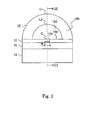
- FIG. 2 is a front view of the electromagnetic wave emission device 1.
- FIG. 3 is a cross sectional view of the electromagnetic wave emission device 1 taken along III-III line (refer to FIG. 2 for III-III line).
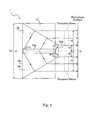
- FIG. 4 is a plan view of the electromagnetic wave emission device 1 (it should be noted that the prism 16 is viewed therethrough). The refraction of the terahertz waves when transmitting through an electromagnetic wave input surface 16a is omitted for the sake of illustration.
- the electromagnetic wave emission device 1 emits electromagnetic waves having a frequency between 0.01 [THz] and 100 [THz].
- the electromagnetic waves emitted from the electromagnetic wave emission device 1 are electromagnetic waves (terahertz waves) within the terahertz waveband (between 0.03 [THz] and 10 [THz]), for example. It is assumed that the electromagnetic waves emitted from the electromagnetic wave emission device 1 are terahertz waves in the following description of embodiments of the present invention.
- the electromagnetic wave emission device 1 includes an excitation light source 2, a nonlinear crystal 10, a buffer layer 12, a substrate 14, and the prism 16.
- the excitation light source 2 outputs an excitation light Lp having two wavelength components (wavelengths ⁇ 1 and ⁇ 2 ).
- the wavelengths ⁇ 1 and ⁇ 2 take values within a range between 1250nm and 1700nm, for example.
- the excitation light Lp is a femtosecond optical pulse, for example.
- the femtosecond optical pulse includes wavelength components other than the two wavelength components (wavelengths ⁇ 1 and ⁇ 2 ), resulting in having two or more wavelength components.
- the nonlinear crystal 10 is an MgO-doped LN crystal, for example.
- the nonlinear crystal 10 has a protruded portion 10a on its surface.
- the protruded portion 10a is an optical waveguide in a ridge shape as shown in FIG. 1 .
- the shape of the optical waveguide is not limited to the ridge shape, a titanium diffused waveguide, a proton-exchanged waveguide, or the like may be provided in the nonlinear crystal 10, instead of the optical waveguide (protruded portion 10a).
- the excitation light Lp is emitted perpendicularly to a side surface (namely, YZ plane) of the nonlinear crystal 10. In other words, the side surface of the nonlinear crystal 10 receives the excitation light Lp.
- the protruded portion 10a is used to prevent extension of a portion through which the excitation light Lp propagates in the width direction of the nonlinear crystal 10 (referring to FIG. 2 , the same direction as the width W of the protruded portion 10a), thereby decreasing the surface area for receiving the excitation light Lp (making the surface area which receives the excitation light Lp be smaller than the entire side surface area of the nonlinear crystal 10), and increasing the power density of the excitation light Lp.
- the width W (refer to FIG. 2 ) of the protruded portion 10a is quite small compared to the wavelength of the terahertz waves and is some ⁇ m to several tens of ⁇ m, for example.
- a polarization plane of the excitation light Lp is parallel to Z axis (axis perpendicular to the paper of FIG. 3 ).
- the two wavelength components of the excitation light Lp form nonlinear polarization near the protruded portion 10a of the nonlinear crystal 10, and electromagnetic waves (terahertz waves) at the frequency corresponding to the polarization are emitted.
- n opt_eff the effective refractive index of the nonlinear crystal 10 at the wavelength of the excitation light Lp
- nTHz the refractive index of the nonlinear crystal 10 at the wavelength of the terahertz wave
- the refractive indices for the two wavelengths ( ⁇ 1 , ⁇ 2 ) contained in the exiting light Lp are different from each other due to the refractive index dispersion of the nonlinear crystal 10.
- the difference of wavelength between ⁇ 1 and ⁇ 2 is quite small with respect to the wavelength of the terahertz waves, and thus the influence of the refractive index dispersion between ⁇ 1 and ⁇ 2 is almost negligible.
- the refractive indices (n 1 , n 2 ) (respectively corresponding to ⁇ 1 , ⁇ 2 ) of the excitation light Lp (wavelengths ⁇ 1 , ⁇ 2 ) in the nonlinear crystal 10 are almost equal to each other and can be considered as n opt_eff .
- the terahertz waves which are spherical waves, are Cherenkov phase-matched and are emitted from the neighborhood of the protruded portion 10a of the nonlinear crystal 10 in the direction at the angle ⁇ satisfying the Cherenkov phase matching represented by the following equation (refer to FIG. 3 ).
- the angle ⁇ is an angle between the travel direction of the excitation light Lp and the travel direction of the terahertz waves referring to FIG. 3 .
- the nonlinear crystal 10 is mounted on the substrate 14. It should be noted that the substrate 14 is, via an adhesive, in contact with an opposite surface to the surface of the nonlinear crystal 10 on which the protruded portion 10a is arranged.
- the substrate 14 is a LN substrate, which is not doped, for example.
- the buffer layer 12 covers the surface of the nonlinear crystal 10 on which the protruded portion 10a is provided and the protruded portion 10a.
- the refractive index of the excitation light Lp (wavelengths ⁇ 1 and ⁇ 2 ) in the buffer layer 12 is smaller than the effective refractive index of the excitation light Lp (wavelengths ⁇ 1 and ⁇ 2 ) in the protruded portion 10a of the nonlinear crystal 10.
- the thickness of the buffer layer 12 is set to be thicker than the penetration length ⁇ of the excitation light Lp, and to be thinner than the wavelength of ⁇ THz of the terahertz waves to be extracted outside the electromagnetic wave emission device 1.
- the refractive index of the excitation light Lp in the prism 16 is larger than the effective refractive index of the excitation light Lp in the nonlinear crystal 10, it is possible to cause the terahertz waves to transmit through the buffer layer 12 while the excitation light Lp is confined in the neighborhood of the protruded portion 10a.
- the prism 16 includes an electromagnetic wave input surface 16a, an electromagnetic wave transmission surface 16b, and bottom surfaces 16c and 16d.
- the electromagnetic wave input surface 16a is in contact with the buffer layer 12, and receives the terahertz waves from the neighborhood of the protruded portion 10a.
- the electromagnetic wave transmission surface 16b is a surface through which the terahertz waves, which have entered from the electromagnetic wave input surface 16a, transmit.
- a material of the prism 16 may thus be high-resistivity silicon or germanium, for example.
- the prism 16 it is preferable for the prism 16 to be transparent in the terahertz waveband and to be free from birefringence.
- the prism 16 has a semicircular truncated cone shape about the central axis C-C on the electromagnetic wave input surface 16a.
- the bottom surface 16c and the bottom surface 16d are two bottom surfaces parallel to each other, and opposed to each other (refer to FIG. 3 ). It should be noted that the shape of the bottom surface 16c is a semicircle (radius thereof is referred to as r1) and the shape of the bottom surface 16d is a semicircle (radius thereof is referred to as r2 ( ⁇ r1)).
- the bottom surface 16c and the bottom surface 16d are orthogonal to the magnetic wave input surface 16a.
- the tilted line segment L and the central axis C-C are on the same plane, and the tilted line segment L is tilted by an angle ⁇ with respect to the central axis C-C.
- the electromagnetic wave transmission surface 16b is a rotation surface which is a trajectory of the tilted line segment L rotated about the central axis C-C.
- the tilted angle ⁇ (refer to FIG. 3 ) to be defined so that the terahertz waves when transmitting through the electromagnetic wave transmission surface 16b are refracted, and travel in parallel to the central axis C-C.
- a description will now be given of how to define the tilted angle ⁇ .
- the terahertz waves are emitted from the neighborhood of the protruded portion 10a and then transmit through the buffer layer 12.
- the angle between the travel direction of the terahertz waves and the travel direction of the excitation light Lp is ⁇ .
- the terahertz waves are refracted when the terahertz waves transmit through the electromagnetic wave input surface 16a of the prism 16, and the angle between the travel direction of the terahertz waves and the travel direction of the excitation light Lp becomes ⁇ CH thereafter.
- ⁇ CH is represented by the following equation.
- n clad is a refractive index of the prism 16 at the wavelength of the terahertz wave. Moreover, the relation n clad >n opt_eff holds true. cos ⁇ CH ⁇ n opt_eff n clad
- FIG. 13 is a diagram showing a relation among an incident angle ⁇ in of the terahertz waves into the electromagnetic wave transmission surface 16b, an emission angle ⁇ out, and the tilted angle ⁇ .
- FIG. 12 is a plan view of the electromagnetic wave emission device 1, and is a diagram showing a positional relation between the central axis C-C and the protruded portion 10a. It should be noted that the prism 16 is viewed therethrough. The central axis C-C and a projection of the optical waveguide (protruded portion 10a) into the electromagnetic wave input surface 16a are shown in FIG. 12 .
- the protruded portion 10a does not reach a plane including the bottom surface 16d and only extends to a position in front of the plane.
- the central axis C-C is parallel to the extension direction of the protruded portion 10a.
- the central axis C-C passes through the projection of the protruded portion 10a into the electromagnetic wave input surface 16a.
- the central axis C-C coincides with the symmetrical axis of the projection of the protruded portion 10a into the electromagnetic wave input surface 16a.
- the exiting light Lp is fed to the nonlinear crystal 10 from the excitation light source 2.
- the excitation light Lp travels approximately straight in the neighborhood of the protruded portion 10a.
- the two wavelength components (wavelengths ⁇ 1 and ⁇ 2 ) of the excitation light Lp form the nonlinear polarization in the neighborhood of the protruded portion 10a of the nonlinear crystal 10, and the terahertz waves at the frequency corresponding to the polarization are emitted.
- the travel direction of the terahertz waves emitted from the neighborhood of the protruded portion 10a of the nonlinear crystal 10 satisfying the condition n THz > n opt_eff forms the angle ⁇ satisfying the Cherenkov phase matching with respect to the travel direction of the excitation light Lp (refer to FIG. 3 ).
- the terahertz waves emitted from the neighborhood of the protruded portion 10a transmit through the buffer layer 12.
- the angle between the travel direction of the terahertz waves and the travel direction of the excitation light Lp at this time is ⁇ .
- the terahertz waves are refracted when the terahertz waves transmit through the electromagnetic wave input surface 16a of the prism 16, and the angle between the travel direction of the terahertz waves and the travel direction of the excitation light Lp forms ⁇ CH thereafter.
- the terahertz waves which have traveled inside the prism 16 are refracted when transmitting through the electromagnetic wave transmission surface 16b, and travel in parallel to the central axis C-C.
- An equiphase surface parallel to the bottom surface 16c and the bottom surface 16d are irradiated with the terahertz waves which have traveled in parallel to the central axis C-C, for example.
- an area within the distance between r2 and r3 from the central axis on the equiphase surface is irradiated with the terahertz waves which have transmitted through the tilted line segment L.
- the area within the distance between r2 and r3 from the central axis on the equiphase surface is also irradiated with the terahertz waves which have transmitted through a line where the electromagnetic wave input surface 16a and the electromagnetic wave transmission surface 16b intersect with each other.
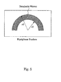
- FIG. 5 is a diagram showing the area irradiated with the terahertz waves on the equiphase surface. It should be noted that the area irradiated with the terahertz waves are hatched in FIG. 5 .
- the area irradiated with the terahertz waves has an approximately semicircular shape having an inner diameter r2 and an outer diameter r3.
- a case (comparative example) in which a triangular prism 116 (refer to FIG. 5 of Patent Document 1, for example) is used instead of the prism 16 is compared to this embodiment.
- the comparative example corresponds to such a configuration that an optical waveguide in a ridge shape is provided in a nonlinear optical crystal according to Patent Document 1.
- FIG. 6 is a side cross sectional view of the electromagnetic wave emission device 1 according to the comparative example.
- FIG. 7 is a front view of the electromagnetic wave emission device 1 according to the comparative example.
- FIG. 8 is a cross sectional view of the electromagnetic emission device 1 according to the comparative example taken along P-P line (refer to FIG. 6 for P-P).
- the P-P plane is a plane parallel to a side surface of the nonlinear crystal 10 (namely YZ surface) in the buffer layer 12, the protruded portion 10a, the nonlinear crystal 10, and the substrate 14, and tilted with respect to a YZ plane by (90° - ⁇ ch ) in the triangular prism 116.
- the triangular prism 116 includes an electromagnetic wave input surface 116a (same as the electromagnetic wave input surface 16a) and an electromagnetic wave transmission surface 116b.
- the electromagnetic wave transmission surface 116b is tilted with respective to the electromagnetic wave input surface 116a. It should be noted that a direction of a normal line of the electromagnetic wave transmission surface 116b coincides with the travel direction of the terahertz waves.
- An angle formed by the travel direction of the terahertz waves traveling in the triangular prism 116 and the travel direction of the excitation light Lp is ⁇ CH both for the comparative example and this embodiment.
- the terahertz waves are not refracted and travel straight when transmitting through the electromagnetic wave transmission surface 16b in FIG. 6 . However, this occurs in the case where the terahertz waves travel toward a position immediately above the protruded portion 10a as shown in FIG. 8 .
- the terahertz waves are diffracted in the direction of the width W of the protruded portion 10a in the comparative example.
- the travel direction of the terahertz waves is displaced from the position immediately above the protruded portion 10a even by a slight angle, the terahertz waves are fully reflected by the electromagnetic wave transmission surface 116b.
- the output of the terahertz waves emitted by the electromagnetic wave emission device 1 is decreased.
- the slight angle is 17.1°, for example.
- the refractive index of the terahertz wave in the triangular prism 116 is 3.4
- the refractive index of the terahertz wave in the air is 1.
- the terahertz waves generated in the neighborhood of the protruded portion 10a are fully reflected at the interface between the protruded portion 10a and the air, and cannot be extracted outside the protruded portion 10a.
- the triangular prism 116 is arranged on the protruded portion 10a as in the comparative example, the terahertz waves which travel immediately above the protruded portion 10a can be extracted outside the protruded portion 10a.
- the travel direction of the terahertz waves is displaced from the position immediately above the protruded portion 10a even by a slight angle, the terahertz waves are fully reflected by the electromagnetic wave transmission surface 116b.
- the prism 16 is arranged on the protruded portion 10a, and the electromagnetic wave transmission surface 16b of the prism 16 is configured to be the rotation surface obtained by rotating the tilted line segment L about the central axis C-C by 180°, and as a result, even if the travel direction of the terahertz wave is displaced from the position immediate above the protruded portion 10a, the terahertz wave transmits through the electromagnetic wave transmission surface 16b. As a result, the output power of the terahertz waves of the electromagnetic wave emission device 1 can be increased.
- the tilted angle ⁇ of the tilted line segment L is defined so that the terahertz waves are refracted when transmitting through the electromagnetic wave transmission surface 16b and travel in parallel to the central axis C-C, so that the collimated terahertz waves be extracted.
- the prism 16 has been described as semicircular truncated cone, the shape of the prism 16 is not necessarily limited to the semicircular truncated cone.
- both ends L1 and L2 of the tilted line segment L may be on the lines of travel of the terahertz waves traveling in the prism 16 from both ends C1 and C2 of a portion of the central axis C-C which receives the terahertz waves out.
- a description will now be given of a variation in which the tilted line segment L is set as described above.
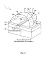
- FIG. 9 is a perspective view of the electromagnetic wave emission device 1 according to a first variation example of the present invention.
- FIG. 10 is a side cross sectional view of the electromagnetic wave emission device 1 according to the first variation example of the present invention.
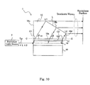
- the prism 16 is a combination of a semicircular truncated cone and a semi-cylinder, in the first variation example of the present invention.
- the end L1 of the tilted line segment L closer to the excitation light source 2 is on the line of travel of the terahertz wave traveling inside the prism 16 from the end C1 closer to the excitation light source 2 of the portion of the central axis C-C which receives the terahertz waves.
- the variation is different at this point from the above-described embodiment of the present invention (refer to FIG. 3 ) in which the end L1 of the tilted line segment L closer to the excitation light source 2 is immediately above C.
- the end L2 of the tilted line segment L farther from the excitation light source 2 is on the line of travel of the terahertz wave traveling inside the prism 16 from the end C2 farther from the excitation light source 2 of the portion of the central axis C-C which receives the terahertz waves.
- This point is the same as the above-described embodiment (refer to FIG. 3 ) of the present invention.
- the electromagnetic wave transmission surface 16 includes the rotation surface (curved surface of a semicircular truncated cone) which is a trajectory of the tilted line segment L rotated about the central axis C-C, and a curved surface (curved surface of a semi-cylinder) which is a trajectory obtained by rotating, about the central axis C-C, a line which passes through the end L1 and is parallel to the central axis C-C.
- the same effects as in the above-described embodiment of the present invention can be obtained also by the first variation example of the present invention.
- the shape of the electromagnetic wave transmission surface 16 closer to the excitation light source 2 than the end L1 is not necessarily limited to the curved surface of a semi-cylinder, but is arbitrary in the first variation example of the present invention.
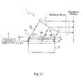
- FIG. 11 is a side cross sectional view of the electromagnetic wave emission device 1 according to a second variation example of the present invention.
- the both ends L1 and L2 of the tilted line segment L are the same as those in the first variation example.
- the side cross section of the second variation example of the electromagnetic wave emission device 1 has a trapezoidal shape formed by a line C1L1, a line L1L2, a line L2C2, and a line C2C1. By rotating the trapezoid about the central axis C-C by 180°, the electromagnetic emission device 1 according to the second variation example is obtained.
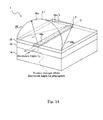
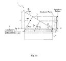
- the prism 16 may be half-cone, which is considered as a third variation example of the present invention.
- FIG. 14 is a perspective view of the electromagnetic wave emission device 1 according to the third variation example of the present invention.
- FIG. 15 is a side cross sectional view of the electromagnetic wave emission device 1 according to the third variation example of the present invention.
- FIG. 16 is a plan view of the electromagnetic wave emission device 1 according to the third variation example of the present invention and is a diagram showing a positional relation between the central axis C-C and the protruded portion 10a. It should be noted that the prism 16 is viewed therethrough in FIG. 16 . The central axis C-C and a projection of the optical waveguide (protruded portion 10a) into the electromagnetic wave input surface 16a are shown in FIG. 16 . The positional relation between the central axis C-C and the protruded portion 10a are the same as that in the embodiment.
- FIG. 17 is a diagram showing an area irradiated with the terahertz waves on the equiphase surface in the electromagnetic wave emission device 1 according to the third variation example of the present invention.
Landscapes
- Physics & Mathematics (AREA)
- Nonlinear Science (AREA)
- General Physics & Mathematics (AREA)
- Optics & Photonics (AREA)
- Engineering & Computer Science (AREA)
- General Engineering & Computer Science (AREA)
- Spectroscopy & Molecular Physics (AREA)
- Optical Modulation, Optical Deflection, Nonlinear Optics, Optical Demodulation, Optical Logic Elements (AREA)
Abstract
Description
- The present invention relates to an emission of electromagnetic waves (frequency thereof is between 0.01 [THz] and 100 [THz]) (such as terahertz waves (frequency thereof is between 0.03 [THz] and 10 [THz])), for example).
- A broadband terahertz wave generation method by means of a difference frequency terahertz wave generation using the Cerenkov radiation has been proposed (refer to
Fig. 2 ofNon-Patent Document 1 andFIG. 1 of Patent Document 1). Excitation light from a light source (KTP-OPO excited by Nd-YAG laser, for example) outputting two wavelengths is emitted to a nonlinear crystal (MgO-doped LN crystal, for example) according toFig. 2 ofNon-Patent Document 1. The incident excitation light having the two wavelengths induces nonlinear polarization in the MgO-doped LN crystal. If the MgO-doped LN crystal satisfies the condition (nTHz>nopt) of the Cerenkov radiation, a spherical wave which takes the maximal value at each position corresponding to the twice of the coherence length is generated. This spherical wave has a wave front aligned in the direction of radiation angle θ satisfying the following relation, and the terahertz waves are emitted in this direction. It should be noted that nopt denotes a refractive index in the excitation light waveband of the MgO-doped LN crystal, and nTHz is a refractive index in the terahertz waveband of the MgO-doped LN crystal.
[Non-Patent Document 1] K. Suizu, K. Koketsu, T. Shibuya, T. Tsutsui, T. Akiba, and K. Kawase, "Extremely frequency-widened terahertz wave generation using Cherenkov-type radiation," Opt. Express 17(8), pages 6676-6681, 2009
[Patent Document 1]JP 2010-204488 A - An object of the present invention is to increase the output power of the terahertz waves.
- According to the present invention, an electromagnetic wave emission device includes: a nonlinear crystal that receives excitation light having at least two wave length components, outputs an electromagnetic wave having a frequency between 0.01 [THz] and 100 [THz] through the Cherenkov phase matching, the nonlinear crystal having an optical waveguide; and a prism that includes an electromagnetic wave input surface which receives the electromagnetic wave from the optical waveguide and an electromagnetic wave transmission surface through which the electromagnetic wave that has entered the electromagnetic wave input surface transmits, wherein: the electromagnetic wave transmission surface includes a rotation surface which is a trajectory of a tilted line segment rotated about a central axis of the electromagnetic wave input surface, the tilted line segment being tilted with respect to the central axis; the tilted line segment and the central axis are on the same plane; the central axis is in parallel to an extending direction of the optical waveguide; and the central axis passes through a projection of the optical waveguide into the electromagnetic wave input surface.
- According to the thus constructed electromagnetic wave emission device, a nonlinear crystal receives excitation light having at least two wave length components, outputs an electromagnetic wave having a frequency between 0.01 [THz] and 100 [THz] through the Cherenkov phase matching, the nonlinear crystal having an optical waveguide. A prism includes an electromagnetic wave input surface which receives the electromagnetic wave from the optical waveguide and an electromagnetic wave transmission surface through which the electromagnetic wave that has entered the electromagnetic wave input surface transmits. The electromagnetic wave transmission surface includes a rotation surface which is a trajectory of a tilted line segment rotated about a central axis of the electromagnetic wave input surface, the tilted line segment being tilted with respect to the central axis. The tilted line segment and the central axis are on the same plane. The central axis is in parallel to an extending direction of the optical waveguide. The central axis passes through a projection of the optical waveguide into the electromagnetic wave input surface.
- According to the electromagnetic wave emission device of the present invention, a tilted angle of the tilted line segment with respect to the central axis may be determined so that the electromagnetic wave is refracted when transmitting through the electromagnetic wave transmission surface and travels in parallel to the central axis.
- According to the electromagnetic wave emission device of the present invention, the rotation surface may be a trajectory of the tilted line segment rotated by 180 degrees about the central axis.
- According to the electromagnetic wave emission device of the present invention, both ends of the tilted line segment may be on the line of travel of the electromagnetic wave traveling inside the prism from both ends of a portion of the central axis which receives the electromagnetic wave.
- According to the electromagnetic wave emission device of the present invention, the optical waveguide may be a portion protruding from the nonlinear crystal.
- According to the present invention, the electromagnetic wave emission device may include a buffer layer arranged between the prism and the nonlinear crystal, wherein the buffer layer is thicker than a penetration length of the excitation light and is thinner than the wavelength of the electromagnetic wave.
-
-
FIG. 1 is a perspective view of an electromagneticwave emission device 1 according to an embodiment of the present invention; -
FIG. 2 is a front view of the electromagneticwave emission device 1; -
FIG. 3 is a cross sectional view of the electromagneticwave emission device 1 taken along III-III line (refer toFIG. 2 for III-III line); -
FIG. 4 is a plan view of the electromagnetic wave emission device 1 (it should be noted that theprism 16 is viewed therethrough); -
FIG. 5 is a diagram showing the area irradiated with the terahertz waves on the equiphase surface; -
FIG. 6 is a side cross sectional view of the electromagneticwave emission device 1 according to the comparative example; -
FIG. 7 is a front view of the electromagneticwave emission device 1 according to the comparative example; -
FIG. 8 is a cross sectional view of theelectromagnetic emission device 1 according to the comparative example taken along P-P line (refer toFIG. 6 for P-P); -
FIG. 9 is a perspective view of the electromagneticwave emission device 1 according to a first variation example of the present invention; -
FIG. 10 is a side cross sectional view of the electromagneticwave emission device 1 according to the first variation example of the present invention; -
FIG. 11 is a side cross sectional view of the electromagneticwave emission device 1 according to a second variation example of the present invention; -
FIG. 12 is a plan view of the electromagneticwave emission device 1, and is a diagram showing a positional relation between the central axis C-C and theprotruded portion 10a; -
FIG. 13 is a diagram showing a relation among an incident angle θ in of the terahertz waves into the electromagneticwave transmission surface 16b, an emission angle θ out, and the tilted angle α; -
FIG. 14 is a perspective view of the electromagneticwave emission device 1 according to the third variation example of the present invention; -
FIG. 15 is a side cross sectional view of the electromagneticwave emission device 1 according to the third variation example of the present invention; -
FIG. 16 is a plan view of the electromagneticwave emission device 1 according to the third variation example of the present invention and is a diagram showing a positional relation between the central axis C-C and theprotruded portion 10a; and -
FIG. 17 is a diagram showing an area irradiated with the terahertz waves on the equiphase surface in the electromagneticwave emission device 1 according to the third variation example of the present invention. - A description will now be given of an embodiment of the present invention referring to drawings.
-
FIG. 1 is a perspective view of an electromagneticwave emission device 1 according to an embodiment of the present invention.FIG. 2 is a front view of the electromagneticwave emission device 1.FIG. 3 is a cross sectional view of the electromagneticwave emission device 1 taken along III-III line (refer toFIG. 2 for III-III line).FIG. 4 is a plan view of the electromagnetic wave emission device 1 (it should be noted that theprism 16 is viewed therethrough). The refraction of the terahertz waves when transmitting through an electromagneticwave input surface 16a is omitted for the sake of illustration. - The electromagnetic
wave emission device 1 emits electromagnetic waves having a frequency between 0.01 [THz] and 100 [THz]. The electromagnetic waves emitted from the electromagneticwave emission device 1 are electromagnetic waves (terahertz waves) within the terahertz waveband (between 0.03 [THz] and 10 [THz]), for example. It is assumed that the electromagnetic waves emitted from the electromagneticwave emission device 1 are terahertz waves in the following description of embodiments of the present invention. - The electromagnetic
wave emission device 1 includes anexcitation light source 2, anonlinear crystal 10, abuffer layer 12, asubstrate 14, and theprism 16. - Referring to
FIG. 3 , theexcitation light source 2 outputs an excitation light Lp having two wavelength components (wavelengths λ 1 and λ 2). The wavelengths λ 1 and λ 2 take values within a range between 1250nm and 1700nm, for example. The excitation light Lp is a femtosecond optical pulse, for example. The femtosecond optical pulse includes wavelength components other than the two wavelength components (wavelengths λ 1 and λ 2), resulting in having two or more wavelength components. - The
nonlinear crystal 10 is an MgO-doped LN crystal, for example. Thenonlinear crystal 10 has a protrudedportion 10a on its surface. Theprotruded portion 10a is an optical waveguide in a ridge shape as shown inFIG. 1 . However, the shape of the optical waveguide is not limited to the ridge shape, a titanium diffused waveguide, a proton-exchanged waveguide, or the like may be provided in thenonlinear crystal 10, instead of the optical waveguide (protrudedportion 10a). The excitation light Lp is emitted perpendicularly to a side surface (namely, YZ plane) of thenonlinear crystal 10. In other words, the side surface of thenonlinear crystal 10 receives the excitation light Lp. It is necessary to increase the power density of the excitation light Lp in order to realize a high output of the terahertz waves emitted by the electromagneticwave emission device 1. Then, the protrudedportion 10a is used to prevent extension of a portion through which the excitation light Lp propagates in the width direction of the nonlinear crystal 10 (referring toFIG. 2 , the same direction as the width W of the protrudedportion 10a), thereby decreasing the surface area for receiving the excitation light Lp (making the surface area which receives the excitation light Lp be smaller than the entire side surface area of the nonlinear crystal 10), and increasing the power density of the excitation light Lp. The width W (refer toFIG. 2 ) of the protrudedportion 10a is quite small compared to the wavelength of the terahertz waves and is some µ m to several tens of µ m, for example. - It should be noted that a polarization plane of the excitation light Lp is parallel to Z axis (axis perpendicular to the paper of
FIG. 3 ). The two wavelength components of the excitation light Lp form nonlinear polarization near the protrudedportion 10a of thenonlinear crystal 10, and electromagnetic waves (terahertz waves) at the frequency corresponding to the polarization are emitted. It should be noted that if the effective refractive index of thenonlinear crystal 10 at the wavelength of the excitation light Lp is denoted by nopt_eff, and the refractive index of thenonlinear crystal 10 at the wavelength of the terahertz wave is nTHz, a relation nTHz>nopt_eff holds true. The refractive indices for the two wavelengths (λ 1, λ 2) contained in the exiting light Lp are different from each other due to the refractive index dispersion of thenonlinear crystal 10. However, the difference of wavelength between λ 1 and λ 2 is quite small with respect to the wavelength of the terahertz waves, and thus the influence of the refractive index dispersion between λ 1 and λ 2 is almost negligible. Thus, the refractive indices (n1, n2) (respectively corresponding to λ 1, λ 2) of the excitation light Lp (wavelengths λ 1, λ 2) in thenonlinear crystal 10 are almost equal to each other and can be considered as nopt_eff. - If an angle satisfying the Cerenkov phase matching is θ, the relation cos θ =(λ THz/nTHz)/(λ 1 λ 2/(n1 λ 2 - n2 λ 1)) holds true. Here, the wavelength of the terahertz waves is λ THz.
- The terahertz waves, which are spherical waves, are Cherenkov phase-matched and are emitted from the neighborhood of the protruded
portion 10a of thenonlinear crystal 10 in the direction at the angle θ satisfying the Cherenkov phase matching represented by the following equation (refer toFIG. 3 ). It should be noted that the angle θ is an angle between the travel direction of the excitation light Lp and the travel direction of the terahertz waves referring toFIG. 3 . The following is an equation if it is assumed that n1=n2=nopt_eff in cos θ =(λ THz/nTHz)(λ 1 λ 2/(n1 λ 2 - n2 λ 1)).
- The
nonlinear crystal 10 is mounted on thesubstrate 14. It should be noted that thesubstrate 14 is, via an adhesive, in contact with an opposite surface to the surface of thenonlinear crystal 10 on which the protrudedportion 10a is arranged. Thesubstrate 14 is a LN substrate, which is not doped, for example. - The
buffer layer 12 covers the surface of thenonlinear crystal 10 on which the protrudedportion 10a is provided and the protrudedportion 10a. The refractive index of the excitation light Lp (wavelengths λ 1 and λ 2) in thebuffer layer 12 is smaller than the effective refractive index of the excitation light Lp (wavelengths λ 1 and λ 2) in the protrudedportion 10a of thenonlinear crystal 10. Moreover, the thickness of thebuffer layer 12 is set to be thicker than the penetration length ξ of the excitation light Lp, and to be thinner than the wavelength of λ THz of the terahertz waves to be extracted outside the electromagneticwave emission device 1. As a result, even if the refractive index of the excitation light Lp in theprism 16 is larger than the effective refractive index of the excitation light Lp in thenonlinear crystal 10, it is possible to cause the terahertz waves to transmit through thebuffer layer 12 while the excitation light Lp is confined in the neighborhood of the protrudedportion 10a. - The
prism 16 includes an electromagneticwave input surface 16a, an electromagneticwave transmission surface 16b, andbottom surfaces wave input surface 16a is in contact with thebuffer layer 12, and receives the terahertz waves from the neighborhood of the protrudedportion 10a. The electromagneticwave transmission surface 16b is a surface through which the terahertz waves, which have entered from the electromagneticwave input surface 16a, transmit. - It is preferable for absorption of the terahertz waves to be small, in order to reduce a transmission loss of the terahertz waves in the
prism 16. A material of theprism 16 may thus be high-resistivity silicon or germanium, for example. Moreover, it is preferable for theprism 16 to be transparent in the terahertz waveband and to be free from birefringence. - The
prism 16 has a semicircular truncated cone shape about the central axis C-C on the electromagneticwave input surface 16a. Thebottom surface 16c and thebottom surface 16d are two bottom surfaces parallel to each other, and opposed to each other (refer toFIG. 3 ). It should be noted that the shape of thebottom surface 16c is a semicircle (radius thereof is referred to as r1) and the shape of thebottom surface 16d is a semicircle (radius thereof is referred to as r2 (<r1)). Thebottom surface 16c and thebottom surface 16d are orthogonal to the magneticwave input surface 16a. - Referring to
FIG. 3 , the tilted line segment L and the central axis C-C are on the same plane, and the tilted line segment L is tilted by an angle α with respect to the central axis C-C. The electromagneticwave transmission surface 16b is a rotation surface which is a trajectory of the tilted line segment L rotated about the central axis C-C. - It should be noted that the electromagnetic
wave transmission surface 16b can be considered as a rotation surface obtained by rotating the tilted line segment L about the central axis C-C by 90° counterclockwise and further rotating clockwise by 90° clockwise (namely, rotating the tilted line segment L about the central axis C-C by 180° (=90°+90°)) viewed from thebottom surface 16c. - It should be noted that it is preferable for the tilted angle α (refer to
FIG. 3 ) to be defined so that the terahertz waves when transmitting through the electromagneticwave transmission surface 16b are refracted, and travel in parallel to the central axis C-C. A description will now be given of how to define the tilted angle α. - Referring to
FIG. 3 , the terahertz waves are emitted from the neighborhood of the protrudedportion 10a and then transmit through thebuffer layer 12. On this occasion, the angle between the travel direction of the terahertz waves and the travel direction of the excitation light Lp is θ. After the transmission through thebuffer layer 12, the terahertz waves are refracted when the terahertz waves transmit through the electromagneticwave input surface 16a of theprism 16, and the angle between the travel direction of the terahertz waves and the travel direction of the excitation light Lp becomes θ CH thereafter. It should be noted that θ CH is represented by the following equation. It should also be noted that nclad is a refractive index of theprism 16 at the wavelength of the terahertz wave. Moreover, the relation nclad>nopt_eff holds true.
- For example, if nopt_eff=2.173 and nclad=3.415, then θ CH=50.5°.
-
FIG. 13 is a diagram showing a relation among an incident angle θ in of the terahertz waves into the electromagneticwave transmission surface 16b, an emission angle θ out, and the tilted angle α. Referring toFIG. 13 , the following relations hold true for the incident angle θ in, the emission angle θ out, and the tilted angle α.

- Moreover, according to the Snell's law, a relation:

holds true (here, it is assumed that the refractive index of the air around the electromagneticwave emission device 1 is 1). - For example, α =24° is obtained by assigning θ CH=50.5° and nclad=3.415 to the equation described above.
-
FIG. 12 is a plan view of the electromagneticwave emission device 1, and is a diagram showing a positional relation between the central axis C-C and the protrudedportion 10a. It should be noted that theprism 16 is viewed therethrough. The central axis C-C and a projection of the optical waveguide (protrudedportion 10a) into the electromagneticwave input surface 16a are shown inFIG. 12 . - The protruded
portion 10a does not reach a plane including thebottom surface 16d and only extends to a position in front of the plane. The central axis C-C is parallel to the extension direction of the protrudedportion 10a. The central axis C-C passes through the projection of the protrudedportion 10a into the electromagneticwave input surface 16a. For example, the central axis C-C coincides with the symmetrical axis of the projection of the protrudedportion 10a into the electromagneticwave input surface 16a. - A description will now be given of an operation according to embodiments of the present invention.
- The exiting light Lp is fed to the
nonlinear crystal 10 from theexcitation light source 2. The excitation light Lp travels approximately straight in the neighborhood of the protrudedportion 10a. The two wavelength components (wavelengths λ 1 and λ 2) of the excitation light Lp form the nonlinear polarization in the neighborhood of the protrudedportion 10a of thenonlinear crystal 10, and the terahertz waves at the frequency corresponding to the polarization are emitted. Moreover, the travel direction of the terahertz waves emitted from the neighborhood of the protrudedportion 10a of thenonlinear crystal 10 satisfying the condition nTHz > nopt_eff forms the angle θ satisfying the Cherenkov phase matching with respect to the travel direction of the excitation light Lp (refer toFIG. 3 ). - The terahertz waves emitted from the neighborhood of the protruded
portion 10a transmit through thebuffer layer 12. The angle between the travel direction of the terahertz waves and the travel direction of the excitation light Lp at this time is θ. After the transmission through thebuffer layer 12, the terahertz waves are refracted when the terahertz waves transmit through the electromagneticwave input surface 16a of theprism 16, and the angle between the travel direction of the terahertz waves and the travel direction of the excitation light Lp forms θ CH thereafter. - The terahertz waves which have traveled inside the
prism 16 are refracted when transmitting through the electromagneticwave transmission surface 16b, and travel in parallel to the central axis C-C. An equiphase surface parallel to thebottom surface 16c and thebottom surface 16d are irradiated with the terahertz waves which have traveled in parallel to the central axis C-C, for example. - Referring to
FIG. 3 , an area within the distance between r2 and r3 from the central axis on the equiphase surface is irradiated with the terahertz waves which have transmitted through the tilted line segment L. Moreover, referring toFIG. 4 , the area within the distance between r2 and r3 from the central axis on the equiphase surface is also irradiated with the terahertz waves which have transmitted through a line where the electromagneticwave input surface 16a and the electromagneticwave transmission surface 16b intersect with each other. -
FIG. 5 is a diagram showing the area irradiated with the terahertz waves on the equiphase surface. It should be noted that the area irradiated with the terahertz waves are hatched inFIG. 5 . The area irradiated with the terahertz waves has an approximately semicircular shape having an inner diameter r2 and an outer diameter r3. - On this occasion, a case (comparative example) in which a triangular prism 116 (refer to
FIG. 5 ofPatent Document 1, for example) is used instead of theprism 16 is compared to this embodiment. The comparative example corresponds to such a configuration that an optical waveguide in a ridge shape is provided in a nonlinear optical crystal according toPatent Document 1. -
FIG. 6 is a side cross sectional view of the electromagneticwave emission device 1 according to the comparative example.FIG. 7 is a front view of the electromagneticwave emission device 1 according to the comparative example.FIG. 8 is a cross sectional view of theelectromagnetic emission device 1 according to the comparative example taken along P-P line (refer toFIG. 6 for P-P). - It should be noted that the P-P plane is a plane parallel to a side surface of the nonlinear crystal 10 (namely YZ surface) in the
buffer layer 12, the protrudedportion 10a, thenonlinear crystal 10, and thesubstrate 14, and tilted with respect to a YZ plane by (90° - θ ch) in thetriangular prism 116. - The
triangular prism 116 includes an electromagneticwave input surface 116a (same as the electromagneticwave input surface 16a) and an electromagneticwave transmission surface 116b. The electromagneticwave transmission surface 116b is tilted with respective to the electromagneticwave input surface 116a. It should be noted that a direction of a normal line of the electromagneticwave transmission surface 116b coincides with the travel direction of the terahertz waves. - An angle formed by the travel direction of the terahertz waves traveling in the
triangular prism 116 and the travel direction of the excitation light Lp is θ CH both for the comparative example and this embodiment. - The terahertz waves are not refracted and travel straight when transmitting through the electromagnetic
wave transmission surface 16b inFIG. 6 . However, this occurs in the case where the terahertz waves travel toward a position immediately above the protrudedportion 10a as shown inFIG. 8 . - Referring to
FIG. 8 , the terahertz waves are diffracted in the direction of the width W of the protrudedportion 10a in the comparative example. Thus, if the travel direction of the terahertz waves is displaced from the position immediately above the protrudedportion 10a even by a slight angle, the terahertz waves are fully reflected by the electromagneticwave transmission surface 116b. As a result, the output of the terahertz waves emitted by the electromagneticwave emission device 1 is decreased. It should be noted that the slight angle is 17.1°, for example. Here, the refractive index of the terahertz wave in thetriangular prism 116 is 3.4, and the refractive index of the terahertz wave in the air is 1. - According to embodiments of the present invention, the following effects can be obtained.
- If nothing is arranged on the protruded
portion 10a, the terahertz waves generated in the neighborhood of the protrudedportion 10a are fully reflected at the interface between the protrudedportion 10a and the air, and cannot be extracted outside the protrudedportion 10a. Moreover, if thetriangular prism 116 is arranged on the protrudedportion 10a as in the comparative example, the terahertz waves which travel immediately above the protrudedportion 10a can be extracted outside the protrudedportion 10a. However, if the travel direction of the terahertz waves is displaced from the position immediately above the protrudedportion 10a even by a slight angle, the terahertz waves are fully reflected by the electromagneticwave transmission surface 116b. - Therefore, in the embodiments of the present invention, the
prism 16 is arranged on the protrudedportion 10a, and the electromagneticwave transmission surface 16b of theprism 16 is configured to be the rotation surface obtained by rotating the tilted line segment L about the central axis C-C by 180°, and as a result, even if the travel direction of the terahertz wave is displaced from the position immediate above the protrudedportion 10a, the terahertz wave transmits through the electromagneticwave transmission surface 16b. As a result, the output power of the terahertz waves of the electromagneticwave emission device 1 can be increased. - Moreover, the tilted angle α of the tilted line segment L is defined so that the terahertz waves are refracted when transmitting through the electromagnetic
wave transmission surface 16b and travel in parallel to the central axis C-C, so that the collimated terahertz waves be extracted. - Although the
prism 16 has been described as semicircular truncated cone, the shape of theprism 16 is not necessarily limited to the semicircular truncated cone. - For example, both ends L1 and L2 of the tilted line segment L may be on the lines of travel of the terahertz waves traveling in the
prism 16 from both ends C1 and C2 of a portion of the central axis C-C which receives the terahertz waves out. A description will now be given of a variation in which the tilted line segment L is set as described above. -
FIG. 9 is a perspective view of the electromagneticwave emission device 1 according to a first variation example of the present invention.FIG. 10 is a side cross sectional view of the electromagneticwave emission device 1 according to the first variation example of the present invention. - The
prism 16 is a combination of a semicircular truncated cone and a semi-cylinder, in the first variation example of the present invention. Referring toFIG. 10 , the end L1 of the tilted line segment L closer to theexcitation light source 2 is on the line of travel of the terahertz wave traveling inside theprism 16 from the end C1 closer to theexcitation light source 2 of the portion of the central axis C-C which receives the terahertz waves. The variation is different at this point from the above-described embodiment of the present invention (refer toFIG. 3 ) in which the end L1 of the tilted line segment L closer to theexcitation light source 2 is immediately above C. - Referring to
FIG. 10 , the end L2 of the tilted line segment L farther from theexcitation light source 2 is on the line of travel of the terahertz wave traveling inside theprism 16 from the end C2 farther from theexcitation light source 2 of the portion of the central axis C-C which receives the terahertz waves. This point is the same as the above-described embodiment (refer toFIG. 3 ) of the present invention. - The electromagnetic
wave transmission surface 16 includes the rotation surface (curved surface of a semicircular truncated cone) which is a trajectory of the tilted line segment L rotated about the central axis C-C, and a curved surface (curved surface of a semi-cylinder) which is a trajectory obtained by rotating, about the central axis C-C, a line which passes through the end L1 and is parallel to the central axis C-C. - The same effects as in the above-described embodiment of the present invention can be obtained also by the first variation example of the present invention. The shape of the electromagnetic
wave transmission surface 16 closer to theexcitation light source 2 than the end L1 is not necessarily limited to the curved surface of a semi-cylinder, but is arbitrary in the first variation example of the present invention. -
FIG. 11 is a side cross sectional view of the electromagneticwave emission device 1 according to a second variation example of the present invention. The both ends L1 and L2 of the tilted line segment L are the same as those in the first variation example. However, the side cross section of the second variation example of the electromagneticwave emission device 1 has a trapezoidal shape formed by a line C1L1, a line L1L2, a line L2C2, and a line C2C1. By rotating the trapezoid about the central axis C-C by 180°, theelectromagnetic emission device 1 according to the second variation example is obtained. - The same effects as in the above-described embodiment of the present invention can be obtained also by the second variation example embodiment.
- For example, the
prism 16 may be half-cone, which is considered as a third variation example of the present invention. -
FIG. 14 is a perspective view of the electromagneticwave emission device 1 according to the third variation example of the present invention.FIG. 15 is a side cross sectional view of the electromagneticwave emission device 1 according to the third variation example of the present invention. - The electromagnetic
wave emission device 1 according to the third variation example corresponds to a configuration in which the tilted angle is kept α =24° as in the above-described embodiment and r2=0. -
FIG. 16 is a plan view of the electromagneticwave emission device 1 according to the third variation example of the present invention and is a diagram showing a positional relation between the central axis C-C and the protrudedportion 10a. It should be noted that theprism 16 is viewed therethrough inFIG. 16 . The central axis C-C and a projection of the optical waveguide (protrudedportion 10a) into the electromagneticwave input surface 16a are shown inFIG. 16 . The positional relation between the central axis C-C and the protrudedportion 10a are the same as that in the embodiment. -
FIG. 17 is a diagram showing an area irradiated with the terahertz waves on the equiphase surface in the electromagneticwave emission device 1 according to the third variation example of the present invention. The area irradiated with the terahertz waves according to the third variation example corresponds to a semicircle (with a radius r3) obtained when r2=0 in the area shown inFIG. 5 .
Claims (6)
- An electromagnetic wave emission device comprising:a nonlinear crystal that receives excitation light having at least two wave length components, outputs an electromagnetic wave having a frequency between 0.01 [THz] and 100 [THz] through the Cherenkov phase matching, the nonlinear crystal having an optical waveguide; anda prism that includes an electromagnetic wave input surface which receives the electromagnetic wave from the optical waveguide and an electromagnetic wave transmission surface through which the electromagnetic wave that has entered the electromagnetic wave input surface transmits, wherein:the electromagnetic wave transmission surface includes a rotation surface which is a trajectory of a tilted line segment rotated about a central axis of the electromagnetic wave input surface, the tilted line segment being tilted with respect to the central axis;the tilted line segment and the central axis are on the same plane;the central axis is in parallel to an extending direction of the optical waveguide; andthe central axis passes through a projection of the optical waveguide into the electromagnetic wave input surface.
- The electromagnetic wave emission device according to claim 1, wherein a tilted angle of the tilted line segment with respect to the central axis is determined so that the electromagnetic wave is refracted when transmitting through the electromagnetic wave transmission surface and travels in parallel to the central axis.
- The electromagnetic wave emission device according to claim 1, wherein the rotation surface is a trajectory of the tilted line segment rotated by 180 degrees about the central axis.
- The electromagnetic wave emission device according to claim 1, wherein both ends of the tilted line segment are on the line of travel of the electromagnetic wave traveling inside the prism from both ends of a portion of the central axis which receives the electromagnetic wave.
- The electromagnetic wave emission device according to claim 1, wherein the optical waveguide is a portion protruding from the nonlinear crystal.
- The electromagnetic wave emission device according to claim 1, comprising a buffer layer arranged between the prism and the nonlinear crystal, wherein the buffer layer is thicker than a penetration length of the excitation light and is thinner than the wavelength of the electromagnetic wave.
Applications Claiming Priority (1)
| Application Number | Priority Date | Filing Date | Title |
|---|---|---|---|
| JP2012102797A JP5973774B2 (en) | 2012-04-27 | 2012-04-27 | Electromagnetic radiation device |
Publications (3)
| Publication Number | Publication Date |
|---|---|
| EP2657758A2 true EP2657758A2 (en) | 2013-10-30 |
| EP2657758A3 EP2657758A3 (en) | 2014-05-14 |
| EP2657758B1 EP2657758B1 (en) | 2018-01-10 |
Family
ID=48141860
Family Applications (1)
| Application Number | Title | Priority Date | Filing Date |
|---|---|---|---|
| EP13164939.4A Active EP2657758B1 (en) | 2012-04-27 | 2013-04-23 | Electromagnetic wave emission device |
Country Status (3)
| Country | Link |
|---|---|
| US (1) | US8642984B2 (en) |
| EP (1) | EP2657758B1 (en) |
| JP (1) | JP5973774B2 (en) |
Cited By (1)
| Publication number | Priority date | Publication date | Assignee | Title |
|---|---|---|---|---|
| WO2016084322A1 (en) * | 2014-11-28 | 2016-06-02 | Canon Kabushiki Kaisha | Measuring apparatus and method for measuring terahertz pulses |
Families Citing this family (5)
| Publication number | Priority date | Publication date | Assignee | Title |
|---|---|---|---|---|
| JP2012053450A (en) * | 2010-08-05 | 2012-03-15 | Canon Inc | Terahertz wave generating element, terahertz wave detecting element, terahertz wave generator, terahertz wave detector, terahertz wave measuring instrument, and terahertz wave tomographic imaging apparatus |
| JP6456078B2 (en) * | 2013-10-09 | 2019-01-23 | キヤノン株式会社 | Terahertz wave generating element and terahertz wave detecting element |
| JP6671720B2 (en) * | 2016-02-29 | 2020-03-25 | 沖電気工業株式会社 | Terahertz wave generator and method of manufacturing the same |
| JP2019020506A (en) * | 2017-07-13 | 2019-02-07 | 沖電気工業株式会社 | Terahertz wave generator |
| CN107561813A (en) * | 2017-09-05 | 2018-01-09 | 天津大学 | Based on compound lens continuous tilt pulse corrugated THz wave generation device and method |
Citations (1)
| Publication number | Priority date | Publication date | Assignee | Title |
|---|---|---|---|---|
| JP2010204488A (en) | 2009-03-04 | 2010-09-16 | Nagoya Univ | Terahertz wave generator |
Family Cites Families (15)
| Publication number | Priority date | Publication date | Assignee | Title |
|---|---|---|---|---|
| JP2738713B2 (en) * | 1988-09-19 | 1998-04-08 | 株式会社日立製作所 | Second harmonic generator |
| JP2008185552A (en) * | 2007-01-31 | 2008-08-14 | Tohoku Univ | Measuring apparatus and measuring method |
| JP2010117690A (en) * | 2008-11-14 | 2010-05-27 | Tohoku Univ | Device and method for generating terahertz wave |
| US8736838B2 (en) * | 2009-02-27 | 2014-05-27 | J.A. Woollam Co., Inc. | Terahertz ellipsometer system, and method of use |
| JP5666847B2 (en) * | 2009-08-10 | 2015-02-12 | 日本碍子株式会社 | Electromagnetic oscillation element |
| JP2011094512A (en) * | 2009-10-28 | 2011-05-12 | Advantest Corp | Collecting body, collecting quantity measuring device, measuring method, program and recording medium |
| US8294121B2 (en) * | 2009-11-10 | 2012-10-23 | Advantest Corporation | Fixing instrument |
| JP5967867B2 (en) * | 2010-06-03 | 2016-08-10 | キヤノン株式会社 | Terahertz wave generating element, terahertz wave detecting element, and terahertz time domain spectroscopic device |
| JP5885414B2 (en) * | 2010-08-05 | 2016-03-15 | キヤノン株式会社 | Optical frequency conversion element |
| JP2012068621A (en) * | 2010-08-24 | 2012-04-05 | Canon Inc | Terahertz wave generating element, terahertz wave detecting element, and terahertz time domain spectroscopy system |
| US9228698B2 (en) * | 2010-09-17 | 2016-01-05 | Advantest Corporation | Terahertz wave generating device which outputs a terahertz frequency electromagnetic wave via Cherenkov phase matching |
| US20120212375A1 (en) * | 2011-02-22 | 2012-08-23 | Depree Iv William Frederick | Quantum broadband antenna |
| JP5300915B2 (en) * | 2011-05-12 | 2013-09-25 | 株式会社アドバンテスト | Electromagnetic wave measuring apparatus, measuring method, program, recording medium |
| JP5657125B2 (en) * | 2011-09-16 | 2015-01-21 | 株式会社アドバンテスト | Electromagnetic radiation device |
| WO2013046842A1 (en) * | 2011-09-28 | 2013-04-04 | 株式会社アドバンテスト | Electromagnetic wave detector device |
-
2012
- 2012-04-27 JP JP2012102797A patent/JP5973774B2/en not_active Expired - Fee Related
-
2013
- 2013-04-15 US US13/862,560 patent/US8642984B2/en not_active Expired - Fee Related
- 2013-04-23 EP EP13164939.4A patent/EP2657758B1/en active Active
Patent Citations (1)
| Publication number | Priority date | Publication date | Assignee | Title |
|---|---|---|---|---|
| JP2010204488A (en) | 2009-03-04 | 2010-09-16 | Nagoya Univ | Terahertz wave generator |
Non-Patent Citations (1)
| Title |
|---|
| K. SUIZU; K. KOKETSU; T. SHIBUYA; T. TSUTSUI; T. AKIBA; K. KAWASE: "Extremely frequency-widened terahertz wave generation using Cherenkov-type radiation", OPT. EXPRESS, vol. 17, no. 8, 2009, pages 6676 - 6681, XP002638793 |
Cited By (1)
| Publication number | Priority date | Publication date | Assignee | Title |
|---|---|---|---|---|
| WO2016084322A1 (en) * | 2014-11-28 | 2016-06-02 | Canon Kabushiki Kaisha | Measuring apparatus and method for measuring terahertz pulses |
Also Published As
| Publication number | Publication date |
|---|---|
| US8642984B2 (en) | 2014-02-04 |
| EP2657758B1 (en) | 2018-01-10 |
| US20130284950A1 (en) | 2013-10-31 |
| EP2657758A3 (en) | 2014-05-14 |
| JP2013231788A (en) | 2013-11-14 |
| JP5973774B2 (en) | 2016-08-23 |
Similar Documents
| Publication | Publication Date | Title |
|---|---|---|
| EP2657758B1 (en) | Electromagnetic wave emission device | |
| JP6456078B2 (en) | Terahertz wave generating element and terahertz wave detecting element | |
| CN103261950B (en) | Terahertz wave generating element, terahertz wave detecting element and terahertz time domain spectroscopic device | |
| CN103329036B (en) | Terahertz wave element, terahertz wave detection device, terahertz time domain spectroscopic system and tomographic imaging equipment | |
| EP1821141B1 (en) | Method and device for generating terahertz wave | |
| US20150212388A1 (en) | Terahertz wave generation element, terahertz wave detection element, and terahertz time domain spectroscope device | |
| US20150136987A1 (en) | Terahertz wave generator, terahertz wave detector, and terahertz time domain spectroscopy device | |
| US20120032080A1 (en) | Optical frequency converter | |
| JP2012053452A5 (en) | ||
| CN103097952B (en) | Electromagnetic THz wave generating device, electromagnetic THz wave detecting device and time domain spectroscopic device | |
| US7742222B2 (en) | Conversion device with multi-faceted output face and laser projection system incorporating the same | |
| US8642983B2 (en) | Electromagnetic wave emission device | |
| US20160377958A1 (en) | Terahertz wave generating apparatus and information obtaining apparatus | |
| CN110095430B (en) | Terahertz wave spectroscopic measurement device | |
| US9228698B2 (en) | Terahertz wave generating device which outputs a terahertz frequency electromagnetic wave via Cherenkov phase matching | |
| US7646531B1 (en) | Wavelength conversion devices having multi-component output faces and systems incorporating the same | |
| US7773293B2 (en) | Wavelength conversion devices having multi-component output faces and systems incorporating the same | |
| JPH03156432A (en) | Optical wavelength converter |
Legal Events
| Date | Code | Title | Description |
|---|---|---|---|
| PUAI | Public reference made under article 153(3) epc to a published international application that has entered the european phase |
Free format text: ORIGINAL CODE: 0009012 |
|
| 17P | Request for examination filed |
Effective date: 20130423 |
|
| AK | Designated contracting states |
Kind code of ref document: A2 Designated state(s): AL AT BE BG CH CY CZ DE DK EE ES FI FR GB GR HR HU IE IS IT LI LT LU LV MC MK MT NL NO PL PT RO RS SE SI SK SM TR |
|
| AX | Request for extension of the european patent |
Extension state: BA ME |
|
| PUAL | Search report despatched |
Free format text: ORIGINAL CODE: 0009013 |
|
| AK | Designated contracting states |
Kind code of ref document: A3 Designated state(s): AL AT BE BG CH CY CZ DE DK EE ES FI FR GB GR HR HU IE IS IT LI LT LU LV MC MK MT NL NO PL PT RO RS SE SI SK SM TR |
|
| AX | Request for extension of the european patent |
Extension state: BA ME |
|
| RIC1 | Information provided on ipc code assigned before grant |
Ipc: G02F 1/35 20060101AFI20140404BHEP Ipc: G02F 1/365 20060101ALI20140404BHEP |
|
| RIN1 | Information on inventor provided before grant (corrected) |
Inventor name: IRISAWA AKIYOSHI Inventor name: SHIOTA, KAZUNORI |
|
| REG | Reference to a national code |
Ref country code: DE Ref legal event code: R079 Ref document number: 602013032030 Country of ref document: DE Free format text: PREVIOUS MAIN CLASS: G02F0001350000 Ipc: G02F0001370000 |
|
| GRAP | Despatch of communication of intention to grant a patent |
Free format text: ORIGINAL CODE: EPIDOSNIGR1 |
|
| RIC1 | Information provided on ipc code assigned before grant |
Ipc: F21V 5/04 20060101ALI20170628BHEP Ipc: G02F 1/35 20060101ALI20170628BHEP Ipc: G02F 1/365 20060101ALI20170628BHEP Ipc: G02F 1/37 20060101AFI20170628BHEP |
|
| INTG | Intention to grant announced |
Effective date: 20170725 |
|
| GRAS | Grant fee paid |
Free format text: ORIGINAL CODE: EPIDOSNIGR3 |
|
| GRAA | (expected) grant |
Free format text: ORIGINAL CODE: 0009210 |
|
| AK | Designated contracting states |
Kind code of ref document: B1 Designated state(s): AL AT BE BG CH CY CZ DE DK EE ES FI FR GB GR HR HU IE IS IT LI LT LU LV MC MK MT NL NO PL PT RO RS SE SI SK SM TR |
|
| REG | Reference to a national code |
Ref country code: CH Ref legal event code: EP Ref country code: AT Ref legal event code: REF Ref document number: 963024 Country of ref document: AT Kind code of ref document: T Effective date: 20180115 |
|
| REG | Reference to a national code |
Ref country code: IE Ref legal event code: FG4D |
|
| REG | Reference to a national code |
Ref country code: DE Ref legal event code: R096 Ref document number: 602013032030 Country of ref document: DE |
|
| REG | Reference to a national code |
Ref country code: NL Ref legal event code: MP Effective date: 20180110 |
|
| REG | Reference to a national code |
Ref country code: AT Ref legal event code: MK05 Ref document number: 963024 Country of ref document: AT Kind code of ref document: T Effective date: 20180110 |
|
| PG25 | Lapsed in a contracting state [announced via postgrant information from national office to epo] |
Ref country code: NL Free format text: LAPSE BECAUSE OF FAILURE TO SUBMIT A TRANSLATION OF THE DESCRIPTION OR TO PAY THE FEE WITHIN THE PRESCRIBED TIME-LIMIT Effective date: 20180110 |
|
| PG25 | Lapsed in a contracting state [announced via postgrant information from national office to epo] |
Ref country code: NO Free format text: LAPSE BECAUSE OF FAILURE TO SUBMIT A TRANSLATION OF THE DESCRIPTION OR TO PAY THE FEE WITHIN THE PRESCRIBED TIME-LIMIT Effective date: 20180410 Ref country code: ES Free format text: LAPSE BECAUSE OF FAILURE TO SUBMIT A TRANSLATION OF THE DESCRIPTION OR TO PAY THE FEE WITHIN THE PRESCRIBED TIME-LIMIT Effective date: 20180110 Ref country code: LT Free format text: LAPSE BECAUSE OF FAILURE TO SUBMIT A TRANSLATION OF THE DESCRIPTION OR TO PAY THE FEE WITHIN THE PRESCRIBED TIME-LIMIT Effective date: 20180110 Ref country code: HR Free format text: LAPSE BECAUSE OF FAILURE TO SUBMIT A TRANSLATION OF THE DESCRIPTION OR TO PAY THE FEE WITHIN THE PRESCRIBED TIME-LIMIT Effective date: 20180110 Ref country code: CY Free format text: LAPSE BECAUSE OF FAILURE TO SUBMIT A TRANSLATION OF THE DESCRIPTION OR TO PAY THE FEE WITHIN THE PRESCRIBED TIME-LIMIT Effective date: 20180110 Ref country code: FI Free format text: LAPSE BECAUSE OF FAILURE TO SUBMIT A TRANSLATION OF THE DESCRIPTION OR TO PAY THE FEE WITHIN THE PRESCRIBED TIME-LIMIT Effective date: 20180110 |
|
| PG25 | Lapsed in a contracting state [announced via postgrant information from national office to epo] |
Ref country code: BG Free format text: LAPSE BECAUSE OF FAILURE TO SUBMIT A TRANSLATION OF THE DESCRIPTION OR TO PAY THE FEE WITHIN THE PRESCRIBED TIME-LIMIT Effective date: 20180410 Ref country code: IS Free format text: LAPSE BECAUSE OF FAILURE TO SUBMIT A TRANSLATION OF THE DESCRIPTION OR TO PAY THE FEE WITHIN THE PRESCRIBED TIME-LIMIT Effective date: 20180510 Ref country code: GR Free format text: LAPSE BECAUSE OF FAILURE TO SUBMIT A TRANSLATION OF THE DESCRIPTION OR TO PAY THE FEE WITHIN THE PRESCRIBED TIME-LIMIT Effective date: 20180411 Ref country code: PL Free format text: LAPSE BECAUSE OF FAILURE TO SUBMIT A TRANSLATION OF THE DESCRIPTION OR TO PAY THE FEE WITHIN THE PRESCRIBED TIME-LIMIT Effective date: 20180110 Ref country code: LV Free format text: LAPSE BECAUSE OF FAILURE TO SUBMIT A TRANSLATION OF THE DESCRIPTION OR TO PAY THE FEE WITHIN THE PRESCRIBED TIME-LIMIT Effective date: 20180110 Ref country code: SE Free format text: LAPSE BECAUSE OF FAILURE TO SUBMIT A TRANSLATION OF THE DESCRIPTION OR TO PAY THE FEE WITHIN THE PRESCRIBED TIME-LIMIT Effective date: 20180110 Ref country code: AT Free format text: LAPSE BECAUSE OF FAILURE TO SUBMIT A TRANSLATION OF THE DESCRIPTION OR TO PAY THE FEE WITHIN THE PRESCRIBED TIME-LIMIT Effective date: 20180110 Ref country code: RS Free format text: LAPSE BECAUSE OF FAILURE TO SUBMIT A TRANSLATION OF THE DESCRIPTION OR TO PAY THE FEE WITHIN THE PRESCRIBED TIME-LIMIT Effective date: 20180110 |
|
| REG | Reference to a national code |
Ref country code: DE Ref legal event code: R097 Ref document number: 602013032030 Country of ref document: DE |
|
| PG25 | Lapsed in a contracting state [announced via postgrant information from national office to epo] |
Ref country code: EE Free format text: LAPSE BECAUSE OF FAILURE TO SUBMIT A TRANSLATION OF THE DESCRIPTION OR TO PAY THE FEE WITHIN THE PRESCRIBED TIME-LIMIT Effective date: 20180110 Ref country code: AL Free format text: LAPSE BECAUSE OF FAILURE TO SUBMIT A TRANSLATION OF THE DESCRIPTION OR TO PAY THE FEE WITHIN THE PRESCRIBED TIME-LIMIT Effective date: 20180110 Ref country code: RO Free format text: LAPSE BECAUSE OF FAILURE TO SUBMIT A TRANSLATION OF THE DESCRIPTION OR TO PAY THE FEE WITHIN THE PRESCRIBED TIME-LIMIT Effective date: 20180110 Ref country code: IT Free format text: LAPSE BECAUSE OF FAILURE TO SUBMIT A TRANSLATION OF THE DESCRIPTION OR TO PAY THE FEE WITHIN THE PRESCRIBED TIME-LIMIT Effective date: 20180110 |
|
| PLBE | No opposition filed within time limit |
Free format text: ORIGINAL CODE: 0009261 |
|
| STAA | Information on the status of an ep patent application or granted ep patent |
Free format text: STATUS: NO OPPOSITION FILED WITHIN TIME LIMIT |
|
| PG25 | Lapsed in a contracting state [announced via postgrant information from national office to epo] |
Ref country code: CZ Free format text: LAPSE BECAUSE OF FAILURE TO SUBMIT A TRANSLATION OF THE DESCRIPTION OR TO PAY THE FEE WITHIN THE PRESCRIBED TIME-LIMIT Effective date: 20180110 Ref country code: SM Free format text: LAPSE BECAUSE OF FAILURE TO SUBMIT A TRANSLATION OF THE DESCRIPTION OR TO PAY THE FEE WITHIN THE PRESCRIBED TIME-LIMIT Effective date: 20180110 Ref country code: DK Free format text: LAPSE BECAUSE OF FAILURE TO SUBMIT A TRANSLATION OF THE DESCRIPTION OR TO PAY THE FEE WITHIN THE PRESCRIBED TIME-LIMIT Effective date: 20180110 Ref country code: SK Free format text: LAPSE BECAUSE OF FAILURE TO SUBMIT A TRANSLATION OF THE DESCRIPTION OR TO PAY THE FEE WITHIN THE PRESCRIBED TIME-LIMIT Effective date: 20180110 Ref country code: MC Free format text: LAPSE BECAUSE OF FAILURE TO SUBMIT A TRANSLATION OF THE DESCRIPTION OR TO PAY THE FEE WITHIN THE PRESCRIBED TIME-LIMIT Effective date: 20180110 |
|
| REG | Reference to a national code |
Ref country code: CH Ref legal event code: PL |
|
| 26N | No opposition filed |
Effective date: 20181011 |
|
| REG | Reference to a national code |
Ref country code: BE Ref legal event code: MM Effective date: 20180430 |
|
| GBPC | Gb: european patent ceased through non-payment of renewal fee |
Effective date: 20180423 |
|
| REG | Reference to a national code |
Ref country code: IE Ref legal event code: MM4A |
|
| PG25 | Lapsed in a contracting state [announced via postgrant information from national office to epo] |
Ref country code: LU Free format text: LAPSE BECAUSE OF NON-PAYMENT OF DUE FEES Effective date: 20180423 |
|
| PG25 | Lapsed in a contracting state [announced via postgrant information from national office to epo] |
Ref country code: LI Free format text: LAPSE BECAUSE OF NON-PAYMENT OF DUE FEES Effective date: 20180430 Ref country code: CH Free format text: LAPSE BECAUSE OF NON-PAYMENT OF DUE FEES Effective date: 20180430 Ref country code: GB Free format text: LAPSE BECAUSE OF NON-PAYMENT OF DUE FEES Effective date: 20180423 Ref country code: BE Free format text: LAPSE BECAUSE OF NON-PAYMENT OF DUE FEES Effective date: 20180430 Ref country code: SI Free format text: LAPSE BECAUSE OF FAILURE TO SUBMIT A TRANSLATION OF THE DESCRIPTION OR TO PAY THE FEE WITHIN THE PRESCRIBED TIME-LIMIT Effective date: 20180110 |
|
| PG25 | Lapsed in a contracting state [announced via postgrant information from national office to epo] |
Ref country code: IE Free format text: LAPSE BECAUSE OF NON-PAYMENT OF DUE FEES Effective date: 20180423 Ref country code: FR Free format text: LAPSE BECAUSE OF NON-PAYMENT OF DUE FEES Effective date: 20180430 |
|
| PG25 | Lapsed in a contracting state [announced via postgrant information from national office to epo] |
Ref country code: MT Free format text: LAPSE BECAUSE OF NON-PAYMENT OF DUE FEES Effective date: 20180423 |
|
| PG25 | Lapsed in a contracting state [announced via postgrant information from national office to epo] |
Ref country code: TR Free format text: LAPSE BECAUSE OF FAILURE TO SUBMIT A TRANSLATION OF THE DESCRIPTION OR TO PAY THE FEE WITHIN THE PRESCRIBED TIME-LIMIT Effective date: 20180110 |
|
| PG25 | Lapsed in a contracting state [announced via postgrant information from national office to epo] |
Ref country code: PT Free format text: LAPSE BECAUSE OF FAILURE TO SUBMIT A TRANSLATION OF THE DESCRIPTION OR TO PAY THE FEE WITHIN THE PRESCRIBED TIME-LIMIT Effective date: 20180110 Ref country code: HU Free format text: LAPSE BECAUSE OF FAILURE TO SUBMIT A TRANSLATION OF THE DESCRIPTION OR TO PAY THE FEE WITHIN THE PRESCRIBED TIME-LIMIT; INVALID AB INITIO Effective date: 20130423 |
|
| PG25 | Lapsed in a contracting state [announced via postgrant information from national office to epo] |
Ref country code: MK Free format text: LAPSE BECAUSE OF NON-PAYMENT OF DUE FEES Effective date: 20180110 |
|
| P01 | Opt-out of the competence of the unified patent court (upc) registered |
Effective date: 20230529 |
|
| PGFP | Annual fee paid to national office [announced via postgrant information from national office to epo] |
Ref country code: DE Payment date: 20250305 Year of fee payment: 13 |