EP2654202B1 - Harmonic Rejection Mixer Arrangement - Google Patents
Harmonic Rejection Mixer Arrangement Download PDFInfo
- Publication number
- EP2654202B1 EP2654202B1 EP12164771.3A EP12164771A EP2654202B1 EP 2654202 B1 EP2654202 B1 EP 2654202B1 EP 12164771 A EP12164771 A EP 12164771A EP 2654202 B1 EP2654202 B1 EP 2654202B1
- Authority
- EP
- European Patent Office
- Prior art keywords
- mixer
- signal
- harmonic rejection
- output
- input
- Prior art date
- Legal status (The legal status is an assumption and is not a legal conclusion. Google has not performed a legal analysis and makes no representation as to the accuracy of the status listed.)
- Active
Links
Images


Classifications
-
- H—ELECTRICITY
- H03—ELECTRONIC CIRCUITRY
- H03D—DEMODULATION OR TRANSFERENCE OF MODULATION FROM ONE CARRIER TO ANOTHER
- H03D7/00—Transference of modulation from one carrier to another, e.g. frequency-changing
- H03D7/14—Balanced arrangements
- H03D7/1425—Balanced arrangements with transistors
- H03D7/1491—Arrangements to linearise a transconductance stage of a mixer arrangement
-
- H—ELECTRICITY
- H03—ELECTRONIC CIRCUITRY
- H03D—DEMODULATION OR TRANSFERENCE OF MODULATION FROM ONE CARRIER TO ANOTHER
- H03D7/00—Transference of modulation from one carrier to another, e.g. frequency-changing
- H03D7/14—Balanced arrangements
- H03D7/1425—Balanced arrangements with transistors
- H03D7/1458—Double balanced arrangements, i.e. where both input signals are differential
-
- H—ELECTRICITY
- H03—ELECTRONIC CIRCUITRY
- H03D—DEMODULATION OR TRANSFERENCE OF MODULATION FROM ONE CARRIER TO ANOTHER
- H03D7/00—Transference of modulation from one carrier to another, e.g. frequency-changing
- H03D7/16—Multiple-frequency-changing
- H03D7/165—Multiple-frequency-changing at least two frequency changers being located in different paths, e.g. in two paths with carriers in quadrature
-
- H—ELECTRICITY
- H03—ELECTRONIC CIRCUITRY
- H03D—DEMODULATION OR TRANSFERENCE OF MODULATION FROM ONE CARRIER TO ANOTHER
- H03D2200/00—Indexing scheme relating to details of demodulation or transference of modulation from one carrier to another covered by H03D
- H03D2200/0041—Functional aspects of demodulators
- H03D2200/0086—Reduction or prevention of harmonic frequencies
-
- H—ELECTRICITY
- H03—ELECTRONIC CIRCUITRY
- H03D—DEMODULATION OR TRANSFERENCE OF MODULATION FROM ONE CARRIER TO ANOTHER
- H03D7/00—Transference of modulation from one carrier to another, e.g. frequency-changing
- H03D7/14—Balanced arrangements
- H03D7/1425—Balanced arrangements with transistors
- H03D7/1466—Passive mixer arrangements
-
- H—ELECTRICITY
- H03—ELECTRONIC CIRCUITRY
- H03D—DEMODULATION OR TRANSFERENCE OF MODULATION FROM ONE CARRIER TO ANOTHER
- H03D7/00—Transference of modulation from one carrier to another, e.g. frequency-changing
- H03D7/14—Balanced arrangements
- H03D7/1425—Balanced arrangements with transistors
- H03D7/1475—Subharmonic mixer arrangements
Definitions
- the present invention generally relates to a mixer arrangement for complex signal mixing, a radio circuit and a communication apparatus.
- a harmonic mixer sometimes called a sampling mixer, mixes a signal with a pulse sequence representing the oscillator signal, wherein the pulse sequence has a fundamental frequency equal to a desired frequency translation frequency, and wherein switches can be used in the mixer.
- This has advantages in design in sense of power consumption and ability to operate at high frequencies. Due to the properties of the pulses, harmonics are generated.
- the mixing can be performed at several mixer unit cells and the output from these are added, sometimes with opposite signs, i.e. a subtraction, to form an aggregate output signal more resembling the one of a time-continuous mixing with a sinusoid oscillator signal.
- US 2009/0280762 A1 discloses a high-order harmonic rejection mixer using a current steering technique.
- the mixer generates a sinus-like signal by an input current generation unit generating and outputting an input current corresponding to an input signal, a first path circuit unit including a plurality of transistors having sources connected in common to the input current generation unit, a second path circuit including a plurality of transistors having sources connected in common to the input current generation unit, and a load unit connected to drains of the transistors of the first path circuit, while the drains of the transistors of the second path circuit are connected to ground.
- a local oscillator signal is phase shifted in steps corresponding to the plurality of transistors in the paths and are connected to the gates of the transistors with in-phase polarity to the transistors of the first circuit path and with opposite phase polarity to the transistors of the second circuit path.
- the transconductance of each of the transistors of the first path circuit is determined such that current passing through the transistors are turned on or off according to the phase-shifted oscillator signal to resemble a sinusoidal waveform.
- Complex mixers provide a division of the mixed signal in an in-phase down-converted signal and a quadrature-phase down-converted signal. This can be provided arrangement for the quadrature-phase purpose, with oscillator signals thereto arranged in proper phase.
- US 2011/0102051 disclosed a harmonic rejection mixer which includes a differential in-phase signal path and a differential quadrature signal path.
- a structure with a shared differential transconductor and mixing circuits connected thereto is suggested, wherein the mixers are controlled to selectively supply a shared transconductor output signal to the differential in-phase signal path and a differential quadrature signal path, respectively.
- US 2012/0049926 discloses a harmonic rejection mixer and combining outputs of a plurality of mixers connected in parallel to a rear stage of a plurality of g m elements.
- a common block with a structure of mixers connected in parallel to a g m element is also disclosed.
- WO 2005/091493 discloses a harmonic suppression mixer using a plurality of switching mixers each with a gain stage to produce a sinusoidal sum of the mixer outputs. It is also disclosed that switches can be used to isolate mixer signals in configurations where less than all of the mixers are used.
- Mixers arranged to deal with two or more carriers are normally arranged by multiplying the number of mixers in the arrangements accordingly.
- An object of the invention is to at least alleviate the above stated problem.
- the present invention is based on the understanding that provision of a design of a versatile mixer unit cell together with an approach of letting mixers of a mixer arrangement share those mixer unit cells where appropriate can reduce the amount of circuitry.
- the mixer arrangement may further comprise a third harmonic rejection mixer, and a fourth harmonic rejection mixer, wherein the third and the fourth rejection mixer share a second mixer unit cell comprising an input for receiving a signal to be mixed, an input for receiving control signals derived from a local oscillator signal, and one output for each of the third and fourth harmonic rejection mixers such that the mixer arrangement form a complex mixer.
- the arrangement may further comprise a signal generation unit arranged to generate the control signals.
- the signal generation unit may be arranged to provide a first set of binary control signals associated with sign switching for respective output of the shared mixer unit cell, and provide a second set of binary control signals associated with current output for respective output of the shared mixer unit cell such that current at any time instant is output to only one of the respective outputs.
- At least two mixer unit cells not provided with a high impedance state may be paired such that the pair produces a zero aggregate output such that all mixer unit cells are always active.
- Transconductances of each of the harmonic rejection mixers may be assigned by their mixer unit cells such that transconductances sum up to provide resemblance to a sinusoidal waveform.
- the input for receiving a signal to be mixed may comprise a differential input comprising a first and a second input terminal, wherein the signal at respective input terminal is subject to a transconductance and switched to alternatively a first and a second output terminal of a differential output associated with one of the sharing harmonic rejection mixers such that the signal from the first input terminal is coupled to the first output terminal thereof when the signal from the second input terminal is coupled to the second output terminal thereof and the signal from the first input terminal is coupled to the second output terminal thereof when the signal from the second input terminal is coupled to the first output terminal thereof, and switched to alternatively a first and a second output terminal of a differential output associated with another of the sharing harmonic rejection mixers such that the signal from the first input terminal is coupled to the first output terminal thereof when the signal from the second input terminal is coupled to the second output terminal thereof and the signal from the first input terminal is coupled to the second output terminal thereof when the signal from the second input terminal is coupled to the first output terminal thereof, and wherein the alternating switching for respective harmonic rejection
- the input for receiving a signal to be mixed may comprise a differential input comprising a first and a second input terminal, wherein the signal at respective input terminal is subject to a transconductance and switched to alternatively a first and a second node such that the signal from the first input terminal is coupled to the first node when the signal from the second input terminal is coupled to the second node and the signal from the first input terminal is coupled to the second node when the signal from the second input terminal is coupled to the first node, and the signal at the first node is switched to alternatively a first output terminal of a differential output associated with one of the sharing harmonic rejection mixers and a first output terminal of a differential output associated with another of the sharing harmonic rejection mixers and the signal at the second node is switched to alternatively a second output terminal of a differential output associated with one of the sharing harmonic rejection mixers and a second output terminal of a differential output associated with another of the sharing harmonic rejection mixers, and wherein the alternating switching for respective node is controlled based on
- Each harmonic rejection mixer may comprise an odd number of mixer unit cells.
- the mixer unit cells may comprise switches switched in dependence on the control signals and arranged to selectively thereupon connect the signal from input to output of respective mixer unit cell.
- Each mixer unit cell may comprise a switch controller arranged to receive the control signals and provide control of switch operation of the switches of respective mixer unit cell based on the received control signals.
- All mixer unit cells, respectively, may be structurally equally configured.
- a radio circuit comprising a mixer arrangement according to the first aspect.
- a communication apparatus comprising a radio circuit according to the second aspect.
- a radio frequency (RF) signal is translated in two steps.
- two carriers or two bands of carriers are received, and they are sufficiently close in frequency to enable down-conversion of them both using a single RF down-converter, they can be down-converted in a first step, and then in a second step they are simultaneously further down-converted and separated.
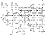
- Fig. 1 illustrates an example of a mixer arrangement suitable for dealing with two carrier frequencies. At top of Fig. 1 , it is also illustrated, from left to right, frequency diagrams for the received carriers or bands of carriers, the down-converted carriers or bands of carriers after the first down-conversion step, and finally the further down-converted and separated carriers or bands of carriers.
- the complex IF mixers preferably exhibit a substantial amount of harmonic rejection, otherwise undesired signals present around the harmonics of the IF LO frequency will be frequency-translated to fall on the desired signal.
- this provides issues for the use of traditional switched mixers that exhibit high conversion gain at harmonics of the LO, and at odd harmonics in particular.
- time-discrete harmonic rejection mixers that provide a high degree of harmonic rejection up to a certain harmonic index beyond which LO sampling images are present.
- a pre-filter can be used to attenuate signals appearing around those frequencies.
- the RF signals consist of two carriers being proximate in frequency, located at f c1 and f c2 , respectively.
- the frequency of the first LO signal driving the RF quadrature demodulator (RFLO) is set to a frequency, f RF,LO , at the middle of the two carriers.
- the two carriers can be down-converted to an IF frequency equal to half the carrier separation, f 1F , LO .
- the complex output of the quadrature demodulator makes it possible to distinguish the two carriers from each other as they will be located on either side of zero frequency, i.e. direct current (DC).
- selectivity can be implemented by IF filters, e.g. low-pass or band-pass filters to reduce signals levels at LO sampling image frequencies but also to reduce blocking signals to alleviate dynamic range requirements downstream in the receiver.
- the second conversion step is performed by complex IF mixers that aims to separate the two carriers while also down-converting them to baseband.
- This down-conversion is feasible by a second LO with a frequency set to f 1F , LO .
- the arrangement 100 comprises a first set of mixers 102, 104 receiving the RF signal from a low-noise amplifier, LNA, 101, wherein the mixers 102, 104 are arranged mutually in quadrature by phase offset of local oscillator (LO) signals LO I, RF , LO Q, RF provided to the mixers 102, 104.
- the LO signals LO I , RF , LO Q , RF are provided by a LO 106 which provides the LO signals at a frequency f RF, LO that is between the frequencies f c1 , f c2 of the two carriers or bands of carriers.
- the mixers 102, 104 outputs the IF signal as an in-phase IF signal and a quadrature-phase IF signal. These signals are preferably filtered by IF signal filters 108, 110, and then provided to a respective complex mixer 112, 114 for the respective carrier or band of carriers.
- the complex mixers 112, 114 performs the second down-conversion step using another LO signal LO I , IF , LO Q , IF provided from another LO 113, and the signals are preferably then filtered by channel selection filters 116, 118, 120, 122, and then digitised by analog-to-digital converters 124, 126, 128, 130. Further processing in digital domain (not shown) can then be made.
- the complex mixers 112, 114 of the arrangement 100 should preferably provide a substantial amount of harmonic rejection. Otherwise will undesired signals be present around harmonics of the frequency of the another LO such that they are frequency-translated to fall on the desired signal. This is troublesome since it is for a number of other reasons preferred to use switched mixers for the second mixing step. However, such switched mixers will provide high conversion gain at harmonics of the another LO and at odd harmonics in particular. Using time-discrete harmonic rejection mixers and/or using a pre-filter to attenuate signals around those frequencies may alleviate the problem.
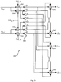
- Fig. 2 illustrates another example of a mixer arrangement 200 suitable for dealing with two carrier frequencies, presented here as background information.
- An LNA 201 provides an RF signal to mixers 202, 204 arranged mutually in quadrature by phase offset of local oscillator (LO) signals LO I , RF , LO Q , RF provided to the mixers 202, 204.
- LO local oscillator
- complex IF signals are generated accordingly and the IF signals are filtered by IF signal filters 208, 210, and then provided to a dual carrier complex mixer 213.
- the dual carrier complex mixer 213 performs the second down-conversion step using another LO signal LO I , IF , LO Q , IF provided from another LO and the signals are preferably then filtered by channel selection filters 216, 218, 220, 222, and then digitised by analog-to-digital converters 224, 226, 228, 230. Further processing in digital domain (not shown) can then be made.
- the dual carrier complex mixer 213 comprises mixer elements 232, 234, 236, 238 fed by respective of the in-phase and quadrature IF signals, and the LO signals LO I , IF , LO Q , IF , and summing elements 240, 242, 244, 246, wherein each mixer element 232, 234, 236, 238 provides the output signal to two of the summing elements 240, 242, 244, 246, wherein output signals from mixer elements 234, 236, which are mixing by the quadrature LO signal LO Q , IF , are connected to summing elements 240, 246 so as to provide inverse sign in the summing.
- a dual carrier complex mixer 300 can include means 302 for calibration of RF mixer imbalance, as illustrated in Fig. 3 .
- Each mixer element 332, 334, 336, 338 can provide its output to three summing elements 340, 342, 344, 346, i.e. each summing element has three inputs.
- the benefit is the improved imbalance calibration, but at the cost of increased circuitry.
- Fig. 4 illustrates an equivalent circuit 400 for a harmonic rejection mixer.
- the cross-coupled structure ensures that the input and output conductance of the mixer is constant with a variable ⁇ , as long as the load and source conductances, respectively, fulfil G L G S > > G m 2
- control sequences can be provided by a digital sequencer to produce a sinusoidal resembling transconductance.
- the discretisation into N unit cells means that the samples of the sinusoidal transconductance will be quantised such that g m ⁇ ⁇ NG u ⁇ N ⁇ 2 G u ⁇ N ⁇ 2 G u NG u
- the circuit area e.g. for integrated circuits
- consumption is non-negligible.
- the supporting circuitry required becomes large, i.e. each mixer may need a following buffer since it provides its output to three summing elements and a distribution network may consume space, although it adds benefits in terms of calibration of individual paths.
- accurate current splitting may not be guaranteed by just forwarding that current to three different current summing nodes. Having a buffer with virtual ground input and a voltage output which drives three resistive networks to generate three currents to the three different current summing nodes can solve this.
- each harmonic rejection mixer do not need to distribute its signal to more than one summing node, except for any issue about the calibration.
- the area can be made smaller if the buffers and associated circuitry can be omitted, i.e. at the expense of lost means for calibration, but the harmonic rejection mixer area will nevertheless double in size.
- the next task is to reduce layout area of the complex harmonic rejection mixer regardless of the IF mixer architecture being used. This is achieved by reuse of mixer unit cells between two harmonic rejection mixers operating in mutual quadrature.
- Fig. 7 shows (from top to bottom) cosine and sine waveforms, and also the sum of their absolute values.
- Fig. 13 illustrates for comparison corresponding time-discrete case, which will be further elucidated below.
- Mixer unit cells that is not used for in-phase harmonic rejection mixer can in part or completely be handed over to a quadrature phase harmonic rejection mixer as required, and vice versa.
- Input and output impedance of the complex IF mixer will not be affected since each node is attached to one in-phase mixer and one quadrature-phase mixer. Thus, the total impedance will be constant.
- the above demonstrated mixer unit cell sharing can be employed for example for the architectures discussed with reference to Fig. 1 or Fig. 2 .
- the mixer unit cell sharing can also be used in quadrature up and down conversion mixers if input and output impedance changes are managed.
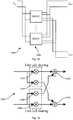
- Fig. 8 schematically illustrates a shared mixer unit cell, SMUC, which is described here for understanding but does not form part of the claimed invention.
- the SMUC 800 has an input where the signal V in is provided through transconductances G u to a sign switching network.
- output current is now output to one of two output ports, but never to both simultaneously.
- both ports have the switches located on the output side.
- the outputs can be terminated with low impedances, e.g. virtual ground, which will have the least impact on voltage modulation on the switches. If this is not a concern, the SMUC can have the switches on the input side with two input signal voltages to alternate between and one current output.
- Sign switching control signals S1 and S2 for respective ports are provided to the SMUC 800.
- control signals S1, S2 and A are provided from a sequencer and internal control signals S1a, S1b, S2a and S2b are generated therefrom in the SMUC 800.
- the control signals S1a, S1b, S2a and S2b can of course also be provided directly from the sequencer.
- the provision of the control signals from the sequencer to the SMUC can be affected by latency and/or other effects on the control signals.
- local flip-flops may be employed in or close to the SMUC 800 to synchronise all SMUCs with a common phase of a clock, wherein the generation of the respective physical control signals for the switches are generated accordingly anyway. A reduced number of signals can thus be preferred to be conveyed between the sequencer and the SMUC 800.
- Fig. 9 schematically illustrates a SMUC 900 which is presented here for understanding and does not form part of the claimed invention.
- the SMUC 900 has an input where the signal V in is provided through transconductances G u to a sign switching network.
- the sign switching network includes a sequential signal and path control.
- the control signals into the SMUC 900 are the same, i.e. S1, S2, A.
- the sequencer can of course provide control signals S and A directly.
- Fig. 10 illustrates a mixer arrangement 1000 comprising at least two harmonic rejection mixers using shared mixer unit cells 1002.
- all mixer unit cells are shared, which is of course not necessary as will be demonstrated with reference to Fig. 11 below.
- the thermometer code as demonstrated above for providing the sign switching signal to the respective SMUCs can be employed and can be provided by a sequencer (not shown), which preferably is controlled by one or more LOs.
- Locally clocked flip-flops can be provided in the SMUCs or by any circuitry in vicinity of them for each signal controlling a switch, respectively, if necessary to synchronise all SMUCs with a common phase of a clock due to the architecture of the mixer arrangement and/or other circuitry.
- An advantage of having all mixer unit cells shared is that a regular layout structure can be achieved, but which can be at the expense of longer signal routes for some output lines of the mixer arrangement 1000.
- Fig. 11 illustrates a mixer arrangement 1100 comprising at least two harmonic rejection mixers using both shared 1102 and non-shared 1104, 1106 mixer unit cells.
- the principles for this mixer arrangement 1100 are similar to what has been demonstrated above in sense of thermometer code, local flip-flops, assignment of switches, etc.
- An advantage of having a mix of shared and non-shared mixer unit cells can be that a design with comparably shorter signal routes for the outputs can be achieved, but at the expense of a more irregular layout structure.
- Fig. 12 illustrates an example of assignment of shared mixer unit cells in a complex harmonic rejection mixer 1200.
- a complex harmonic rejection mixer such as for example those demonstrated with reference to Fig. 1
- the harmonic rejection mixer 1200 features four harmonic rejection mixers 1232, 1234, 1236, and 1238 and includes two summing elements 1240, 1242.
- assigning the sharing can be such that the mixers having the in-phase IF signal as input to share SMUCs and that the mixers having the quadrature phase IF signal as input share their SMUCs.
- assigning the sharing can be such that the mixers having the in-phase IF signal as input to share SMUCs and that the mixers having the quadrature phase IF signal as input share their SMUCs.
- Similar advantage can be provided for a structure as those of the complex harmonic rejection mixers demonstrated with reference to any of Figs 2 and 3 .
- Fig. 13 illustrates graphs of time-discrete (from top to bottom) cosine and sine waveforms, and their absolute value sum.
- the graphs can be compared to the time-continuous graphs of Fig. 7 for finding correspondence (note the scales of level of sums).
- the illustrated time-discrete cosine and sine waveforms have an oversampling comprising 12 samples per LO period and are quantised to 20 amplitude levels, but this can of course be chosen differently.
- the degree of oversampling can be chosen such that switching in mixer unit cells, in the chosen structure, works well.
- the number of amplitude levels chosen has a relation to the number N of mixer unit cells used, i.e. to correspond to thermometer code.
- the quantisation can raise some issues to be considered when designing the mixer arrangement.
- the maximum of the sum is 28.
- the maximum sum of the absolute values of quantised amplitude levels may due to quantisation and sample position give a value exceeding a theoretical maximum level calculated based on time-continuous summed absolute values.
- one or two mixer unit cells more than such theoretical maximum level may be needed to be assigned when applying the thermometer code. The opposite will also be possible.
- a single harmonic rejection mixer needs N control signals S ⁇ 1:N>, from which Sbar ⁇ 1:N> can be derived.
- a first and a second harmonic rejection mixer would thus need 2N control signals.
- P control signals A ⁇ 1:P>, from which Abar ⁇ 1:P> can be derived to control whether the signal should be output to a first or second output of the SMUC, i.e. to be associated to the first or the second harmonic rejection mixer.
- a third state of the SMUC can be employed, e.g. a high impedance state, wherein for example redundant mixer unit cells which can be used for matching purposes etc. can be kept in reserve.
- Fig. 14 schematically illustrates a shared mixer unit cell, SMUC, 1400 according to an embodiment implementing such third state.
- the SMUC 1400 has an architecture similar to the one demonstrated with reference to Fig. 8 , but can also include a switch 1402 for short circuit of internal nodes to avoid a differential charge to build up when internal nodes are not connected to any output terminal, as will be understood to occur from the description below of control signals S1a, S1b, S2a and S2b for the respective switches of the SMUC 1400.
- control signals S1, S2, A and Y are provided from a sequencer and internal control signals S1a, S1b, S2a, S2b and S3 are generated therefrom in the SMUC 1400.
- the control signals S1a, S1b, S2a, S2b and S3 can of course also be provided directly from the sequencer.
- the provision of the control signals from the sequencer to the SMUC can be affected by latency and/or other effects on the control signals.
- flip-flops may be employed in or close to the SMUC 1400, wherein the generation of the physical control signals for the switches are generated accordingly anyway.
- the SMUC 1400 can thus be set in the third state, i.e. to functionally disconnect the SMUC by a high-impedance state.
- Fig. 15 schematically illustrates a SMUC 1500 according to an embodiment.
- the SMUC 1500 has an architecture similar to the one demonstrated with reference to Fig. 9 , but can also include a switch 1502 for short circuit of internal nodes to avoid a differential charge to build up when internal nodes are not connected to any output terminal, as will be understood to occur from the description below of control signals B and C for the respective switches of the SMUC 1500.
- the SMUC 1500 has an input where the signal V in is provided through transconductances G u to a sign switching network.
- the sign switching network includes a sequential signal and path control.
- the control signals into the SMUC 1500 are the same, i.e.
- the SMUC 1500 can thus be set in the third state, i.e. to functionally disconnect the SMUC by a high-impedance state.
- each harmonic rejection mixer When each harmonic rejection mixer is set to represent a certain transconductance and the sum of a first and second harmonic rejection mixer transconductance may not sum up to the maximum transconductance available from all mixer unit cells. Then, the remaining mixer unit cells should be configured to produce zero transconductance. This can be achieved by letting pairs of mixer unit cells produce transconductances with opposite signs to cancel each other. However, when unit cells are handed over from a first harmonic rejection mixer to a second harmonic rejection mixer, it is beneficial if they are handed over in pairs since a single mixer unit cell will always contribute with +G u or -G u , if not provided with a third state as demonstrated above. By this pair handling, the number P of control signals for A can be reduced to P/2.
- both the first and the second harmonic rejection mixer can have an odd number of mixer unit cells, accuracy can be improved since the number of transconductance levels can be doubled (cf. eq. 7) g m ⁇ ⁇ NG u ⁇ N ⁇ 1 G u ⁇ N ⁇ 1 G u NG u
- a particular advantage when having a SMUC capable of a third state, as demonstrated above, is when not both of a first and a second harmonic rejection mixer simultaneously benefits from an odd number of mixer unit cells.
- input and/or output impedance may in such cases vary a bit.
- the principle for handover of mixer unit cell pairs configured to produce zero transconductance contribution can be implemented in various ways. It may be based on that all such pairs are associated with either a first or a second harmonic rejection mixer; split equally between a first and second harmonic rejection mixer; or associated according to a random or more variable pattern. Ideally, handover of "unused" SMUC pairs will not have any impact on performance, but need to be considered anyway in a real implementation.
Landscapes
- Engineering & Computer Science (AREA)
- Power Engineering (AREA)
- Superheterodyne Receivers (AREA)
Description
- The present invention generally relates to a mixer arrangement for complex signal mixing, a radio circuit and a communication apparatus.
- Mixers are widely used in radio technology. A harmonic mixer, sometimes called a sampling mixer, mixes a signal with a pulse sequence representing the oscillator signal, wherein the pulse sequence has a fundamental frequency equal to a desired frequency translation frequency, and wherein switches can be used in the mixer. This has advantages in design in sense of power consumption and ability to operate at high frequencies. Due to the properties of the pulses, harmonics are generated. For alleviating this, and still keep the advantages of the harmonic mixer, the mixing can be performed at several mixer unit cells and the output from these are added, sometimes with opposite signs, i.e. a subtraction, to form an aggregate output signal more resembling the one of a time-continuous mixing with a sinusoid oscillator signal.
US 2009/0280762 A1 discloses a high-order harmonic rejection mixer using a current steering technique. The mixer generates a sinus-like signal by an input current generation unit generating and outputting an input current corresponding to an input signal, a first path circuit unit including a plurality of transistors having sources connected in common to the input current generation unit, a second path circuit including a plurality of transistors having sources connected in common to the input current generation unit, and a load unit connected to drains of the transistors of the first path circuit, while the drains of the transistors of the second path circuit are connected to ground. A local oscillator signal is phase shifted in steps corresponding to the plurality of transistors in the paths and are connected to the gates of the transistors with in-phase polarity to the transistors of the first circuit path and with opposite phase polarity to the transistors of the second circuit path. The transconductance of each of the transistors of the first path circuit is determined such that current passing through the transistors are turned on or off according to the phase-shifted oscillator signal to resemble a sinusoidal waveform. - Complex mixers provide a division of the mixed signal in an in-phase down-converted signal and a quadrature-phase down-converted signal. This can be provided arrangement for the quadrature-phase purpose, with oscillator signals thereto arranged in proper phase.
-
US 2011/0102051 disclosed a harmonic rejection mixer which includes a differential in-phase signal path and a differential quadrature signal path. A structure with a shared differential transconductor and mixing circuits connected thereto is suggested, wherein the mixers are controlled to selectively supply a shared transconductor output signal to the differential in-phase signal path and a differential quadrature signal path, respectively. -
US 2012/0049926 discloses a harmonic rejection mixer and combining outputs of a plurality of mixers connected in parallel to a rear stage of a plurality of gm elements. A common block with a structure of mixers connected in parallel to a gm element is also disclosed. -
WO 2005/091493 discloses a harmonic suppression mixer using a plurality of switching mixers each with a gain stage to produce a sinusoidal sum of the mixer outputs. It is also disclosed that switches can be used to isolate mixer signals in configurations where less than all of the mixers are used. - Mixers arranged to deal with two or more carriers are normally arranged by multiplying the number of mixers in the arrangements accordingly.
- When all the considerations above aggregates in a mixer design, the amount of circuitry rapidly expands. In circuit design, this requires a considerable layout size, which may cause one or more of the following problems: cost, size, power consumption, and signal path considerations (due to high-frequency issues).
- It is therefore a desire to alleviate such problems.
- An object of the invention is to at least alleviate the above stated problem. The present invention is based on the understanding that provision of a design of a versatile mixer unit cell together with an approach of letting mixers of a mixer arrangement share those mixer unit cells where appropriate can reduce the amount of circuitry.
- According to a first aspect, there is provided a mixer arrangement according to
independent claim 1. - The mixer arrangement may further comprise a third harmonic rejection mixer, and a fourth harmonic rejection mixer, wherein the third and the fourth rejection mixer share a second mixer unit cell comprising an input for receiving a signal to be mixed, an input for receiving control signals derived from a local oscillator signal, and one output for each of the third and fourth harmonic rejection mixers such that the mixer arrangement form a complex mixer.
- The arrangement may further comprise a signal generation unit arranged to generate the control signals. The signal generation unit may be arranged to provide a first set of binary control signals associated with sign switching for respective output of the shared mixer unit cell, and provide a second set of binary control signals associated with current output for respective output of the shared mixer unit cell such that current at any time instant is output to only one of the respective outputs. At least two mixer unit cells : not provided with a high impedance state may be paired such that the pair produces a zero aggregate output such that all mixer unit cells are always active. Transconductances of each of the harmonic rejection mixers may be assigned by their mixer unit cells such that transconductances sum up to provide resemblance to a sinusoidal waveform. For any of the shared mixer unit cells, the input for receiving a signal to be mixed may comprise a differential input comprising a first and a second input terminal, wherein the signal at respective input terminal is subject to a transconductance and switched to alternatively a first and a second output terminal of a differential output associated with one of the sharing harmonic rejection mixers such that the signal from the first input terminal is coupled to the first output terminal thereof when the signal from the second input terminal is coupled to the second output terminal thereof and the signal from the first input terminal is coupled to the second output terminal thereof when the signal from the second input terminal is coupled to the first output terminal thereof, and switched to alternatively a first and a second output terminal of a differential output associated with another of the sharing harmonic rejection mixers such that the signal from the first input terminal is coupled to the first output terminal thereof when the signal from the second input terminal is coupled to the second output terminal thereof and the signal from the first input terminal is coupled to the second output terminal thereof when the signal from the second input terminal is coupled to the first output terminal thereof, and wherein the alternating switching for respective harmonic rejection mixer is controlled based on a signal derived from the first and second sets of control signals. For any of the shared mixer unit cells, the input for receiving a signal to be mixed may comprise a differential input comprising a first and a second input terminal, wherein the signal at respective input terminal is subject to a transconductance and switched to alternatively a first and a second node such that the signal from the first input terminal is coupled to the first node when the signal from the second input terminal is coupled to the second node and the signal from the first input terminal is coupled to the second node when the signal from the second input terminal is coupled to the first node, and the signal at the first node is switched to alternatively a first output terminal of a differential output associated with one of the sharing harmonic rejection mixers and a first output terminal of a differential output associated with another of the sharing harmonic rejection mixers and the signal at the second node is switched to alternatively a second output terminal of a differential output associated with one of the sharing harmonic rejection mixers and a second output terminal of a differential output associated with another of the sharing harmonic rejection mixers, and wherein the alternating switching for respective node is controlled based on a respective signal derived from the first and second sets of control signals and the alternating switching to respective output terminals of the sharing harmonic rejection mixers is controlled based on the second set of control signals.
- Each harmonic rejection mixer may comprise an odd number of mixer unit cells.
- The mixer unit cells may comprise switches switched in dependence on the control signals and arranged to selectively thereupon connect the signal from input to output of respective mixer unit cell. Each mixer unit cell may comprise a switch controller arranged to receive the control signals and provide control of switch operation of the switches of respective mixer unit cell based on the received control signals.
- All mixer unit cells, respectively, may be structurally equally configured.
- According to a second aspect, there is provided a radio circuit comprising a mixer arrangement according to the first aspect.
- According to a third aspect, there is provided a communication apparatus comprising a radio circuit according to the second aspect.
- Other objectives, features and advantages of the present invention will appear from the following detailed disclosure, from the attached dependent claims as well as from the drawings. Generally, all terms used in the claims are to be interpreted according to their ordinary meaning in the technical field, unless explicitly defined otherwise herein. All references to "a/an/the [element, device, component, means, step, etc]" are to be interpreted openly as referring to at least one instance of said element, device, component, means, step, etc., unless explicitly stated otherwise.
- The above, as well as additional objects, features and advantages of the present invention, will be better understood through the following illustrative and non-limiting detailed description of preferred embodiments of the present invention, with reference to the appended drawings.
-
Fig. 1 illustrates an example of a mixer arrangement suitable for dealing with two carrier frequencies. -
Fig. 2 illustrates another example of a mixer arrangement suitable for dealing with two carrier frequencies. -
Fig. 3 illustrates further an example of a mixer arrangement suitable for dealing with two carrier frequencies, where controllable gain elements are used to compensate for mixer imbalance. -
Fig. 4 illustrates an equivalent circuit for a harmonic rejection mixer. -
Fig. 5 illustrates a mixer unit cell. -
Fig. 6 illustrates a mixer formed from mixer unit cells. -
Fig. 7 illustrates graphs of time-continuous sine and cosine waveforms, and their absolute value sum. -
Fig. 8 illustrates a mixer unit cell suitable for mixer unit cell sharing which does not form part of the claimed invention. -
Fig. 9 illustrates a mixer unit cell suitable for mixer unit cell sharing which does not form part of the claimed invention. -
Fig. 10 illustrates a mixer arrangement comprising two harmonic rejection mixers using shared mixer unit cells. -
Fig. 11 illustrates a mixer arrangement comprising two harmonic rejection mixers using both shared and non-shared mixer unit cells. -
Fig. 12 illustrates a complex harmonic rejection mixer using shared mixer unit cells. -
Fig. 13 illustrates graphs of time-discrete sine and cosine waveforms, and their absolute value sum. -
Fig. 14 illustrates a mixer unit cell suitable for mixer unit cell sharing according to the current invention. -
Fig. 15 illustrates a mixer unit cell suitable for mixer unit cell sharing according to the current invention. - For the understanding of the features of this disclosure and their benefits, an example of a double conversion receiver for reception of two carriers is used herein. However, as will be understood from the disclosure as a whole, the invention is not limited to this example. Instead, the features and benefits thereof can be employed to reduce consumption of circuit area and the from that caused issues for any mixer arrangement using harmonic rejection mixers. As also will be understood from the disclosure as a whole, benefits are also gained in sense of improvements in structured design of such arrangements.
- In a double-conversion receiver, a radio frequency (RF) signal is translated in two steps. When two carriers or two bands of carriers are received, and they are sufficiently close in frequency to enable down-conversion of them both using a single RF down-converter, they can be down-converted in a first step, and then in a second step they are simultaneously further down-converted and separated.
Fig. 1 illustrates an example of a mixer arrangement suitable for dealing with two carrier frequencies. At top ofFig. 1 , it is also illustrated, from left to right, frequency diagrams for the received carriers or bands of carriers, the down-converted carriers or bands of carriers after the first down-conversion step, and finally the further down-converted and separated carriers or bands of carriers. - The complex IF mixers preferably exhibit a substantial amount of harmonic rejection, otherwise undesired signals present around the harmonics of the IF LO frequency will be frequency-translated to fall on the desired signal. In other words, this provides issues for the use of traditional switched mixers that exhibit high conversion gain at harmonics of the LO, and at odd harmonics in particular. Furthermore, it may be possible to use time-discrete harmonic rejection mixers that provide a high degree of harmonic rejection up to a certain harmonic index beyond which LO sampling images are present. A pre-filter can be used to attenuate signals appearing around those frequencies.
- As indicated in the
Fig. 1 , the RF signals consist of two carriers being proximate in frequency, located at fc1 and fc2, respectively. The frequency of the first LO signal driving the RF quadrature demodulator (RFLO) is set to a frequency, fRF,LO, at the middle of the two carriers. - The two carriers can be down-converted to an IF frequency equal to half the carrier separation, f1F,LO. The complex output of the quadrature demodulator makes it possible to distinguish the two carriers from each other as they will be located on either side of zero frequency, i.e. direct current (DC). At this point selectivity can be implemented by IF filters, e.g. low-pass or band-pass filters to reduce signals levels at LO sampling image frequencies but also to reduce blocking signals to alleviate dynamic range requirements downstream in the receiver.
- The second conversion step is performed by complex IF mixers that aims to separate the two carriers while also down-converting them to baseband. This down-conversion is feasible by a second LO with a frequency set to f1F,LO. Ideally, we might consider the complex-valued IF signal at the input to be represented by

- The purpose of the IF mixers is to multiply this input signal by two phases,


- In the given example, a complex intermediate frequency (IF) based architecture is illustrated. The
arrangement 100 comprises a first set ofmixers mixers mixers LO 106 which provides the LO signals at a frequency fRF, LO that is between the frequencies fc1, fc2 of the two carriers or bands of carriers. Themixers complex mixer complex mixers LO 113, and the signals are preferably then filtered by channel selection filters 116, 118, 120, 122, and then digitised by analog-to-digital converters - The
complex mixers arrangement 100 should preferably provide a substantial amount of harmonic rejection. Otherwise will undesired signals be present around harmonics of the frequency of the another LO such that they are frequency-translated to fall on the desired signal. This is troublesome since it is for a number of other reasons preferred to use switched mixers for the second mixing step. However, such switched mixers will provide high conversion gain at harmonics of the another LO and at odd harmonics in particular. Using time-discrete harmonic rejection mixers and/or using a pre-filter to attenuate signals around those frequencies may alleviate the problem. -
Fig. 2 illustrates another example of amixer arrangement 200 suitable for dealing with two carrier frequencies, presented here as background information. AnLNA 201 provides an RF signal tomixers mixers 202, 204.Similar to the example given with reference toFig. 1 , complex IF signals are generated accordingly and the IF signals are filtered by IF signal filters 208, 210, and then provided to a dualcarrier complex mixer 213. The dualcarrier complex mixer 213 performs the second down-conversion step using another LO signal LOI, IF, LOQ, IF provided from another LO and the signals are preferably then filtered by channel selection filters 216, 218, 220, 222, and then digitised by analog-to-digital converters carrier complex mixer 213 comprisesmixer elements elements mixer element elements mixer elements elements - A dual
carrier complex mixer 300 can include means 302 for calibration of RF mixer imbalance, as illustrated inFig. 3 . Eachmixer element elements - For the further understanding of harmonic rejection mixers,
Fig. 4 illustrates anequivalent circuit 400 for a harmonic rejection mixer. Theequivalent circuit 400 comprises a voltage source 402 which drives a resistive voltage-to-current conversion with single-ended transconductance, i.e. gain, given by
- The cross-coupled structure ensures that the input and output conductance of the mixer is constant with a variable α, as long as the load and source conductances, respectively, fulfil

- A harmonic rejection mixer with time-continuous operation according to what is demonstrated above is not recommendable with regards to implementation in commercially feasible products. Instead, a time-discrete solution based on the use of a
mixer unit cell 500, as depicted inFig. 5 , that includes a pair ofresistors network 506 controlled by signals S and Sbar, where Sbar is the logical inverse of S. - A
vector 600 ofN unit cells 602 are connected in parallel, as depicted inFig. 6 , and switches of the sign-switching networks are controlled to generate a time-discrete sinusoidal resembling transconductance. That is, the effective LO waveform is represented by a thermometer code S<1:N>, where S can takevalues 
- These control sequences can be provided by a digital sequencer to produce a sinusoidal resembling transconductance.
- The discretisation into N unit cells means that the samples of the sinusoidal transconductance will be quantised such that

- It is possible to use a very limited number of unit cells and yet obtain very low levels of quantization. This can be achieved by using an integer number of samples per LO period and use the number of unit cells for max gm that leads to the highest spectral purity, i.e. minimised harmonic content and therefore maximised harmonic rejection.
- Coming to this point, the circuit area, e.g. for integrated circuits, consumption is non-negligible. When saving area by using four harmonic rejection mixers for reception of two carriers, the supporting circuitry required becomes large, i.e. each mixer may need a following buffer since it provides its output to three summing elements and a distribution network may consume space, although it adds benefits in terms of calibration of individual paths. Here, when the mixer has a current output, accurate current splitting may not be guaranteed by just forwarding that current to three different current summing nodes. Having a buffer with virtual ground input and a voltage output which drives three resistive networks to generate three currents to the three different current summing nodes can solve this. However, in a solution with separate complex mixers, each harmonic rejection mixer do not need to distribute its signal to more than one summing node, except for any issue about the calibration. When using eight harmonic rejection mixers, i.e. one complex IF mixer for each carrier, the area can be made smaller if the buffers and associated circuitry can be omitted, i.e. at the expense of lost means for calibration, but the harmonic rejection mixer area will nevertheless double in size. Thus, the next task is to reduce layout area of the complex harmonic rejection mixer regardless of the IF mixer architecture being used. This is achieved by reuse of mixer unit cells between two harmonic rejection mixers operating in mutual quadrature. While the peak transconductance value of one of the harmonic rejection mixers will be NGu, the peak of the absolute sum of the two harmonic rejection mixers will be approximately

Fig. 7 which shows (from top to bottom) cosine and sine waveforms, and also the sum of their absolute values. Next toFig. 7, Fig. 13 illustrates for comparison corresponding time-discrete case, which will be further elucidated below. - Mixer unit cells that is not used for in-phase harmonic rejection mixer can in part or completely be handed over to a quadrature phase harmonic rejection mixer as required, and vice versa. Input and output impedance of the complex IF mixer will not be affected since each node is attached to one in-phase mixer and one quadrature-phase mixer. Thus, the total impedance will be constant.
- The above demonstrated mixer unit cell sharing can be employed for example for the architectures discussed with reference to
Fig. 1 orFig. 2 . The mixer unit cell sharing can also be used in quadrature up and down conversion mixers if input and output impedance changes are managed. -
Fig. 8 schematically illustrates a shared mixer unit cell, SMUC, which is described here for understanding but does not form part of the claimed invention. TheSMUC 800 has an input where the signal Vin is provided through transconductances Gu to a sign switching network. In addition to providing sign control as for a regular mixer unit cell, e.g. as demonstrated with reference toFig. 5 , output current is now output to one of two output ports, but never to both simultaneously. Here, both ports have the switches located on the output side. The outputs can be terminated with low impedances, e.g. virtual ground, which will have the least impact on voltage modulation on the switches. If this is not a concern, the SMUC can have the switches on the input side with two input signal voltages to alternate between and one current output. - Sign switching control signals S1 and S2 for respective ports are provided to the
SMUC 800. An arbitration signal A also provided to theSMUC 800 will ensure that the current is not output to both the output ports simultaneously by therelations 


Fig. 8 , it is depicted that control signals S1, S2 and A are provided from a sequencer and internal control signals S1a, S1b, S2a and S2b are generated therefrom in theSMUC 800. However, the control signals S1a, S1b, S2a and S2b can of course also be provided directly from the sequencer. Further, the provision of the control signals from the sequencer to the SMUC can be affected by latency and/or other effects on the control signals. In such cases, local flip-flops may be employed in or close to theSMUC 800 to synchronise all SMUCs with a common phase of a clock, wherein the generation of the respective physical control signals for the switches are generated accordingly anyway. A reduced number of signals can thus be preferred to be conveyed between the sequencer and theSMUC 800. -
Fig. 9 schematically illustrates aSMUC 900 which is presented here for understanding and does not form part of the claimed invention. TheSMUC 900 has an input where the signal Vin is provided through transconductances Gu to a sign switching network. Here, the sign switching network includes a sequential signal and path control. For comparison with theSMUC 800 demonstrated with reference toFig. 8 , the control signals into theSMUC 900 are the same, i.e. S1, S2, A. However, according to the discussion above, the sequencer can of course provide control signals S and A directly. The relation between S1 and S2 and S is, where the addition of "bar" also here means the logical inverse, S=S1 x A + S2 x Abar. -
Fig. 10 illustrates amixer arrangement 1000 comprising at least two harmonic rejection mixers using sharedmixer unit cells 1002. Here, according to the illustration, all mixer unit cells are shared, which is of course not necessary as will be demonstrated with reference toFig. 11 below. The thermometer code as demonstrated above for providing the sign switching signal to the respective SMUCs can be employed and can be provided by a sequencer (not shown), which preferably is controlled by one or more LOs. Locally clocked flip-flops can be provided in the SMUCs or by any circuitry in vicinity of them for each signal controlling a switch, respectively, if necessary to synchronise all SMUCs with a common phase of a clock due to the architecture of the mixer arrangement and/or other circuitry. - An advantage of having all mixer unit cells shared is that a regular layout structure can be achieved, but which can be at the expense of longer signal routes for some output lines of the
mixer arrangement 1000. -
Fig. 11 illustrates amixer arrangement 1100 comprising at least two harmonic rejection mixers using both shared 1102 and non-shared 1104, 1106 mixer unit cells. The principles for thismixer arrangement 1100 are similar to what has been demonstrated above in sense of thermometer code, local flip-flops, assignment of switches, etc. - An advantage of having a mix of shared and non-shared mixer unit cells can be that a design with comparably shorter signal routes for the outputs can be achieved, but at the expense of a more irregular layout structure.
-
Fig. 12 illustrates an example of assignment of shared mixer unit cells in a complexharmonic rejection mixer 1200. For a complex harmonic rejection mixer, such as for example those demonstrated with reference toFig. 1 , there are four harmonic rejection mixers. Theharmonic rejection mixer 1200 features fourharmonic rejection mixers elements Figs 2 and3 . -
Fig. 13 illustrates graphs of time-discrete (from top to bottom) cosine and sine waveforms, and their absolute value sum. The graphs can be compared to the time-continuous graphs ofFig. 7 for finding correspondence (note the scales of level of sums). The illustrated time-discrete cosine and sine waveforms have an oversampling comprising 12 samples per LO period and are quantised to 20 amplitude levels, but this can of course be chosen differently. Here, the degree of oversampling can be chosen such that switching in mixer unit cells, in the chosen structure, works well. The number of amplitude levels chosen has a relation to the number N of mixer unit cells used, i.e. to correspond to thermometer code. However, it will be discussed below that the quantisation can raise some issues to be considered when designing the mixer arrangement. - In the depicted example, the maximum of the sum is 28. Depending on the chosen number of samples per LO period and the quantisation of the amplitude level, the maximum sum of the absolute values of quantised amplitude levels may due to quantisation and sample position give a value exceeding a theoretical maximum level calculated based on time-continuous summed absolute values. Thus, one or two mixer unit cells more than such theoretical maximum level may be needed to be assigned when applying the thermometer code. The opposite will also be possible.
- Thus, a single harmonic rejection mixer needs N control signals S <1:N>, from which Sbar <1:N> can be derived. A first and a second harmonic rejection mixer would thus need 2N control signals. When the first and the second harmonic rejection mixer shares P mixer unit cells, there is further needed P control signals A<1:P>, from which Abar <1:P> can be derived, to control whether the signal should be output to a first or second output of the SMUC, i.e. to be associated to the first or the second harmonic rejection mixer.
- In accordance with the current invention, for a case where not all SMUCs are active, i.e. not being assigned to either the first or the second harmonic rejection mixer, a third state of the SMUC can be employed, e.g. a high impedance state, wherein for example redundant mixer unit cells which can be used for matching purposes etc. can be kept in reserve.
-
Fig. 14 schematically illustrates a shared mixer unit cell, SMUC, 1400 according to an embodiment implementing such third state. TheSMUC 1400 has an architecture similar to the one demonstrated with reference toFig. 8 , but can also include aswitch 1402 for short circuit of internal nodes to avoid a differential charge to build up when internal nodes are not connected to any output terminal, as will be understood to occur from the description below of control signals S1a, S1b, S2a and S2b for the respective switches of theSMUC 1400. Further, an additional signal Y from the sequencer is provided, and the internal control signals for the switches are provided according to therelations 


Fig. 14 , it is depicted that control signals S1, S2, A and Y are provided from a sequencer and internal control signals S1a, S1b, S2a, S2b and S3 are generated therefrom in theSMUC 1400. However, the control signals S1a, S1b, S2a, S2b and S3 can of course also be provided directly from the sequencer. Further, the provision of the control signals from the sequencer to the SMUC can be affected by latency and/or other effects on the control signals. In such cases, flip-flops may be employed in or close to theSMUC 1400, wherein the generation of the physical control signals for the switches are generated accordingly anyway. A reduced number of signals can thus be preferred to be conveyed between the sequencer and theSMUC 1400. By the signal Y, theSMUC 1400 can thus be set in the third state, i.e. to functionally disconnect the SMUC by a high-impedance state. -
Fig. 15 schematically illustrates aSMUC 1500 according to an embodiment. TheSMUC 1500 has an architecture similar to the one demonstrated with reference toFig. 9 , but can also include aswitch 1502 for short circuit of internal nodes to avoid a differential charge to build up when internal nodes are not connected to any output terminal, as will be understood to occur from the description below of control signals B and C for the respective switches of theSMUC 1500.. TheSMUC 1500 has an input where the signal Vin is provided through transconductances Gu to a sign switching network. Here, the sign switching network includes a sequential signal and path control. For comparison with theSMUC 1400 demonstrated with reference toFig. 14 , the control signals into theSMUC 1500 are the same, i.e. S1, S2, A and Y. However, according to the discussion above, the sequencer can of course provide control signals S, B, C and SY directly. The relations between S1, S2, A and Y and the control signals S, B, C and SY are


- By the signal Y, the
SMUC 1500 can thus be set in the third state, i.e. to functionally disconnect the SMUC by a high-impedance state. - When each harmonic rejection mixer is set to represent a certain transconductance and the sum of a first and second harmonic rejection mixer transconductance may not sum up to the maximum transconductance available from all mixer unit cells. Then, the remaining mixer unit cells should be configured to produce zero transconductance. This can be achieved by letting pairs of mixer unit cells produce transconductances with opposite signs to cancel each other. However, when unit cells are handed over from a first harmonic rejection mixer to a second harmonic rejection mixer, it is beneficial if they are handed over in pairs since a single mixer unit cell will always contribute with +Gu or -Gu, if not provided with a third state as demonstrated above. By this pair handling, the number P of control signals for A can be reduced to P/2.
- For a case where both the first and the second harmonic rejection mixer can have an odd number of mixer unit cells, accuracy can be improved since the number of transconductance levels can be doubled (cf. eq. 7)

- A particular advantage when having a SMUC capable of a third state, as demonstrated above, is when not both of a first and a second harmonic rejection mixer simultaneously benefits from an odd number of mixer unit cells. However, input and/or output impedance may in such cases vary a bit.
- The principle for handover of mixer unit cell pairs configured to produce zero transconductance contribution, as discussed above, can be implemented in various ways. It may be based on that all such pairs are associated with either a first or a second harmonic rejection mixer; split equally between a first and second harmonic rejection mixer; or associated according to a random or more variable pattern. Ideally, handover of "unused" SMUC pairs will not have any impact on performance, but need to be considered anyway in a real implementation.
- The invention has mainly been described above with reference to a few embodiments. From this disclosure it can be understood that considerable layout area savings can be done utilising the principles demonstrated above. As a further advantage, the smaller layout area needed also provides for shorter paths for clock signals and other signals with corresponding benefits as reduced power dissipation, latency, interference sensitivity, etc. In this disclosure, some implementations where the embodiments can be beneficial have been indicated. However, as is readily appreciated by a person skilled in the art, other embodiments and implementations than the ones disclosed above are equally possible within the scope of the invention, as defined by the appended patent claims.
Claims (14)
- A mixer arrangement (112, 114, 213, 300, 1000, 1100, 1200) for complex signal mixing comprising
a first harmonic rejection mixer (232, 332, 1232); and
a second harmonic rejection mixer (234, 334, 1234), wherein
each of the harmonic rejection mixers comprises a plurality of mixer unit cells (500, 602, 800, 900, 1002, 1102, 1104, 1106, 1400, 1500) connected in parallel, wherein each mixer unit cell comprises a differential input, transconductance elements connected to the corresponding differential inputs, and a switching network arranged to switch signals from the transconductance elements to a differential output,
the first and the second harmonic rejection mixers having a mutual quadrature phase relationship, and
wherein the first and the second harmonic rejection mixers share a plurality of mixer unit cells (800, 900, 1002, 1102, 1400, 1500) among the mixer unit cells (500, 602, 800, 900, 1002, 1102, 1104, 1106, 1400, 1500), wherein each shared mixer unit cell (800, 900, 1002, 1102, 1400, 1500) comprisesan input for receiving a signal to be mixed (Vin),an input for receiving control signals (S1, S2) derived from a local oscillator signal, andone output for each of the first and second harmonic rejection mixers, andcharacterised in that the control signals comprise an additional signal (Y) configured for causing the switching network to put the shared mixer unit cell (1400, 1500) in a high impedance state in which the shared mixer unit cell is functionally disconnected from the first and second harmonic rejection mixers. - The mixer arrangement according to claim 1, further comprising
a third harmonic rejection mixer (236, 336, 1236); and
a fourth harmonic rejection mixer (238, 338, 1238), wherein
the third and the fourth rejection mixer share a second mixer unit cell (800, 900, 1002, 1102, 1400, 1500) comprisingan input for receiving a signal to be mixed,an input for receiving control signals derived from a local oscillator signal, andone output for each of the third and fourth harmonic rejection mixers such that the mixer arrangement forms a complex mixer. - The mixer arrangement according to any of claims 1 or 2, further comprising a signal generation unit arranged to generate the control signals.
- The mixer arrangement according to claim 3, wherein the signal generation unit is arranged to provide a first set of binary control signals associated with polarity switching for respective output of the shared mixer unit cell, and provide a second set of binary control signals associated with current output for respective output of the shared mixer unit cell such that current at any time instant is output to only one of the respective outputs.
- The mixer arrangement according to claim 4, wherein at least two mixer unit cells not provided with the high impedance state are paired such that mixer unit cells of the pair cancel each other to produce a zero aggregate output such that both mixer unit cells of the pair are always active.
- The mixer arrangement according to any of claims 4 or 5, wherein, for any of the shared mixer unit cells (800, 1400), the input for receiving a signal to be mixed comprises a differential input comprising a first and a second input terminal, wherein the signal at respective input terminal is subject to a transconductance and switched to alternatively a first and a second output terminal of a differential output associated with one of the sharing harmonic rejection mixers such that the signal from the first input terminal is coupled to the first output terminal thereof when the signal from the second input terminal is coupled to the second output terminal thereof and the signal from the first input terminal is coupled to the second output terminal thereof when the signal from the second input terminal is coupled to the first output terminal thereof, and switched to alternatively a first and a second output terminal of a differential output associated with another of the sharing harmonic rejection mixers such that the signal from the first input terminal is coupled to the first output terminal thereof when the signal from the second input terminal is coupled to the second output terminal thereof and the signal from the first input terminal is coupled to the second output terminal thereof when the signal from the second input terminal is coupled to the first output terminal thereof, and
wherein the alternating switching for respective harmonic rejection mixer is controlled based on a signal derived from the first and second sets of control signals. - The mixer arrangement according to any of claims 3 to 6, wherein transconductances of each of the harmonic rejection mixers are assigned by their mixer unit cells such that transconductances sum up to provide resemblance to a sinusoidal waveform.
- The mixer arrangement according to any of claims 4 to 6, wherein, for any of the shared mixer unit cells (900, 1500), the input for receiving a signal to be mixed comprises a differential input comprising a first and a second input terminal, wherein the signal at respective input terminal is subject to a transconductance and switched to alternatively a first and a second node such that the signal from the first input terminal is coupled to the first node when the signal from the second input terminal is coupled to the second node and the signal from the first input terminal is coupled to the second node when the signal from the second input terminal is coupled to the first node, and the signal at the first node is switched to alternatively a first output terminal of a differential output associated with one of the sharing harmonic rejection mixers and a first output terminal of a differential output associated with another of the sharing harmonic rejection mixers and the signal at the second node is switched to alternatively a second output terminal of a differential output associated with one of the sharing harmonic rejection mixers and a second output terminal of a differential output associated with another of the sharing harmonic rejection mixers, and
wherein the alternating switching for respective node is controlled based on a respective signal derived from the first and second sets of control signals and the alternating switching to respective output terminals of the sharing harmonic rejection mixers is controlled based on the second set of control signals. - The mixer arrangement according to any of claims 1 to 8, wherein each harmonic rejection mixer comprises an odd number of mixer unit cells.
- The mixer arrangement according to any of claims 1 to 9, wherein the mixer unit cells comprises switches switched in dependence on the control signals and arranged to selectively thereupon connect the signal from input to output of respective mixer unit cell.
- The mixer arrangement according to claim 10, wherein each mixer unit cell comprises a switch controller arranged to receive the control signals and provide control of switch operation of the switches of respective mixer unit cell based on the received control signals.
- The mixer arrangement according to any of claims 1 to 11, wherein all mixer unit cells, respectively, are structurally equally configured.
- A radio circuit comprising a mixer arrangement according to any of claims 1 to 12.
- A communication apparatus comprising a radio circuit according to claim 13.
Priority Applications (3)
| Application Number | Priority Date | Filing Date | Title |
|---|---|---|---|
| EP12164771.3A EP2654202B1 (en) | 2012-04-19 | 2012-04-19 | Harmonic Rejection Mixer Arrangement |
| US14/394,956 US9450538B2 (en) | 2012-04-19 | 2013-04-03 | Harmonic rejection mixer arrangement |
| PCT/EP2013/057011 WO2013156305A1 (en) | 2012-04-19 | 2013-04-03 | Harmonic rejection mixer arrangement |
Applications Claiming Priority (1)
| Application Number | Priority Date | Filing Date | Title |
|---|---|---|---|
| EP12164771.3A EP2654202B1 (en) | 2012-04-19 | 2012-04-19 | Harmonic Rejection Mixer Arrangement |
Publications (2)
| Publication Number | Publication Date |
|---|---|
| EP2654202A1 EP2654202A1 (en) | 2013-10-23 |
| EP2654202B1 true EP2654202B1 (en) | 2020-01-01 |
Family
ID=46027675
Family Applications (1)
| Application Number | Title | Priority Date | Filing Date |
|---|---|---|---|
| EP12164771.3A Active EP2654202B1 (en) | 2012-04-19 | 2012-04-19 | Harmonic Rejection Mixer Arrangement |
Country Status (3)
| Country | Link |
|---|---|
| US (1) | US9450538B2 (en) |
| EP (1) | EP2654202B1 (en) |
| WO (1) | WO2013156305A1 (en) |
Families Citing this family (3)
| Publication number | Priority date | Publication date | Assignee | Title |
|---|---|---|---|---|
| CN103828244B (en) * | 2012-06-21 | 2016-03-02 | 华为技术有限公司 | Super Heterodyne Receiver and method of reseptance |
| US9529380B1 (en) | 2015-08-04 | 2016-12-27 | Qualcomm Incorporated | Local oscillator signal generation circuit with harmonic current rejection |
| US10620659B2 (en) | 2017-04-05 | 2020-04-14 | International Business Machines Corporation | Clock network analysis using harmonic balance |
Family Cites Families (15)
| Publication number | Priority date | Publication date | Assignee | Title |
|---|---|---|---|---|
| KR100519876B1 (en) | 2004-01-30 | 2005-10-10 | 삼성전자주식회사 | Mixer Circuit used for Direct Conversion with improved IP2 and Direct Conversion Transceiver using the Mixer Circuit |
| US7519348B2 (en) * | 2004-03-12 | 2009-04-14 | Rf Magic, Inc. | Harmonic suppression mixer and tuner |
| US7509110B2 (en) | 2005-03-14 | 2009-03-24 | Broadcom Corporation | High-order harmonic rejection mixer using multiple LO phases |
| US7385429B1 (en) * | 2005-05-31 | 2008-06-10 | Altera Corporation | Charge pump with reduced current mismatch |
| US7532874B2 (en) | 2005-11-09 | 2009-05-12 | Texas Instruments Incorporated | Offset balancer, method of balancing an offset and a wireless receiver employing the balancer and the method |
| US7826816B2 (en) | 2006-07-11 | 2010-11-02 | Qualcomm Incorporated | Systems, methods, and apparatus for frequency conversion |
| US8072255B2 (en) | 2008-01-07 | 2011-12-06 | Qualcomm Incorporated | Quadrature radio frequency mixer with low noise and low conversion loss |
| KR20090117537A (en) | 2008-05-09 | 2009-11-12 | 삼성전기주식회사 | Higher Harmonic Elimination Mixer with Current Steering |
| EP2141819A1 (en) | 2008-07-04 | 2010-01-06 | Telefonaktiebolaget LM Ericsson (publ) | Signal processing device and method |
| WO2010087199A1 (en) * | 2009-01-29 | 2010-08-05 | パナソニック株式会社 | Harmonic rejection mixer |
| US8378733B2 (en) * | 2009-10-30 | 2013-02-19 | Stmicroelectronics Design & Application Gmbh | Harmonic rejection mixer |
| EP2333949B1 (en) | 2009-12-11 | 2016-06-29 | Telefonaktiebolaget LM Ericsson (publ) | Mixer arrangement |
| EP2434640B1 (en) | 2010-09-24 | 2012-12-05 | Telefonaktiebolaget L M Ericsson (PUBL) | Correction of imbalances in a complex intermediate frequency mixer |
| US8624660B2 (en) * | 2012-04-19 | 2014-01-07 | Telefonaktiebolaget Lm Ericsson (Publ) | Method and apparatus for mixer-based harmonic rejection |
| US9017197B2 (en) * | 2012-05-16 | 2015-04-28 | Dayco Ip Holdings, Llc | Hydraulic damping mechanism and use for belt tensioning |
-
2012
- 2012-04-19 EP EP12164771.3A patent/EP2654202B1/en active Active
-
2013
- 2013-04-03 US US14/394,956 patent/US9450538B2/en active Active
- 2013-04-03 WO PCT/EP2013/057011 patent/WO2013156305A1/en active Application Filing
Non-Patent Citations (1)
| Title |
|---|
| None * |
Also Published As
| Publication number | Publication date |
|---|---|
| US20150070071A1 (en) | 2015-03-12 |
| EP2654202A1 (en) | 2013-10-23 |
| WO2013156305A1 (en) | 2013-10-24 |
| US9450538B2 (en) | 2016-09-20 |
Similar Documents
| Publication | Publication Date | Title |
|---|---|---|
| US8867671B2 (en) | Conversion circuit for converting complex analog signal into digital representation | |
| US7421259B2 (en) | RF mixer with high local oscillator linearity using multiple local oscillator phases | |
| Crols et al. | Low-IF topologies for high-performance analog front ends of fully integrated receivers | |
| US8165538B2 (en) | Systems and methods for implementing a harmonic rejection mixer | |
| EP2408118B1 (en) | Conversion system | |
| US7986192B2 (en) | Harmonic rejection mixer and harmonic rejection mixing method | |
| EP2191566B1 (en) | Harmonic rejection mixer unit and method for performing a harmonic rejection mixing | |
| CN100539653C (en) | Multi-band television tuner and associated method | |
| EP3286833B1 (en) | Method and apparatus for mixing signals using charge canceller circuit | |
| EP2654202B1 (en) | Harmonic Rejection Mixer Arrangement | |
| JP5821846B2 (en) | Frequency converter and receiver using the same | |
| KR100836950B1 (en) | Harmonic mixer | |
| US8378733B2 (en) | Harmonic rejection mixer | |
| JP5790650B2 (en) | Frequency converter and receiver using the same | |
| EP3105854B1 (en) | A charge sharing filter | |
| US20060252396A1 (en) | Phase generator using polyphase architecture | |
| US9209750B2 (en) | Harmonic rejection mixer | |
| Ugajin et al. | Image-rejection-performance assessment of double-conversion wireless receiver with 3-phase complex filter using montecarlo simulation | |
| Yamaji et al. | A 6-phase harmonic rejection down-converter with digital assist | |
| Ugajin et al. | An (N+N 2)-Mixer Architecture for a High-Image-Rejection Wireless Receiver with an N-Phase Active Complex Filter | |
| WO2009059831A2 (en) | Mixing apparatus | |
| WO2020239233A1 (en) | Radio frequency receiver and method for down-converting signals to baseband signal components | |
| da Costa Malheiro | Polyphase Filter with Parametric Tuning | |
| EP2980987B1 (en) | Frequency down-conversion | |
| JP2015084520A (en) | Bandpass filter |
Legal Events
| Date | Code | Title | Description |
|---|---|---|---|
| PUAI | Public reference made under article 153(3) epc to a published international application that has entered the european phase |
Free format text: ORIGINAL CODE: 0009012 |
|
| 17P | Request for examination filed |
Effective date: 20130816 |
|
| AK | Designated contracting states |
Kind code of ref document: A1 Designated state(s): AL AT BE BG CH CY CZ DE DK EE ES FI FR GB GR HR HU IE IS IT LI LT LU LV MC MK MT NL NO PL PT RO RS SE SI SK SM TR |
|
| AX | Request for extension of the european patent |
Extension state: BA ME |
|
| RBV | Designated contracting states (corrected) |
Designated state(s): AL AT BE BG CH CY CZ DE DK EE ES FI FR GB GR HR HU IE IS IT LI LT LU LV MC MK MT NL NO PL PT RO RS SE SI SK SM TR |
|
| STAA | Information on the status of an ep patent application or granted ep patent |
Free format text: STATUS: EXAMINATION IS IN PROGRESS |
|
| 17Q | First examination report despatched |
Effective date: 20171013 |
|
| GRAP | Despatch of communication of intention to grant a patent |
Free format text: ORIGINAL CODE: EPIDOSNIGR1 |
|
| STAA | Information on the status of an ep patent application or granted ep patent |
Free format text: STATUS: GRANT OF PATENT IS INTENDED |
|
| INTG | Intention to grant announced |
Effective date: 20191011 |
|
| GRAS | Grant fee paid |
Free format text: ORIGINAL CODE: EPIDOSNIGR3 |
|
| GRAA | (expected) grant |
Free format text: ORIGINAL CODE: 0009210 |
|
| STAA | Information on the status of an ep patent application or granted ep patent |
Free format text: STATUS: THE PATENT HAS BEEN GRANTED |
|
| AK | Designated contracting states |
Kind code of ref document: B1 Designated state(s): AL AT BE BG CH CY CZ DE DK EE ES FI FR GB GR HR HU IE IS IT LI LT LU LV MC MK MT NL NO PL PT RO RS SE SI SK SM TR |
|
| REG | Reference to a national code |
Ref country code: GB Ref legal event code: FG4D |
|
| REG | Reference to a national code |
Ref country code: CH Ref legal event code: EP Ref country code: AT Ref legal event code: REF Ref document number: 1221057 Country of ref document: AT Kind code of ref document: T Effective date: 20200115 |
|
| REG | Reference to a national code |
Ref country code: IE Ref legal event code: FG4D |
|
| REG | Reference to a national code |
Ref country code: DE Ref legal event code: R096 Ref document number: 602012066837 Country of ref document: DE |
|
| REG | Reference to a national code |
Ref country code: NL Ref legal event code: MP Effective date: 20200101 |
|
| REG | Reference to a national code |
Ref country code: LT Ref legal event code: MG4D |
|
| PG25 | Lapsed in a contracting state [announced via postgrant information from national office to epo] |
Ref country code: FI Free format text: LAPSE BECAUSE OF FAILURE TO SUBMIT A TRANSLATION OF THE DESCRIPTION OR TO PAY THE FEE WITHIN THE PRESCRIBED TIME-LIMIT Effective date: 20200101 Ref country code: NO Free format text: LAPSE BECAUSE OF FAILURE TO SUBMIT A TRANSLATION OF THE DESCRIPTION OR TO PAY THE FEE WITHIN THE PRESCRIBED TIME-LIMIT Effective date: 20200401 Ref country code: PT Free format text: LAPSE BECAUSE OF FAILURE TO SUBMIT A TRANSLATION OF THE DESCRIPTION OR TO PAY THE FEE WITHIN THE PRESCRIBED TIME-LIMIT Effective date: 20200527 Ref country code: CZ Free format text: LAPSE BECAUSE OF FAILURE TO SUBMIT A TRANSLATION OF THE DESCRIPTION OR TO PAY THE FEE WITHIN THE PRESCRIBED TIME-LIMIT Effective date: 20200101 Ref country code: RS Free format text: LAPSE BECAUSE OF FAILURE TO SUBMIT A TRANSLATION OF THE DESCRIPTION OR TO PAY THE FEE WITHIN THE PRESCRIBED TIME-LIMIT Effective date: 20200101 Ref country code: NL Free format text: LAPSE BECAUSE OF FAILURE TO SUBMIT A TRANSLATION OF THE DESCRIPTION OR TO PAY THE FEE WITHIN THE PRESCRIBED TIME-LIMIT Effective date: 20200101 Ref country code: LT Free format text: LAPSE BECAUSE OF FAILURE TO SUBMIT A TRANSLATION OF THE DESCRIPTION OR TO PAY THE FEE WITHIN THE PRESCRIBED TIME-LIMIT Effective date: 20200101 |
|
| PG25 | Lapsed in a contracting state [announced via postgrant information from national office to epo] |
Ref country code: GR Free format text: LAPSE BECAUSE OF FAILURE TO SUBMIT A TRANSLATION OF THE DESCRIPTION OR TO PAY THE FEE WITHIN THE PRESCRIBED TIME-LIMIT Effective date: 20200402 Ref country code: BG Free format text: LAPSE BECAUSE OF FAILURE TO SUBMIT A TRANSLATION OF THE DESCRIPTION OR TO PAY THE FEE WITHIN THE PRESCRIBED TIME-LIMIT Effective date: 20200401 Ref country code: IS Free format text: LAPSE BECAUSE OF FAILURE TO SUBMIT A TRANSLATION OF THE DESCRIPTION OR TO PAY THE FEE WITHIN THE PRESCRIBED TIME-LIMIT Effective date: 20200501 Ref country code: SE Free format text: LAPSE BECAUSE OF FAILURE TO SUBMIT A TRANSLATION OF THE DESCRIPTION OR TO PAY THE FEE WITHIN THE PRESCRIBED TIME-LIMIT Effective date: 20200101 Ref country code: LV Free format text: LAPSE BECAUSE OF FAILURE TO SUBMIT A TRANSLATION OF THE DESCRIPTION OR TO PAY THE FEE WITHIN THE PRESCRIBED TIME-LIMIT Effective date: 20200101 Ref country code: HR Free format text: LAPSE BECAUSE OF FAILURE TO SUBMIT A TRANSLATION OF THE DESCRIPTION OR TO PAY THE FEE WITHIN THE PRESCRIBED TIME-LIMIT Effective date: 20200101 |
|
| REG | Reference to a national code |
Ref country code: DE Ref legal event code: R097 Ref document number: 602012066837 Country of ref document: DE |
|
| PG25 | Lapsed in a contracting state [announced via postgrant information from national office to epo] |
Ref country code: DK Free format text: LAPSE BECAUSE OF FAILURE TO SUBMIT A TRANSLATION OF THE DESCRIPTION OR TO PAY THE FEE WITHIN THE PRESCRIBED TIME-LIMIT Effective date: 20200101 Ref country code: SK Free format text: LAPSE BECAUSE OF FAILURE TO SUBMIT A TRANSLATION OF THE DESCRIPTION OR TO PAY THE FEE WITHIN THE PRESCRIBED TIME-LIMIT Effective date: 20200101 Ref country code: SM Free format text: LAPSE BECAUSE OF FAILURE TO SUBMIT A TRANSLATION OF THE DESCRIPTION OR TO PAY THE FEE WITHIN THE PRESCRIBED TIME-LIMIT Effective date: 20200101 Ref country code: EE Free format text: LAPSE BECAUSE OF FAILURE TO SUBMIT A TRANSLATION OF THE DESCRIPTION OR TO PAY THE FEE WITHIN THE PRESCRIBED TIME-LIMIT Effective date: 20200101 Ref country code: RO Free format text: LAPSE BECAUSE OF FAILURE TO SUBMIT A TRANSLATION OF THE DESCRIPTION OR TO PAY THE FEE WITHIN THE PRESCRIBED TIME-LIMIT Effective date: 20200101 Ref country code: ES Free format text: LAPSE BECAUSE OF FAILURE TO SUBMIT A TRANSLATION OF THE DESCRIPTION OR TO PAY THE FEE WITHIN THE PRESCRIBED TIME-LIMIT Effective date: 20200101 |
|
| PLBE | No opposition filed within time limit |
Free format text: ORIGINAL CODE: 0009261 |
|
| STAA | Information on the status of an ep patent application or granted ep patent |
Free format text: STATUS: NO OPPOSITION FILED WITHIN TIME LIMIT |
|
| REG | Reference to a national code |
Ref country code: AT Ref legal event code: MK05 Ref document number: 1221057 Country of ref document: AT Kind code of ref document: T Effective date: 20200101 |
|
| PG25 | Lapsed in a contracting state [announced via postgrant information from national office to epo] |
Ref country code: MC Free format text: LAPSE BECAUSE OF FAILURE TO SUBMIT A TRANSLATION OF THE DESCRIPTION OR TO PAY THE FEE WITHIN THE PRESCRIBED TIME-LIMIT Effective date: 20200101 |
|
| REG | Reference to a national code |
Ref country code: CH Ref legal event code: PL |
|
| 26N | No opposition filed |
Effective date: 20201002 |
|
| PG25 | Lapsed in a contracting state [announced via postgrant information from national office to epo] |
Ref country code: CH Free format text: LAPSE BECAUSE OF NON-PAYMENT OF DUE FEES Effective date: 20200430 Ref country code: AT Free format text: LAPSE BECAUSE OF FAILURE TO SUBMIT A TRANSLATION OF THE DESCRIPTION OR TO PAY THE FEE WITHIN THE PRESCRIBED TIME-LIMIT Effective date: 20200101 Ref country code: IT Free format text: LAPSE BECAUSE OF FAILURE TO SUBMIT A TRANSLATION OF THE DESCRIPTION OR TO PAY THE FEE WITHIN THE PRESCRIBED TIME-LIMIT Effective date: 20200101 Ref country code: LU Free format text: LAPSE BECAUSE OF NON-PAYMENT OF DUE FEES Effective date: 20200419 Ref country code: LI Free format text: LAPSE BECAUSE OF NON-PAYMENT OF DUE FEES Effective date: 20200430 |
|
| REG | Reference to a national code |
Ref country code: BE Ref legal event code: MM Effective date: 20200430 |
|
| PG25 | Lapsed in a contracting state [announced via postgrant information from national office to epo] |
Ref country code: PL Free format text: LAPSE BECAUSE OF FAILURE TO SUBMIT A TRANSLATION OF THE DESCRIPTION OR TO PAY THE FEE WITHIN THE PRESCRIBED TIME-LIMIT Effective date: 20200101 Ref country code: BE Free format text: LAPSE BECAUSE OF NON-PAYMENT OF DUE FEES Effective date: 20200430 Ref country code: SI Free format text: LAPSE BECAUSE OF FAILURE TO SUBMIT A TRANSLATION OF THE DESCRIPTION OR TO PAY THE FEE WITHIN THE PRESCRIBED TIME-LIMIT Effective date: 20200101 |
|
| PG25 | Lapsed in a contracting state [announced via postgrant information from national office to epo] |
Ref country code: IE Free format text: LAPSE BECAUSE OF NON-PAYMENT OF DUE FEES Effective date: 20200419 |
|
| PG25 | Lapsed in a contracting state [announced via postgrant information from national office to epo] |
Ref country code: TR Free format text: LAPSE BECAUSE OF FAILURE TO SUBMIT A TRANSLATION OF THE DESCRIPTION OR TO PAY THE FEE WITHIN THE PRESCRIBED TIME-LIMIT Effective date: 20200101 Ref country code: MT Free format text: LAPSE BECAUSE OF FAILURE TO SUBMIT A TRANSLATION OF THE DESCRIPTION OR TO PAY THE FEE WITHIN THE PRESCRIBED TIME-LIMIT Effective date: 20200101 Ref country code: CY Free format text: LAPSE BECAUSE OF FAILURE TO SUBMIT A TRANSLATION OF THE DESCRIPTION OR TO PAY THE FEE WITHIN THE PRESCRIBED TIME-LIMIT Effective date: 20200101 |
|
| PG25 | Lapsed in a contracting state [announced via postgrant information from national office to epo] |
Ref country code: MK Free format text: LAPSE BECAUSE OF FAILURE TO SUBMIT A TRANSLATION OF THE DESCRIPTION OR TO PAY THE FEE WITHIN THE PRESCRIBED TIME-LIMIT Effective date: 20200101 Ref country code: AL Free format text: LAPSE BECAUSE OF FAILURE TO SUBMIT A TRANSLATION OF THE DESCRIPTION OR TO PAY THE FEE WITHIN THE PRESCRIBED TIME-LIMIT Effective date: 20200101 |
|
| PGFP | Annual fee paid to national office [announced via postgrant information from national office to epo] |
Ref country code: GB Payment date: 20220427 Year of fee payment: 11 Ref country code: FR Payment date: 20220425 Year of fee payment: 11 Ref country code: DE Payment date: 20220427 Year of fee payment: 11 |
|
| REG | Reference to a national code |
Ref country code: DE Ref legal event code: R119 Ref document number: 602012066837 Country of ref document: DE |
|
| GBPC | Gb: european patent ceased through non-payment of renewal fee |
Effective date: 20230419 |
|
| PG25 | Lapsed in a contracting state [announced via postgrant information from national office to epo] |
Ref country code: GB Free format text: LAPSE BECAUSE OF NON-PAYMENT OF DUE FEES Effective date: 20230419 |
|
| PG25 | Lapsed in a contracting state [announced via postgrant information from national office to epo] |
Ref country code: GB Free format text: LAPSE BECAUSE OF NON-PAYMENT OF DUE FEES Effective date: 20230419 Ref country code: FR Free format text: LAPSE BECAUSE OF NON-PAYMENT OF DUE FEES Effective date: 20230430 Ref country code: DE Free format text: LAPSE BECAUSE OF NON-PAYMENT OF DUE FEES Effective date: 20231103 |