EP2654053A1 - Gang socket and jig for manufacturing capacitor element that uses said gang socket - Google Patents
Gang socket and jig for manufacturing capacitor element that uses said gang socket Download PDFInfo
- Publication number
- EP2654053A1 EP2654053A1 EP11848368.4A EP11848368A EP2654053A1 EP 2654053 A1 EP2654053 A1 EP 2654053A1 EP 11848368 A EP11848368 A EP 11848368A EP 2654053 A1 EP2654053 A1 EP 2654053A1
- Authority
- EP
- European Patent Office
- Prior art keywords
- gang socket
- socket
- anode body
- capacitor element
- semiconductor layer
- Prior art date
- Legal status (The legal status is an assumption and is not a legal conclusion. Google has not performed a legal analysis and makes no representation as to the accuracy of the status listed.)
- Withdrawn
Links
Images







Classifications
-
- H—ELECTRICITY
- H01—ELECTRIC ELEMENTS
- H01G—CAPACITORS; CAPACITORS, RECTIFIERS, DETECTORS, SWITCHING DEVICES, LIGHT-SENSITIVE OR TEMPERATURE-SENSITIVE DEVICES OF THE ELECTROLYTIC TYPE
- H01G13/00—Apparatus specially adapted for manufacturing capacitors; Processes specially adapted for manufacturing capacitors not provided for in groups H01G4/00 - H01G11/00
-
- H—ELECTRICITY
- H01—ELECTRIC ELEMENTS
- H01G—CAPACITORS; CAPACITORS, RECTIFIERS, DETECTORS, SWITCHING DEVICES, LIGHT-SENSITIVE OR TEMPERATURE-SENSITIVE DEVICES OF THE ELECTROLYTIC TYPE
- H01G9/00—Electrolytic capacitors, rectifiers, detectors, switching devices, light-sensitive or temperature-sensitive devices; Processes of their manufacture
-
- C—CHEMISTRY; METALLURGY
- C25—ELECTROLYTIC OR ELECTROPHORETIC PROCESSES; APPARATUS THEREFOR
- C25D—PROCESSES FOR THE ELECTROLYTIC OR ELECTROPHORETIC PRODUCTION OF COATINGS; ELECTROFORMING; APPARATUS THEREFOR
- C25D11/00—Electrolytic coating by surface reaction, i.e. forming conversion layers
- C25D11/005—Apparatus specially adapted for electrolytic conversion coating
-
- C—CHEMISTRY; METALLURGY
- C25—ELECTROLYTIC OR ELECTROPHORETIC PROCESSES; APPARATUS THEREFOR
- C25D—PROCESSES FOR THE ELECTROLYTIC OR ELECTROPHORETIC PRODUCTION OF COATINGS; ELECTROFORMING; APPARATUS THEREFOR
- C25D17/00—Constructional parts, or assemblies thereof, of cells for electrolytic coating
- C25D17/005—Contacting devices
-
- C—CHEMISTRY; METALLURGY
- C25—ELECTROLYTIC OR ELECTROPHORETIC PROCESSES; APPARATUS THEREFOR
- C25D—PROCESSES FOR THE ELECTROLYTIC OR ELECTROPHORETIC PRODUCTION OF COATINGS; ELECTROFORMING; APPARATUS THEREFOR
- C25D17/00—Constructional parts, or assemblies thereof, of cells for electrolytic coating
- C25D17/06—Suspending or supporting devices for articles to be coated
- C25D17/08—Supporting racks, i.e. not for suspending
-
- H—ELECTRICITY
- H01—ELECTRIC ELEMENTS
- H01G—CAPACITORS; CAPACITORS, RECTIFIERS, DETECTORS, SWITCHING DEVICES, LIGHT-SENSITIVE OR TEMPERATURE-SENSITIVE DEVICES OF THE ELECTROLYTIC TYPE
- H01G9/00—Electrolytic capacitors, rectifiers, detectors, switching devices, light-sensitive or temperature-sensitive devices; Processes of their manufacture
- H01G9/0029—Processes of manufacture
- H01G9/0032—Processes of manufacture formation of the dielectric layer
-
- H—ELECTRICITY
- H01—ELECTRIC ELEMENTS
- H01G—CAPACITORS; CAPACITORS, RECTIFIERS, DETECTORS, SWITCHING DEVICES, LIGHT-SENSITIVE OR TEMPERATURE-SENSITIVE DEVICES OF THE ELECTROLYTIC TYPE
- H01G9/00—Electrolytic capacitors, rectifiers, detectors, switching devices, light-sensitive or temperature-sensitive devices; Processes of their manufacture
- H01G9/0029—Processes of manufacture
- H01G9/0036—Formation of the solid electrolyte layer
-
- H—ELECTRICITY
- H01—ELECTRIC ELEMENTS
- H01G—CAPACITORS; CAPACITORS, RECTIFIERS, DETECTORS, SWITCHING DEVICES, LIGHT-SENSITIVE OR TEMPERATURE-SENSITIVE DEVICES OF THE ELECTROLYTIC TYPE
- H01G9/00—Electrolytic capacitors, rectifiers, detectors, switching devices, light-sensitive or temperature-sensitive devices; Processes of their manufacture
- H01G9/004—Details
- H01G9/008—Terminals
- H01G9/012—Terminals specially adapted for solid capacitors
-
- H—ELECTRICITY
- H01—ELECTRIC ELEMENTS
- H01G—CAPACITORS; CAPACITORS, RECTIFIERS, DETECTORS, SWITCHING DEVICES, LIGHT-SENSITIVE OR TEMPERATURE-SENSITIVE DEVICES OF THE ELECTROLYTIC TYPE
- H01G9/00—Electrolytic capacitors, rectifiers, detectors, switching devices, light-sensitive or temperature-sensitive devices; Processes of their manufacture
- H01G9/15—Solid electrolytic capacitors
-
- C—CHEMISTRY; METALLURGY
- C25—ELECTROLYTIC OR ELECTROPHORETIC PROCESSES; APPARATUS THEREFOR
- C25D—PROCESSES FOR THE ELECTROLYTIC OR ELECTROPHORETIC PRODUCTION OF COATINGS; ELECTROFORMING; APPARATUS THEREFOR
- C25D11/00—Electrolytic coating by surface reaction, i.e. forming conversion layers
- C25D11/02—Anodisation
- C25D11/04—Anodisation of aluminium or alloys based thereon
-
- C—CHEMISTRY; METALLURGY
- C25—ELECTROLYTIC OR ELECTROPHORETIC PROCESSES; APPARATUS THEREFOR
- C25D—PROCESSES FOR THE ELECTROLYTIC OR ELECTROPHORETIC PRODUCTION OF COATINGS; ELECTROFORMING; APPARATUS THEREFOR
- C25D11/00—Electrolytic coating by surface reaction, i.e. forming conversion layers
- C25D11/02—Anodisation
- C25D11/26—Anodisation of refractory metals or alloys based thereon
-
- C—CHEMISTRY; METALLURGY
- C25—ELECTROLYTIC OR ELECTROPHORETIC PROCESSES; APPARATUS THEREFOR
- C25D—PROCESSES FOR THE ELECTROLYTIC OR ELECTROPHORETIC PRODUCTION OF COATINGS; ELECTROFORMING; APPARATUS THEREFOR
- C25D9/00—Electrolytic coating other than with metals
- C25D9/02—Electrolytic coating other than with metals with organic materials
-
- H—ELECTRICITY
- H01—ELECTRIC ELEMENTS
- H01G—CAPACITORS; CAPACITORS, RECTIFIERS, DETECTORS, SWITCHING DEVICES, LIGHT-SENSITIVE OR TEMPERATURE-SENSITIVE DEVICES OF THE ELECTROLYTIC TYPE
- H01G13/00—Apparatus specially adapted for manufacturing capacitors; Processes specially adapted for manufacturing capacitors not provided for in groups H01G4/00 - H01G11/00
- H01G13/006—Apparatus or processes for applying terminals
-
- H—ELECTRICITY
- H01—ELECTRIC ELEMENTS
- H01G—CAPACITORS; CAPACITORS, RECTIFIERS, DETECTORS, SWITCHING DEVICES, LIGHT-SENSITIVE OR TEMPERATURE-SENSITIVE DEVICES OF THE ELECTROLYTIC TYPE
- H01G9/00—Electrolytic capacitors, rectifiers, detectors, switching devices, light-sensitive or temperature-sensitive devices; Processes of their manufacture
- H01G9/0029—Processes of manufacture
Definitions
- Patent Document 1 International Publication No. 2010/107011 , pamphlet
- a method for manufacturing a capacitor element includes:
- the chemical conversion treatment liquid and the semiconductor layer forming liquid are not contaminated when manufacturing the capacitor elements, high quality capacitor elements having sufficient moisture resistance performance can be manufactured.
- the gang socket in which the insulator part is constituted of a material having heat resistance is detachably attached to the circuit board.
- At least a lower surface 5b, preferably the lower surface 5b and the side surface, of the insulator part 5 is constituted of materials having corrosion resistance. Furthermore, the insulator part 5 is preferably constituted of materials also having heat resistance.
- a plurality of receiving units 6 each having a shape capable of accommodating at least part of the socket main units 2 are provided in one row on an upper surface 5a and the like and a plurality of small holes 7 are formed in a lower surface 5b ( Figs. 3 to 5 ).
- a part of the socket main units 2 is accommodated in the receiving unit 6 of the insulator part 5 and also the gap 9 between the accommodated socket main units 2 and the insulator part 5 is filled with the glass material 3, such as low melting glass, whereby the socket main units 2 are secured into the receiving unit 6 of the insulator part 5.
- the lead wire insertion openings 37 of the socket main units 2 and the small holes 7 of the insulator part 5 are connected to each other.
- the upper surface 3a of the enclosed glass 3 is located at a position lower than the upper surface 2a of the socket main units 2.
- the upper surface 2a of the socket main units 2 is located at a position higher than the upper surface 5a of the insulator part 5.
- the other electrical connection terminal is a voltage limiting terminal 15.
- the highest voltage value to be applied to each anode body 52 is limited based on the voltage supplied to the terminal 15. For example, in the case of the circuits of Figs. 10 and 11 , the highest voltage value can be set based on a potential difference between the voltage limiting terminal 15 and the cathode plate 51.
- 18 denotes a resistor
- 19 denotes a transistor
- 31 denotes a diode.
- a treatment container 50 in which a treatment liquid 59 is put is prepared.
- a chemical conversion treatment liquid for forming the dielectric layer 54, a semiconductor layer forming liquid for forming a semiconductor layer 55, and the like are mentioned.
- the capacitor element manufacturing jig 10 in which the anode body 52 is set is disposed at the upper position of the treatment container 50, the jig 10 is lowered (or the treatment container 50 is raised) until at least one part (usually entire) of the anode body 52 is immersed in the treatment liquid 59, and then the jig 10 is secured at the height ( Fig. 8 ).
- the size of the gang socket 1 is not particularly limited and may be adjusted to the size according to the arrangement of the capacitor element when immersed in the treatment liquid 59, the size which allows easy handling according to a device which conveys the gang socket 1, and the like.
- the anode body 52 is not particularly limited and at least one anode body selected from the group consisting of valve action metals and conductive oxides of valve action metals, can be mentioned, for example.
- anode body selected from the group consisting of valve action metals and conductive oxides of valve action metals
- aluminum, tantalum, niobium, titanium, zirconium, niobium monoxide, zirconium monoxide, and the like are mentioned.
- a laminate in which the anode body is laminated on the surface of a base substance may be acceptable.
- a laminate in which the anode body is laminated on a surface layer a laminate in which the anode body is laminated on a base substance, such as paper, insulating polymer, and glass, and the like are mentioned.
- the semiconductor layer forming liquid 59 is not particularly limited insofar as the solution can form a semiconductor by energization.
- a solution and the like containing aniline, thiophene, pyrrole, methylpyrrole, substituted derivatives thereof (for example, 3,4-ethylenedioxythiophene and the like), and the like are mentioned.
- a dopant may be further added to the semiconductor layer forming liquid 59.
- the dopant is not particularly limited and, for example, known dopants, such as aryl sulfonic acid or a salt thereof, alkyl sulfonic acid or a salt thereof, various polymeric sulfonic acids or salts thereof, and the like are mentioned.
- the dielectric layer 54 was repaired.
- the re-chemical conversion was performed at a controlled voltage of 6.3V and a controlled current of 0.1 mA for 15 minutes using the same solution as that of the anodization (First re-chemical conversion treatment process).
- a carbon paste (manufactured by Acheson, "Electrodag PR-406") was applied to the surface of the semiconductor layer 55, and then dried at 125°C (carbon paste application process).
- each lead wire 4 of the gang socket 1 (in the state where the anode bodies 52 on each of which the dielectric layer 54 and the semiconductor layer 55 were laminated were connected) was inserted into each lead wire insertion opening in the bottom surface of the first row gang socket 88 of the capacitor element manufacturing jig 10 again, and then connected (electrically connected). Then, the process proceeded to the following first re-chemical conversion treatment process.
- the produced niobium solid electrolytic capacitors were subjected to a load test and a moisture resistance test in the same manner as in Example 1.
- the values of the 492 niobium solid electrolytic capacitors were 0.1 CV ⁇ A or lower
- the values of the 6 niobium solid electrolytic capacitors were higher than 0.1 CV ⁇ A and 0.15 CV ⁇ A or lower
- the values of the 2 niobium solid electrolytic capacitors were higher than 0.15 CV ⁇ A and 0.2 CV ⁇ A or lower.
- the cycle test was performed in the same manner as in Example 1.
- the values of the 440 niobium solid electrolytic capacitors were 0.1 CV ⁇ A or lower
- the values of the 54 niobium solid electrolytic capacitors were higher than 0.1 CV ⁇ A and 0.15 CV ⁇ A or lower
- the values of the 6 niobium solid electrolytic capacitors were higher than 0.15 CV ⁇ A and 0.2 CV ⁇ A or lower.
Landscapes
- Engineering & Computer Science (AREA)
- Power Engineering (AREA)
- Chemical & Material Sciences (AREA)
- Microelectronics & Electronic Packaging (AREA)
- Chemical Kinetics & Catalysis (AREA)
- Electrochemistry (AREA)
- Manufacturing & Machinery (AREA)
- Materials Engineering (AREA)
- Metallurgy (AREA)
- Organic Chemistry (AREA)
- Fixed Capacitors And Capacitor Manufacturing Machines (AREA)
- Manufacturing Of Electrical Connectors (AREA)
Abstract
Description
- The present invention relates to a gang socket suitably used in a capacitor element manufacturing jig for manufacturing capacitor elements for use in a solid electrolytic capacitor and the like, for example.
- A capacitor around the periphery of the CPU (Central Processing Unit) for use in personal computers and the like has been demanded to have high capacity and low ESR (equivalent series resistance) in order to suppress voltage variation and to keep the heat generation during the passage of a high ripple at a low level. As such a capacitor, an aluminum solid electrolytic capacitor, a tantalum solid electrolytic capacitor, and the like have been used. As these solid electrolytic capacitors, a capacitor is known which is constituted of one electrode (anode body) containing a sintered body obtained by sintering an aluminum foil having fine pores in a surface layer or tantalum powder having fine pores therein, a dielectric layer formed on the surface of the electrode, and another electrode (usually a semiconductor layer) formed on the dielectric layer.
- As the solid electrolytic capacitor, a method is known which includes electrically connecting one end of a lead wire extended from the anode body to a metallic connection terminal of a socket attached to a lower end portion of a circuit board on which electrical circuits are formed and immersing the anode body in a chemical conversion treatment liquid, applying a voltage, while using the anode body side as an anode, between the anode and a cathode disposed in the chemical conversion treatment liquid to apply a constant current to thereby form a dielectric layer on the surface of the anode body, immersing the anode body on the surface of which the dielectric layer is formed in a semiconductor layer forming liquid, applying a voltage, while using the anode body side as an anode, between the anode and a cathode disposed in the semiconductor layer forming liquid to apply a constant current to thereby further form a semiconductor layer on the surface of the dielectric layer on the surface of the anode body (Patent Document 1).
- Patent Document 1: International Publication No.
2010/107011 , pamphlet - However, when using a treatment liquid containing acid, such as phosphoric acid, as the chemical conversion treatment liquid, there has been a problem in that, due to the fact that the metallic connection terminal is exposed to the bottom surface side of the socket to mist or the like of the chemical conversion treatment liquid containing acid, such as phosphoric acid, the exposed portion is partially corroded and falls to be mixed in the chemical conversion treatment liquid, which contaminates the chemical conversion treatment liquid. When the chemical conversion treatment liquid is contaminated as described above, it becomes difficult to form a good dielectric layer, so that a capacitor having sufficient moisture resistance cannot be manufactured.
- When using a solution containing acid as the semiconductor layer forming liquid, there has been a problem similarly as above in that, due to the fact that the metallic connection terminal is exposed to the bottom surface side of the socket to mist or the like of the semiconductor layer forming liquid containing acid, the exposed portion is partially corroded and falls to be mixed in the semiconductor layer forming liquid, which contaminates the solution. When the semiconductor layer forming liquid is contaminated as described above, it becomes difficult to form a good semiconductor layer.
- A capacitor manufactured from a capacitor element sometimes requires heat treatment at a high temperature in a manufacturing process of the capacitor element depending on the intended use. For example, a case where, after the formation of the dielectric layer, the dielectric layer is allowed to stand at a high temperature of several hundred degrees (for example, about 400°C) to repair minute cracks in the dielectric layer, a case where, after the formation of the semiconductor layer or a conductor layer, the dielectric layer which deteriorates due to a stress caused by a reaction or drying and curing is repaired by combining heat treatment (for example, 200°C or higher) and re-chemical conversion treatment, and the like are mentioned. However, there has been a problem in that, when the heat treatment is performed in the manufacturing process of the capacitor element, a socket, whose insulator part is formed with resin as in a former socket, does not stand (melts) the heat treatment at such a high temperature.
- The present invention has been made in view of such technical circumstances. It is an object of the invention to provide a gang socket with which capacitor elements can be manufactured without contaminating chemical conversion liquids or semiconductor layer forming liquids even when, the chemical conversion liquids contain acid, the semiconductor forming liquids contain acid, or the like, i.e., the chemical conversion liquids or the semiconductor layer forming liquids have corrosive, and with which heat treatment can be carried out without obstacles when the heat treatment is required to perform during the manufacture of the capacitor elements and a capacitor element manufacturing jig.
- In order to achieve the object, the invention provides the following measures.
- [1] A gang socket contains:
- a plurality of conductive socket main units provided with insertion openings; and
- a plurality of receiving units that can accommodate at least part of the socket main units including the insertion openings, in which
- an insulator part is provided in which the plurality of socket main units are accommodated with the insertion openings toward a bottom surface of each of the receiving units and small holes, each of which is connected to a lower surface of the gang socket from each bottom surface of each of the receiving units, are formed,
- at least a lower surface of the insulator part is constituted of a material having corrosion resistance, and
- at least part of the socket main units are accommodated and secured into the receiving units of the insulator part and the insertion openings and the small holes are connected.
- [2] The gang socket according to 1 above, in which the insulator part is constituted of a material further having heat resistance.
- [3] The gang socket according to 1 or 2 above, in which, as a material constituting the insulator part, at least one material selected from the group consisting of synthetic resin, ceramics, glass, and stainless steel is used.
- [4] The gang socket according to any one of 1 to 3 above, in which a transparent material is used as the material constituting the insulator part.
- [5] The gang socket according to any one of 1 to 4 above, in which, as the shape of the small holes as viewed in plan from the lower side, the small holes are larger than a 0.1 mm diameter circle and are equal to or smaller than a 0.55 mm square.
- [6] The gang socket according to any one of 1 to 5 above, in which the small hole is a hole into which a lead wire of an anode body for capacitor having the lead wire is inserted and, as the shape of the small holes as viewed in plan from the lower side, the small holes are larger than the transverse cross sectional shape of the lead wire to be inserted and are equal to or smaller than a similar figure in which the transverse cross sectional shape is enlarged by 1.1 times.
- [7] The gang socket according to any one of 1 to 6 above, in which the depth of the small holes is 0.2 mm to 8 mm.
- [8] The gang socket according to any one of 1 to 7 above, in which, by enclosing a filler in at least part of a gap between the accommodated socket main units and the insulator part, the socket main units are secured into the receiving unit of the insulator part.
- [9] The gang socket according to any one of 1 to 8 above, in which the entire socket main units are accommodated in the receiving unit of the insulator part and the upper surface of the filler is located at a position lower than the upper surface of the insulator part.
- [10] The gang socket according to any one of 1 to 9 above, in which the socket main units each have a pillar portion and an inclined surface portion downwardly extended from a peripheral portion of the lower end of the pillar portion in such a manner as to outwardly extend.
- [11] The gang socket according to any one of 1 to 10 above, in which the socket main units each have an electrically connected conductive lead wire portion.
- [12] A capacitor element manufacturing jig contains:
- a circuit board on which an electrical circuit is formed; and
- the gang socket according to any one of 1 to 11 above detachably attached to the circuit board, in which
- the socket main units are electrically connected to the electrical circuit, and
- the electrical circuit limits a current for each socket main unit.
- [13] The capacitor element manufacturing jig according to 12 above, in which the electrical circuit is a constant current circuit.
- [14] The capacitor element manufacturing jig according to 12 or 13 above, in which the electrical circuit is also a circuit which limits a voltage for each socket main unit.
- [15] A method for manufacturing a capacitor element includes:
- a dielectric layer formation process of connecting an anode body for capacitor to a gang socket of the capacitor element manufacturing jig according to any one of 12 to 14 above and immersing the anode body in a chemical conversion treatment liquid, and then applying a current while using the anode body as an anode in the immersed state to form a dielectric layer on the surface of the anode body; and
- after the dielectric layer formation process, a heat treatment process of removing the gang socket to which the anode bodies are connected from a circuit board of the jig, and then heat treating the anode body connected to the gang socket.
- [16] A method for manufacturing a capacitor element includes:
- a semiconductor layer formation process of connecting an anode body on the surface of which a dielectric layer is formed to a gang socket of the capacitor element manufacturing jig according to any one of 12 to 14 above and immersing the anode body in a semiconductor layer forming liquid, and then applying a current while using the anode body as an anode in the immersed state to form a semiconductor layer on the surface of the dielectric layer on the surface of the anode body; and
- after the semiconductor layer formation process, a heat treatment process of removing the gang socket to which the anode bodies are connected from a circuit board of the jig, and then heat treating the anode body connected to the gang socket.
- [17] A method for manufacturing a capacitor element includes:
- a dielectric layer formation process of connecting an anode body to the gang socket of the capacitor element manufacturing jig according to any one of 12 to 14 above and immersing the anode body in a chemical conversion treatment liquid, and applying a current while using the anode body as an anode in the immersed state to form a dielectric layer on the surface of the anode body; and
- a semiconductor layer formation process of immersing the anode body on the surface of which the dielectric layer is formed obtained through the dielectric layer formation process in a semiconductor layer forming liquid, and applying a current while using the anode body as an anode in the immersed state to form a semiconductor layer on the surface of the dielectric layer on the surface of the anode body, the method further including:
- between the dielectric layer formation process and the semiconductor layer formation process and/or after the semiconductor layer formation process, a heat treatment process of removing the gang socket to which the anode bodies are connected from the circuit board of the jig, and then heat treating the anode body connected to the gang socket.
- [18] The method for manufacturing a capacitor element according to any one of 15 to 17 above, in which the heat treatment is performed at 200°C to 500°C.
- [19] A method for manufacturing a capacitor includes electrically connecting an electrode terminal to each of the anode body and the semiconductor layer of the capacitor element obtained by the manufacturing method according to any one of 15 to 18 above, and sealing while leaving a part of the electrode terminals.
- In the gang socket according to the invention of [1], at least part of the socket main units is accommodated and secured into the receiving unit of the insulator part constituted of a material having corrosion resistance and small holes connecting to insertion openings of the socket main units are formed in the lower surface of the insulator part, and when the lead wire of the anode body is inserted into the insertion opening through the small hole, the small hole in the lower surface of the insulator part is blocked by the lead wire. Thus, even when the chemical conversion treatment liquid contains acid and the semiconductor layer forming liquid contain acid, the insertion openings and the like of the socket main units are hard to be exposed to mist (mist containing acid) and the like of the chemical conversion treatment liquid or the semiconductor layer forming liquid, so that the corrosion of the insertion openings and the like of the socket main units can be prevented and also, even when the socket main units are corroded, the corroded substance can be prevented from falling. Thus, a capacitor element can be manufactured without contaminating the chemical conversion treatment liquid and the semiconductor layer forming liquid.
- According to the invention of [2], since the insulator part is constituted of a material further having heat resistance, heat treatment can be performed without obstacles even when the heat treatment is required to perform during the manufacture of the capacitor element.
- According to the invention of [3], since the insulator part is constituted using at least one material selected from the group consisting of synthetic resin, ceramics, glass, and stainless steel, the corrosion resistance of the insulator part can be further increased. In particular, when the insulator part is constituted using at least one material selected from the group consisting of synthetic resin, ceramics, glass, and stainless steel, the heat resistance of the insulator part can be further increased. Even when heat treatment is required to perform during the manufacture of the capacitor element, heat treatment can be performed without obstacles.
- According to the invention of [4], since a transparent material is used as the material constituting the insulator part, the occurrence of the corrosion of the socket main units and the corrosion level can be easily confirmed.
- According to the invention of [5], [6], and [7], since the small holes in the lower surface of the insulator part are further blocked by the lead wire, the insertion openings and the like of the socket main units are further hard to be exposed to mist (mist containing acid) and the like of the chemical conversion treatment liquid or the semiconductor layer forming liquid, so that the corrosion of the insertion openings and the like of the socket main units can be prevented. Even when the socket main units are corroded, the corroded substance can be further prevented from falling.
- According to the invention of [8], since the socket main units are secured into the receiving unit of the insulator part by enclosing a filler in at least part of the gap between the accommodated socket main units and the insulator part, the gang socket in which the plurality of socket main units are sufficiently secured to the insulator part is provided.
- According to the invention of [9], the entire socket main units are accommodated in the receiving unit of the insulator part and the upper surface of the filler is located at a position lower than the upper surface of the insulator part. Thus, when the gang socket of the invention is attached to a first row gang socket attached to the circuit board, for example, the vertical position (the attachment height of the gang socket of the invention) of the attachment position of the gang socket can be accurately determined by attaching the gang socket of the invention in such a manner that the upper surface of the insulator part abuts on the lower surface of the gang socket of the first row.
- According to the invention of [10], the socket main units each have the pillar portion and the inclined surface portion downwardly extended from a peripheral portion of the lower end of the pillar portion in such a manner as to outwardly extend. Thus, by accommodating the socket main units in the receiving unit of the insulator part in such a manner that the outer edge of the inclined surface portion is almost in agreement with the periphery of the bottom surface of the receiving unit, the secured position in the horizontal plane in the receiving unit of the socket main units can be determined and also a gap (gap for enclosing a bonding material, such as glass) can be secured between the socket main units and the insulator part.
- According to the invention of [11], the socket main units each have the electrically connected conductive lead wire portion, and can be connected to an electrical circuit described later through the socket or the like by providing the lead wire portion as described above. Thus, the connection with the electrical circuit and an exchange with another electrical circuit are facilitated.
- According to the invention of [12], [13], and [14], even when the chemical conversion treatment liquid contains acid and the semiconductor layer forming liquid contains acid, the capacitor element manufacturing jig with which capacitor elements can be manufactured without contaminating the chemical conversion treatment liquid and the semiconductor layer forming liquid is provided. Thus, when the capacitor element manufacturing jig according to the invention is used, capacitor elements having sufficient moisture resistance performance can be manufactured. Moreover, the gang socket in which the insulator part is constituted of a material having heat resistance is detachably attached to the circuit board. Thus, when heat treatment is required to perform during the manufacture of the capacitor elements, the gang socket to which the anode bodies are connected is removed from the circuit board of the jig, and the gang socket to which the anode bodies are connected can be heat treated (application of the heat treatment to the circuit board and the like can be avoided), so that heat treatment can be smoothly performed without obstacles. When further treatment is required after the heat treatment, the gang socket (in a state where the anode bodies are connected) of the invention may be attached again to a gang socket connection portion after the heat treatment.
- According to the invention of [15], [16], [17], and [18], since the chemical conversion treatment liquid and the semiconductor layer forming liquid are not contaminated when manufacturing the capacitor elements, high quality capacitor elements having sufficient moisture resistance performance can be manufactured. Moreover, the gang socket in which the insulator part is constituted of a material having heat resistance is detachably attached to the circuit board. Thus, when heat treatment is performed, the gang socket to which the anode bodies are connected is removed from the circuit board of the jig, and the anode body connected to the gang socket can be heat treated (application of the heat treatment to the circuit board and the like can be avoided), so that the heat treatment can be smoothly performed without obstacles.
- According to the invention of [19], a high quality capacitor having sufficient moisture resistance performance can be manufactured.
-
-
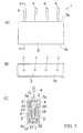
Figs. 1 are views illustrating one embodiment of a capacitor element manufacturing jig according to the invention, in whichFig. 1(A) is a front view andFig. 1(B) is a rear view. -
Fig. 2 is a left side view of the capacitor element manufacturing jig ofFig. 1 . -
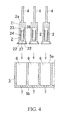
Figs. 3 are views in which one embodiment of a gang socket of the invention is enlarged, in whichFig. 3(A) is a front view,Fig. 3(B) is a bottom plan view, andFig. 3(C) is a cross sectional view along the Y-Y line ofFig. 3(A) . -
Fig. 4 is a cross sectional view in which a socket main units and an insulator part are separated. -
Fig. 5 is a perspective view illustrating an insulator part. -
Figs. 6(A), 6(B), and 6(C) are all cross sectional views illustrating another embodiment of the gang socket of the invention. -
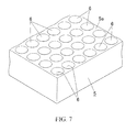
Fig. 7 is a perspective view illustrating another example of the insulator part. -
Fig. 8 is an outline view illustrating a method for manufacturing a capacitor element using a capacitor element manufacturing jig of the invention. -
Fig. 9 is a cross sectional view illustrating a connection manner of a socket and an anode body inFig. 8 . -
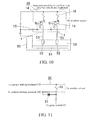
Fig. 10 is a schematic view illustrating a method for manufacturing a capacitor element of the invention as an electrical circuit (As the circuit in the capacitor element manufacturing jig, only two circuits are illustrated). -
Fig. 11 is a circuit diagram illustrating another example of an electrical connection circuit in a circuit board of the capacitor element manufacturing jig. -
Fig. 12 is a partial cross sectional view illustrating one embodiment of a capacitor element manufactured by a manufacturing method according to the invention. - One embodiment of a
gang socket 1 according to the invention is illustrated inFig. 3 . Thegang socket 1 has a plurality of conductive socketmain units 2 and an insulator part 5 (Figs. 3 to 5 ). Preferably, in order to facilitate attachment to and detachment from aconnection portion 88 described later, onelead wire portion 4 is extended from anupper surface 2a of each of the socketmain units 2. In this embodiment, the plurality of socketmain units 2 are connected in one row through theinsulator part 5, whereby aparallel gang socket 1 is constituted (Figs. 3 to 5 ). - The socket
main unit 2 is a member having a function as an electrical connection terminal for achieving electrical connection with ananode body 52 and the like and is constituted of conductive materials, such as metal materials, in order to achieve electrical continuity. Metals constituting the socketmain units 2 are not particularly limited and preferably contains metal (including alloy) containing at least one metal selected from the group consisting of copper, iron, silver, and aluminum as the main component (containing in a proportion of 50% by mass or more). On the surface of the socketmain units 2, at least one layer of known plating, such as tin plating, solder plating, nickel plating, gold plating, silver plating, and copper plating, may be provided. - In this embodiment, the socket
main units 2 each have apillar portion 21 and aninclined surface portion 22 downwardly extended from a peripheral portion of the bottom surface of thepillar portion 21 in such a manner as to outwardly extend (Figs. 3 and4 ) and thepillar portion 21 and theinclined surface portion 22 are constituted of conductive materials, such as metal materials. A leadwire insertion opening 37 is formed at the central portion of the bottom surface of the pillar portion 21 (Figs. 3 and4 ).Hollow portions 23 are provided in each of thepillar portions 21. Thehollow portions 23 are connected to the leadwire insertion openings 37. Ametal spring member 24 is continuously connected to the inner circumferential surface of thehollow portions 23. A leadwire insertion hole 38 is formed while being surrounded by themetal spring member 24. The lead wire insertion holes 38 are connected to the space of the leadwire insertion openings 37. The socketmain unit 2 and theanode body 52 are electrically connected by inserting and disposing alead wire 53 and the like of theanode body 52 in the leadwire insertion hole 38 in a contact state. - The socket
main units 2 are connected to anelectrical circuit 30 described later through aconnection portion 88 described later. The connection is not particularly limited insofar as the connection is electrically connectable and the following connection manner is mentioned, for example. - The
lead wire portion 4 is extended from the central portion of anupper surface 2a (upper surface of the pillar portion 21) of the socket main units 2 (Figs. 3 and4 ). Thelead wire portion 4 is constituted of conductive materials, such as metal materials. More specifically, thelead wire portion 4 is integrally formed with the socketmain unit 2 and is electrically connected to the socketmain unit 2. As metals constituting thelead wire portion 4, the same metals as those mentioned as metals constituting the socketmain units 2 are mentioned. Thelead wire portion 4 is usually constituted of the same metal as the metal constituting the socketmain units 2. - At least a
lower surface 5b, preferably thelower surface 5b and the side surface, of theinsulator part 5 is constituted of materials having corrosion resistance. Furthermore, theinsulator part 5 is preferably constituted of materials also having heat resistance. In theinsulator part 5, a plurality of receivingunits 6 each having a shape capable of accommodating at least part of the socket main units 2 (for example, a shape having a pillar-shaped concave portion) are provided in one row on anupper surface 5a and the like and a plurality ofsmall holes 7 are formed in alower surface 5b (Figs. 3 to 5 ). More specifically, onesmall hole 7 connecting to the bottom surface is formed immediately under the bottom surface of each of the receivingunits 6 in thelower surface 5b of the insulator part 5 (Figs. 3 and4 ). In the embodiment described above, the plurality of receivingunits 6 are disposed in one row in the insulator part 5 (Fig. 5 ) but the invention is not particularly limited to such an aspect. For example, as illustrated inFig. 7 , a configuration in which a large number of receivingunits 6 are provided in a plurality of rows (configuration in which a plurality of lines are disposed in the transverse direction and a plurality of rows are disposed in the longitudinal direction) may be adopted. - The materials constituting the
insulator part 5 are preferably materials having corrosion resistance and more preferably materials having heat resistance and corrosion resistance. As a specific example of the materials having corrosion resistance, a material, such as synthetic resin, ceramics, glass, or stainless steel, is suitably used, for example. The materials constituting theinsulator part 5 are more preferably materials having heat resistance and corrosion resistance and materials, such as ceramics, glass, and stainless steel, are mentioned. When using stainless steel, it is necessary to constitute the same in such a manner as to achieve insulation with themetal spring member 24. - The synthetic resin material is not particularly limited and, for example, hard resin, such as epoxy resin, phenol resin, imide resin, carbonate resin, amide resin, amide imide resin, ester resin, and phenylene sulfide resin, and the like are mentioned.
- The ceramic material is not particularly limited and, for example, alumina, zirconia, titania, and the like are mentioned.
- The glass material is not particularly limited and, for example, borosilicate glass and the like are mentioned.
- When a transparent material is used as the material constituting the
insulator part 5, the occurrence of corrosion of the socketmain units 2 and the corrosion level can be easily visually confirmed. - In general, the
lead wire 53 of the anode body has a transverse cross sectional shape of a circle having an outer diameter of 0.1 mm to 0.5 mm or an approximately rectangle having a side length of 0.1 mm to 0.5 mm. Thus, the shape of thesmall holes 7 as viewed in plan from the lower side is preferably a circular shape having an inner diameter of larger than 0.1 mm and 0.55 mm or lower or a rectangular shape having one side of larger than 0.1 mm and 0.55 mm or lower. More specifically, as the shape of thesmall holes 7 as viewed in plan from the lower side, thesmall holes 7 are preferably larger than a 0.1 mm diameter circle and are equal to or smaller than a 0.55 mm square. - Or, as the shape of the
small holes 7 as viewed in plan from the lower side, thesmall holes 7 are preferably set, in accordance with the transverse cross sectional shape of thelead wire 53 of the anode body to be inserted thereto, to be larger than the transverse cross sectional shape and is equal to or smaller than a similar figure in which the transverse cross sectional shape is enlarged by 1.1 times. For example, when the transverse cross sectional shape of thelead wire 53 of the anode body has a circular shape, the diameter of thesmall holes 7 are preferably set to be larger than the outer diameter of thelead wire 53 of the anode body to be inserted thereto and to be equal to or smaller than a diameter 1.1 times larger than the outer diameter. More specifically, when the outer diameter of thelead wire 53 is 0.29 mm, the diameter of thesmall holes 7 is preferably set to 0.30 mm to 0.31 mm. - By setting the size in the range mentioned above, the corrosion of the socket main units 2 (particularly insertion openings) can sufficiently be prevented. The
small holes 7 may have a tapered portion. For example, thesmall holes 7 may be holes of an approximately pillar shape as illustrated inFig. 3 and, in addition thereto, may be a hole of a truncated cone shape which downwardly extends as illustrated inFig. 6(C) . - In order to suppress the corrosion of the socket
main units 2, the depth of thesmall holes 7 may be larger.
However, in order to reduce the length of thelead wire 53 of the anode body to reduce the cost of materials, the depth may be smaller. Thus, the range of the depth of thesmall holes 7 is preferably 0.2 mm to 8 mm, more preferably 0.5 mm to 6 mm, and still more preferably 1 mm to 3 mm. When the transverse cross sectional shape of the small holes 7 (When the transverse cross sectional shape is uniform, the transverse cross sectional shape is in agreement with the shape of thesmall holes 7 as viewed in plan from the lower side.) has a portion exceeding all the dimension ranges of the shape of thesmall holes 7 as viewed in plan from the lower side. e.g., when thesmall holes 7 have a tapered portion, it is more preferable to set the depth of thesmall holes 7 not including the portion to be equal to or lower than the lower limit of the depth range mentioned above. - Thus, the entire socket
main units 2 are accommodated in the receivingunit 6 of theinsulator part 5 and also agap 9 between the accommodated socketmain units 2 and theinsulator part 5 is filled up with afiller 3, such as a low melting glass (for example, glass whose melting point is 600°C), so that the socketmain units 2 and the receivingunit 6 are welded or the like, whereby the socketmain units 2 are secured in the receivingunits 6 of the insulator part 5 (Fig. 3 ). In the secured state, the leadwire insertion openings 37 of the socketmain units 2 and thesmall holes 7 of theinsulator part 5 are connected to each other (Fig. 3 ). Anupper surface 3a of theenclosed glass 3 is located at a position lower than theupper surface 5a of the insulator part 5 (Fig. 3 ). Anupper surface 2a of the socketmain units 2 is located at a position lower than theupper surface 5a of the insulator part 5 (Fig. 3 ). - When the
gang socket 1 according to the configuration described above is attached to theconnection portion 88 attached to thecircuit board 11, for example, as described later, the vertical position (attachment height of thegang socket 1 of the invention) of the attachment of thegang socket 1 can be accurately determined by attaching in such a manner that theupper surface 5a of theinsulator part 5 abuts on the lower surface of the connection portion 88 (Figs. 1 and2 ). - The heat resistance temperature of the
gang socket 1 according to the configuration described above is dependent on the low melting glass. Thegang socket 1 is usually used at a temperature equal to or lower than the deformation temperature of the used low melting glass. - Next, another embodiment of the
gang socket 1 according to the invention is illustrated inFigs. 6 . In the configuration illustrated inFig. 6(A) , the entire socketmain units 2 are accommodated in the receivingunit 6 of theinsulator part 5 and also only an upper portion in thegap 9 between the accommodated socketmain units 2 and theinsulator part 5 is filled with theglass material 3, such as low melting glass, whereby the socketmain units 2 are secured into the receivingunits 6 of theinsulator part 5. In the secured state, the leadwire insertion openings 37 of the socketmain units 2 and thesmall holes 7 of theinsulator part 5 are connected to each other. Theupper surface 3a of theenclosed glass 3 is located at a position lower than theupper surface 5a of theinsulator part 5. Theupper surface 2a of the socketmain units 2 is located at a position lower than theupper surface 5a of theinsulator part 5. Thus, when thegang socket 1 illustrated inFig. 6(A) is attached to theconnection portion 88 attached to thecircuit board 11, for example, as described later, the vertical position (attachment height of thegang socket 1 of the invention) of the attachment of thegang socket 1 can be accurately determined by attaching in such a manner that theupper surface 5a of theinsulator part 5 abuts on the lower surface of theconnection portion 88. - In the configuration illustrated in
Fig. 6(B) , a part of the socketmain units 2 is accommodated in the receivingunit 6 of theinsulator part 5 and also thegap 9 between the accommodated socketmain units 2 and theinsulator part 5 is filled with theglass material 3, such as low melting glass, whereby the socketmain units 2 are secured into the receivingunit 6 of theinsulator part 5. In the secured state, the leadwire insertion openings 37 of the socketmain units 2 and thesmall holes 7 of theinsulator part 5 are connected to each other. Theupper surface 3a of theenclosed glass 3 is located at a position lower than theupper surface 2a of the socketmain units 2. Theupper surface 2a of the socketmain units 2 is located at a position higher than theupper surface 5a of theinsulator part 5. Thus, when thegang socket 1 illustrated inFig. 6(B) is attached to theconnection portion 88 attached to thecircuit board 11, for example, as described later, the vertical position (attachment height of thegang socket 1 of the invention) of the attachment of thegang socket 1 can be accurately determined by attaching in such a manner that theupper surface 2a of the socketmain units 2 abuts on the lower surface of theconnection portion 88. - In the configuration illustrated in
Fig. 6(C) , the entire socketmain units 2 are accommodated in the receivingunit 6 of theinsulator part 5. Thegap 9 is not present between the accommodated socketmain units 2 and theinsulator part 5 except for an upper region and thegap 9 is present in the upper region between the socketmain units 2 and theinsulator part 5. By filling thegap 9 with theglass material 3, such as low melting glass, the socketmain units 2 are secured into the receivingunit 6 of theinsulator part 5. In the secured state, the leadwire insertion openings 37 of the socketmain units 2 and thesmall holes 7 of theinsulator part 5 are connected to each other. Theupper surface 2a of the socketmain units 2 is located at a position lower than theupper surface 5a of theinsulator part 5. Theglass material 3, such as low melting glass, is enclosed also in theupper surface 2a of the socketmain units 2 and theupper surface 3a of theenclosed glass 3 is located at a position lower than theupper surface 5a of theinsulator part 5. Thus, when thegang socket 1 illustrated inFig. 6(C) is attached to theconnection portion 88 attached to thecircuit board 11, for example, as described later, the vertical position (attachment height of thegang socket 1 of the invention) of the attachment of thegang socket 1 can be accurately determined by attaching in such a manner that theupper surface 5a of theinsulator part 5 abuts on the lower surface of theconnection portion 88. - Next, one embodiment of a capacitor
element manufacturing jig 10 according to the invention is illustrated inFigs. 1 and2 . The capacitorelement manufacturing jig 10 is constituted using thegang socket 1 of the invention described above. The capacitorelement manufacturing jig 10 has thecircuit board 11 and thegang socket 1. - As the
circuit board 11, an insulating board is used. The material of the insulating substrate is not particularly limited and, for example, glass epoxy resin, imide resin, ceramics, and the like are mentioned. - On the surface of the
circuit board 11, anelectrical circuit 30 having a pair ofelectrical connection terminals Fig. 1 . Theelectrical circuit 30 has a circuit which limits a current (for example, circuits ofFigs. 10 and 11 and the like) and supplies a current independently in eachanode body 52 through thegang socket 1 of the invention and thelead wire 53 connected thereto. - Thus, the highest current value flowing into each
anode body 52 becomes a current limit value of the circuit. The circuit which limits a current is preferably a constant current circuit (for example,Fig. 10 ) in order to reduce the deviation of a capacitor to be obtained as much as possible. Theelectrical circuit 30 is more preferably a circuit which further limits a voltage to be applied to eachanode body 52. Even when a relatively high current is supplied, the greatest voltage value to be applied to theanode body 52 is limited. Thus, the treatment time of the chemical conversion or the semiconductor layer formation can be shortened. - With respect to the pair of
electrical connection terminal terminal 14 is provided at one end portion in the longitudinal direction of thecircuit board 11 and theother terminal 15 is provided at the other end portion in the longitudinal direction of thecircuit board 11. One electrical connection terminal is a current limitingterminal 14, and the current limit value is set based on the voltage supplied to the terminal 14. For example, in the case of the circuit ofFig. 10 , the current limit value can set based on a potential difference between the current limitingterminal 14 and avoltage limiting terminal 15 described later. In the case of the circuit ofFig. 11 , the current limit value can set based on a potential difference between the current limitingterminal 14 and acathode plate 51. - The other electrical connection terminal is a
voltage limiting terminal 15. The highest voltage value to be applied to eachanode body 52 is limited based on the voltage supplied to the terminal 15. For example, in the case of the circuits ofFigs. 10 and 11 , the highest voltage value can be set based on a potential difference between thevoltage limiting terminal 15 and thecathode plate 51. InFigs. 10 and 11 , 18 denotes a resistor, 19 denotes a transistor, and 31 denotes a diode. - The
gang socket 1 is attached to the lower end portion of thecircuit board 11. More specifically, as illustrated inFigs. 1 and2 , theconnection portion 88 of thegang socket 1 is secured to thecircuit board 11, alead wire portion 84 upwardly extended from eachconnection portion 81 is bent at an angle of about 90° in a curved manner, and then the top end portion of thelead wire portion 84 is inserted into each penetration hole provided in the lower portion of thecircuit board 11 and is attached to thecircuit board 11 with a solder 20 (Fig. 2 ). - In
Figs. 1 and2 , a general gang socket (sometimes referred to as a "firstrow gang socket 88" in order to distinguish the gang socket from the gang socket 1) capable of connecting thegang socket 1 is used as theconnection portion 88. - Then, the
lead wire portion 4 of each of the socketmain units 2 of thegang socket 1 of the invention is inserted and connected to the insertion opening in the bottom surface of each of theconnection portions 81 attached to thecircuit board 11, whereby thegang socket 1 is attached to the lower end portion of the circuit board 11 (Figs. 1 ,2 , and9 ). The gang socket 1 (parallel gang socket 1 in which the plurality of socketmain units 2 are connected in one row through the insulator part 5) is attached to thecircuit board 11 in such an aspect, whereby the capacitorelement manufacturing jig 10 of the invention is constituted. In theconnection portion 88 illustrated inFig. 2 , 82 denotes a conductive socket main unit and 85 denotes an insulator part formed with resin. - In the invention, an electrical connection circuit of the
circuit board 11 of the capacitorelement manufacturing jig 10 is not particularly limited to one having the configuration illustrated inFig. 10 and may have a circuit configuration illustrated inFig. 11 , for example. - Next, a method for manufacturing a capacitor element using the capacitor
element manufacturing jig 10 described above is described.Fig. 8 illustrates one example of a method for manufacturing a capacitor element in an outline view.Fig. 10 is a schematic view illustrating a method for manufacturing a capacitor element as an electrical circuit. - First, a
treatment container 50 in which atreatment liquid 59 is put is prepared. As thetreatment liquid 59, a chemical conversion treatment liquid for forming thedielectric layer 54, a semiconductor layer forming liquid for forming asemiconductor layer 55, and the like are mentioned. - Separately, the
anode body 52 having thelead wire 53 is connected to thegang socket 1 of the capacitorelement manufacturing jig 10. More specifically, by inserting thelead wire 53 of theanode body 52 into the leadwire insertion hole 38 through the leadwire insertion opening 37 of thegang socket 1 of the capacitorelement manufacturing jig 10, theanode body 52 is electrically connected to the gang socket 1 (Fig. 9 ). Since the top end side of thelead wire 53 contacts themetal spring member 24 in thehollow portions 23 of the socketmain units 2, thegang socket 1 and theanode body 52 are electrically connected. - Subsequently, the capacitor
element manufacturing jig 10 in which theanode body 52 is set is disposed at the upper position of thetreatment container 50, thejig 10 is lowered (or thetreatment container 50 is raised) until at least one part (usually entire) of theanode body 52 is immersed in thetreatment liquid 59, and then thejig 10 is secured at the height (Fig. 8 ). - In the immersed state of the
anode body 52, energization is performed while using theanode body 52 as an anode and using thecathode plate 51 disposed in thetreatment liquid 59 as a cathode (Figs. 8 and10 ). When the chemical conversion treatment liquid is used as afirst treatment liquid 59, the dielectric layer 54 (Fig. 12 ) can be formed on the surface of theanode body 52 by the energization (dielectric layer formation process). - Subsequently, the
anode body 52 having thedielectric layer 54 on the surface is washed with water and dried as required, the semiconductorlayer forming liquid 59 is newly put into anothertreatment container 50 different from the treatment container above, thejig 10 is lowered until at least one part (usually entire) of theanode body 52 is immersed in the semiconductorlayer forming liquid 59 in the same manner as above, and then thejig 10 is secured at the height. Then, when energization is performed while using theanode body 52 as an anode and using thecathode plate 51 disposed in the semiconductorlayer forming liquid 59 as a cathode, more specifically, when energization is performed using the semiconductor layer forming liquid as asecond treatment liquid 59, thesemiconductor layer 55 can be formed on the surface of thedielectric layer 54 on the surface of the anode body 52 (semiconductor layer formation process). Thus, acapacitor element 56 in which thedielectric layer 54 is laminated on the surface of theanode body 52 and thesemiconductor layer 55 is further laminated on the surface of thedielectric layer 54 can be manufactured (Fig. 12 ). - In the method for manufacturing a capacitor element according to the invention, for example, between the dielectric layer formation process and the semiconductor layer formation process and/or after the semiconductor layer formation process, the
gang socket 1 to which theanode bodies 52 are connected is removed from theconnection portion 88 of thecircuit board 11 of thecapacitor manufacturing jig 10, and theanode bodies 52 connected to thegang socket 1 is heat treated (heat treatment process). Since thegang socket 1 is detachably attached to theconnection portion 88 electrically connected to thecircuit board 11, the gang socket 1 (in the state where theanode bodies 52 are connected) can be removed from theconnection portion 88, and only the gang socket 1 (in the state where theanode bodies 52 are connected) can be heat treated (The application of the heat treatment to thecircuit board 11 and the like can be avoided.). - The heat treatment is performed for the purpose of mainly increasing the reliability of the capacitor, and the timing for the heat treatment varies depending on the intended use. The heating temperature of the heat treatment performed between the dielectric layer formation process and the semiconductor layer formation process is usually 200°C to 500°C. The heating temperature of the heat treatment performed between the semiconductor layer formation process and a carbon paste formation process is usually 150°C to 300°C. The heating temperature of the heat treatment performed between the carbon paste formation process and a silver paste formation process is usually 150°C to 300°C.
- The atmosphere in the heat treatment is preferably an inactive gas atmosphere, such as argon gas, or a reduced pressure atmosphere. Since nitrogen reacts with anode body materials, such as niobium, even at a temperature of about 300°C, nitrogen is not used as the inactive gas.
- In order to further perform treatment after the heat treatment, the gang socket 1 (in the state where the
anode bodies 52 are connected) may be attached to theconnection portion 88 again after the heat treatment, and electrically connected. - In the heat treatment process above, a reason why the heat treatment is not performed in a state where only the
anode bodies 52 are removed and the heat treatment is performed to thegang socket 1 to which theanode bodies 52 are connected after thegang socket 1 to which theanode bodies 52 are connected is removed from theconnection portion 88 of thecircuit board 11 resides in that when only theanode bodies 52 are removed from thegang socket 1, there is a possibility of damaging thedielectric layer 54 and thesemiconductor layer 55 already formed on theanode body 52. This is also because when requiring further treatment after the heat treatment in the case where only theanode bodies 52 are removed from thegang socket 1, theanode bodies 52 are required to be attached again to thegang socket 1, and there is a possibility of similarly damaging thedielectric layer 54 and thesemiconductor layer 55 already formed on theanode body 52 in this case. - The size of the
gang socket 1 is not particularly limited and may be adjusted to the size according to the arrangement of the capacitor element when immersed in thetreatment liquid 59, the size which allows easy handling according to a device which conveys thegang socket 1, and the like. - The
anode body 52 is not particularly limited and at least one anode body selected from the group consisting of valve action metals and conductive oxides of valve action metals, can be mentioned, for example. As a specific example thereof, aluminum, tantalum, niobium, titanium, zirconium, niobium monoxide, zirconium monoxide, and the like are mentioned. Or, a laminate in which the anode body is laminated on the surface of a base substance may be acceptable. As an example of the laminate in which the anode body is laminated on a surface layer, a laminate in which the anode body is laminated on a base substance, such as paper, insulating polymer, and glass, and the like are mentioned. - The shape of the
anode body 52 is not particularly limited and a foil shape, a plate shape, a cylindrical shape, a rectangular parallelepiped shape, and the like are mentioned. - The chemical
conversion treatment liquid 59 is not particularly limited and, for example, a liquid in which known electrolytes, such as organic acids or salts thereof (for example, adipic acid, acetic acid, ammonium adipate, benzoic acid, and the like) or inorganic acids or salts thereof (for example, phosphoric acid, silicic acid, ammonium phosphate, ammonium silicate, sulfuric acid, ammonium sulfate, and the like) is dissolved or suspended and the like are mentioned. By performing the energization using such a chemical conversion treatment liquid, thedielectric layer 54 containing an insulating metal oxide, such as Ta2O5, Al2O3, Zr2O3, and Nb2O5, can be formed on the surface of theanode body 52. - The dielectric layer formation process using such a chemical conversion treatment liquid may be omitted, and the
anode body 52 on the surface of which thedielectric layer 54 is already provided may be subjected to the semiconductor layer formation process. As thedielectric layer 54 on the surface, a dielectric layer containing at least one selected from insulating oxides as the main component and a dielectric layer known in the fields of a ceramic capacitor and a film capacitor are mentioned. - The semiconductor
layer forming liquid 59 is not particularly limited insofar as the solution can form a semiconductor by energization. For example, a solution and the like containing aniline, thiophene, pyrrole, methylpyrrole, substituted derivatives thereof (for example, 3,4-ethylenedioxythiophene and the like), and the like, are mentioned. A dopant may be further added to the semiconductorlayer forming liquid 59. The dopant is not particularly limited and, for example, known dopants, such as aryl sulfonic acid or a salt thereof, alkyl sulfonic acid or a salt thereof, various polymeric sulfonic acids or salts thereof, and the like are mentioned. By performing the energization using such a semiconductorlayer forming liquid 59, thesemiconductor layer 55 containing, for example, conductive polymers (for example, polyaniline, polythiophene, polypyrrole, polymethylpyrrole, and the like) can be formed on the surface of thedielectric layer 54 on the surface of theanode body 52. - In the invention, on the
semiconductor layer 55 of thecapacitor element 56 obtained by the manufacturing method described above, an electrode layer may be provided in order to improve electrical contact with an external lead-out terminal (for example, lead frame) of a capacitor. - The electrode layer can be formed by, for example, solidification of a conductive paste, plating, metal vapor deposition, formation of a heat-resistant conductive resin film, and the like. As the conductive paste, silver paste, copper paste, aluminum paste, carbon paste, nickel paste, and the like are preferable.
- To each of the
anode body 52 and thesemiconductor layer 55 of thecapacitor element 56 thus obtained, an electrode terminal is electrically connected (for example, thelead wire 53 is welded to one electrode terminal and the electrode layer (semiconductor layer) 55 is attached to the other electrode terminal with silver paste or the like), and then sealing is performed while leaving a part of the electrode terminals, whereby a capacitor is obtained. - The sealing method is not particularly limited and resin mold sheathing, resin case sheathing, metal case sheathing, sheathing by dipping of resin, sheathing by a laminate film, and the like are mentioned, for example. Among the above, since a reduction in size and a reduction in cost can be easily achieved, resin mold sheathing is preferable.
- Next, specific Examples of the invention are described but the invention is not particularly limited to the Examples.
- By granulating niobium primary powder (average particle diameter of 0.32 µm) obtained by pulverizing a niobium (Nb) ingot utilizing hydrogen brittleness, niobium powder having an average particle diameter of 124 µm was obtained (The niobium powder has a naturally-oxidized surface and contains 8900 ppm of oxygen.). Next, the obtained niobium powder was allowed to stand in a 450°C nitrogen atmosphere, and further allowed to stand in a 700°C argon atmosphere, whereby partially-nitrided niobium powder (CV value: 290000 µF·V/g) having a nitride amount of 8000 ppm was obtained. The partially-nitrided niobium powder was molded with a niobium wire (lead wire) having a diameter of 0.29 mm, and then sintered at 1270°C, whereby a sintered body (anode body) 52 having a rectangular parallelepiped shape of 2.3 mm in length × 1.7 mm in width × 1.0 mm in thickness was produced. The
niobium lead wire 53 is integrally molded in such a manner that thelead wire 53 is buried in thesintered body 52 at a position inwardly positioned from the surface of 1.7 mm × 1.0 mm of thesintered body 52 by 1.3 mm and outwardly projected by 10 mm from the center of the surface. - The
parallel gang socket 1 having the configuration illustrated inFigs. 3 to 5 was produced. Theinsulator part 5 contains an alumina sintered body obtained by sintering alumina powder. The diameter of thesmall holes 7 is 0.306 mm ± 0.012 mm and the depth of thesmall holes 7 is 1.6 mm. On theupper surface 5a of theinsulator part 5, 64 receivingunits 6 are formed at equal intervals (2.54 mm pitch) (Fig. 5 ). One small hole 7 (64 holes in total) connecting to the bottom surface is formed immediately under the bottom surface of each of the receivingunits 6 in thelower surface 5b of the insulator part 5 (Figs. 3 and4 ). Each of the 64 socketmain units 2 was accommodated in each of the receivingunits 6 of theinsulator part 5 and also thegap 9 between each of the accommodated socketmain units 2 and theinsulator part 5 was filled with a low melting glass (glass whose melting point is 400°C) powder. Then, the powder was melted for sticking them to thereby fix each of the socketmain units 2 into each of the receivingunits 6 of theinsulator part 5, whereby theparallel gang socket 1 was obtained (Fig. 3 ). In thegang socket 1, the leadwire insertion openings 37 of the socketmain units 2 and thesmall holes 7 of theinsulator part 5 are connected to each other (Fig. 3 ). Theupper surface 3a of theenclosed glass 3 is located at a position lower than theupper surface 5a of theinsulator part 5 and theupper surface 2a of the socketmain units 2 is located at a position lower than theupper surface 5a of the insulator part 5 (Fig. 3 ). - A copper-clad glass epoxy board (circuit board) 11 of 194.0 mm in length × 33.0 mm in width × 1.6 mm in thickness was prepared (
Fig. 1 ). The copper-cladglass epoxy board 11 is provided with 10 mm × 8 mm cut-outportions terminal portions portions Fig. 1(A) ). The current limitingterminal 14 is provided at the upper region of one cut-outportion 12 and thevoltage limiting terminal 15 is provided at the upper region of the other cut-out portion 13 (Fig. 1(A) ). The electrical terminal portion 14 (Fig. 1(A) ) at the front surface side is electrically connected to the electrical terminal portion 14 (Fig. 1 (B) ) of the same area at the back surface side through a throughhole 16 in theterminal portion 14. The electrical terminal portion 15 (Fig. 1(A) ) at the front surface side is electrically connected to the electrical terminal portion 15 (Fig. 1(B) ) of the same area at the back surface side through a throughhole 16 in theterminal portion 15. - On the copper-clad
glass epoxy board 11, the circuit ofFig. 10 , i.e., 64resistors 18 of 20 kΩ (1% of error) 18, 64 transistors (2SA2154GR) 19, and the first row gang socket 88 (manufactured by Preci-dip corporation, "PCD receptacle 399 series round pin DIP socket", 2.54 mm pitch, 64 pin gang socket) 88 as theconnection portion 88 at only one surface (front surface) are mounted (Figs. 1 and2 ). - As illustrated in
FIG. 2 , thelead wire 84 of each of theconnection portions 81 was upwardly extended from the upper surface of the socketmain units 82, bent toward theboard 11 at an angle of about 90° in a curved manner, inserted into each of 64 holes formed in the lower portion of theboard 11, and then attached to thecircuit board 11 with asolder 20. - Each
lead wire 4 of thegang socket 1 of the invention was inserted into and connected to the lead wire insertion opening formed in a dented manner in the bottom surface of the firstrow gang socket 88, and thegang socket 1 of the invention was detachably connected to the lower portion of the firstrow gang socket 88 to thereby form a two-stage structure. Thus, a solid electrolytic capacitorelement manufacturing jig 10 in which thegang socket 1 was detachably attached to the copper-clad glass epoxy board (circuit board) 11 was obtained (Figs. 1 and2 ). A secondrow gang socket 1 is used as ananode body 52 connection terminal. - As illustrated in
Fig. 10 , oneresistor 18 and an emitter E of onetransistor 19 mounted on thecircuit board 11 are connected to each other and a collector C of thetransistor 19 is electrically connected to one socketmain units 2 of thegang socket 1. The other side of theresistor 18 is connected to the current limitingterminal 14. A base B of thetransistor 19 is connected to thevoltage limiting terminal 15. - A
niobium lead wire 53 of the anode body (conductive sintered body) 52 was inserted into each leadwire insertion hole 38 of thegang socket 1 of the solid electrolytic capacitorelement manufacturing jig 10 to be electrically connected thereto (FIGS. 8 and9 ). The heights of the 64 anode bodies (conductive sintered body) 52 were made uniform and the directions were also made uniform as illustrated inFig. 8 . Ten capacitorelement producing jigs 10 each having sixteen fouranode bodies 52 connected thereto as described above were prepared, and attached to a holding frame in which the jigs are arranged in parallel in such a manner that theconnected anode bodies 52 were downwardly suspended. The holding frame has a socket into which theelectrical connection terminals element manufacturing jig 10 are inserted. The holding frame was disposed at an upper position of a metallic (stainless steel)treatment container 50 containing a 1% by mass aqueous phosphoric acid solution (chemical conversion treatment liquid) 59 (FIG. 8 ). The 10 capacitor element manufacturing jigs 10 were attached in parallel to the holding frame at intervals of 8 mm. Themetallic treatment container 50 also functions as thecathode plate 51. - The holding frame was operated, so that the
jigs 10 were lowered in such a manner that theentire anode bodies 52 and a 5 mm length portion of the lower end portion of thelead wire 53 were immersed in thetreatment liquid 59, and secured at the height. In this immersed state, a voltage was applied between thevoltage limiting terminal 15 and the cathode plate 51 (containing the metallic treatment container 50) in such a manner that the voltage limiting value (chemical conversion voltage) became 8.3 V and a voltage was applied between the current limitingterminal 14 and thevoltage limiting terminal 15 in such a manner that the current limiting value became 2.1 mA for energization. In the state where the temperature of the chemicalconversion treatment liquid 59 was maintained at 65°C, anodization was performed for 8 hours. Thus, thedielectric layer 54 was formed on the pores and the outer surface of the conductivesintered body 52 and the surface of a part (5 mm length portion) of the lead wire. Under the anodization, for 4 hours of the second half from the passage of 4 hours to the passage of 8 hours, the current limit value was continuously reduced at a rate of 0.5 mA per hour (dielectric layer formation process). - The
anode body 52 having thedielectric layer 54 on the surface was washed with water and dried, and then immersed in a 20% by mass ethylene dioxythiophene ethanol solution. Separately, the semiconductor layer forming liquid 59 (a solution in which 0.4% by mass of ethylene dioxythiophene and 0.6% by mass of anthraquinone sulfonic acid were compounded in a mixed solvent containing 30 parts by mass of water and 70 parts by mass of ethylene glycol) was put into anothertreatment container 50 different from thetreatment container 50 above, and then thejig 10 was lowered in such a manner that theentire anode bodies 52 each having thedielectric layer 54 on the surface and a 5 mm length portion of the lower end portion of thelead wire 53 were immersed in the semiconductorlayer forming liquid 59, and secured at the height. In the immersed state, electrolytic polymerization was performed at 20°C for 1 hour. - In the electrolytic polymerization, the voltage limit value was set to 10 V and the current limit value was set to 44 µA for the first 15 minutes. For the next 15 minutes, the voltage limit value was set to 10 V and the current limit value was set to 82 µA. For the last 30 minutes, the voltage limit value was set to 10 V and the current limit value was set to 101 µA.
- By performing the 1 hour
electrolytic polymerization 6 times (electrolytic polymerization for 6 hours in total), thesemiconductor layer 55 containing a conductive polymer was formed on the surface of thedielectric layer 54 of theanode body 52 on the surface of which thedielectric layer 54 was formed (semiconductor layer formation process). - Subsequently, by performing re-chemical conversion, the
dielectric layer 54 was repaired. The re-chemical conversion was performed at a controlled voltage of 6.3V and a controlled current of 0.1 mA for 15 minutes using the same solution as that of the anodization (First re-chemical conversion treatment process). - Next, a carbon paste (manufactured by Acheson, "Electrodag PR-406") was applied to the surface of the
semiconductor layer 55, and then dried at 125°C (carbon paste application process). - Next, the gang socket 1 (in the state where the
anode bodies 52 on each of which thedielectric layer 54, thesemiconductor layer 55, and the carbon paste were laminated were connected) was removed from the firstrow gang socket 88 of the capacitorelement manufacturing jig 10, and then thegang socket 1 was allowed to stand at 190°C for 30 minutes under reduced pressure of a gauge pressure of minus 99 KPa to be heat treated (first heat treatment process). After returning to room temperature, 1% oxygen containing nitrogen gas was supplied into a pressure reducing device in such a manner that the gauge pressure became minus 80 KPa, and then it was allowed to stand for 30 minutes. Thereafter, the pressure was returned to reduced pressure of a gauge pressure of minus 99 KPa. The sequence of operations of supplying oxygen containing nitrogen gas and then returning the pressure to reduced pressure of a gauge pressure of minus 99 KPa was further repeated 8 times, air was supplied into the pressure reducing device, and then the gang socket 1 (in the state where theanode bodies 52 on each of which thedielectric layer 54, thesemiconductor layer 55, and the carbon paste were laminated were connected) was taken out from the pressure reducing device. - Next, each
lead wire 4 of the gang socket 1 (in the state where theanode bodies 52 on each of which thedielectric layer 54 and thesemiconductor layer 55 were laminated were connected) was inserted into each lead wire insertion opening in the bottom surface of the firstrow gang socket 88 of the capacitorelement manufacturing jig 10 again, and then connected (electrically connected). Ten capacitorelement manufacturing jigs 10 to which thegang socket 1 was attached as described above were prepared, attached to a holding frame in the same manner as above, and then re-chemical conversion was performed under the same conditions as those of the first re-chemical conversion after the polymerization (second re-chemical conversion treatment process). - Next, the
anode body 52 on which thedielectric layer 54, thesemiconductor layer 55, and the carbon paste were laminated was washed with water and then dried. Thereafter, a silver paste was laminated on the surface of the carbon paste layer to thereby form the anode body layer (silver paste lamination process), thereby obtaining thecapacitor element 56. - Next, the
capacitor element 56 was placed on a lead frame, an anode lead wire (semiconductor side) of the capacitor element was connected to an anode terminal of the lead frame, theanode body 52 of the capacitor element was connected to a cathode terminal of the lead frame, and then transfer sealing and aging were performed, thereby producing 640 niobium solid electrolytic capacitors having a size of 3.5 mm × 2.8 mm × 1.8 mm, a rating of 2.5 V, and a capacity of 330 µF. - 500 capacitors of the produced 640 niobium solid electrolytic capacitors were soldered to a mounting board for the test by a reflow furnace. The reflow conditions were as follows; 30 seconds at a preheating of 225°C and 3 seconds at a peak temperature of 250°C. The capacitor thus mounted was subjected to a load test at a temperature of 110°C and at an applied voltage of 2.5 V for 2000 hours using a load test device. Thereafter, the leak current value at 2.5 V of the niobium solid electrolytic capacitors was actually measured. As a result, the values of all the 500 niobium solid electrolytic capacitors were within 0.1 CVµA. Herein, 0.1 CV is a numerical value obtained by multiplying the product of the capacity of the capacitor and the rated voltage by 0.1. For example, when the measured capacity of the capacitor is 335 µF and the rated voltage is 2.5 V, 0.1 × 335 2.5 = 83.75 is given.
- 20 capacitors of the produced 640 niobium solid electrolytic capacitors were mounted on a substrate in a reflow furnace having a temperature pattern of a peak temperature of 260°C for 5 seconds and a peak temperature of 230°C or higher for 30 seconds. The capacitor thus mounted was placed in a 60°C90% RH thermohygrostat, and was allowed to stand in a state of not applying a voltage for 2000 hours. Then, the capacitor was measured for the leak current after 30 seconds passed after applying 2.5V at room temperature. As a result, the leak current values of all the 20 niobium solid electrolytic capacitors were within 0.1 CVµA.
- While continuously using the
same gang socket 1, the production of thecapacitor element 56 was further performed 49 times (50 times in total). In the 50th production, the processes to the manufacturing of a capacitor were performed, and then a load test and a moisture resistance test were carried out. Thegang socket 1 used in the 50th production was decomposed, the socketmain units 2 were taken out. Then, the corrosion state was observed. As a result, in the load test and the moisture resistance test, the value of all the tested capacitors were within 0.1 CVµA, and the corrosion of the socketmain units 2 was not observed. - 640 niobium solid electrolytic capacitors having a size of 3.5 mm × 2.8 mm × 1.8 mm, a rating of 2.5 V, and a capacity of 330 µF were produced in the same manner as in Example 1, except adding the following second heat treatment process between the semiconductor layer formation process and the first re-chemical conversion treatment process and omitting the first heat treatment process and the second re-chemical conversion treatment process after the carbon paste application process (i.e., a silver paste was laminated as it was after the carbon paste application).
- In the second heat treatment process, the gang socket 1 (in the state where the
anode bodies 52 on each of which thedielectric layer 54 and thesemiconductor layer 55 were laminated were connected) was removed from the firstrow gang socket 88 of the capacitorelement manufacturing jig 10, and then thegang socket 1 was allowed to stand at 220°C for 5 minutes under reduced pressure of a gauge pressure of minus 99 KPa to be heat treated. After the heat treatment, the temperature was returned to room temperature, thegang socket 1 was taken out from the pressure reducing device after passing through the treatment in the pressure reducing device in the same manner as in Example 1. Subsequently, eachlead wire 4 of the gang socket 1 (in the state where theanode bodies 52 on each of which thedielectric layer 54 and thesemiconductor layer 55 were laminated were connected) was inserted into each lead wire insertion opening in the bottom surface of the firstrow gang socket 88 of the capacitorelement manufacturing jig 10 again, and then connected (electrically connected). Then, the process proceeded to the following first re-chemical conversion treatment process. - The produced niobium solid electrolytic capacitors were subjected to a load test and a moisture resistance test in the same manner as in Example 1. As a result, in the load test, the values of all the 500 niobium solid electrolytic capacitors were within 0.1 CVµA. In the moisture resistance test, the values of all the 20 niobium solid electrolytic capacitors were within 0.1 CVµA.
- Furthermore, the cycle test was performed in the same manner as in Example 1. As a result, in the load test and the moisture resistance test, the values of all the tested capacitors were within 0.1 CVµA. The corrosion of the socket
main units 2 was not observed. - 640 niobium solid electrolytic capacitors having a size of 3.5 mm × 2.8 mm × 1.8 mm, a rating of 2.5 V, and a capacity of 330 µF were produced in the same manner as in Example 1, except adding the following third heat treatment process between the dielectric layer formation process and the semiconductor layer formation process and omitting the first heat treatment process and the second re-chemical conversion treatment process after the carbon paste application process (i.e., a silver paste was laminated as it was after the carbon paste application).
- In the third heat treatment process, the gang socket 1 (in the state where the
anode bodies 52 on each of which thedielectric layer 54 and thesemiconductor layer 55 were laminated were connected) was removed from the firstrow gang socket 88 of the capacitorelement manufacturing jig 10, and then thegang socket 1 was put in an argon gas atmosphere furnace with an oxygen partial pressure of 2%, and then allowed to stand at 360°C for 45 minutes to be heat treated. After the heat treatment, the temperature was returned to room temperature, the furnace was replaced by argon gas with an oxygen partial pressure of 5%, and then allowed to stand for 40 minutes. Subsequently, the furnace was replaced by argon gas with an oxygen partial pressure of 10%, and then allowed to stand for 30 minutes. Subsequently, the furnace was replaced by argon gas with an oxygen partial pressure of 15%, and then allowed to stand for 20 minutes. Thereafter, thegang socket 1 was taken out. Subsequently, eachlead wire 4 of the gang socket 1 (in the state where theanode bodies 52 on each of which thedielectric layer 54 and thesemiconductor layer 55 were laminated were connected) was inserted into each lead wire insertion opening in the bottom surface of the firstrow gang socket 88 of the capacitorelement manufacturing jig 10 again, and then connected (electrically connected). The second dielectric layer formation was performed again under the same conditions as those of Example 1. Thereafter, the process proceeded to the following semiconductor layer formation process. - The produced niobium solid electrolytic capacitors were subjected to a load test and a moisture resistance test in the same manner as in Example 1. As a result, in the load test, the values of all the 500 niobium solid electrolytic capacitors were within 0.1 CVµA. In the moisture resistance test, the values of all the 20 niobium solid electrolytic capacitors were within 0.1 CVµA.
- Furthermore, the cycle test was performed in the same manner as in Example 1. As a result, in the load test and the moisture resistance test, the values of all the tested capacitors were within 0.1 CVµA. The corrosion of the socket
main units 2 was not observed. - 640 niobium solid electrolytic capacitors having a size of 3.5 mm × 2.8 mm × 1.8 mm, a rating of 2.5 V, and a capacity of 330 µF were produced in the same manner as in Example 1, except omitting the first heat treatment process and the second re-chemical conversion treatment process after the carbon paste application process (i.e., a silver paste was laminated as it was after the carbon paste application).
- The produced niobium solid electrolytic capacitors were subjected to a load test and a moisture resistance test in the same manner as in Example 1. As a result, in the load test, in the 500 niobium solid electrolytic capacitors, the values of the 492 niobium solid electrolytic capacitors were 0.1 CVµA or lower, the values of the 6 niobium solid electrolytic capacitors were higher than 0.1 CVµA and 0.15 CVµA or lower, and the values of the 2 niobium solid electrolytic capacitors were higher than 0.15 CVµA and 0.2 CVµA or lower. In the moisture resistance test, in the 20 niobium solid electrolytic capacitors, the values of the 19 niobium solid electrolytic capacitors were 0.1 CVµA or lower and the value of the one niobium solid electrolytic capacitor was higher than 0.1 CVµA and 0.15 CVµA or lower.
- Furthermore, the cycle test was performed in the same manner as in Example 1. As a result, in the load test, in the 500 niobium solid electrolytic capacitors, the values of the 490 niobium solid electrolytic capacitors were 0.1 CVµA or lower, the values of the 8 niobium solid electrolytic capacitors were higher than 0.1 CVµA and 0.15 CVµA or lower, and the values of the 2 niobium solid electrolytic capacitors were higher than 0.15 CVµA and 0.2 CVµA or lower. In the moisture resistance test, the values of all the 20 niobium solid electrolytic capacitors were 0.1 CVµA or lower. The corrosion of the socket
main units 2 was not observed. - 640 niobium solid electrolytic capacitors having a size of 3.5 mm × 2.8 mm × 1.8 mm, a rating of 2.5 V, and a capacity of 330 µF were produced in the same manner as in Example 4, except using, as the
gang socket 1, a gang socket similar to the firstrow gang socket 88 in Example 1 (manufactured by Preci-dip corporation, "PCD receptacle 311 series round pin DIP socket", 2.54 mm pitch, 64 pin gang socket. The lead wire has a linear shape. In the gang socket, the insulator part is formed with resin and the metal of the socket main units is exposed to the insertion openings. The socket main units contain the same material as that of the socket main units used in <Example 1). - The produced niobium solid electrolytic capacitors were subjected to a load test and a moisture resistance test in the same manner as in Example 1. As a result, in the load test, in the 500 niobium solid electrolytic capacitors, the values of the 491 niobium solid electrolytic capacitors were 0.1 CVµA or lower, the values of the 7 niobium solid electrolytic capacitors were higher than 0.1 CVµA and 0.15 CVµA or lower, and the values of the 2 niobium solid electrolytic capacitors were higher than 0.15 CVµA and 0.2 CVµA or lower. In the moisture resistance test, in the 20 niobium solid electrolytic capacitors, the values of the 19 niobium solid electrolytic capacitors were 0.1 CVµA or lower and the value of the one niobium solid electrolytic capacitor was higher than 0.1 CVµA and 0.15 CVµA or lower.
- Furthermore, the cycle test was performed in the same manner as in Example 1. As a result, in the load test, in the 500 niobium solid electrolytic capacitors, the values of the 440 niobium solid electrolytic capacitors were 0.1 CVµA or lower, the values of the 54 niobium solid electrolytic capacitors were higher than 0.1 CVµA and 0.15 CVµA or lower, and the values of the 6 niobium solid electrolytic capacitors were higher than 0.15 CVµA and 0.2 CVµA or lower. In the moisture resistance test, in the 20 niobium solid electrolytic capacitors, the values of the 10 niobium solid electrolytic capacitors were 0.1 CVµA or lower, the values of the 6 niobium solid electrolytic capacitors were higher than 0.1 CVµA and 0.15 CVµA or lower, and the values of the 4 niobium solid electrolytic capacitor were higher than 0.15 CVµA and 0.2 CVµA or lower. Corrosion was observed in most socket
main units 2. On and after the 22th test, a brown deposition was observed on the bottom of theconversion treatment container 50. - This application claims priority to Japanese Patent Application No.
2010-277100 filed on December 13, 2010 - The gang socket according to the present invention is preferably used as a member for a capacitor element manufacturing jig but is not particularly limited to such application. Furthermore, the capacitor element manufacturing jig according to the present invention is preferably used as an electrolytic capacitor element manufacturing jig but is not particularly limited to such application. Furthermore, a capacitor obtained by the manufacturing method of the present invention can be utilized in, for example, electric devices, such as digital devices, such as a personal computer, a camera, a game machine, an AV device, and a cellular phone and various power supplies.
-
- 1: Gang socket
- 2: Socket main unit
- 3: Glass
- 3a: Upper surface
- 4: Lead wire portion
- 5: Insulator part
- 5a: Upper surface
- 5b: Lower surface
- 6: Receiving unit
- 7: Small hole
- 9: Gap
- 10: Capacitor element manufacturing jig
- 11: Circuit board
- 14: Current limiting element (electrical connection terminal)
- 15: Voltage limiting element (electrical connection terminal)
- 18: Resistor
- 19: Transistor
- 21: Pillar portion
- 22: Inclined surface portion
- 30: Electrical circuit
- 31: Diode
- 37: Lead wire insertion opening
- 51: Cathode plate
- 52: Anode body
- 54: Dielectric layer
- 55: Semiconductor layer
- 56: Capacitor element
- 59: Treatment liquid (chemical conversion treatment liquid, semiconductor layer forming liquid)
Claims (19)
- A gang socket, comprising:a plurality of conductive socket main units, provided with insertion openings; anda plurality of receiving units that can accommodate at least part of the socket main units including the insertion openings, whereinan insulator part is provided in which the plurality of socket main units are accommodated with the insertion openings toward a bottom surface of each of the receiving units and small holes, each of which is connected to a lower surface of the gang socket from each bottom surface of each of the receiving units, are formed,at least a lower surface of the insulator part is constituted of a material having corrosion resistance, andat least part of the socket main units are accommodated and secured into the receiving units of the insulator part and the insertion openings and the small holes are connected.
- The gang socket according to Claim 1, wherein the insulator part is constituted of a material further having heat resistance.
- The gang socket according to Claim 1 or 2, wherein, as a material constituting the insulator part, at least one material selected from the group consisting of synthetic resin, ceramics, glass, and stainless steel is used.
- The gang socket according to any one of Claims 1 to 3, wherein a transparent material is used as the material constituting the insulator part.
- The gang socket according to any one of Claims 1 to 4, wherein, as the shape of the small holes as viewed in plan from the lower side, the small holes are larger than a 0.1 mm diameter circle and are equal to or smaller than a 0.55 mm square.
- The gang socket according to any one of Claims 1 to 5, wherein the small hole is a hole into which a lead wire of an anode body for capacitor having the lead wire is inserted and, as the shape of the small holes as viewed in plan from the lower side, the small holes are larger than a transverse cross sectional shape of the lead wire to be inserted and are equal to or smaller than a similar figure in which the transverse cross sectional shape is enlarged by 1.1 times.
- The gang socket according to any one of Claims 1 to 6, wherein a depth of the small holes is 0.2 mm to 8 mm.
- The gang socket according to any one of Claims 1 to 7, wherein, by enclosing a filler in at least part of a gap between the accommodated socket main units and the insulator part, the socket main units are secured into the receiving unit of the insulator part.
- The gang socket according to any one of Claims 1 to 8, wherein the entire socket main units are accommodated in the receiving unit of the insulator part and an upper surface of the filler is located at a position lower than an upper surface of the insulator part.
- The gang socket according to any one of Claims 1 to 9, wherein the socket main units each have a pillar portion and an inclined surface portion downwardly extended from a peripheral portion of a lower end of the pillar portion in such a manner as to outwardly extend.
- The gang socket according to any one of Claims 1 to 10, wherein the socket main units each have an electrically connected conductive lead wire portion.
- A capacitor element manufacturing jig, comprising:a circuit board on which an electrical circuit is formed; andthe gang socket according to any one of Claims 1 to 11 detachably attached to the circuit board, whereinthe socket main units are electrically connected to the electrical circuit, andthe electrical circuit limits a current for each socket main unit.
- The capacitor element manufacturing jig according to Claim 12, wherein the electrical circuit is a constant current circuit.
- The capacitor element manufacturing jig according to Claim 12 or 13, wherein the electrical circuit is also a circuit which limits a voltage for each socket main unit.
- A method for manufacturing a capacitor element comprising:a dielectric layer formation process of connecting an anode body for capacitor to a gang socket of the capacitor element manufacturing jig according to any one of Claims 12 to 14 and immersing the anode body in a chemical conversion treatment liquid, and then applying a current while using the anode body as an anode in the immersed state to form a dielectric layer on the surface of the anode body; andafter the dielectric layer formation process, a heat treatment process of removing the gang socket to which the anode bodies are connected from a circuit board of the jig, and then heat treating the anode body connected to the gang socket.
- A method for manufacturing a capacitor element, comprising:a semiconductor layer formation process of connecting an anode body on a surface of which a dielectric layer is formed to a gang socket of the capacitor element manufacturing jig according to any one of Claims 12 to 14 and immersing the anode body in a semiconductor layer forming liquid, and then applying a current while using the anode body as an anode in the immersed state to form a semiconductor layer on a surface of the dielectric layer on the surface of the anode body; andafter the semiconductor layer formation process, a heat treatment process of removing the gang socket to which the anode bodies are connected from a circuit board of the jig, and then heat treating the anode body connected to the gang socket.
- A method for manufacturing a capacitor element, comprising:a dielectric layer formation process of connecting an anode body to a gang socket of the capacitor element manufacturing jig according to any one of Claims 12 to 14 and immersing the anode body in a chemical conversion treatment liquid, and then applying a current while using the anode body as an anode in the immersed state to form a dielectric layer on a surface of the anode body; anda semiconductor layer formation process of immersing the anode body on the surface of which the dielectric layer is formed obtained through the dielectric layer formation process in a semiconductor layer forming liquid, and then applying a current while using the anode body as an anode in the immersed state to form a semiconductor layer on a surface of the dielectric layer on the surface of the anode body, the method further comprising:between the dielectric layer formation process and the semiconductor layer formation process and/or after the semiconductor layer formation process, a heat treatment process of removing the gang socket to which the anode bodies are connected from a circuit board of the jig, and then heat treating the anode body connected to the gang socket.
- The method for manufacturing a capacitor element according to any one of Claims 15 to 17, wherein the heat treatment is performed at 200°C to 500°C.
- A method for manufacturing a capacitor, comprising:electrically connecting an electrode terminal to each of an anode body and a semiconductor layer of the capacitor element obtained by the manufacturing method according to any one of Claims 15 to 18, and sealing while leaving a part of the electrode terminals.
Applications Claiming Priority (2)
| Application Number | Priority Date | Filing Date | Title |
|---|---|---|---|
| JP2010277100 | 2010-12-13 | ||
| PCT/JP2011/073507 WO2012081300A1 (en) | 2010-12-13 | 2011-10-13 | Gang socket and jig for manufacturing capacitor element that uses said gang socket |
Publications (2)
| Publication Number | Publication Date |
|---|---|
| EP2654053A1 true EP2654053A1 (en) | 2013-10-23 |
| EP2654053A4 EP2654053A4 (en) | 2017-10-04 |
Family
ID=46244415
Family Applications (1)
| Application Number | Title | Priority Date | Filing Date |
|---|---|---|---|
| EP11848368.4A Withdrawn EP2654053A4 (en) | 2010-12-13 | 2011-10-13 | Gang socket and jig for manufacturing capacitor element that uses said gang socket |
Country Status (6)
| Country | Link |
|---|---|
| US (1) | US9196428B2 (en) |
| EP (1) | EP2654053A4 (en) |
| JP (2) | JP5081333B2 (en) |
| KR (1) | KR101477446B1 (en) |
| CN (1) | CN103262193B (en) |
| WO (1) | WO2012081300A1 (en) |
Families Citing this family (6)
| Publication number | Priority date | Publication date | Assignee | Title |
|---|---|---|---|---|
| CN107578923A (en) * | 2017-08-11 | 2018-01-12 | 佛山市三水日明电子有限公司 | A kind of formation device of aluminium electrolutic capacitor |
| CN107424844B (en) * | 2017-08-11 | 2023-05-26 | 佛山市三水日明电子有限公司 | Formation equipment of polymer solid aluminum electrolytic capacitor |
| CN107369569B (en) * | 2017-08-11 | 2023-05-26 | 佛山市三水日明电子有限公司 | Formation equipment of solid electrolyte aluminum electrolytic capacitor |
| US20230240367A1 (en) * | 2020-06-26 | 2023-08-03 | Nicoventures Trading Limited | Apparatus for heating aersolisable material |
| CN113745004A (en) * | 2021-09-15 | 2021-12-03 | 江苏集萃脑机融合智能技术研究所有限公司 | Multi-value capacitor with memory function |
| KR102745126B1 (en) * | 2022-12-26 | 2024-12-19 | 황연순 | A pergola equipped with an eco-friendly power source |
Family Cites Families (18)
| Publication number | Priority date | Publication date | Assignee | Title |
|---|---|---|---|---|
| US3496521A (en) * | 1967-05-29 | 1970-02-17 | Wago Kontakttechnik Gmbh | Safety contact terminal for electric wires |
| JPS6041450B2 (en) * | 1980-08-18 | 1985-09-17 | フア−イ−ストエンジニアリング株式会社 | Method and device for reconstitution of electrolytic capacitors |
| JPH0353496Y2 (en) * | 1986-04-03 | 1991-11-22 | ||
| JPH05340999A (en) * | 1992-06-11 | 1993-12-24 | Sony Corp | Ic socket, ic mounting mechanism and ic measuring unit |
| JPH06260568A (en) * | 1993-03-09 | 1994-09-16 | Nippon Steel Corp | Ic socket |
| JP3883016B2 (en) * | 1996-07-17 | 2007-02-21 | 日本ケミコン株式会社 | Electrolytic capacitor manufacturing equipment |
| JP2004172399A (en) * | 2002-11-20 | 2004-06-17 | Jcc Engineering Co Ltd | Reforming treatment method and apparatus for chip type capacitor |
| US6960092B1 (en) | 2003-07-25 | 2005-11-01 | Advanced Micro Devices, Inc. | Compression mount and zero insertion force socket for IC devices |
| JP4590248B2 (en) * | 2004-11-09 | 2010-12-01 | リンテック株式会社 | Socket for external electrode light emitter |
| KR101147712B1 (en) * | 2005-03-24 | 2012-05-23 | 쇼와 덴코 가부시키가이샤 | Manufacturing apparatus and manufacturing method of solid electrolytic capacitor |
| JP4761194B2 (en) * | 2005-08-10 | 2011-08-31 | 株式会社村田製作所 | Chemical conversion method and chemical conversion apparatus |
| WO2007061034A1 (en) * | 2005-11-25 | 2007-05-31 | Showa Denko K. K. | Capacitor element manufacturing jig and capacitor element manufacturing method |
| JP2007335161A (en) * | 2006-06-13 | 2007-12-27 | Dsp:Kk | Socket for external electrode fluorescent lamp |
| CN201029107Y (en) * | 2007-04-06 | 2008-02-27 | 深圳市邦凯电子有限公司 | Clamper of lithium battery detecting cabinet |
| US7602201B2 (en) | 2007-06-22 | 2009-10-13 | Qualitau, Inc. | High temperature ceramic socket configured to test packaged semiconductor devices |
| KR101233704B1 (en) * | 2009-03-17 | 2013-02-15 | 쇼와 덴코 가부시키가이샤 | Solid electrolytic capacitor element, method for manufacturing same, and jig for manufacturing same |
| US8993403B2 (en) * | 2009-12-15 | 2015-03-31 | Showa Denko K.K. | Socket, and capacitor element producing jig using socket |
| JP2011238740A (en) * | 2010-05-10 | 2011-11-24 | Murata Mfg Co Ltd | Capacitor manufacturing jig and capacitor manufacturing method |
-
2011
- 2011-10-13 KR KR1020137015082A patent/KR101477446B1/en not_active Expired - Fee Related
- 2011-10-13 EP EP11848368.4A patent/EP2654053A4/en not_active Withdrawn
- 2011-10-13 US US13/993,371 patent/US9196428B2/en not_active Expired - Fee Related
- 2011-10-13 JP JP2012518634A patent/JP5081333B2/en not_active Expired - Fee Related
- 2011-10-13 CN CN201180059821.7A patent/CN103262193B/en not_active Expired - Fee Related
- 2011-10-13 WO PCT/JP2011/073507 patent/WO2012081300A1/en not_active Ceased
-
2012
- 2012-07-04 JP JP2012150333A patent/JP5893521B2/en not_active Expired - Fee Related
Non-Patent Citations (1)
| Title |
|---|
| See references of WO2012081300A1 * |
Also Published As
| Publication number | Publication date |
|---|---|
| JP5081333B2 (en) | 2012-11-28 |
| KR20130108628A (en) | 2013-10-04 |
| JPWO2012081300A1 (en) | 2014-05-22 |
| WO2012081300A1 (en) | 2012-06-21 |
| CN103262193A (en) | 2013-08-21 |
| KR101477446B1 (en) | 2014-12-29 |
| EP2654053A4 (en) | 2017-10-04 |
| CN103262193B (en) | 2016-10-26 |
| JP5893521B2 (en) | 2016-03-23 |
| US20130305504A1 (en) | 2013-11-21 |
| JP2012186512A (en) | 2012-09-27 |
| US9196428B2 (en) | 2015-11-24 |
Similar Documents
| Publication | Publication Date | Title |
|---|---|---|
| JP5079850B2 (en) | Capacitor manufacturing method | |
| US9196428B2 (en) | Gang socket and jig for manufacturing capacitor element that uses said gang socket | |
| US7436652B2 (en) | Solid electrolyte capacitor | |
| JPWO2006101167A1 (en) | Solid electrolytic capacitor manufacturing apparatus and manufacturing method | |
| JP6184872B2 (en) | Capacitor element manufacturing jig and capacitor element manufacturing method | |
| JP5925682B2 (en) | Solid electrolytic capacitor element, method for manufacturing the same, and jig for manufacturing | |
| US7837185B2 (en) | Jig for producing capacitors, apparatus for producing capacitors and method for producing capacitors | |
| US8993403B2 (en) | Socket, and capacitor element producing jig using socket | |
| US7919383B2 (en) | Capacitor element manufacturing jig and capacitor element manufacturing method | |
| JP4404730B2 (en) | Solid electrolytic capacitor | |
| JP5269261B1 (en) | Capacitor element manufacturing jig and capacitor element manufacturing method |
Legal Events
| Date | Code | Title | Description |
|---|---|---|---|
| PUAI | Public reference made under article 153(3) epc to a published international application that has entered the european phase |
Free format text: ORIGINAL CODE: 0009012 |
|
| 17P | Request for examination filed |
Effective date: 20130627 |
|
| AK | Designated contracting states |
Kind code of ref document: A1 Designated state(s): AL AT BE BG CH CY CZ DE DK EE ES FI FR GB GR HR HU IE IS IT LI LT LU LV MC MK MT NL NO PL PT RO RS SE SI SK SM TR |
|
| DAX | Request for extension of the european patent (deleted) | ||
| RA4 | Supplementary search report drawn up and despatched (corrected) |
Effective date: 20170906 |
|
| RIC1 | Information provided on ipc code assigned before grant |
Ipc: C25D 17/00 20060101ALI20170831BHEP Ipc: C25D 11/04 20060101ALN20170831BHEP Ipc: C25D 11/26 20060101ALN20170831BHEP Ipc: C25D 11/00 20060101ALI20170831BHEP Ipc: H01G 9/00 20060101AFI20170831BHEP Ipc: H01G 13/00 20130101ALI20170831BHEP Ipc: H01G 9/15 20060101ALI20170831BHEP Ipc: C25D 17/08 20060101ALI20170831BHEP Ipc: H01G 9/012 20060101ALI20170831BHEP |
|
| STAA | Information on the status of an ep patent application or granted ep patent |
Free format text: STATUS: THE APPLICATION IS DEEMED TO BE WITHDRAWN |
|
| 18D | Application deemed to be withdrawn |
Effective date: 20180404 |