EP2654001A2 - RFID circuit and method - Google Patents
RFID circuit and method Download PDFInfo
- Publication number
- EP2654001A2 EP2654001A2 EP13163143.4A EP13163143A EP2654001A2 EP 2654001 A2 EP2654001 A2 EP 2654001A2 EP 13163143 A EP13163143 A EP 13163143A EP 2654001 A2 EP2654001 A2 EP 2654001A2
- Authority
- EP
- European Patent Office
- Prior art keywords
- radio frequency
- antenna
- rfid
- circuit
- antenna portion
- Prior art date
- Legal status (The legal status is an assumption and is not a legal conclusion. Google has not performed a legal analysis and makes no representation as to the accuracy of the status listed.)
- Granted
Links
Images



Classifications
-
- G—PHYSICS
- G06—COMPUTING OR CALCULATING; COUNTING
- G06K—GRAPHICAL DATA READING; PRESENTATION OF DATA; RECORD CARRIERS; HANDLING RECORD CARRIERS
- G06K19/00—Record carriers for use with machines and with at least a part designed to carry digital markings
- G06K19/06—Record carriers for use with machines and with at least a part designed to carry digital markings characterised by the kind of the digital marking, e.g. shape, nature, code
- G06K19/067—Record carriers with conductive marks, printed circuits or semiconductor circuit elements, e.g. credit or identity cards also with resonating or responding marks without active components
- G06K19/07—Record carriers with conductive marks, printed circuits or semiconductor circuit elements, e.g. credit or identity cards also with resonating or responding marks without active components with integrated circuit chips
- G06K19/077—Constructional details, e.g. mounting of circuits in the carrier
- G06K19/07749—Constructional details, e.g. mounting of circuits in the carrier the record carrier being capable of non-contact communication, e.g. constructional details of the antenna of a non-contact smart card
- G06K19/0775—Constructional details, e.g. mounting of circuits in the carrier the record carrier being capable of non-contact communication, e.g. constructional details of the antenna of a non-contact smart card arrangements for connecting the integrated circuit to the antenna
-
- H—ELECTRICITY
- H01—ELECTRIC ELEMENTS
- H01Q—ANTENNAS, i.e. RADIO AERIALS
- H01Q1/00—Details of, or arrangements associated with, antennas
- H01Q1/12—Supports; Mounting means
- H01Q1/22—Supports; Mounting means by structural association with other equipment or articles
- H01Q1/2208—Supports; Mounting means by structural association with other equipment or articles associated with components used in interrogation type services, i.e. in systems for information exchange between an interrogator/reader and a tag/transponder, e.g. in Radio Frequency Identification [RFID] systems
- H01Q1/2225—Supports; Mounting means by structural association with other equipment or articles associated with components used in interrogation type services, i.e. in systems for information exchange between an interrogator/reader and a tag/transponder, e.g. in Radio Frequency Identification [RFID] systems used in active tags, i.e. provided with its own power source or in passive tags, i.e. deriving power from RF signal
-
- H—ELECTRICITY
- H01—ELECTRIC ELEMENTS
- H01Q—ANTENNAS, i.e. RADIO AERIALS
- H01Q9/00—Electrically-short antennas having dimensions not more than twice the operating wavelength and consisting of conductive active radiating elements
- H01Q9/04—Resonant antennas
- H01Q9/16—Resonant antennas with feed intermediate between the extremities of the antenna, e.g. centre-fed dipole
-
- H—ELECTRICITY
- H10—SEMICONDUCTOR DEVICES; ELECTRIC SOLID-STATE DEVICES NOT OTHERWISE PROVIDED FOR
- H10W—GENERIC PACKAGES, INTERCONNECTIONS, CONNECTORS OR OTHER CONSTRUCTIONAL DETAILS OF DEVICES COVERED BY CLASS H10
- H10W74/00—Encapsulations, e.g. protective coatings
- H10W74/01—Manufacture or treatment
-
- H—ELECTRICITY
- H10—SEMICONDUCTOR DEVICES; ELECTRIC SOLID-STATE DEVICES NOT OTHERWISE PROVIDED FOR
- H10W—GENERIC PACKAGES, INTERCONNECTIONS, CONNECTORS OR OTHER CONSTRUCTIONAL DETAILS OF DEVICES COVERED BY CLASS H10
- H10W44/00—Electrical arrangements for controlling or matching impedance
- H10W44/20—Electrical arrangements for controlling or matching impedance at high-frequency [HF] or radio frequency [RF]
- H10W44/241—Electrical arrangements for controlling or matching impedance at high-frequency [HF] or radio frequency [RF] for passive devices or passive elements
- H10W44/248—Electrical arrangements for controlling or matching impedance at high-frequency [HF] or radio frequency [RF] for passive devices or passive elements for antennas
-
- H—ELECTRICITY
- H10—SEMICONDUCTOR DEVICES; ELECTRIC SOLID-STATE DEVICES NOT OTHERWISE PROVIDED FOR
- H10W—GENERIC PACKAGES, INTERCONNECTIONS, CONNECTORS OR OTHER CONSTRUCTIONAL DETAILS OF DEVICES COVERED BY CLASS H10
- H10W70/00—Package substrates; Interposers; Redistribution layers [RDL]
- H10W70/60—Insulating or insulated package substrates; Interposers; Redistribution layers
-
- H—ELECTRICITY
- H10—SEMICONDUCTOR DEVICES; ELECTRIC SOLID-STATE DEVICES NOT OTHERWISE PROVIDED FOR
- H10W—GENERIC PACKAGES, INTERCONNECTIONS, CONNECTORS OR OTHER CONSTRUCTIONAL DETAILS OF DEVICES COVERED BY CLASS H10
- H10W72/00—Interconnections or connectors in packages
- H10W72/851—Dispositions of multiple connectors or interconnections
- H10W72/874—On different surfaces
-
- H—ELECTRICITY
- H10—SEMICONDUCTOR DEVICES; ELECTRIC SOLID-STATE DEVICES NOT OTHERWISE PROVIDED FOR
- H10W—GENERIC PACKAGES, INTERCONNECTIONS, CONNECTORS OR OTHER CONSTRUCTIONAL DETAILS OF DEVICES COVERED BY CLASS H10
- H10W72/00—Interconnections or connectors in packages
- H10W72/90—Bond pads, in general
- H10W72/941—Dispositions of bond pads
- H10W72/9413—Dispositions of bond pads on encapsulations
Definitions
- aspects of various embodiments of the present invention are directed to radio frequency communications, and to apparatuses and methods for radio frequency identification (RFID).
- RFID radio frequency identification
- Radio-frequency communications such as for radio-frequency identification (RFID) are used in a variety of applications.
- RFID applications communications are effected between a reader and a transponder, with the transponder providing identification (or other) data in response to communications from the reader or in a TTF (tag talks first) mode by powering up.
- the transponder can be part of a tag such as an RFID tag (or be the tag), or part of another object affixed to a subject or object to be identified.
- RFID assembly processes require high accuracy during antenna manufacturing (resolution for the contact leads in the die landing area) as well as high placement accuracy during the assembly process as a result of the small IC sizes using standard CMOS processes.
- all contact pads for at least one antenna on the IC are placed on an active side of a Silicon (or other base material) wafer in which the RFID circuit is formed.
- RFID chip sizes can be in the range of 0.2-0.4mm in length/width, with respective contact pads being separated by much smaller distances. Accurately placing such chips can be difficult, resulting in high production costs.
- a radio frequency identification (RFID) tag includes an antenna having first and second antenna portions for transceiving data, and an RFID chip positioned between the first and second antenna portions.
- the RFID chip includes a semiconductor substrate, an active layer on the semiconductor substrate, and a radio frequency communication circuit (e.g., including doped regions of the active layer).
- the semiconductor substrate has a lower surface area that faces the first antenna portion and communicates data, carried by radio frequency signals, between the first antenna portion and the radio frequency communication circuit.
- a conductor connects the radio frequency communication circuit to the second antenna portion, to facilitate communication of the data carried by radio frequency signals between the second antenna portion and the radio frequency communication circuit.
- Another example embodiment is directed to a radio frequency communication circuit having an antenna with a planar conductor, and a semiconductor chip having an active semiconductor layer on a bulk semiconductor substrate.
- the active semiconductor region includes a radio frequency communication circuit
- the semiconductor substrate has a planar lower surface area that is parallel to the planar conductor, with most or all of the lower surface area being in direct contact with the planar conductor.
- the radio frequency communication circuit, planar conductor and semiconductor substrate are configured and arranged together to pass data, carried by radio frequency signals, between the antenna and the radio frequency communication circuit via the semiconductor substrate.
- Another example embodiment is directed to a method of manufacturing an apparatus. About all of a lower surface of an RFID chip is connected to a first antenna portion, and the RFID chip is electrically connected to the first antenna portion.
- the RFID chip has a radio frequency circuit in an active layer at an upper surface of the RFID chip that is on an underlying substrate, and opposite the lower surface of the RFID chip.
- the lower surface and the first antenna connection are connected for communicating data carried by radio frequency signals between the first antenna connection and the radio frequency circuit through the substrate.
- a second antenna portion is laminated to the first antenna portion and electrically connected to an upper surface of the RFID chip, using a laminating material to secure the second antenna portion to the upper surface and extending a conductive contact through the laminating material to connect the second antenna portion to a radio frequency circuit at the upper surface.
- Radio frequency identification RFID
- RFID radio frequency identification
- Various example embodiments are directed to an RFID device having a circuit-to-antenna connection that is through a substrate upon which circuit components of the RFID device are formed.
- the RFID device is an RFID tag in which an RFID chip is laminated between respective antenna portions on opposing surfaces of the chip, and with at least one of the antenna portions connected to circuit components of the RFID device via an underlying substrate in the chip and upon which the circuit is formed.
- the substrate passes radio frequency signals that are received at the antenna, through the substrate to the circuit components (e.g., corresponding to a voltage induced at the antenna).
- This can be accomplished without necessarily employing a conductor extending through the underlying substrate for contacting the antenna portion.
- contact between the RFID chip and the antenna can be made through a surface of such an underlying substrate, which mitigates alignment issues with conductors/vias extending through the substrate, and which can be useful for addressing challenges including those discussed above.
- CMOS type device processing which may employ connector/bump type structures (e.g., stitch bump, Aubump, or Cu-pillar, Solderballs) for front-side connection to an antenna with through-substrate connection to a back-side antenna.
- connector/bump type structures e.g., stitch bump, Aubump, or Cu-pillar, Solderballs
- connection between an antenna and active regions of an integrated circuit chip can be made through a substrate upon which the active regions are formed.
- various embodiments are directed to apparatuses including antennas respectively coupled to communicate radio frequency data to active regions of an integrated circuit chip, by way of an underlying substrate.
- a more particular example embodiment is directed to a radio frequency circuit, as may involve RFID communications, having an antenna with a planar conductor connected to a lower surface of a semiconductor chip for communicating data carried by radio frequency signals, via a backside substrate of the chip, to a front-side active layer in which radio frequency circuitry lies. Most or all of the lower surface area is in direct contact with the planar conductor, in contact via a metallization layer or capacitively coupled with the planar conductor.
- Another conductor can be connected with the front-side active layer (e.g., via a direct conductor, such as a conductive bump or other circuit), and act with the planar conductor to communicate radio frequency signals.
- the respective antenna portions are laminated to the chip.
- data communications between the planar conductor on the backside and the active layer (and forming an antenna loop with the other conductor) can be limited to the backside substrate.
- such communications can be effected for powering the radio frequency circuit via wireless RF signals received at the antenna, for transceiving radio frequency signals.
- a more particular example embodiment is directed to a radio frequency identification (RFID) tag having an antenna with first and second antenna portions for transceiving data, and a RFID chip positioned between the antenna portions.
- the chip includes an active layer on a semiconductor substrate, with a radio frequency communication circuit including doped regions of the active layer.
- a lower surface area of the chip (or a conductive layer thereupon) is in contact with the first antenna portion and communicates data, carried by radio frequency signals, between the first antenna portion and the radio frequency communication circuit (e.g., all or almost all of the data is communicated via the substrate and closed-loop connection with the second antenna portion).
- the second antenna portion is connected to the radio frequency communication circuit via a conductor at an upper surface of the chip.
- radio frequency signals communicated via the antenna portions are also used to power the chip.
- reference to lower and upper components is by way of example, and the respective components being in alternate orientations (e.g., with lower and upper being left and right, or swapping lower and upper by flipping a device upside down).
- the antenna portions are coupled to the chip and to one another, with different arrangements, in accordance with various example embodiments.
- the antenna portions are connected to a support structure such as paper or plastic, and laminated to the chip and to each other, and can be wrapped around sidewalls of the chip.
- the respective antenna portions are formed with geometric shapes that facilitate coupling (and laminating) of the chip in a very thin package.
- About all of a lower surface of an RFID chip as discussed herein e.g., with or without a conductive layer thereupon
- a first antenna portion is laminated to a first antenna portion
- a second antenna portion is laminated to an upper surface of the RFID chip.
- the lamination is carried out such that the lower surface and the first antenna communicate data carried by radio frequency signals between the first antenna and a radio frequency circuit in the chip, through a backside substrate.
- Fig. 1 shows a cross-sectional view of an RFID tag 100 having a radio frequency circuit coupled to an antenna via a substrate, in accordance with another example embodiment of the present invention.
- the tag 100 includes an RFID chip 102 having RFID circuitry in active layer 110 that is formed on an underlying substrate 120.
- a passivation layer 130 e.g., with silicon oxide and/or silicon nitride
- a contact 140 that extends above the passivation layer provides an electrical connection to the active layer 110 via a contact pad 142.
- the chip 102 is positioned between lower and upper antenna portions 170 and 180, respectively formed on supporting structures 172 and 182.
- a lamination material 150 such as an insulating glue, secures the upper antenna portion 180 to the chip 102 and to contact 140, making an electrical connection between the upper antenna portion and the active layer 110.
- the contact 140 thus extends through the lamination material 150, which can be effected by pressing the upper antenna portion (and supporting structure 182) firmly against the chip 102.
- the connection between the contact 140 and upper antenna portion 180 is made in one or more of a variety of manners, such as by conductive gluing, anisotropic conduction gluing, a pure metallic interconnection, soldering or capacitive coupling.
- the lamination material 150 acts as a spacer layer and is penetrated by the contact 140.
- the spacer layer reduces parasitic coupling between dedicated circuitry blocks in the active layers 110 and the upper antenna portion 180.
- An optional spacer layer 152 is shown formed at an upper portion of the chip 102, and can be implemented to electrically insulate components thereupon (e.g., unused contact pads).
- the chip 102 is electrically connected to the lower antenna portion 170 (and may be at least temporarily coupled via an adhesive type material 174).
- the lower surface 121 of the substrate 120 passes data carried by radio frequency signals from the lower antenna portion 170, to the active layers 110.
- the substrate 120 acts as a conduit for coupling data received via the antenna portion 170 (and, as relevant to antenna portion 180 acting therewith), to the active layers 110.
- the chip 102 is shown with an optional metallization layer 160 in contact with the lower antenna portion 170 and a lower surface of the substrate 120, the metallization layer is omitted in various implementations in which the lower surface of the substrate is in direct contact with the lower antenna portion.
- the lower surface 121 is fitted with a bump structure, which may include a plurality of conductors similar to the contact 140, for facilitating contact.
- the antenna portions 170 and 180 may, for example, include one or more conductive types of materials such as doped semiconductor material, metallic material, and conductive ink.
- the antenna portions can be formed in one or more of a variety of geometric arrangements such as a loop or spiral, using a variety of approaches such as deposition, etching, printing, die cutting or combinations thereof.
- the supporting structures 172 and 182 are optional or may include one or more of a variety of materials, such as paper, polyethylene or other plastic, or a semiconductor type of substrate.
- the thickness of the substrate 120 is set to facilitate communication of the data, via radio frequency signals, from the lower antenna portion 170 and the active region (layers) 110.
- the substrate 120 is thinned to a set thickness, such as 150 micrometers, or less.
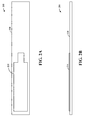
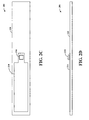
- Figs. 2A-2F show an RFID tag 200 at various stages of manufacture, in accordance with other example embodiments of the present invention.
- the RFID tag 200 may, for example, be implemented using an RFID chip and/or tag as shown in Figure 1 .
- top (2A) and front (2B) views are shown in which a first portion of an antenna circuit 210 is formed on a support structure 220, such as paper or polyethylene.
- Figs. 2C and 2D respectively show top and bottom views, in which an RFID chip 230 has been placed on the antenna circuit 210 as shown. Most or all of a lower surface of the chip 230 is placed in contact with the antenna circuit 210, either directly or via a metallization layer, to facilitate the communication of radio frequency data through the lower surface (e.g., and through a substrate to an RFID circuit such as shown in Fig. 1 and described above).
- Figs. 2E and 2F show an antenna structure after positioning a second portion 212 of an antenna and support structure 222 on top of the lower antenna portion 210 and the RFID chip 230. As indicated by the size of the antenna portion in the area of the RFID chip 230, which is much larger than the actual RFID chip, the positioning of the two antenna portions with respect to each other and to the RFID chip is facilitated, e.g., with low positioning accuracy.
- Fig. 3 shows a cross-section of another RFID tag 300 after lamination, in accordance with another example embodiment of the present invention.
- an integrated circuit 302 is pressed into the upper portion of an antenna.
- An upper antenna 380 on a support structure 382, is laminated to the chip 302 and a lower antenna structure by a laminating material 352.
- a spacer layer (such as in Fig. 1 ) may be implemented to safeguard the distance between active layers of the integrated circuit 302 and the upper portion of the antenna 380, which can minimize parasitic effects.
- the integrated circuit 302 is pressed into the bottom portion of the antenna, and in other implementations, is pressed into both the top and bottom portions of the antenna.
- Fig. 4 shows a cross-section of an RFID tag 400, in accordance with another example embodiment of the present invention.
- the RFID tag 400 includes an RFID chip 402 and an antenna having upper and lower portions 480 and 470 connected thereto, for passing data via transceived radio frequency signals.
- the upper antenna portion 480 is supported by support structure layer 482 (e.g., which may extend around the RFID chip 402, with the structures shown as separate with regard to this cross-section view). Connection between the upper antenna portion 480 and the RFID chip 402 is made via connector 440, with the support structure layer 482 being laminated to the underlying antenna/support structure 470/472 via material 452.
- the support structure layers provide mechanical protection of the RFID chip 402 during assembly (e.g., Cutting or breaking the bottom portion of the antenna, mechanical breaking of the chip), during further processing steps and use in the field.
- FIG. 5 shows a plot of sensitivity versus frequencies of RFID signals passed between an RFID circuit and an antenna portion via a semiconductor substrate, as may be achieved in accordance with this discovery and one or more example embodiments of the present invention.
- Sensitivity (dB) is shown on the vertical axis, and signal frequency is shown on the horizontal axis.
- Plots 510 and 520 represent reference RFID circuits, with plots 530, 540, 550 and 560 representing sample circuits with an antenna portion connection to an RFID circuit in an RFID chip via an underlying substrate of the chip, such as shown herein.
Landscapes
- Engineering & Computer Science (AREA)
- Microelectronics & Electronic Packaging (AREA)
- Computer Hardware Design (AREA)
- Physics & Mathematics (AREA)
- General Physics & Mathematics (AREA)
- Theoretical Computer Science (AREA)
- Semiconductor Integrated Circuits (AREA)
- Variable-Direction Aerials And Aerial Arrays (AREA)
- Support Of Aerials (AREA)
- Details Of Aerials (AREA)
Abstract
Description
- Aspects of various embodiments of the present invention are directed to radio frequency communications, and to apparatuses and methods for radio frequency identification (RFID).
- Radio-frequency communications, such as for radio-frequency identification (RFID), are used in a variety of applications. For example, in RFID applications, communications are effected between a reader and a transponder, with the transponder providing identification (or other) data in response to communications from the reader or in a TTF (tag talks first) mode by powering up. For instance, the transponder can be part of a tag such as an RFID tag (or be the tag), or part of another object affixed to a subject or object to be identified.
- RFID assembly processes require high accuracy during antenna manufacturing (resolution for the contact leads in the die landing area) as well as high placement accuracy during the assembly process as a result of the small IC sizes using standard CMOS processes. In that case, all contact pads for at least one antenna on the IC are placed on an active side of a Silicon (or other base material) wafer in which the RFID circuit is formed. For example, RFID chip sizes can be in the range of 0.2-0.4mm in length/width, with respective contact pads being separated by much smaller distances. Accurately placing such chips can be difficult, resulting in high production costs.
- These and other issues continue to present challenges to the manufacture and implementation of RFID tags and other related circuits.
- Various example embodiments are directed to RFID circuits and their implementation. In accordance with an example embodiment, a radio frequency identification (RFID) tag includes an antenna having first and second antenna portions for transceiving data, and an RFID chip positioned between the first and second antenna portions. The RFID chip includes a semiconductor substrate, an active layer on the semiconductor substrate, and a radio frequency communication circuit (e.g., including doped regions of the active layer). The semiconductor substrate has a lower surface area that faces the first antenna portion and communicates data, carried by radio frequency signals, between the first antenna portion and the radio frequency communication circuit. A conductor connects the radio frequency communication circuit to the second antenna portion, to facilitate communication of the data carried by radio frequency signals between the second antenna portion and the radio frequency communication circuit.
- Another example embodiment is directed to a radio frequency communication circuit having an antenna with a planar conductor, and a semiconductor chip having an active semiconductor layer on a bulk semiconductor substrate. The active semiconductor region includes a radio frequency communication circuit, and the semiconductor substrate has a planar lower surface area that is parallel to the planar conductor, with most or all of the lower surface area being in direct contact with the planar conductor. The radio frequency communication circuit, planar conductor and semiconductor substrate are configured and arranged together to pass data, carried by radio frequency signals, between the antenna and the radio frequency communication circuit via the semiconductor substrate.
- Another example embodiment is directed to a method of manufacturing an apparatus. About all of a lower surface of an RFID chip is connected to a first antenna portion, and the RFID chip is electrically connected to the first antenna portion. The RFID chip has a radio frequency circuit in an active layer at an upper surface of the RFID chip that is on an underlying substrate, and opposite the lower surface of the RFID chip. The lower surface and the first antenna connection are connected for communicating data carried by radio frequency signals between the first antenna connection and the radio frequency circuit through the substrate. A second antenna portion is laminated to the first antenna portion and electrically connected to an upper surface of the RFID chip, using a laminating material to secure the second antenna portion to the upper surface and extending a conductive contact through the laminating material to connect the second antenna portion to a radio frequency circuit at the upper surface.
- The above discussion/summary is not intended to describe each embodiment or every implementation of the present disclosure. The figures and detailed description that follow also exemplify various embodiments.
- Various example embodiments may be more completely understood in consideration of the following detailed description in connection with the accompanying drawings, in which:
-
Fig. 1 shows an RFID tag having a radio frequency circuit coupled to an antenna portion via a semiconductor substrate, in accordance with an example embodiment of the present invention; -
Figs. 2A-2F show an RFID tag at various stages of manufacture, in accordance with other example embodiments of the present invention; -
Fig. 3 shows an RFID tag, in accordance with another example embodiment of the present invention; -
Fig. 4 shows an RFID tag, in accordance with another example embodiment of the present invention; and -
Fig. 5 shows a plot of sensitivity versus frequencies of RFID signals passed between an RFID circuit and an antenna portion via a semiconductor substrate, in accordance with another example embodiment of the present invention. - While the invention is amenable to various modifications and alternative forms, specifics thereof have been shown by way of example in the drawings and will be described in detail. It should be understood, however, that the intention is not to limit the invention to the particular embodiments described. On the contrary, the intention is to cover all modifications, equivalents, and alternatives falling within the scope of the invention including aspects defined in the claims. In addition, the term "example" as used throughout this application is only by way of illustration, and not limitation.
- Aspects of the present invention are believed to be applicable to a variety of different types of devices, systems and arrangements involving radio frequency communications, and to such devices employing radio frequency identification (RFID). While the present invention is not necessarily so limited, various aspects of the invention may be appreciated through a discussion of examples using this context.
- Various example embodiments are directed to an RFID device having a circuit-to-antenna connection that is through a substrate upon which circuit components of the RFID device are formed. In some implementations, the RFID device is an RFID tag in which an RFID chip is laminated between respective antenna portions on opposing surfaces of the chip, and with at least one of the antenna portions connected to circuit components of the RFID device via an underlying substrate in the chip and upon which the circuit is formed.
- Accordingly, the substrate passes radio frequency signals that are received at the antenna, through the substrate to the circuit components (e.g., corresponding to a voltage induced at the antenna). This can be accomplished without necessarily employing a conductor extending through the underlying substrate for contacting the antenna portion. In addition, contact between the RFID chip and the antenna can be made through a surface of such an underlying substrate, which mitigates alignment issues with conductors/vias extending through the substrate, and which can be useful for addressing challenges including those discussed above. In addition, such an RFID chip can be manufactured using CMOS type device processing, which may employ connector/bump type structures (e.g., stitch bump, Aubump, or Cu-pillar, Solderballs) for front-side connection to an antenna with through-substrate connection to a back-side antenna.
- In connection with one or more embodiments, it has been discovered that connection between an antenna and active regions of an integrated circuit chip can be made through a substrate upon which the active regions are formed. In this context, various embodiments are directed to apparatuses including antennas respectively coupled to communicate radio frequency data to active regions of an integrated circuit chip, by way of an underlying substrate.
- A more particular example embodiment is directed to a radio frequency circuit, as may involve RFID communications, having an antenna with a planar conductor connected to a lower surface of a semiconductor chip for communicating data carried by radio frequency signals, via a backside substrate of the chip, to a front-side active layer in which radio frequency circuitry lies. Most or all of the lower surface area is in direct contact with the planar conductor, in contact via a metallization layer or capacitively coupled with the planar conductor. Another conductor can be connected with the front-side active layer (e.g., via a direct conductor, such as a conductive bump or other circuit), and act with the planar conductor to communicate radio frequency signals. The respective antenna portions are laminated to the chip. Further, data communications between the planar conductor on the backside and the active layer (and forming an antenna loop with the other conductor) can be limited to the backside substrate. In addition, such communications can be effected for powering the radio frequency circuit via wireless RF signals received at the antenna, for transceiving radio frequency signals.
- A more particular example embodiment is directed to a radio frequency identification (RFID) tag having an antenna with first and second antenna portions for transceiving data, and a RFID chip positioned between the antenna portions. The chip includes an active layer on a semiconductor substrate, with a radio frequency communication circuit including doped regions of the active layer. A lower surface area of the chip (or a conductive layer thereupon) is in contact with the first antenna portion and communicates data, carried by radio frequency signals, between the first antenna portion and the radio frequency communication circuit (e.g., all or almost all of the data is communicated via the substrate and closed-loop connection with the second antenna portion). The second antenna portion is connected to the radio frequency communication circuit via a conductor at an upper surface of the chip. In some implementations, radio frequency signals communicated via the antenna portions are also used to power the chip. As applicable here and to other example embodiments, reference to lower and upper components is by way of example, and the respective components being in alternate orientations (e.g., with lower and upper being left and right, or swapping lower and upper by flipping a device upside down).
- The antenna portions are coupled to the chip and to one another, with different arrangements, in accordance with various example embodiments. In some implementations, the antenna portions are connected to a support structure such as paper or plastic, and laminated to the chip and to each other, and can be wrapped around sidewalls of the chip. In various embodiments, the respective antenna portions are formed with geometric shapes that facilitate coupling (and laminating) of the chip in a very thin package.
- Other embodiments are directed to manufacturing an apparatus having radio frequency communication circuits. About all of a lower surface of an RFID chip as discussed herein (e.g., with or without a conductive layer thereupon) is laminated to a first antenna portion, and a second antenna portion is laminated to an upper surface of the RFID chip. The lamination is carried out such that the lower surface and the first antenna communicate data carried by radio frequency signals between the first antenna and a radio frequency circuit in the chip, through a backside substrate.
- Turning now to the figures,
Fig. 1 shows a cross-sectional view of anRFID tag 100 having a radio frequency circuit coupled to an antenna via a substrate, in accordance with another example embodiment of the present invention. Thetag 100 includes anRFID chip 102 having RFID circuitry inactive layer 110 that is formed on anunderlying substrate 120. A passivation layer 130 (e.g., with silicon oxide and/or silicon nitride) is on theactive layer 110, and acontact 140 that extends above the passivation layer provides an electrical connection to theactive layer 110 via acontact pad 142. - The
chip 102 is positioned between lower andupper antenna portions structures lamination material 150, such as an insulating glue, secures theupper antenna portion 180 to thechip 102 and to contact 140, making an electrical connection between the upper antenna portion and theactive layer 110. Thecontact 140 thus extends through thelamination material 150, which can be effected by pressing the upper antenna portion (and supporting structure 182) firmly against thechip 102. The connection between thecontact 140 andupper antenna portion 180 is made in one or more of a variety of manners, such as by conductive gluing, anisotropic conduction gluing, a pure metallic interconnection, soldering or capacitive coupling. In some instances, thelamination material 150 acts as a spacer layer and is penetrated by thecontact 140. In this case the spacer layer reduces parasitic coupling between dedicated circuitry blocks in theactive layers 110 and theupper antenna portion 180. Anoptional spacer layer 152 is shown formed at an upper portion of thechip 102, and can be implemented to electrically insulate components thereupon (e.g., unused contact pads). Thechip 102 is electrically connected to the lower antenna portion 170 (and may be at least temporarily coupled via an adhesive type material 174). - The lower surface 121 of the
substrate 120 passes data carried by radio frequency signals from thelower antenna portion 170, to theactive layers 110. With this approach, thesubstrate 120 acts as a conduit for coupling data received via the antenna portion 170 (and, as relevant toantenna portion 180 acting therewith), to theactive layers 110. In addition, while thechip 102 is shown with anoptional metallization layer 160 in contact with thelower antenna portion 170 and a lower surface of thesubstrate 120, the metallization layer is omitted in various implementations in which the lower surface of the substrate is in direct contact with the lower antenna portion. In still other implementations, the lower surface 121 is fitted with a bump structure, which may include a plurality of conductors similar to thecontact 140, for facilitating contact. - The
antenna portions structures - The thickness of the
substrate 120 is set to facilitate communication of the data, via radio frequency signals, from thelower antenna portion 170 and the active region (layers) 110. In some implementations, thesubstrate 120 is thinned to a set thickness, such as 150 micrometers, or less. -
Figs. 2A-2F show anRFID tag 200 at various stages of manufacture, in accordance with other example embodiments of the present invention. TheRFID tag 200 may, for example, be implemented using an RFID chip and/or tag as shown inFigure 1 . Beginning withFigs. 2A and 2B , top (2A) and front (2B) views are shown in which a first portion of anantenna circuit 210 is formed on asupport structure 220, such as paper or polyethylene. -
Figs. 2C and 2D respectively show top and bottom views, in which anRFID chip 230 has been placed on theantenna circuit 210 as shown. Most or all of a lower surface of thechip 230 is placed in contact with theantenna circuit 210, either directly or via a metallization layer, to facilitate the communication of radio frequency data through the lower surface (e.g., and through a substrate to an RFID circuit such as shown inFig. 1 and described above). -
Figs. 2E and 2F show an antenna structure after positioning asecond portion 212 of an antenna andsupport structure 222 on top of thelower antenna portion 210 and theRFID chip 230. As indicated by the size of the antenna portion in the area of theRFID chip 230, which is much larger than the actual RFID chip, the positioning of the two antenna portions with respect to each other and to the RFID chip is facilitated, e.g., with low positioning accuracy. -
Fig. 3 shows a cross-section of anotherRFID tag 300 after lamination, in accordance with another example embodiment of the present invention. In this figure anintegrated circuit 302 is pressed into the upper portion of an antenna. Anupper antenna 380, on asupport structure 382, is laminated to thechip 302 and a lower antenna structure by alaminating material 352. A spacer layer (such as inFig. 1 ) may be implemented to safeguard the distance between active layers of theintegrated circuit 302 and the upper portion of theantenna 380, which can minimize parasitic effects. In some implementations, theintegrated circuit 302 is pressed into the bottom portion of the antenna, and in other implementations, is pressed into both the top and bottom portions of the antenna. These implementations can be facilitated by using substrate materials with different hardness and/or different temperatures during lamination for heating the upper and the lower substrate, which is also used in various embodiments to control the imprint of the integrated circuit 302 (e.g., such that thebump 140 inFig. 1 is pressed into theupper antenna portion 180, whereas no or only little imprint of theintegrated circuit 302 into the lower antenna portion is allowed to mitigate/prevent the lower antenna portion from being cut/broken around the integrated circuit, which can result in malfunction).Fig. 4 shows a cross-section of anRFID tag 400, in accordance with another example embodiment of the present invention. TheRFID tag 400 includes anRFID chip 402 and an antenna having upper andlower portions upper antenna portion 480 is supported by support structure layer 482 (e.g., which may extend around theRFID chip 402, with the structures shown as separate with regard to this cross-section view). Connection between theupper antenna portion 480 and theRFID chip 402 is made viaconnector 440, with thesupport structure layer 482 being laminated to the underlying antenna/support structure 470/472 viamaterial 452. In this case, the support structure layers provide mechanical protection of theRFID chip 402 during assembly (e.g., Cutting or breaking the bottom portion of the antenna, mechanical breaking of the chip), during further processing steps and use in the field. - As discussed above, in connection with various embodiments it has been discovered that sufficient radio frequency signal coupling can be effected via an underlying substrate, to facilitate data communications via the radio frequency signal coupling.
Figure 5 shows a plot of sensitivity versus frequencies of RFID signals passed between an RFID circuit and an antenna portion via a semiconductor substrate, as may be achieved in accordance with this discovery and one or more example embodiments of the present invention. Sensitivity (dB) is shown on the vertical axis, and signal frequency is shown on the horizontal axis.Plots plots - Based upon the above discussion and illustrations, those skilled in the art will readily recognize that various modifications and changes may be made to the present invention without strictly following the exemplary embodiments and applications illustrated and described herein. For example, other types of communication can be effected via a substrate, for devices and applications that may not necessarily involve radio frequency and RFID. In addition, a variety of different types of RFID circuits can be used in connection with the structures shown herein (e.g., with the RFID circuits shown in the active layers of the respective RFID chips shown in the figures). For general information regarding radio frequency communications, and for specific information regarding RFID circuits (or functionality thereof) that may be implemented in accordance with one or more example embodiments, reference maybe made to
U.S. Patent Application Serial No. 6,815,809 , which is fully incorporated herein by reference. Such modifications do not depart from the true spirit and scope of the present invention, including that set forth in the following claims.
Claims (15)
- A radio frequency identification (RFID) tag comprising
an antenna having first and second antenna portions and configured and arranged for transceiving data;
an RFID chip laminated between the first and second antenna portions, the RFID chip including a semiconductor substrate, an active layer on the semiconductor substrate, and a radio frequency communication circuit, the semiconductor substrate being configured and arranged with a lower surface area that faces the first antenna portion and communicates data, carried by radio frequency signals, between the first antenna portion and the radio frequency communication circuit; and
a conductor that connects the radio frequency communication circuit to the second antenna portion, the conductor being configured and arranged with the semiconductor substrate to communicate the data carried by radio frequency signals between the second antenna portion and the radio frequency communication circuit. - The RFID tag of claim 1, wherein, the radio frequency communications circuit includes doped regions of the active layer, and substantially all radio frequency signals communicated via the first antenna portion are passed from the lower surface area to the doped regions via the semiconductor substrate.
- The RFID tag of claim 1, wherein the radio frequency communication circuit is configured and arranged to use the radio frequency signals to generate power for operating the radio frequency communication circuit.
- The RFID tag of claim 1, wherein the entire lower surface is in direct contact with a surface of the first antenna portion.
- The RFID tag of claim 1, further including a conductive layer on the lower surface, in direct contact with the first antenna portion, and configured and arranged to conduct the radio frequency signals between the first antenna portion and the lower surface.
- The RFID tag of claim 1, wherein the first antenna portion is connected to a surface of a first material and the second antenna portion is connected to a surface of a second material that faces the surface of the first material, the second material being laminated to the RFID chip and to the surface of the first material.
- The RFID tag of claim 1, further including a passivation layer between the RFID chip and the second antenna portion.
- The RFID tag of claim 1, further including a laminating material configured and arranged to connect the second antenna portion to the RFID chip and to electrically insulate the second antenna portion from portions of the RFID chip.
- The RFID tag of claim 8, wherein the second antenna portion is on a material that is in contact with the laminating material and wraps around sidewalls of the RFID chip that extend between the lower surface and an upper surface at which the radio frequency circuit is located.
- The RFID tag of claim 1, wherein the semiconductor substrate between the radio frequency communication circuit and the lower surface area has a thickness of less than about 150 micrometers.
- The RFID tag of claim 1, wherein the radio frequency circuit is configured and arranged to, in response to data received via the antenna, generate and transmit data in the form of radio frequency signals via the substrate and the antenna.
- A radio frequency communication circuit comprising
a semiconductor chip having an active semiconductor layer on a bulk semiconductor substrate, the active semiconductor region including radio frequency circuit components, the semiconductor substrate having a lower surface area, about all of the lower surface area being in electrical contact with an antenna conductor, and the radio frequency communication circuit and semiconductor substrate being configured and arranged together to pass data, carried by radio frequency signals, between the antenna conductor and the radio frequency circuit components via the semiconductor substrate. - The circuit of claim 12, further including an antenna including the antenna conductor and another conductor in contact with the radio frequency circuit components via an upper surface of the semiconductor chip, the respective conductors being laminated to one another and to the semiconductor ship to form a laminated radio frequency circuit.
- The circuit of claim 12, wherein the semiconductor chip is configured and arranged to pass all data communications between the antenna conductor and the radio frequency circuit components via semiconductor material in the semiconductor substrate to well regions in the active semiconductor region, the well regions being part of the radio frequency circuit components.
- The circuit of claim 12, wherein the radio frequency communication circuit is configured and arranged to
use radio frequency signals received via the substrate to generate power for operating the radio frequency circuit components, and
in response to data received via the antenna conductor, generate and transmit data in the form of radio frequency signals via the substrate and the antenna conductor.
Applications Claiming Priority (1)
| Application Number | Priority Date | Filing Date | Title |
|---|---|---|---|
| US13/449,069 US8628018B2 (en) | 2012-04-17 | 2012-04-17 | RFID circuit and method |
Publications (3)
| Publication Number | Publication Date |
|---|---|
| EP2654001A2 true EP2654001A2 (en) | 2013-10-23 |
| EP2654001A3 EP2654001A3 (en) | 2015-09-30 |
| EP2654001B1 EP2654001B1 (en) | 2017-09-27 |
Family
ID=48087438
Family Applications (1)
| Application Number | Title | Priority Date | Filing Date |
|---|---|---|---|
| EP13163143.4A Active EP2654001B1 (en) | 2012-04-17 | 2013-04-10 | RFID circuit and method |
Country Status (3)
| Country | Link |
|---|---|
| US (1) | US8628018B2 (en) |
| EP (1) | EP2654001B1 (en) |
| CN (1) | CN103377395B (en) |
Families Citing this family (22)
| Publication number | Priority date | Publication date | Assignee | Title |
|---|---|---|---|---|
| EP2836878B1 (en) * | 2012-04-11 | 2019-02-27 | IMPINJ, Inc. | Rfid integrated circuits and tags with antenna contacts on multiple surfaces |
| US10311351B1 (en) | 2012-04-11 | 2019-06-04 | Impinj, Inc. | RFID integrated circuits with antenna contacts on multiple surfaces |
| US9053400B2 (en) | 2012-04-11 | 2015-06-09 | Impinj, Inc. | RFID integrated circuits with antenna contacts on multiple surfaces |
| US20140144992A1 (en) * | 2012-09-10 | 2014-05-29 | Impinj, Inc. | Rfid integrated circuits and tags with antenna contacts on multiple surfaces |
| US20140070010A1 (en) * | 2012-09-10 | 2014-03-13 | Impinj, Inc. | Rfid integrated circuits with antenna contacts on multiple surfaces |
| FR3021145B1 (en) * | 2014-05-14 | 2018-08-31 | Linxens Holding | METHOD FOR MANUFACTURING A CIRCUIT FOR A CHIP CARD MODULE AND CIRCUIT FOR A CHIP CARD MODULE |
| US20160004952A1 (en) * | 2014-07-02 | 2016-01-07 | VivaLnk, Inc. | Wearable tag capable of wireless communications |
| US10860909B2 (en) | 2016-04-05 | 2020-12-08 | Hewlett-Packard Development Company, L.P. | Modular radio frequency identification (RFID) devices |
| CN110622628B (en) * | 2017-03-15 | 2021-10-26 | 香港物流及供应链管理应用技术研发中心 | Radio frequency communication guiding device |
| US10671969B2 (en) | 2017-05-03 | 2020-06-02 | Summate Technologies, Inc. | Operating room situated, parts-inventory control system and supervisory arrangement for accurately tracking the use of and accounting for the ultimate disposition of an individual component part of a complete implant which is then being surgically engrafted in-vivo upon or into the body of a living subject |
| CN209963236U (en) * | 2017-09-29 | 2020-01-17 | 株式会社村田制作所 | Wireless communication device |
| CN108009619A (en) * | 2017-12-27 | 2018-05-08 | 上海数斐信息科技有限公司 | A kind of RF tag |
| BR112020021426A2 (en) * | 2018-04-20 | 2021-01-19 | Avery Dennison Retail Information Services, Llc | RFID BELTS WITH A TOP AND BOTTOM CONDUCTOR |
| US10470809B1 (en) | 2018-06-19 | 2019-11-12 | Summate Technologies, Inc. | Automated screw identification system and method |
| CN110931938B (en) * | 2018-09-20 | 2021-04-16 | 宏碁股份有限公司 | Electronic device |
| US10664734B2 (en) * | 2018-10-22 | 2020-05-26 | Graphene Security Limited | High-frequency-NFC-based product traceability and anti-counterfeiting tag |
| US10909343B1 (en) | 2019-07-12 | 2021-02-02 | Summate Technologies, Inc. | Automated screw identification system and method with labeled pegs |
| JP7377490B2 (en) * | 2019-11-19 | 2023-11-10 | 大王製紙株式会社 | RFID tag |
| JP7624005B2 (en) | 2019-12-30 | 2025-01-29 | エイヴェリー デニソン リテール インフォメーション サービシズ リミテッド ライアビリティ カンパニー | Metal Detector Resistant RFID Tags |
| US12585909B2 (en) * | 2021-08-12 | 2026-03-24 | Puneet KAPOOR | Wire embedded label on special substrate with or without inductive coupling |
| CN113808957B (en) * | 2021-09-17 | 2024-05-03 | 成都奕成集成电路有限公司 | Chip packaging method, chip packaging structure and electronic equipment |
| CN113808956B (en) * | 2021-09-17 | 2024-05-03 | 成都奕成集成电路有限公司 | Chip packaging method, chip packaging structure and electronic equipment |
Citations (1)
| Publication number | Priority date | Publication date | Assignee | Title |
|---|---|---|---|---|
| US6815809B2 (en) | 2001-03-16 | 2004-11-09 | Koninklijke Philips Electronics N.V. | Portable electronic device |
Family Cites Families (14)
| Publication number | Priority date | Publication date | Assignee | Title |
|---|---|---|---|---|
| JP3150575B2 (en) | 1995-07-18 | 2001-03-26 | 沖電気工業株式会社 | Tag device and manufacturing method thereof |
| AU5809099A (en) * | 1998-09-11 | 2000-04-03 | Motorola, Inc. | Radio frequency identification tag apparatus and related method |
| US6407669B1 (en) | 2001-02-02 | 2002-06-18 | 3M Innovative Properties Company | RFID tag device and method of manufacturing |
| US6900536B1 (en) | 2002-04-26 | 2005-05-31 | Celis Semiconductor Corporation | Method for producing an electrical circuit |
| JP2004362190A (en) * | 2003-06-04 | 2004-12-24 | Hitachi Ltd | Semiconductor device |
| KR20070046191A (en) * | 2004-08-26 | 2007-05-02 | 코닌클리즈케 필립스 일렉트로닉스 엔.브이. | Circuit arrays and manufacturing method thereof |
| CA2600458A1 (en) * | 2005-03-07 | 2006-09-14 | Sensormatic Electronics Corporation | Automated tuning method for rfid labels |
| ATE481690T1 (en) * | 2005-03-21 | 2010-10-15 | Nxp Bv | RFID LABELING AND METHOD FOR PRODUCING AN RFID LABEL |
| EP1913530B1 (en) * | 2005-08-02 | 2014-10-08 | Nxp B.V. | Antenna structure, transponder and method of manufacturing an antenna structure |
| US8067253B2 (en) * | 2005-12-21 | 2011-11-29 | Avery Dennison Corporation | Electrical device and method of manufacturing electrical devices using film embossing techniques to embed integrated circuits into film |
| CN101460962B (en) * | 2006-06-02 | 2011-01-12 | 株式会社日立制作所 | Method for manufacturing inlet for IC tag |
| US8866616B2 (en) * | 2007-08-22 | 2014-10-21 | Tyco Fire & Security Gmbh | RFID tag having antenna with co-planar radiation pattern |
| KR101102682B1 (en) * | 2009-12-23 | 2012-01-05 | 주식회사 하이닉스반도체 | Antenna of the RFID device |
| EP2410565A1 (en) | 2010-07-21 | 2012-01-25 | Nxp B.V. | Component to connection to an antenna |
-
2012
- 2012-04-17 US US13/449,069 patent/US8628018B2/en active Active
-
2013
- 2013-04-10 EP EP13163143.4A patent/EP2654001B1/en active Active
- 2013-04-11 CN CN201310125113.XA patent/CN103377395B/en active Active
Patent Citations (1)
| Publication number | Priority date | Publication date | Assignee | Title |
|---|---|---|---|---|
| US6815809B2 (en) | 2001-03-16 | 2004-11-09 | Koninklijke Philips Electronics N.V. | Portable electronic device |
Also Published As
| Publication number | Publication date |
|---|---|
| US8628018B2 (en) | 2014-01-14 |
| US20130270348A1 (en) | 2013-10-17 |
| EP2654001A3 (en) | 2015-09-30 |
| EP2654001B1 (en) | 2017-09-27 |
| CN103377395B (en) | 2016-08-24 |
| CN103377395A (en) | 2013-10-30 |
Similar Documents
| Publication | Publication Date | Title |
|---|---|---|
| EP2654001B1 (en) | RFID circuit and method | |
| US20220148951A1 (en) | Semiconductor device including an antenna | |
| US10885421B1 (en) | RFID integrated circuits with antenna contacts on multiple surfaces | |
| US7823322B2 (en) | Silicon chip having inclined contact pads and electronic module comprising such a chip | |
| US9984985B1 (en) | Semiconductor package device with antenna array | |
| US11875210B2 (en) | Wireless communication device and method of manufacturing same | |
| EP2458530B1 (en) | Transponder tagged object and method for its manufacturing | |
| US8959759B2 (en) | Method for assembling computer modules small in thickness | |
| EP1930844B1 (en) | Noncontact information storage medium and method for manufacturing same | |
| US8278154B2 (en) | Method of fabricating a semiconductor device package including a heat radiation plate | |
| TW200910556A (en) | Method for connecting an electronic chip to a radiofrequency identification device | |
| JP5103127B2 (en) | RFID tag | |
| EP3836207B1 (en) | Semiconductor structure and method for manufacturing a semiconductor structure | |
| US8723744B2 (en) | Method for making contactless portable devices with dielectric bridge and portable devices | |
| US20250087606A1 (en) | Semiconductor device package comprising antenna and communication module | |
| US8169285B2 (en) | Semiconductor device with integrated coils | |
| US12499343B2 (en) | Wafer-level package sensor device | |
| US11811131B2 (en) | Antenna module | |
| US20080296745A1 (en) | Semiconductor device having semiconductor chip and antenna | |
| JP7447662B2 (en) | IC card | |
| US11581273B2 (en) | Semiconductor device package and method of manufacturing the same | |
| US11329016B2 (en) | Semiconductor device package and method of manufacturing the same | |
| JP2005348197A (en) | Radio electronic device | |
| US8778776B2 (en) | Methods of forming a semiconductor package using a seed layer and semiconductor packages formed using the same | |
| EP3079105B1 (en) | Dual-interface ic card components and method for manufacturing the dual-interface ic card components |
Legal Events
| Date | Code | Title | Description |
|---|---|---|---|
| PUAI | Public reference made under article 153(3) epc to a published international application that has entered the european phase |
Free format text: ORIGINAL CODE: 0009012 |
|
| AK | Designated contracting states |
Kind code of ref document: A2 Designated state(s): AL AT BE BG CH CY CZ DE DK EE ES FI FR GB GR HR HU IE IS IT LI LT LU LV MC MK MT NL NO PL PT RO RS SE SI SK SM TR |
|
| AX | Request for extension of the european patent |
Extension state: BA ME |
|
| 17P | Request for examination filed |
Effective date: 20140326 |
|
| PUAL | Search report despatched |
Free format text: ORIGINAL CODE: 0009013 |
|
| AK | Designated contracting states |
Kind code of ref document: A3 Designated state(s): AL AT BE BG CH CY CZ DE DK EE ES FI FR GB GR HR HU IE IS IT LI LT LU LV MC MK MT NL NO PL PT RO RS SE SI SK SM TR |
|
| AX | Request for extension of the european patent |
Extension state: BA ME |
|
| RIC1 | Information provided on ipc code assigned before grant |
Ipc: H01L 21/56 20060101ALI20150824BHEP Ipc: G06K 19/077 20060101AFI20150824BHEP Ipc: H01Q 1/22 20060101ALI20150824BHEP |
|
| RBV | Designated contracting states (corrected) |
Designated state(s): AL AT BE BG CH CY CZ DE DK EE ES FI FR GB GR HR HU IE IS IT LI LT LU LV MC MK MT NL NO PL PT RO RS SE SI SK SM TR |
|
| 17Q | First examination report despatched |
Effective date: 20170404 |
|
| GRAP | Despatch of communication of intention to grant a patent |
Free format text: ORIGINAL CODE: EPIDOSNIGR1 |
|
| INTG | Intention to grant announced |
Effective date: 20170622 |
|
| GRAS | Grant fee paid |
Free format text: ORIGINAL CODE: EPIDOSNIGR3 |
|
| GRAA | (expected) grant |
Free format text: ORIGINAL CODE: 0009210 |
|
| AK | Designated contracting states |
Kind code of ref document: B1 Designated state(s): AL AT BE BG CH CY CZ DE DK EE ES FI FR GB GR HR HU IE IS IT LI LT LU LV MC MK MT NL NO PL PT RO RS SE SI SK SM TR |
|
| REG | Reference to a national code |
Ref country code: GB Ref legal event code: FG4D |
|
| REG | Reference to a national code |
Ref country code: CH Ref legal event code: EP |
|
| REG | Reference to a national code |
Ref country code: AT Ref legal event code: REF Ref document number: 932628 Country of ref document: AT Kind code of ref document: T Effective date: 20171015 |
|
| REG | Reference to a national code |
Ref country code: IE Ref legal event code: FG4D |
|
| REG | Reference to a national code |
Ref country code: DE Ref legal event code: R096 Ref document number: 602013027045 Country of ref document: DE |
|
| PG25 | Lapsed in a contracting state [announced via postgrant information from national office to epo] |
Ref country code: FI Free format text: LAPSE BECAUSE OF FAILURE TO SUBMIT A TRANSLATION OF THE DESCRIPTION OR TO PAY THE FEE WITHIN THE PRESCRIBED TIME-LIMIT Effective date: 20170927 Ref country code: SE Free format text: LAPSE BECAUSE OF FAILURE TO SUBMIT A TRANSLATION OF THE DESCRIPTION OR TO PAY THE FEE WITHIN THE PRESCRIBED TIME-LIMIT Effective date: 20170927 Ref country code: NO Free format text: LAPSE BECAUSE OF FAILURE TO SUBMIT A TRANSLATION OF THE DESCRIPTION OR TO PAY THE FEE WITHIN THE PRESCRIBED TIME-LIMIT Effective date: 20171227 Ref country code: LT Free format text: LAPSE BECAUSE OF FAILURE TO SUBMIT A TRANSLATION OF THE DESCRIPTION OR TO PAY THE FEE WITHIN THE PRESCRIBED TIME-LIMIT Effective date: 20170927 Ref country code: HR Free format text: LAPSE BECAUSE OF FAILURE TO SUBMIT A TRANSLATION OF THE DESCRIPTION OR TO PAY THE FEE WITHIN THE PRESCRIBED TIME-LIMIT Effective date: 20170927 |
|
| REG | Reference to a national code |
Ref country code: NL Ref legal event code: MP Effective date: 20170927 |
|
| REG | Reference to a national code |
Ref country code: LT Ref legal event code: MG4D |
|
| REG | Reference to a national code |
Ref country code: AT Ref legal event code: MK05 Ref document number: 932628 Country of ref document: AT Kind code of ref document: T Effective date: 20170927 |
|
| PG25 | Lapsed in a contracting state [announced via postgrant information from national office to epo] |
Ref country code: BG Free format text: LAPSE BECAUSE OF FAILURE TO SUBMIT A TRANSLATION OF THE DESCRIPTION OR TO PAY THE FEE WITHIN THE PRESCRIBED TIME-LIMIT Effective date: 20171227 Ref country code: GR Free format text: LAPSE BECAUSE OF FAILURE TO SUBMIT A TRANSLATION OF THE DESCRIPTION OR TO PAY THE FEE WITHIN THE PRESCRIBED TIME-LIMIT Effective date: 20171228 Ref country code: LV Free format text: LAPSE BECAUSE OF FAILURE TO SUBMIT A TRANSLATION OF THE DESCRIPTION OR TO PAY THE FEE WITHIN THE PRESCRIBED TIME-LIMIT Effective date: 20170927 Ref country code: RS Free format text: LAPSE BECAUSE OF FAILURE TO SUBMIT A TRANSLATION OF THE DESCRIPTION OR TO PAY THE FEE WITHIN THE PRESCRIBED TIME-LIMIT Effective date: 20170927 |
|
| REG | Reference to a national code |
Ref country code: FR Ref legal event code: PLFP Year of fee payment: 6 |
|
| PG25 | Lapsed in a contracting state [announced via postgrant information from national office to epo] |
Ref country code: NL Free format text: LAPSE BECAUSE OF FAILURE TO SUBMIT A TRANSLATION OF THE DESCRIPTION OR TO PAY THE FEE WITHIN THE PRESCRIBED TIME-LIMIT Effective date: 20170927 |
|
| PG25 | Lapsed in a contracting state [announced via postgrant information from national office to epo] |
Ref country code: RO Free format text: LAPSE BECAUSE OF FAILURE TO SUBMIT A TRANSLATION OF THE DESCRIPTION OR TO PAY THE FEE WITHIN THE PRESCRIBED TIME-LIMIT Effective date: 20170927 Ref country code: CZ Free format text: LAPSE BECAUSE OF FAILURE TO SUBMIT A TRANSLATION OF THE DESCRIPTION OR TO PAY THE FEE WITHIN THE PRESCRIBED TIME-LIMIT Effective date: 20170927 Ref country code: ES Free format text: LAPSE BECAUSE OF FAILURE TO SUBMIT A TRANSLATION OF THE DESCRIPTION OR TO PAY THE FEE WITHIN THE PRESCRIBED TIME-LIMIT Effective date: 20170927 |
|
| PG25 | Lapsed in a contracting state [announced via postgrant information from national office to epo] |
Ref country code: AT Free format text: LAPSE BECAUSE OF FAILURE TO SUBMIT A TRANSLATION OF THE DESCRIPTION OR TO PAY THE FEE WITHIN THE PRESCRIBED TIME-LIMIT Effective date: 20170927 Ref country code: IT Free format text: LAPSE BECAUSE OF FAILURE TO SUBMIT A TRANSLATION OF THE DESCRIPTION OR TO PAY THE FEE WITHIN THE PRESCRIBED TIME-LIMIT Effective date: 20170927 Ref country code: EE Free format text: LAPSE BECAUSE OF FAILURE TO SUBMIT A TRANSLATION OF THE DESCRIPTION OR TO PAY THE FEE WITHIN THE PRESCRIBED TIME-LIMIT Effective date: 20170927 Ref country code: IS Free format text: LAPSE BECAUSE OF FAILURE TO SUBMIT A TRANSLATION OF THE DESCRIPTION OR TO PAY THE FEE WITHIN THE PRESCRIBED TIME-LIMIT Effective date: 20180127 Ref country code: SK Free format text: LAPSE BECAUSE OF FAILURE TO SUBMIT A TRANSLATION OF THE DESCRIPTION OR TO PAY THE FEE WITHIN THE PRESCRIBED TIME-LIMIT Effective date: 20170927 Ref country code: SM Free format text: LAPSE BECAUSE OF FAILURE TO SUBMIT A TRANSLATION OF THE DESCRIPTION OR TO PAY THE FEE WITHIN THE PRESCRIBED TIME-LIMIT Effective date: 20170927 |
|
| REG | Reference to a national code |
Ref country code: DE Ref legal event code: R097 Ref document number: 602013027045 Country of ref document: DE |
|
| PG25 | Lapsed in a contracting state [announced via postgrant information from national office to epo] |
Ref country code: DK Free format text: LAPSE BECAUSE OF FAILURE TO SUBMIT A TRANSLATION OF THE DESCRIPTION OR TO PAY THE FEE WITHIN THE PRESCRIBED TIME-LIMIT Effective date: 20170927 |
|
| PLBE | No opposition filed within time limit |
Free format text: ORIGINAL CODE: 0009261 |
|
| STAA | Information on the status of an ep patent application or granted ep patent |
Free format text: STATUS: NO OPPOSITION FILED WITHIN TIME LIMIT |
|
| PG25 | Lapsed in a contracting state [announced via postgrant information from national office to epo] |
Ref country code: PL Free format text: LAPSE BECAUSE OF FAILURE TO SUBMIT A TRANSLATION OF THE DESCRIPTION OR TO PAY THE FEE WITHIN THE PRESCRIBED TIME-LIMIT Effective date: 20170927 |
|
| 26N | No opposition filed |
Effective date: 20180628 |
|
| PG25 | Lapsed in a contracting state [announced via postgrant information from national office to epo] |
Ref country code: SI Free format text: LAPSE BECAUSE OF FAILURE TO SUBMIT A TRANSLATION OF THE DESCRIPTION OR TO PAY THE FEE WITHIN THE PRESCRIBED TIME-LIMIT Effective date: 20170927 Ref country code: MC Free format text: LAPSE BECAUSE OF FAILURE TO SUBMIT A TRANSLATION OF THE DESCRIPTION OR TO PAY THE FEE WITHIN THE PRESCRIBED TIME-LIMIT Effective date: 20170927 |
|
| REG | Reference to a national code |
Ref country code: CH Ref legal event code: PL |
|
| REG | Reference to a national code |
Ref country code: BE Ref legal event code: MM Effective date: 20180430 |
|
| GBPC | Gb: european patent ceased through non-payment of renewal fee |
Effective date: 20180410 |
|
| REG | Reference to a national code |
Ref country code: IE Ref legal event code: MM4A |
|
| PG25 | Lapsed in a contracting state [announced via postgrant information from national office to epo] |
Ref country code: LU Free format text: LAPSE BECAUSE OF NON-PAYMENT OF DUE FEES Effective date: 20180410 |
|
| PG25 | Lapsed in a contracting state [announced via postgrant information from national office to epo] |
Ref country code: CH Free format text: LAPSE BECAUSE OF NON-PAYMENT OF DUE FEES Effective date: 20180430 Ref country code: LI Free format text: LAPSE BECAUSE OF NON-PAYMENT OF DUE FEES Effective date: 20180430 Ref country code: GB Free format text: LAPSE BECAUSE OF NON-PAYMENT OF DUE FEES Effective date: 20180410 Ref country code: BE Free format text: LAPSE BECAUSE OF NON-PAYMENT OF DUE FEES Effective date: 20180430 |
|
| PG25 | Lapsed in a contracting state [announced via postgrant information from national office to epo] |
Ref country code: IE Free format text: LAPSE BECAUSE OF NON-PAYMENT OF DUE FEES Effective date: 20180410 |
|
| PG25 | Lapsed in a contracting state [announced via postgrant information from national office to epo] |
Ref country code: MT Free format text: LAPSE BECAUSE OF NON-PAYMENT OF DUE FEES Effective date: 20180410 |
|
| PG25 | Lapsed in a contracting state [announced via postgrant information from national office to epo] |
Ref country code: TR Free format text: LAPSE BECAUSE OF FAILURE TO SUBMIT A TRANSLATION OF THE DESCRIPTION OR TO PAY THE FEE WITHIN THE PRESCRIBED TIME-LIMIT Effective date: 20170927 |
|
| PG25 | Lapsed in a contracting state [announced via postgrant information from national office to epo] |
Ref country code: PT Free format text: LAPSE BECAUSE OF FAILURE TO SUBMIT A TRANSLATION OF THE DESCRIPTION OR TO PAY THE FEE WITHIN THE PRESCRIBED TIME-LIMIT Effective date: 20170927 Ref country code: HU Free format text: LAPSE BECAUSE OF FAILURE TO SUBMIT A TRANSLATION OF THE DESCRIPTION OR TO PAY THE FEE WITHIN THE PRESCRIBED TIME-LIMIT; INVALID AB INITIO Effective date: 20130410 |
|
| PG25 | Lapsed in a contracting state [announced via postgrant information from national office to epo] |
Ref country code: CY Free format text: LAPSE BECAUSE OF FAILURE TO SUBMIT A TRANSLATION OF THE DESCRIPTION OR TO PAY THE FEE WITHIN THE PRESCRIBED TIME-LIMIT Effective date: 20170927 Ref country code: MK Free format text: LAPSE BECAUSE OF NON-PAYMENT OF DUE FEES Effective date: 20170927 |
|
| PG25 | Lapsed in a contracting state [announced via postgrant information from national office to epo] |
Ref country code: AL Free format text: LAPSE BECAUSE OF FAILURE TO SUBMIT A TRANSLATION OF THE DESCRIPTION OR TO PAY THE FEE WITHIN THE PRESCRIBED TIME-LIMIT Effective date: 20170927 |
|
| P01 | Opt-out of the competence of the unified patent court (upc) registered |
Effective date: 20230725 |
|
| PGFP | Annual fee paid to national office [announced via postgrant information from national office to epo] |
Ref country code: DE Payment date: 20250319 Year of fee payment: 13 |
|
| PGFP | Annual fee paid to national office [announced via postgrant information from national office to epo] |
Ref country code: FR Payment date: 20260320 Year of fee payment: 14 |