EP2651203A2 - Power supply module - Google Patents
Power supply module Download PDFInfo
- Publication number
- EP2651203A2 EP2651203A2 EP13162051.0A EP13162051A EP2651203A2 EP 2651203 A2 EP2651203 A2 EP 2651203A2 EP 13162051 A EP13162051 A EP 13162051A EP 2651203 A2 EP2651203 A2 EP 2651203A2
- Authority
- EP
- European Patent Office
- Prior art keywords
- principal surface
- circuit board
- power supply
- supply module
- body portion
- Prior art date
- Legal status (The legal status is an assumption and is not a legal conclusion. Google has not performed a legal analysis and makes no representation as to the accuracy of the status listed.)
- Withdrawn
Links
Images



Classifications
-
- H—ELECTRICITY
- H02—GENERATION; CONVERSION OR DISTRIBUTION OF ELECTRIC POWER
- H02B—BOARDS, SUBSTATIONS OR SWITCHING ARRANGEMENTS FOR THE SUPPLY OR DISTRIBUTION OF ELECTRIC POWER
- H02B1/00—Frameworks, boards, panels, desks, casings; Details of substations or switching arrangements
- H02B1/56—Cooling; Ventilation
-
- H—ELECTRICITY
- H05—ELECTRIC TECHNIQUES NOT OTHERWISE PROVIDED FOR
- H05K—PRINTED CIRCUITS; CASINGS OR CONSTRUCTIONAL DETAILS OF ELECTRIC APPARATUS; MANUFACTURE OF ASSEMBLAGES OF ELECTRICAL COMPONENTS
- H05K7/00—Constructional details common to different types of electric apparatus
- H05K7/20—Modifications to facilitate cooling, ventilating, or heating
- H05K7/2089—Modifications to facilitate cooling, ventilating, or heating for power electronics, e.g. for inverters for controlling motor
- H05K7/209—Heat transfer by conduction from internal heat source to heat radiating structure
Definitions
- the present invention relates to a power supply module, and particularly to a power supply module that includes a circuit board having electronic components mounted thereon.
- the body portion 20 is a plate-like member located above the circuit board 14 to face the principal surface S1.
- the body portion 20 is a substantially rectangular member having substantially the same size as the circuit board 14.
- the body portion 20 is provided with recessed portions G1 and G2 extending downward (or toward the circuit board 14).
- the recessed portions G1 and G2 overlap with the electronic components 52a and 52b, respectively. It is preferable that the depth of the recessed portions G1 and G2 be substantially the same as the difference between the height h1 and the height h2.
Landscapes
- Engineering & Computer Science (AREA)
- Microelectronics & Electronic Packaging (AREA)
- Physics & Mathematics (AREA)
- Thermal Sciences (AREA)
- Power Engineering (AREA)
- Cooling Or The Like Of Semiconductors Or Solid State Devices (AREA)
- Cooling Or The Like Of Electrical Apparatus (AREA)
- Structure Of Printed Boards (AREA)
Abstract
Description
- The present invention relates to a power supply module, and particularly to a power supply module that includes a circuit board having electronic components mounted thereon.
- As an invention related to a power supply module of the related art, a housing for electronic components is known, which is described, for example, in Japanese Unexamined Patent Application Publication No.
2002-271064 Fig. 4 is a cross-sectional view illustrating a structure of ahousing 500 for electronic components, described in Japanese Unexamined Patent Application Publication No.2002-271064 - The
housing 500 includes anupper case 504 and alower case 506 and contains a printedcircuit board 502. Theupper case 504 is disposed on the upper side of the printedcircuit board 502. Thelower case 506 is disposed on the lower side of the printedcircuit board 502. The printedcircuit board 502 and thelower case 506 are sandwiched from above and below by theupper case 504. The printedcircuit board 502, theupper case 504, and thelower case 506 are thus formed into a single unit. - The
housing 500 described in Japanese Unexamined Patent Application Publication No.2002-271064 upper case 504 and thelower case 506, and has a problem in terms of the number of components required. - Accordingly, an object of the present invention is to provide a power supply module that includes fewer components.
- A power supply module according to a preferred embodiment of the present invention includes a circuit board having a first principal surface, a second principal surface, and side surfaces, the circuit board having electronic components mounted on the first principal surface; and a heatsink plate having a plate-like body portion that faces the first principal surface and a plurality of fixing portions that extend at an angle from the body portion to face the side surfaces, the fixing portions being configured to come into contact with the second principal surface to secure the body portion to the circuit board.
- The present invention can provide a power supply module that includes fewer components.
- Other features, elements, characteristics and advantages of the present invention will become more apparent from the following detailed description of preferred embodiments of the present invention with reference to the attached drawings.
-
-
Fig. 1 is an outside perspective view of a power supply module according to an embodiment; -
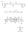
Fig. 2 is a five-side view of the power supply module illustrated inFig. 1 ; -
Fig. 3 is an exploded view of the power supply module illustrated inFig. 1 ; and -
Fig. 4 is a cross-sectional view illustrating a structure of a housing for electronic components, described in Japanese Unexamined Patent Application Publication No.2002-271064 - A power supply module according to an embodiment of the present invention will now be described.
- A configuration of a power supply module according to an embodiment will be described with reference to the drawings.
-
Fig. 1 is an outside perspective view of apower supply module 10 according to an embodiment.Fig. 2 is a five-side view of thepower supply module 10 illustrated inFig. 1 .Fig. 3 is an exploded view of thepower supply module 10 illustrated inFig. 1 . In the following description, the up-and-down direction inFig. 1 is simply referred to as an up-and-down direction. In plan view as viewed from above inFig. 1 , the direction in which shorter sides of thepower supply module 10 extend is defined as a front-and-back direction, and the direction in which longer sides of thepower supply module 10 extend is defined as a right-and-left direction. - The
power supply module 10 is a direct-current (DC) or alternating-current (AC) power supply circuit. As illustrated inFig. 1 to Fig. 3 , thepower supply module 10 includes aheatsink plate 12, acircuit board 14, and aheatsink sheet member 16. - The
circuit board 14 is a multilayered circuit board which is made of resin material and is substantially rectangular in plan view as viewed from above. Thecircuit board 14 has principal surfaces S1 and S2 and side surfaces S3 to S6. The principal surface S1 is a surface located on the upper side. The principal surface S2 is a surface located on the lower side. The side surface S3 is a surface located on the front side. The side surface S4 is a surface located on the right side. The side surface S5 is a surface located on the back side. The side surface S6 is a surface located on the left side. A circuit formed by conductors of copper or the like is disposed on the principal surfaces S1 and S2 and inside thecircuit board 14. - As illustrated in
Fig. 1 to Fig. 3 ,electronic components circuit board 14. As illustrated inFig. 2 andFig. 3 , a height h2 of theelectronic components 52a and 52b from the principal surface S1 in the up-and-down direction is smaller than a height h1 of theelectronic components 50a and 50b from the principal surface S1 in the up-and-down direction. - As illustrated in
Fig. 1 to Fig. 3 ,electronic components 54a, 54b, and 56a to 56c are mounted on the principal surface S2 of thecircuit board 14. As illustrated inFig. 2 andFig. 3 , a height h4 of the electronic components 56a to 56c from the principal surface S2 in the up-and-down direction is smaller than a height h3 of theelectronic component 54a and 54b from the principal surface S2 in the up-and-down direction. - The electronic components 50a and 54a face each other in the up-and-down direction, with the
circuit board 14 interposed therebetween, to form for example a ferrite core. Similarly, theelectronic components circuit board 14 interposed therebetween, to form for example a ferrite core. A choke coil or transformer is formed when such a ferrite core is configured to pass through a coil pattern in thecircuit board 14. Theelectronic component 52a and 52b are semiconductor devices. For example, theelectronic component 52a and 52b are switching devices, such as field-effect transistors (FETs). Theelectronic components 52a and 52b are devices that generate heat more easily than theelectronic components electronic components circuit board 14 form a power supply circuit. - The
circuit board 14 is provided withexternal connection terminals 30a to 30j protruding downward from the principal surface S2. As illustrated inFig. 2 , theexternal connection terminals 30a to 30e are aligned in this order from the front to the back, along the right (shorter) side of the principal surface S2. Also as illustrated inFig. 2 , theexternal connection terminals 30f to 30j are aligned in this order from the front to the back, along the left (shorter) side of the principal surface S2. - A height H2 indicates the height of the
external connection terminals 30a to 30j from the principal surface S2 in the up-and-down direction. Theexternal connection terminals 30a to 30j are stepped pins. As illustrated inFig. 2 , theexternal connection terminals 30a to 30j have each abase portion 60 and anend portion 62. For simplicity of the drawing, these reference numerals are given only to thebase portion 60 and theend portion 62 of theexternal connection terminal 30a inFig. 2 . Thebase portion 60 is the upper part of each of theexternal connection terminals 30a to 30j, and has a diameter greater than that of theend portion 62. A height H3 indicates the height of thebase portion 60 from the principal surface S2 in the up-and-down direction. Theend portion 62 is the lower part of each of theexternal connection terminals 30a to 30j, and has a diameter smaller than that of thebase portion 60. When thepower supply module 10 is mounted on another circuit board or apparatus, theend portions 62 are inserted into the circuit board or apparatus. However, thebase portions 60 are not inserted into the circuit board or apparatus in this case. Thus, when thepower supply module 10 is mounted on another circuit board or apparatus, thecircuit board 14 is held at the height H3 from the circuit board or apparatus. - The height H3 of the
base portions 60 from the principal surface S2 in the up-and-down direction is greater than the height h3 of theelectronic components 54a and 54b from the principal surface S2 in the up-and-down direction. Therefore, when thepower supply module 10 is mounted on another circuit board or apparatus, theelectronic components 54a and 54b can be prevented from coming into contact with the circuit board or apparatus. - The
heatsink plate 12 is formed by a single metal plate (aluminum plate). Theheatsink plate 12 has abody portion 20, fixing portions 22a to 22d, andbent portions 26a to 26d. - The
body portion 20 is a plate-like member located above thecircuit board 14 to face the principal surface S1. In plan view as viewed from above, thebody portion 20 is a substantially rectangular member having substantially the same size as thecircuit board 14. As illustrated inFig. 1 andFig. 3 , thebody portion 20 is provided with recessed portions G1 and G2 extending downward (or toward the circuit board 14). In plan view as viewed from above (in the direction of the normal to the principal surface S1), the recessed portions G1 and G2 overlap with theelectronic components 52a and 52b, respectively. It is preferable that the depth of the recessed portions G1 and G2 be substantially the same as the difference between the height h1 and the height h2. - The fixing portions 22a to 22d extend at an angle from the
body portion 20 to face the corresponding side surfaces S3 and S5. The fixing portions 22a to 22d then come into contact with the principal surface S2 to secure thebody portion 20 to thecircuit board 14. Specifically, the fixing portion 22a is a belt-like member extending in the up-and-down direction. The fixing portion 22a extends downward at an angle from thebody portion 20 at the left end of the front (longer) side of thebody portion 20. The fixing portion 22a faces thecircuit board 14 near the left end of the side surface S3 and extends to a position below thecircuit board 14. The fixing portion 22a is provided with a protrusion 24a at an end portion thereof extending below thecircuit board 14. The protrusion 24a protrudes backward from the fixing portion 22a. The protrusion 24a is in contact with the principal surface S2 near the left end of the front (longer) side of the principal surface S2. - The fixing
portion 22b is a belt-like member extending in the up-and-down direction. The fixingportion 22b extends downward at an angle from thebody portion 20 at the right end of the front (longer) side of thebody portion 20. The fixingportion 22b faces thecircuit board 14 near the right end of the side surface S3 and extends to a position below thecircuit board 14. The fixingportion 22b is provided with aprotrusion 24b at an end portion thereof extending below thecircuit board 14. Theprotrusion 24b protrudes backward from the fixingportion 22b. Theprotrusion 24b is in contact with the principal surface S2 near the right end of the front (longer) side of the principal surface S2. - The fixing
portion 22c is a belt-like member extending in the up-and-down direction. The fixingportion 22c extends downward at an angle from thebody portion 20 at the left end of the back (longer) side of thebody portion 20. The fixingportion 22c faces thecircuit board 14 near the left end of the side surface S5 and extends to a position below thecircuit board 14. Thus, the fixingportions 22a and 22c face each other in the front-and-back direction, with thecircuit board 14 interposed therebetween. The fixingportion 22c is provided with aprotrusion 24c at an end portion thereof extending below thecircuit board 14. Theprotrusion 24c protrudes forward from the fixingportion 22c. Theprotrusion 24c is in contact with the principal surface S2 near the left end of the back (longer) side of the principal surface S2. - The fixing
portion 22d is a belt-like member extending in the up-and-down direction. The fixingportion 22d extends downward at an angle from thebody portion 20 at the right end of the back (longer) side of thebody portion 20. The fixingportion 22d faces thecircuit board 14 near the right end of the side surface S5 and extends to a position below thecircuit board 14. Thus, the fixingportions circuit board 14 interposed therebetween. The fixingportion 22d is provided with aprotrusion 24d at an end portion thereof extending below thecircuit board 14. Theprotrusion 24d protrudes forward from the fixingportion 22d. Theprotrusion 24d is in contact with the principal surface S2 near the right end of the back (longer) side of the principal surface S2. Thus, the fixing portions 22a to 22d secure theheatsink plate 12 in place at the four corners of thecircuit board 14. - As illustrated in
Fig. 2 , a height H1 indicates the height of the fixing portions 22a to 22d from the principal surface S2 in the up-and-down direction. The height H1 is smaller than the height H2. Thus, since the lower ends of theend portions 62 of theexternal connection terminals 30a to 30j are located below the lower ends of the fixing portions 22a to 22d, theend portions 62 can be inserted into another circuit board or apparatus. The height H1 is preferably smaller than the height H3. Thus, when theentire end portions 62 are inserted into another circuit board or apparatus, the fixing portions 22a to 22d can be prevented from coming into contact with the circuit board or apparatus. - The
bent portions 26a to 26d extend at an angle from thebody portion 20 in the same direction as the fixing portions 22a to 22d (i.e., thebent portions 26a to 26d extend downward). Thebent portions 26a to 26d have a height smaller than that of the fixing portions 22a to 22d from thebody portion 20 in the up-and-down direction. Specifically, thebent portion 26a extends along the front (longer) side of thebody portion 20. Thebent portion 26a is connected, at both ends thereof in the right-and-left direction, to the fixingportions 22a and 22b. Thebent portion 26a does not face the side surface S3 of thecircuit board 14. Thus, thebent portion 26a is separated by a gap from thecircuit board 14. - The
bent portion 26b extends along the right (shorter) side of thebody portion 20. Thebent portion 26b does not face the side surface S4 of thecircuit board 14. Thus, thebent portion 26b is separated by a gap from thecircuit board 14. - The
bent portion 26c extends along the back (longer) side of thebody portion 20. Thebent portion 26c is connected, at both ends thereof in the right-and-left direction, to the fixingportions bent portion 26c does not face the side surface S5 of thecircuit board 14. Thus, thebent portion 26c is separated by a gap from thecircuit board 14. - The
bent portion 26d extends along the left (shorter) side of thebody portion 20. Thebent portion 26d does not face the side surface S6 of thecircuit board 14. Thus, thebent portion 26d is separated by a gap from thecircuit board 14. - The
heatsink plate 12 is formed by die-cutting, bending, and press working a single metal plate. Specifically, the fixing portions 22a to 22d and thebent portions 26a to 26d are formed by bending, and the protrusions 24a to 24d and the recessed portions G1 and G2 are formed by press working. - As illustrated in
Fig. 3 , theheatsink sheet member 16 is interposed between the principal surface S1 and thebody portion 20. Theheatsink sheet member 16 is in contact with theelectronic components body portion 20. Theheatsink sheet member 16 is made of material having good heat dissipation properties. For example, theheatsink sheet member 16 is made of a silicone compound. Theheatsink sheet member 16 preferably has elasticity. - The
power supply module 10 configured as described above includes fewer components. Specifically, theheatsink plate 12 extends downward at an angle from thebody portion 20 to face the side surfaces S3 and S5 and come into contact with the principal surface S2. Thus, theheatsink plate 12 is secured to thecircuit board 14. Theheatsink plate 12 of thepower supply module 10 is composed of a single component. This means that thepower supply module 10 includes fewer components than thehousing 500 described in Japanese Unexamined Patent Application Publication No.2002-271064 - In the
power supply module 10, theheatsink plate 12 is secured to thecircuit board 14 by the fixing portions 22a to 22d that form part of theheatsink plate 12. Therefore, thepower supply module 10 does not require any screws or fittings for securing theheatsink plate 12 to thecircuit board 14. This means again that thepower supply module 10 includes fewer components. - In the
power supply module 10, theheatsink plate 12 is formed by bending and press working a single metal plate. A mold used for bending and press working is less costly than that for casting. Therefore, the cost of producing theheatsink plate 12 is lower than that of producing a heatsink plate by casting. - The
power supply module 10 can achieve a high heat dissipation effect. Specifically, thebody portion 20 is provided with the recessed portions G1 and G2 extending toward thecircuit board 14. In plan view as viewed from above, the recessed portions G1 and G2 overlap with theelectronic components 52a and 52b, respectively, having the height h2 smaller than the height h1 of theelectronic components 50a and 50b. This reduces the distance between thebody portion 20 and theelectronic components 52a and 52b. Thus, heat generated by theelectronic components 52a and 52b is efficiently transferred via theheatsink sheet member 16 to thebody portion 20. With the recessed portions G1 and G2 of thebody portion 20, the distance between thebody portion 20 and theelectronic components 52a and 52b is close to that between thebody portion 20 and theelectronic components 50a and 50b. This means that the magnitude of force applied from theelectronic components 52a and 52b to thebody portion 20 is close to that applied from theelectronic components 50a and 50b to thebody portion 20. It is thus possible to reduce concentration of stress on part of thebody portion 20. - The height H1 of the fixing portions 22a to 22d from the principal surface S2 in the up-and-down direction is smaller than the height H2. Thus, since the lower ends of the
end portions 62 of theexternal connection terminals 30a to 30j are located below the lower ends of the fixing portions 22a to 22d, theend portions 62 can be inserted into another circuit board or apparatus. The height H1 is smaller than the height H3 of thebase portions 60 of theexternal connection terminals 30a to 30j from the principal surface S2 in the up-and-down direction. Thus, when theentire end portions 62 are inserted into another circuit board or apparatus, the fixing portions 22a to 22d can be prevented from coming into contact with the circuit board or apparatus. - The
heatsink plate 12 has thebent portions 26a to 26d extending at an angle from thebody portion 20 in the same direction as the fixing portions 22a to 22d. Since this increases the moment of inertia of area of thebody portion 20, the strength of thebody portion 20 is improved. As described above, thebent portions - As illustrated in
Fig. 3 , theheatsink sheet member 16 is interposed between the principal surface S1 and thebody portion 20 and is in contact with theelectronic components body portion 20. Thus, heat generated by theelectronic components heatsink sheet member 16 to thebody portion 20. This improves the heat dissipation properties of thepower supply module 10. - The
heatsink sheet member 16 has elasticity. Thus, theheatsink sheet member 16 presses thebody portion 20 and thecircuit board 14 upward and downward, respectively. Since this causes the protrusions 24a to 24d to be firmly pressed against thecircuit board 14, it is possible to reduce looseness of thecircuit board 14 in the up-and-down direction with respect to theheatsink plate 12. With theheatsink sheet member 16 having elasticity, theelectronic components body portion 20. Thus, since a force applied from theelectronic components body portion 20 is distributed by theheatsink sheet member 16 over theentire body portion 20, it is possible to reduce concentration of stress on part of thebody portion 20. - The
heatsink plate 12 is formed by bending and press working a single metal plate. For better workability, a thin metal plate is used to make theheatsink plate 12. Therefore, thepower supply module 10 is lighter in weight and lower in profile than a power supply module that includes a heatsink plate produced by casting. - The power supply module according to the present invention is not limited to the
power supply module 10 of the embodiment described above, and may be changed within the scope of the present invention. - In the
power supply module 10, the fixing portions 22a to 22d have the protrusions 24a to 24d formed by press working. The protrusions 24a to 24d are in contact with the principal surface S2 of thecircuit board 14 to secure theheatsink plate 12 to thecircuit board 14. However, theheatsink plate 12 may be secured to thecircuit board 14 in other ways. For example, the fixingportions 22a and 22b may be bent backward at the lower ends thereof to come into contact with the principal surface S2, and the fixingportions heatsink plate 12 is more firmly secured to thecircuit board 14. - Note that although bending the fixing portions 22a to 22d increases the contact area where the fixing portions 22a to 22d are in contact with the principal surface S2, this results in a decrease in area for mounting electronic components on the principal surface S2. To allow mounting of more electronic components, it is preferable to use the protrusions 24a to 24d described above.
- Although the
circuit board 14 and thebody portion 20 are substantially rectangular in plan view as viewed from above, their shape is not limited to this. - The positions where the fixing portions 22a to 22d are in contact with the principal surface S2 of the
circuit board 14 are not limited to the four corners of the principal surface S2. The fixing portions 22a to 22d may be in contact with the principal surface S2 at any positions, as long as the fixing portions 22a to 22d can secure theheatsink plate 12 to thecircuit board 14. For the fixing portions 22a to 22d to secure theheatsink plate 12 to thecircuit board 14, it is only necessary that two of the fixing portions 22a to 22d be disposed to face one side surface of thecircuit board 14 and that the other two of the fixing portions 22a to 22d be disposed to face the opposite side surface of thecircuit board 14. Thus, thecircuit board 14 is sandwiched between the fixing portions 22a to 22d. - The present invention is useful when applied to power supply modules, and particularly advantageous in that it can reduce the number of components of such power supply modules.
- While preferred embodiments of the invention have been described above, it is to be understood that variations and modifications will be apparent to those skilled in the art without departing from the scope and spirit of the invention. The scope of the invention, therefore, is to be determined solely by the following claims.
Claims (11)
- A power supply module comprising:a circuit board having a first principal surface, a second principal surface, and side surfaces, the circuit board having electronic components mounted on the first principal surface; anda heatsink plate having a plate-like body portion that faces the first principal surface and a plurality of fixing portions that extend at an angle from the body portion to face the side surfaces, the fixing portions being configured to come into contact with the second principal surface to secure the body portion to the circuit board.
- The power supply module according to Claim 1,
wherein the heatsink plate is formed by a single metal plate. - The power supply module according to Claim 1 or 2,
wherein the fixing portions are each provided with a protrusion in contact with the second principal surface. - The power supply module according to any one of Claims 1 to 3, wherein the body portion is provided with a recessed portion extending toward the circuit board.
- The power supply module according to Claim 4,
wherein the electronic components include a first electronic component and a second electronic component;
a height of the second electronic component from the first principal surface is smaller than a height of the first electronic component from the first principal surface; and
the recessed portion overlaps with the second electronic component in plan view in the direction of the normal to the first principal surface. - The power supply module according to Claim 5,
wherein the second electronic component is a semiconductor device. - The power supply module according to any one of Claims 1 to 6, wherein the heatsink plate is formed by bending and press working.
- The power supply module according to any one of Claims 1 to 7, wherein the circuit board is provided with a plurality of external connection terminals protruding from the second principal surface; and
a height of the external connection terminals from the second principal surface is greater than a height of the fixing portions from the second principal surface. - The power supply module according to any one of Claims 1 to 8, wherein the heatsink plate has a plurality of bent portions extending at an angle from the body portion in the same direction as the fixing portions, the bent portions having a height smaller than a height of the fixing portions from the body portion.
- The power supply module according to any one of Claims 1 to 9, further comprising a sheet member between the first principal surface and the body portion.
- The power supply module according to Claim 10, wherein the sheet member has elasticity.
Applications Claiming Priority (1)
| Application Number | Priority Date | Filing Date | Title |
|---|---|---|---|
| JP2012088342A JP5733260B2 (en) | 2012-04-09 | 2012-04-09 | Power module |
Publications (2)
| Publication Number | Publication Date |
|---|---|
| EP2651203A2 true EP2651203A2 (en) | 2013-10-16 |
| EP2651203A3 EP2651203A3 (en) | 2017-03-08 |
Family
ID=48044664
Family Applications (1)
| Application Number | Title | Priority Date | Filing Date |
|---|---|---|---|
| EP13162051.0A Withdrawn EP2651203A3 (en) | 2012-04-09 | 2013-04-03 | Power supply module |
Country Status (4)
| Country | Link |
|---|---|
| US (1) | US9553428B2 (en) |
| EP (1) | EP2651203A3 (en) |
| JP (1) | JP5733260B2 (en) |
| CN (1) | CN103369929B (en) |
Families Citing this family (3)
| Publication number | Priority date | Publication date | Assignee | Title |
|---|---|---|---|---|
| US10103801B2 (en) | 2015-06-03 | 2018-10-16 | At&T Intellectual Property I, L.P. | Host node device and methods for use therewith |
| CN105374769A (en) * | 2015-12-04 | 2016-03-02 | 重庆臻远电气有限公司 | Heat radiation apparatus |
| KR102924577B1 (en) * | 2020-01-06 | 2026-02-05 | 엘지전자 주식회사 | Converter |
Citations (3)
| Publication number | Priority date | Publication date | Assignee | Title |
|---|---|---|---|---|
| JPH11163566A (en) * | 1997-11-28 | 1999-06-18 | Sony Corp | Heat dissipation structure of electronic equipment |
| JP2002271064A (en) | 2001-03-12 | 2002-09-20 | Denso Corp | Electronic component storage case |
| US20080106884A1 (en) * | 2006-11-03 | 2008-05-08 | Gerald Robert English | Snap install emi shields with protrusions and electrically-conductive members for attachment to substrates |
Family Cites Families (13)
| Publication number | Priority date | Publication date | Assignee | Title |
|---|---|---|---|---|
| US4218578A (en) * | 1978-08-04 | 1980-08-19 | Burr-Brown Research Corp. | RF Shield for an electronic component |
| US7082033B1 (en) | 1998-02-13 | 2006-07-25 | Micron Technology, Inc. | Removing heat from integrated circuit devices mounted on a support structure |
| US5959842A (en) * | 1998-05-14 | 1999-09-28 | Lucent Technologies Inc. | Surface mount power supply package and method of manufacture thereof |
| JP4300706B2 (en) * | 2000-12-21 | 2009-07-22 | ソニー株式会社 | Heat dissipation device for electronic equipment |
| JP2006303374A (en) | 2005-04-25 | 2006-11-02 | Mitsumi Electric Co Ltd | Heat dissipation device in electronic equipment |
| CN100463594C (en) * | 2005-06-18 | 2009-02-18 | 鸿富锦精密工业(深圳)有限公司 | Electromagnetic shielding device with heat dissipation function |
| US20080128897A1 (en) * | 2006-12-05 | 2008-06-05 | Tong Wa Chao | Heat spreader for a multi-chip package |
| WO2010067725A1 (en) * | 2008-12-12 | 2010-06-17 | 株式会社 村田製作所 | Circuit module |
| DE102009054517B4 (en) * | 2009-12-10 | 2011-12-29 | Robert Bosch Gmbh | Electronic control unit |
| JP2011176096A (en) | 2010-02-24 | 2011-09-08 | Mitsumi Electric Co Ltd | Electronic apparatus |
| WO2011148665A1 (en) | 2010-05-24 | 2011-12-01 | シャープ株式会社 | Heat dissipation structure for electronic equipment |
| CN102906870A (en) | 2010-06-18 | 2013-01-30 | 夏普株式会社 | Heat dissipation structure of electronic equipment |
| JP5351107B2 (en) * | 2010-07-23 | 2013-11-27 | 三菱電機株式会社 | Capacitor cooling structure and inverter device |
-
2012
- 2012-04-09 JP JP2012088342A patent/JP5733260B2/en active Active
-
2013
- 2013-03-28 US US13/851,986 patent/US9553428B2/en active Active
- 2013-04-03 EP EP13162051.0A patent/EP2651203A3/en not_active Withdrawn
- 2013-04-03 CN CN201310114495.6A patent/CN103369929B/en active Active
Patent Citations (3)
| Publication number | Priority date | Publication date | Assignee | Title |
|---|---|---|---|---|
| JPH11163566A (en) * | 1997-11-28 | 1999-06-18 | Sony Corp | Heat dissipation structure of electronic equipment |
| JP2002271064A (en) | 2001-03-12 | 2002-09-20 | Denso Corp | Electronic component storage case |
| US20080106884A1 (en) * | 2006-11-03 | 2008-05-08 | Gerald Robert English | Snap install emi shields with protrusions and electrically-conductive members for attachment to substrates |
Also Published As
| Publication number | Publication date |
|---|---|
| JP5733260B2 (en) | 2015-06-10 |
| EP2651203A3 (en) | 2017-03-08 |
| US20130265723A1 (en) | 2013-10-10 |
| CN103369929B (en) | 2016-08-03 |
| JP2013219169A (en) | 2013-10-24 |
| US9553428B2 (en) | 2017-01-24 |
| CN103369929A (en) | 2013-10-23 |
Similar Documents
| Publication | Publication Date | Title |
|---|---|---|
| JP4609504B2 (en) | Electronics | |
| US20150373836A1 (en) | Semiconductor device | |
| JP6719021B2 (en) | Power converter | |
| CN110914936A (en) | Circuit structure | |
| JP2016015822A (en) | Electrical junction box | |
| US9204572B2 (en) | Heat radiation arrangement | |
| WO2020059615A1 (en) | Electric compressor | |
| JP2014090523A (en) | Switching power supply device | |
| US10342152B2 (en) | Electronic device having a housing with a circuit board provided therein | |
| US20190123539A1 (en) | Substrate unit | |
| CN107210592B (en) | Circuit structure | |
| EP2651203A2 (en) | Power supply module | |
| US9030811B2 (en) | Electronic device chassis and electronic device | |
| US20180033714A1 (en) | Substrate unit | |
| CN104918457B (en) | Electronic equipment | |
| JP6402280B2 (en) | Electronics | |
| JP2014183719A (en) | Member for holding distance between substrates, and inverter device | |
| CN108432113A (en) | DC/DC converters | |
| US11343913B2 (en) | Circuit board structure | |
| JP5892691B2 (en) | Electronic equipment | |
| JP6454051B2 (en) | Electronics | |
| JP5777175B2 (en) | Electronic circuit board and its assembly method | |
| JP2008103577A (en) | Power module heat dissipation structure and motor control device including the same | |
| JP4428092B2 (en) | Electronic component mounting method | |
| KR101736500B1 (en) | Circuit components and Switching Mode Power Supply having the same |
Legal Events
| Date | Code | Title | Description |
|---|---|---|---|
| PUAI | Public reference made under article 153(3) epc to a published international application that has entered the european phase |
Free format text: ORIGINAL CODE: 0009012 |
|
| 17P | Request for examination filed |
Effective date: 20130403 |
|
| AK | Designated contracting states |
Kind code of ref document: A2 Designated state(s): AL AT BE BG CH CY CZ DE DK EE ES FI FR GB GR HR HU IE IS IT LI LT LU LV MC MK MT NL NO PL PT RO RS SE SI SK SM TR |
|
| AX | Request for extension of the european patent |
Extension state: BA ME |
|
| PUAL | Search report despatched |
Free format text: ORIGINAL CODE: 0009013 |
|
| AK | Designated contracting states |
Kind code of ref document: A3 Designated state(s): AL AT BE BG CH CY CZ DE DK EE ES FI FR GB GR HR HU IE IS IT LI LT LU LV MC MK MT NL NO PL PT RO RS SE SI SK SM TR |
|
| AX | Request for extension of the european patent |
Extension state: BA ME |
|
| RIC1 | Information provided on ipc code assigned before grant |
Ipc: H05K 7/14 20060101AFI20170202BHEP Ipc: H05K 7/20 20060101ALI20170202BHEP Ipc: H02B 1/56 20060101ALI20170202BHEP |
|
| 17Q | First examination report despatched |
Effective date: 20200520 |
|
| STAA | Information on the status of an ep patent application or granted ep patent |
Free format text: STATUS: THE APPLICATION IS DEEMED TO BE WITHDRAWN |
|
| 18D | Application deemed to be withdrawn |
Effective date: 20201001 |