EP2648328A2 - Protection d'un convertisseur de courant avec circuit intermédiaire contre les dommages causés par la contre-tension d'une machine synchrone - Google Patents
Protection d'un convertisseur de courant avec circuit intermédiaire contre les dommages causés par la contre-tension d'une machine synchrone Download PDFInfo
- Publication number
- EP2648328A2 EP2648328A2 EP13154366.2A EP13154366A EP2648328A2 EP 2648328 A2 EP2648328 A2 EP 2648328A2 EP 13154366 A EP13154366 A EP 13154366A EP 2648328 A2 EP2648328 A2 EP 2648328A2
- Authority
- EP
- European Patent Office
- Prior art keywords
- bot
- voltage
- circuit
- primary
- switches
- Prior art date
- Legal status (The legal status is an assumption and is not a legal conclusion. Google has not performed a legal analysis and makes no representation as to the accuracy of the status listed.)
- Granted
Links
- 230000001360 synchronised effect Effects 0.000 title claims description 25
- 230000006378 damage Effects 0.000 title description 8
- 238000000034 method Methods 0.000 claims abstract description 18
- 230000005284 excitation Effects 0.000 claims description 7
- 230000000903 blocking effect Effects 0.000 claims description 4
- 239000003990 capacitor Substances 0.000 description 6
- 238000002955 isolation Methods 0.000 description 6
- 230000003313 weakening effect Effects 0.000 description 6
- 238000000926 separation method Methods 0.000 description 5
- 238000004804 winding Methods 0.000 description 4
- 230000005540 biological transmission Effects 0.000 description 3
- 238000005516 engineering process Methods 0.000 description 3
- 230000005669 field effect Effects 0.000 description 3
- 238000009499 grossing Methods 0.000 description 3
- 229910044991 metal oxide Inorganic materials 0.000 description 2
- 150000004706 metal oxides Chemical class 0.000 description 2
- 230000004913 activation Effects 0.000 description 1
- 230000006978 adaptation Effects 0.000 description 1
- 238000006243 chemical reaction Methods 0.000 description 1
- 238000010276 construction Methods 0.000 description 1
- 230000000254 damaging effect Effects 0.000 description 1
- 230000001419 dependent effect Effects 0.000 description 1
- 239000000446 fuel Substances 0.000 description 1
- 229910052987 metal hydride Inorganic materials 0.000 description 1
- 238000012544 monitoring process Methods 0.000 description 1
- 230000008569 process Effects 0.000 description 1
- 230000001960 triggered effect Effects 0.000 description 1
Images
Classifications
-
- H—ELECTRICITY
- H02—GENERATION; CONVERSION OR DISTRIBUTION OF ELECTRIC POWER
- H02M—APPARATUS FOR CONVERSION BETWEEN AC AND AC, BETWEEN AC AND DC, OR BETWEEN DC AND DC, AND FOR USE WITH MAINS OR SIMILAR POWER SUPPLY SYSTEMS; CONVERSION OF DC OR AC INPUT POWER INTO SURGE OUTPUT POWER; CONTROL OR REGULATION THEREOF
- H02M1/00—Details of apparatus for conversion
- H02M1/32—Means for protecting converters other than automatic disconnection
-
- H—ELECTRICITY
- H02—GENERATION; CONVERSION OR DISTRIBUTION OF ELECTRIC POWER
- H02M—APPARATUS FOR CONVERSION BETWEEN AC AND AC, BETWEEN AC AND DC, OR BETWEEN DC AND DC, AND FOR USE WITH MAINS OR SIMILAR POWER SUPPLY SYSTEMS; CONVERSION OF DC OR AC INPUT POWER INTO SURGE OUTPUT POWER; CONTROL OR REGULATION THEREOF
- H02M7/00—Conversion of ac power input into dc power output; Conversion of dc power input into ac power output
- H02M7/42—Conversion of dc power input into ac power output without possibility of reversal
- H02M7/44—Conversion of dc power input into ac power output without possibility of reversal by static converters
- H02M7/48—Conversion of dc power input into ac power output without possibility of reversal by static converters using discharge tubes with control electrode or semiconductor devices with control electrode
Definitions
- the present invention is in the field of power electronics and relates to a power converter with a voltage intermediate circuit, and a method for operating such a power converter.
- Power converters typically include a bridge circuit having a plurality of parallel half-bridges for generating the alternating current phases.
- a voltage intermediate circuit with a capacitor assembly is provided as charge storage for supplying the bridge circuit, whereby a voltage support and smoothing for the operation of the electrical machine can be achieved.
- a half-bridge two power switches with their power or load current paths are arranged in a series circuit, with a freewheeling diode usually being arranged in antiparallel to the circuit breakers. It is known to design such a circuit breaker by one or more power transistors connected in parallel.
- each half-bridge comprises a first power switch (“TOP switch” or “high-side switch”), which is connected with its load current connections between a first supply potential terminal and a load output, and a second power switch (“BOT switch” or “Low -Side switch “), which is interconnected with its load current connections between the load output and a second supply potential connection.
- the load output of the half-bridge can be connected to an electrical load, for example the winding of a synchronous machine, get connected.
- the first supply potential connection is connected to the upper potential of the intermediate circuit voltage
- the second supply potential connection to the lower potential of the intermediate circuit voltage so that the load output of the half bridge designed as a center tap can be selectively connected to the upper or lower potential of the intermediate circuit voltage
- a control of the bridge circuit is effected by a control circuit, which is typically divided into a primary-side circuit part (low-voltage side) and a secondary-side circuit part (high-voltage side), which are electrically isolated, but interconnected circuit technology.
- the primary-side circuit part of the control circuit is connected to a higher-level control device, for example an engine control unit of a motor vehicle, while the secondary-side circuit part is connected directly to the power switches and controls them.
- a supply of the primary-side circuit part of the control circuit is effected by one or more primary-side operating voltages, which are typically in the range of 1 to 24 volts and are generated in motor vehicles usually from the on-board voltage (for example 12 or 24 volts).
- the secondary-side circuit part of the control circuit is at high voltage potential, for example 600 to 900 volts.
- a galvanic separation of the two circuit parts can be done for example by optocouplers, pulse transformer or by integrated circuit technology, which is known in the art per se.
- Synchronous machines with permanent magnetic field excitation which are supplied with an operating voltage by a 3-phase inverter, are frequently used for the electric drive of motor vehicles.
- Such synchronous machines are also operated in a speed range above the rated speed, but this requires a speed-dependent adaptation of the field current component of the phase current introduced into the windings to a damaging effect of the counter-voltage generated in the synchronous machine (Polradschreib), which is fed via the freewheeling diodes in the intermediate circuit , to avoid.
- a so-called "field weakening current” is generated by the 3-phase inverter.
- the object of the present invention is to develop conventional power converter with voltage intermediate circuit so that when feeding running in field weakening synchronous machines with permanent magnetic field excitation in case of failure of the primary-side operating voltages damage to the converter is reliably and reliably avoided by the reverse voltage generated in the synchronous machine ,
- power converter refers to devices known per se for the conversion of electrical energy. Converters in this sense are in particular multiphase DC / AC converters (DC / AC converters) or inverters.
- the power converter according to the invention comprises a voltage intermediate circuit for providing an intermediate circuit voltage (DC voltage), to which a plurality of parallel half bridges with TOP and BOT switches is connected.
- DC voltage intermediate circuit voltage
- two circuit breakers are arranged with their load current paths in a half-bridge in a series circuit, wherein a first circuit breaker or TOP switch with its load current input to a first intermediate circuit line for an upper potential (DC +) and a second power switch or BOT switch with his Load current output connected to a second DC link for a lower potential (DC-) of the intermediate circuit voltage is.
- a center tap between the TOP and BOT switches forms a load output of the half-bridge for connecting the generated AC phase to an electrical load.
- the circuit breakers are typically designed to carry electrical currents of several hundred amps and block voltages up to about 1000 volts.
- bipolar transistors with insulated gate electrode (IBGT) with a collector electrode as load current input, an emitter electrode as load current output and a gate electrode as control input, or field effect transistors (FET), in particular metal oxide field effect transistors (MOSFET), are usually used.
- FET field effect transistors
- MOSFET metal oxide field effect transistors
- the power converter according to the invention further comprises a control circuit for controlling the power switch, which is divided into a primary-side circuit part and a secondary-side circuit part, the primary-side circuit part (low-voltage side) and the secondary-side circuit part (high-voltage side) by a galvanically isolating transmission device electrically isolated, but interconnected circuit technology are.
- the primary side circuit part includes a primary side power supply for generating one or more typically a plurality of primary side operating voltages (e.g., logic voltages) for supplying the primary side circuit part.
- the primary-side power supply is typically powered by the on-board voltage (e.g., 12 or 24 volts) as an input voltage.
- the primary-side operating voltages generated from the input voltage are typically smaller than the input voltage, but the input voltage itself may also be provided as the primary-side operating voltage.
- the primary-side operating voltages are typically in the range of 1 to 24 volts.
- the primary-side circuit part further comprises a test element, which is designed to check the presence of predetermined or predefinable setpoint values of the primary-side operating voltages and to output an error signal on the basis of this test (test result).
- the error signal includes two signal or logic levels, ie, a high logic level (high) and a low logic level (low), for example, the error signal having a high logic level when the primary side operating voltages have their setpoints, or a low logic level, if at least a primary-side operating voltage deviates from the nominal value.
- the secondary-side circuit part comprises a TOP drive circuit controllable by TOP control signals for generating control voltages for switching the TOP switches and a BOT drive circuit controllable by BOT control signals for generating control voltages for switching the BOT switches.
- the secondary-side circuit part further comprises a safety or additional circuit with a programmable (eg microprocessor-based) control logic module connected to the BOT driver circuit, which is designed to output a BOT driver signal on the basis of the error signal as an output signal to the BOT driver circuit in which all BOT switches are simultaneously closed or brought into the ON state by the BOT drive signal in order to short-circuit the load outputs of the half bridges if at least one primary-side operating voltage deviates from the nominal value.
- the control logic module is coupled to the test member such that the error signal is present as an input signal to the control logic module.
- the term "turn-on” in the context of a power switch refers to the switching of the power switch to its on-state in which the power or load current path is electrically conductive.
- the term “turn-off” refers to switching the circuit breaker to its off-state, in which the power or load current path is electrically insulating.
- the secondary-side circuit part further comprises a secondary-side voltage supply device for generating at least one secondary-side operating voltage for supplying the BOT driver circuit and the additional circuit, in particular the control logic module.
- the secondary-side voltage supply device is coupled to at least one primary-side operating voltage so that in the event of a failure of at least one primary-side operating voltage, as a rule, the at least one secondary-side operating voltage also fails.
- the secondary-side circuit part further comprises a DC / DC converter (DC / DC converter) for converting the intermediate circuit voltage into a secondary-side backup voltage for supplying the BOT driver circuit and the additional circuit, in particular the control logic module, in case of failure of the secondary-side operating voltage.
- the DC / DC converter is electrically connected for this purpose with the BOT driver circuit and the additional circuit. This can be realized, for example be that two voltage outputs of the DC / DC converter for providing the equivalent voltage with two voltage outputs of the secondary-side power supply device for providing the secondary-side operating voltage are electrically connected.
- the backup voltage is preferably provided simultaneously with the secondary operating voltage so that it is immediately available if the secondary operating voltage fails.
- the power converter according to the invention thus takes place in case of failure in case of failure of one or more primary-side operating voltages, which usually also has the failure of the secondary side operating voltage result, a substitute supply of the BOT driver circuit and the additional circuit, in particular control logic module, through which from the intermediate circuit voltage generated equivalent voltage.
- all BOT switches are switched on at the same time, so that the load outputs of the half bridges are short-circuited.
- the converter according to the invention and the synchronous machine can thus be converted into a safe operating state in the event of a fault in which at least one primary-side operating voltage has failed.
- the DC / DC converter is designed to generate a substitute voltage which is smaller than the secondary-side operating voltage.
- the primary-side circuit part comprises a programmable (for example microprocessor-based) safety logic component connected to the test member for forwarding the TOP control signals and BOT control signals to the TOP or BOT driver circuit.
- the error signal generated by the test element is applied to the safety logic module as an input signal.
- the safety logic module is designed to block forwarding of the TOP and BOT control signals on the basis of the error signal if at least one primary-side operating voltage deviates from the nominal value.
- the TOP and BOT control signals are passed on unhindered to the TOP or BOT driver circuit, while if an error signal with a low logic level (at least one primary-side operating voltage deviates from the nominal value) a forwarding of the TOP and BOT control signals is blocked by the safety logic module.
- the safety logic module By this measure can be achieved in a particularly advantageous manner that in the event of an error inadvertent switching on or off of the TOP switch and / or BOT switch is avoided by the TOP and BOT control signals.
- the TOP switches in the absence of control voltage in the blocking state, so that in particular a short circuit in the DC voltage circuit can be avoided by this measure.
- only the secondary-side BOT driver signal generated in a defined manner serves to control the BOT switches. The reliability of the converter can be further improved.
- the test member comprises a window comparator for each primary-side operating voltage, by which it can be checked whether the primary-side operating voltage is within a predefinable setpoint range.
- the voltage outputs of the DC / DC converter are electrically connected to the voltage outputs of the secondary-side power supply device with the interposition of a diode.
- the diode is arranged so that a current flow in the direction of the DC / DC converter is blocked, so that advantageously only current can flow from the DC / DC converter to the logic components to be supplied.
- the BOT driver circuit comprises an OR gate for each BOT switch, which is used to control a power amplifier for generating a control voltage for the BOT switch.
- the OR gate is supplied with the BOT control signals as the first input signal and the BOT drive signal as the second input signal.
- control logic module is connected to an analog / digital converter connected to the equivalent voltage, wherein an output voltage of the analog / digital converter based on the equivalent voltage is applied to the control logic module.
- This measure advantageously makes it possible to check the substitute voltage by the control logic module, wherein the BOT switch signal can be prevented from being turned on by the BOT driver signal if a suitable substitute voltage is not present.
- a BOT drive signal having a logic level (e.g., logic low) not turning on the BOT switches is output if the backup voltage falls below a predetermined voltage level.
- control logic module is set up so that switching on the BOT switch only after a predetermined delay time after switching off the TOP switch (for example, by blocking the TOP control signals).
- the control logic module is set up such that the BOT switch is only switched on by the BOT driver signal above a specifiable upper limit value for the intermediate circuit voltage.
- the invention further extends to a synchronous machine with permanent magnetic field excitation, which comprises a power converter as described above for supplying a multi-phase operating voltage.
- the invention extends to a motor vehicle with an electric or hybrid drive, which is equipped with such a synchronous machine as a drive machine.
- the invention extends to a method for operating a power converter.
- the power converter comprises a voltage intermediate circuit for providing an intermediate circuit voltage, to which a plurality of parallel half bridges with TOP and BOT switches is connected, and a control circuit for the power switch, which is divided into a primary-side circuit part and a secondary-side circuit part, wherein the secondary-side circuit part a TOP driver circuit for controlling the TOP switch and a BOT driver circuit for controlling the BOT switch comprises.
- the power converter can be designed in particular as described according to the invention.
- the method comprises the following steps: generating one or more primary-side operating voltages for supplying voltage to the primary-side circuit part; Checking the presence of predeterminable setpoint values of the primary-side operating voltages and generating an error signal; Generating a BOT driver signal based on the error signal by a secondary-side additional circuit and turning on all BOT switches by the BOT driver signal, if at least one primary-side operating voltage deviates from the desired value; Generating at least one secondary-side operating voltage for supplying the BOT driver circuit and additional circuit; Converting the intermediate circuit voltage into a substitute voltage for replacement power supply of the BOT driver circuit and additional circuit in case of failure of the secondary-side operating voltage.
- a substitute voltage is generated which is smaller than the secondary-side operating voltage.
- the BOT switches are turned on only after expiry of a predeterminable delay time after turning off the TOP switch.
- the BOT switches are switched on only above a predefinable upper limit value for the intermediate voltage of the voltage intermediate circuit and / or the switched BOT switches are switched off below a predefinable lower limit value for the intermediate voltage of the voltage intermediate circuit by the BOT drive signal.
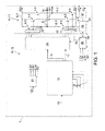
- Fig. 1 Be first Fig. 1 considered, which is illustrated with reference to a schematic representation of the structure of an embodiment of a generally designated by the reference numeral 1, the inventive 3-phase inverter.
- the 3-phase inverter 1 is used to convert a DC voltage into three AC phases for feeding an electrical load, here for example a permanent-magnet synchronous machine of a motor vehicle with electric or hybrid drive, which in Fig. 1 not shown in detail.
- the 3-phase inverter 1 comprises a bridge circuit 2 with three parallel half-bridges 3, which each serve to generate an alternating current phase.
- Each half-bridge 3 has, in a manner known per se, a switch pair of two power switches 4 connected in series with their load current paths and designed as power transistors, for example bipolar power transistors with insulated gate electrode (IGBT) or metal oxide field effect transistors (MOSFET).
- IGBT insulated gate electrode
- MOSFET metal oxide field effect transistors
- Each circuit breaker 4, a freewheeling diode is connected in parallel with the opposite direction of passage, which in Fig. 1 not shown.
- Each power switch 4 can be realized by one or more power transistors connected in parallel.
- the bridge circuit 2 is connected to the DC voltage of a voltage intermediate circuit 6, for which purpose the half-bridges 3 are electrically connected to two intermediate circuit lines 7, 7 '.
- the voltage intermediate circuit 6 includes an in Fig. 1 not shown condenser assembly for charge storage, which is connected to the DC link lines 7, 7 'so that a first DC link 7, an upper or higher potential (DC +) and a second DC link 7' serving as a reference potential, lower or lower potential (DC -) having. From the difference between the two potentials (DC +, DC-) results in the intermediate circuit voltage, which is converted by the half-bridges 3 to the AC phases.
- Each half-bridge 3 comprises a TOP switch 8, which with its load current connections between a connection point not designated in more detail with the first intermediate circuit line 7 and a trained as a center tap load output 10 is connected, and a BOT switch 9, which is connected with its load current terminals between the load output 10 and a connection point unspecified with the second DC link 7 '.
- the load output 10 of a half-bridge 3 is electrically connected to a connection point 5 between two series-connected circuit breakers 4 of a same half-bridge 3.
- AC phases can be generated, here referred to in common terminology with u, v, w.
- the AC phases may be connected to an electrical load, here for example the winding strands (not shown) of the synchronous machine.
- the winding strands can each be subjected to a potential of predetermined polarity and size for a certain period of time.
- the DC link voltage In order to generate sufficient for the operation of the motor vehicle drive power, the DC link voltage must be sufficiently large.
- the DC link voltage is in the range of 600-900 volts.
- the capacitance of the capacitor assembly is, for example, 1000 ⁇ F.
- the capacitor module can be electrically charged by a DC power source (not shown) connected to the two DC link lines 7, 7 ', for example an accumulator or a fuel cell. If the DC power source is simultaneously designed as a DC sink (accumulator), a charge can also occur during a braking operation of the motor vehicle, the synchronous machine acts as a generator and the generated 3-phase AC voltage is converted by the bridge circuit 2 into a DC voltage.
- the accumulator is designed as a nickel-metal hydride accumulator with an operating voltage in the range of 100 to 600 volts.
- a control circuit 11 of the 3-phase inverter 1 In order to generate the alternating current phases u, v, w at the load outputs 10, the power switches 4 of the bridge circuit 2 must be controlled accordingly by a control circuit 11 of the 3-phase inverter 1.
- the control circuit 11 is divided in a conventional manner into a primary-side circuit part 12 and a secondary-side circuit part 13, which are galvanically separated from each other, but interconnected circuitry.
- Fig. 1 is the galvanic separation of the two circuit parts 12, 13 indicated schematically by a dashed dividing line 14.
- the galvanic separation of the two circuit parts 12, 13 takes place here for example by optocouplers, but also any other technique suitable for this purpose can be used.
- the primary-side circuit part 12 of the control circuit 11 comprises a programmable control logic device 15, based on a drive signal 19 of a higher-level control device (not shown), for example an engine control unit of a motor vehicle, first or TOP control signals 16 for controlling the TOP switch 8 and second or BOT control signals 17 for controlling the BOT switch 9 of the half-bridges 3 generated.
- a desired operating state of the synchronous machine is predetermined, which is characterized by a desired torque (torque request) and a target speed.
- the drive signal 19 is generated by the higher-level engine control unit, for example due to a current accelerator pedal position.
- the control logic device 15 is further supplied with a plurality of sensor signals 18 as input signals which describe the actual operating state of the synchronous machine and the 3-phase inverter 1, Here, for example, current magnitude (amplitude) of the generated AC phases u, v, w, rotational speed or rotational speed and position of the rotor of the synchronous machine, temperature of the synchronous machine, as well as present in the intermediate circuit of the 3-phase inverter 1 DC link voltage.
- the control logic device 15 of the primary-side circuit part 12 generates the TOP and BOT control signals 16, 17 based on these sensor signals 18.
- control logic device 15 from the supplied sensor signals 18 derive an actual torque, so that by an adjustment of actual torque with Target torque and actual speed with target speed, a control of the synchronous machine is enabled and the success of the engine control can be controlled.
- the TOP and BOT control signals 16, 17 are generated by applying the Pulse Width Modulation (PWM) method.
- PWM Pulse Width Modulation
- the TOP and BOT control signals 16, 17 generated by the control logic device 15 are supplied to a programmable safety logic module 20, in which various safety functions are implemented.
- the TOP and BOT control signals 16, 17 are balanced with each other to avoid a simultaneous on-state switching of all the power switches 4.
- a forwarding of the TOP and BOT control signals 16, 17 can be blocked by the safety logic module 20 in the event of an error.
- the TOP control signals 16 passing through the security logic chip 20 are supplied to a TOP driver circuit 21 for controlling the TOP switches 8, and the BOT control signals 17 to a BOT driver circuit 22 for controlling the BOT switches 9.
- TOP driver circuit 21 depending on the logic levels of the TOP control signals 16, TOP control voltages 23 are generated which are directly applied to the control inputs of the TOP switches 8 to turn the TOP switches 8 on or off.
- BOT control voltages 24 are generated which are directly applied to the control inputs of the BOT switches 9 to turn the BOT switches 9 on or off.
- the various components of the primary-side circuit portion 12 of the control circuit 11 are supplied with multiple operating voltages (e.g., logic voltages) typically ranging from 1 to 24 volts typically generated in motor vehicles from the on-board voltage (12 or 24 volts).
- operating voltages e.g., logic voltages
- primary-side supply voltages typically ranging from 1 to 24 volts typically generated in motor vehicles from the on-board voltage (12 or 24 volts).
- primary-side supply voltages of 1.2 volts, 1.5 volts, 3.3 volts, and 5 volts are generated from an on-board voltage of, for example, 12 volts by a primary-side supply device 30.
- the secondary-side circuit part 13 of the control circuit 11 is at a high-voltage potential, which is for example in the range of 600 to 900 volts.
- the secondary-side circuit part 13 of the control circuit 11 comprises a controllable additional circuit 25, which for the simultaneous switching on all BOT switches 9 for active short-circuiting of the load outputs 10 of the half-bridges 3 in case of failure of at least one primary-side operating voltage is used.
- the additional circuit 25 comprises for this purpose a programmable control logic block 26 for controlling the BOT switch.
- An activation of the control logic module 26 is effected by an error signal 28, which is generated by a comparator 29 in the primary-side circuit part 12 of the control circuit 11.
- the error signal 28 comprises a low logic level and a high logic level, wherein, for example, the faultless state of the primary-side circuit part 12, in which all primary-side operating voltages are present without error, the high logic level and the error case in which at least one primary-side operating voltage fails or at least deviates from the desired value, the low logic level is assigned.
- the comparator 29, the primary-side operating voltages are supplied as input signals.
- the comparator 29 is embodied here, for example, in the form of window comparators for the primary-side operating voltages, wherein the comparator 29 changes the logic level of the error signal 28 (for example, from high to low) if at least one primary-side operating voltage fails or outside a predetermined or predefinable value range for the Setpoint is.
- the control logic module 26, the error signal 28 generated by the comparator 29 is supplied as an input signal.
- the error signal 28 is supplied to the safety logic module 20 of the primary-side circuit part 12 as an input signal.
- the safety logic module 20 is set up so that only a forwarding of the TOP and BOT control signals 16, 17 to the TOP or BOT driver circuit 21, 22 takes place if a logic level indicating the faultless state of the primary-side operating voltages (eg High) the error signal 28 is applied to the safety logic module 20.
- the logic level (e.g., low) of the error signal 28 indicative of the failure of at least one primary-side operating voltage is applied to the safety logic device 20, the TOP and BOT control signals 16, 17 in the safety logic device 20 become blocked.
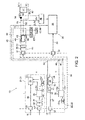
- Fig. 2 it is now supplementary Fig. 2 considered, wherein the secondary circuit part 13 of the control circuit 11 of the 3-phase inverter 1 is shown in more detail in a schematic manner.
- the galvanic isolation between the primary-side circuit part 12 and the secondary-side circuit part 13 is as in Fig. 1 indicated by a dashed dividing line 14.
- the TOP driver circuit 21 for controlling the TOP switches 8 and the BOT driver circuit 22 for controlling the BOT switches 9 are shown in more detail. Accordingly, the TOP driver circuit 21 comprises, for each half bridge 3, a TOP driver subcircuit 31 which serves to drive the TOP switch 8 in the associated half bridge 3. For the purpose of a simpler representation is in Fig. 2 only a single TOP driver subcircuit 31 is shown, it being understood that a separate TOP driver subcircuit 31 is provided for each half bridge 3.
- Each TOP driver subcircuit 31 comprises a push-pull output stage 34 for generating the TOP control voltage 23 as a function of the logic level of the TOP control signal 16 (PWM signal) supplied via an optocoupler 33.
- the TOP control voltage 23 generated by the push-pull output stage 34 is applied directly to the control input of the associated TOP switch 8, the TOP switch 8 being switched on, for example, at a high logic level, whereas the TOP switch 8 is activated at a low logic level is turned off.
- the optocoupler 33 is used for electrical isolation of the primary and secondary circuit part 12, 13 in the region of the TOP driver subcircuit 31.
- Each TOP driver subcircuit 31 further comprises a TOP supply device 35 for supplying the TOP driver subcircuit 31 with a first secondary side operating voltage of, for example, +15 / -8 volts.
- a second secondary-side operating voltage of, for example, +5 volts is generated from the first secondary-side operating voltage.
- the generation of the first secondary-side operating voltage of, for example +15 / -8 volts is coupled to at least one of the primary-side operating voltages, so that in case of failure of a primary-side operating voltage usually fail the secondary side operating voltages.
- the TOP driver supply 35 comprises for this purpose an internal driver power supply 40 with potential separation, which has in a conventional manner via a transformer 37 for power transmission, a rectifier 38 and a filter capacitor 39 for voltage smoothing.
- the switching power supply 40 is clocked by a primary-side operating voltage.
- the structure and function of such a switched-mode power supply 40 are known per se to those skilled in the art, so that they need not be discussed in more detail here.
- the BOT driver circuit 22 for each half-bridge 3 comprises a BOT driver subcircuit 32 which is used to drive the BOT switch 9 in the associated one Half bridge 3 is used.
- a BOT driver subcircuit 32 is shown, it being understood that a separate BOT driver subcircuit 32 is provided for each half bridge 3.
- Each BOT driver subcircuit 32 comprises a push-pull output stage 34 for generating the BOT control voltage 24 on the basis of the BOT control signal 17 (PWM signal) supplied via an optocoupler 33.
- the BOT control voltage 24 generated by the push-pull output stage 34 is applied directly to the control input of the associated BOT switch 9.
- the optocoupler 33 serves for galvanic isolation of the primary and secondary circuit part 12, 13 in the area of the BOT driver subcircuit 32.
- the push-pull output stage 34 is preceded by a logical OR gate 41, to which the BOT control signal 17 is applied as the first input signal.
- the second input signal to the OR gate 41 is a BOT driver signal 42, which will be discussed in more detail below.
- the OR gate 41 generates at its signal output an OR gate signal 53 having a high logic level if a high logic level of the first input signal and / or a high logic level of the second input signal is present, or an OR gate signal 53 of a low logic level if a low logic level of the first input signal or no input signal and / or a low logic level of the second input signal or no second input signal.
- the push-pull output stage 34 is driven via the OR gate signal 53, wherein here, for example, at a high logic level of the OR gate signal 53 of the BOT switch 9 is turned on, whereas at a low logic level of the OR gate signal 53 of the BOT switch 9 is turned off.
- the optocoupler 33 serves for galvanic isolation of the primary and secondary circuit part 12, 13 in the area of the BOT driver subcircuit 32.
- Each BOT driver subcircuit 32 further comprises a BOT supply device 36 for supplying the BOT driver subcircuit 32 with a first secondary side operating voltage of, for example, +15 / -8 volts.
- a second secondary-side operating voltage of, for example, +5 volts is generated from the first secondary-side operating voltage.
- a common supply of the BOT supply devices 36 takes place with the first secondary-side operating voltage by a secondary-side supply device 43 in the secondary-side circuit part 13 of the control circuit 11.
- the secondary-side supply device 43 is coupled to at least one primary side operating voltage.
- the secondary-side supply device 43 comprises a switched-mode power supply 40 with potential separation, which has a transformer 37 for power transmission, a rectifier 38 and a filter capacitor 39 for voltage smoothing.
- the switching power supply 40 is clocked by a primary-side operating voltage, so that in case of failure of at least one primary-side operating voltage usually a failure of the secondary-side operating voltages is the result.
- additional additional supply means 57 which are connected to the secondary-side supply device 43, further secondary-side operating voltages of, for example, 1.5 volts, 3.3 volts and 5 volts are generated from the first secondary-side operating voltage. These serve to feed the additional circuit 25.
- a first electrical supply line 44 and a second electrical supply line 45 are provided for feeding the three BOT driver subcircuits 32 with the first secondary-side operating voltage, wherein the first supply line 44 to a first voltage output 49 and the second supply line 45 to a second voltage output 50 to Provision of the first secondary-side operating voltage (+ 15 / -8 volts) are connected.
- the BOT supply devices 36 each access the potentials on the supply lines 44, 45 via a first voltage tap 46 and a second voltage tap 47.
- the driver subcircuits 31, 32 generally comprise a number of further circuit elements, for example a device for monitoring the collector-emitter voltage or a device for detecting a driver undervoltage, which will not be described in detail here.
- the additional circuit 25 is connected to the intermediate circuit voltage (DC +, DC-) DC / DC converter (DC / DC converter) 27 as a backup power supply in case of failure of the secondary side supply device 43.
- a first voltage output 49 'of the DC / DC converter 27 connected by a first electrical connection line 51 to the first voltage output 49 of the secondary side supply device 43, while a second voltage output 50 'of the DC / DC converter 27 is connected by a second electrical connection line 53 to the secondary side supply device 43, that's his Potential at the second voltage output 50 of the secondary-side supply device 43 is applied.
- the first supply line 44 is connected here, for example, to the first connecting line 51, the second supply line 45 to the second voltage output 50 of the secondary-side supply device 43.
- the DC / DC converter 27 converts the intermediate circuit voltage (DC +, DC-) into a DC voltage suitable for operating the additional circuit 25 and the BOT driver circuit 22 or BOT driver subcircuits 32, respectively.
- the DC / DC converter 27 converts the upper potential (DC +), for example, to a potential of +12 volts, which is applied to the first voltage output 49 ', while the lower potential (DC-) is converted to a potential of 0 volts which is applied to the second voltage output 50 '. If the secondary-side supply device 43 fails, the potentials +12.0 volts of the DC / DC converter 27 are thus applied to the voltage outputs 49, 50 of the secondary-side supply device 43.
- the equivalent voltage (+12.0 volts) generated by the DC / DC converter 27 is provided simultaneously with the first secondary operating voltage (+ 15 / -8 volts), being less than the first secondary operating voltage, so that the first secondary one Operating voltage is intended to supply voltage. In addition, a current flow to the DC / DC converter 27 can thereby be prevented.
- the first voltage output 49 'of the DC / DC converter 27 is connected to the first voltage output 49 of the secondary-side supply device 43 with the interposition of a current valve designed as a diode 54.
- the diode 54 is arranged so that current flow to the DC / DC converter 27 is blocked, but allowed in the opposite direction.
- the DC / DC converter 27 must provide a sufficient charge current, which can always be ensured.
- the additional circuit 25 has the control logic module 26 which, with the interposition of an opto-coupler 33, the error signal 28 generated by the comparator 29 received as input signal.
- the control logic module 26 is set up in such a way that, on the basis of the error signal 28, it generates the already mentioned BOT driver signal 42, which is impressed via a signal output of a BOT driver signal line 55, which is not specifically described.
- the BOT driver subcircuit 32 the BOT drive signal 42 is tapped from the BOT drive signal line 55 via a signal tap 56 and applied to the OR gate 41 as a second input signal.
- a BOT drive signal 42 is generated at a high logic level (High)
- a BOT drive signal 42 is at a low logic level (Low) is generated if an error signal 28 with a high logic level (High) is applied, which indicates the error-free operation of the primary-side circuit part 12.
- the control logic module 26 is supplied in normal operation of the secondary side supply device 43 and the auxiliary supply means 57 with its operating voltages, which in Fig. 2 not shown in detail.
- the voltage outputs 49, 50 of the secondary-side supply device 43 are acted upon by the equivalent voltage generated by the DC / DC converter 27, so that (in addition to further logic components of the additional circuit 25) a substitute power supply of the control logic module 26 takes place.
- the control logic module 26 is supplied via an analog-to-digital converter (A / D converter) 48, the DC voltage generated by the DC / DC converter 27 as an input signal.
- a / D converter 48 An unspecified signal input of the A / D converter 48 is connected to the first connection line 51 for this purpose.
- the A / D converter 48 is fed in normal operation by the secondary-side supply device 43 (and possibly the additional supply devices 57). In the event of a failure of the secondary-side supply device 43, the DC / DC converter 27 assumes the function of the secondary-side supply device 43.
- the comparator 29 In the error-free case, in which the primary-side operating voltages are error-free, the comparator 29 generates an error signal 28 with an example low logic level, so that generated on the basis of a drive signal 19 TOP and BOT control signals 16, 17 unhindered to the TOP or BOT driver circuit 21, 22 for generating the TOP or BOT control voltages 23, 24 are forwarded. Accordingly, the first secondary-side operating voltage (+ 15 / -8 volts) from the secondary-side supply device 43 as well as all other secondary-side operating voltage is provided by the auxiliary supply devices 57. At the same time, the DC / DC converter 27 converts the intermediate circuit voltage (DC +, DC-) into a substitute voltage (+12/0 volts).
- the comparator 29 In the event of a fault, in which at least one primary-side operating voltage fails, the comparator 29 generates an error signal 28 having, for example, a high logic level, so that the TOP and BOT control signals 16, 17 generated on the basis of a drive signal 19 in the safety logic module 20 are blocked due to the error signal 28 and not forwarded to the TOP and BOT driver circuits 21, 22, respectively.
- the secondary-side supply device 43 does not generate a secondary-side operating voltage in this case, so that the two potential outputs voltage outputs 49, 50 of the secondary-side supply device 43 are acted upon by the equivalent voltage converted by the DC link converter 27 from the intermediate circuit voltage (DC +, DC-) ,
- the BOT supply means 36 and the additional circuit 25 are fed by the equivalent voltage of the DC / DC converter 27.
- the control logic chip 26, due to the high logic level of the error signal 28, generates a BOT drive signal 42 having, for example, a high logic level, such that an OR gate signal 53 for turning on the BOT drive sub-circuit 32 through the BOT drive signal 42 present at the OR gate 41 BOT switch 9 is generated.
- control logic block 26 circuit and / or program technology is set up so that with appropriate control by the error signal 28 switching on all BOT switch 9 by the BOT driver signal 42 only with a certain time delay of for example a few microseconds after switching off the TOP switch 8 is done to avoid a short circuit of the voltage intermediate circuit 6.
- the control logic module 25 is furthermore set up in terms of circuitry and / or programming such that all BOT switches 9 are only switched on when the DC / DC converter 27 provides an equivalent voltage of a predetermined or predefinable magnitude (for example +12 volts).
- the control logic block 25 is transmitted for this purpose via the A / D converter 48, a digital voltage value as an input signal. If the DC / DC converter 27 does not provide sufficient backup voltage, the BOT switch 9 is not turned on by the BOT drive signal 42.
- control circuit module 25 the DC link voltage (DC +, DC-) is transmitted as an input signal, which in Fig. 2 not shown in detail.
- the control logic block 25 circuit and / or program is set up so that a short-circuiting of the BOT switch 9 by the BOT driver signal 42 only takes place when the DC link voltage exceeds a predetermined or predetermined upper voltage threshold (eg 420 volts) and a predetermined or predefinable lower voltage threshold (eg 60 volts) does not fall below.
- a predetermined or predetermined upper voltage threshold eg 420 volts
- a predetermined or predefinable lower voltage threshold eg 60 volts
- the BOT switch 9 is turned on by the BOT drive signal 42 only when the DC link voltage is equal to or less than the upper voltage threshold.
- the short circuit of the load outputs 10 triggered by the BOT drive signal 42 is canceled by switching off all BOT switches 9 when the intermediate circuit voltage falls below the lower voltage threshold.
- the inventive 3-phase inverter 1 thus creates for the first time the possibility that in case of failure or deviation from the setpoint of a primary-side operating voltage, which usually also has a failure of the secondary-side operating voltages result, all BOT switches 9 are reliably and safely turned on to short-circuit the load outputs 10 of the half bridges 3. This is achieved by an alternative voltage supply of the logic components of the BOT driver circuit 22 and the additional circuit 25 by the DC / DC converter 27, which generates a replacement voltage of suitable size from the intermediate circuit voltage.
- a control of the BOT switch 9 in the event of an error occurs by a common BOT driver signal 42 which is generated by the control logic module 26 on the basis of the error signal 28.
- the power converter according to the invention is characterized by a technically simple, cost-effective and at the same time robust construction.
- the equivalent voltage generated by the DC / DC converter 27 is immediately applied to the components to be supplied, which would not be the case if the primary-side circuit part 12 were replaced by a generated from the intermediate circuit voltage operating voltage, as with a considerable time delay
- the replacement voltage supply is to be expected by the galvanic isolation.
- in this case for example, in the case of failure of a logic component of the primary-side circuit part 12 could not be ensured that all BOT switches are turned on at the same time.
Landscapes
- Engineering & Computer Science (AREA)
- Power Engineering (AREA)
- Inverter Devices (AREA)
- Dc-Dc Converters (AREA)
Applications Claiming Priority (1)
| Application Number | Priority Date | Filing Date | Title |
|---|---|---|---|
| DE102012102878A DE102012102878A1 (de) | 2012-04-03 | 2012-04-03 | Stromrichter mit Zwischenkreis, sowie Verfahren zum Betreiben eines solchen Stromrichters |
Publications (3)
| Publication Number | Publication Date |
|---|---|
| EP2648328A2 true EP2648328A2 (fr) | 2013-10-09 |
| EP2648328A3 EP2648328A3 (fr) | 2017-03-22 |
| EP2648328B1 EP2648328B1 (fr) | 2018-05-09 |
Family
ID=47681770
Family Applications (1)
| Application Number | Title | Priority Date | Filing Date |
|---|---|---|---|
| EP13154366.2A Active EP2648328B1 (fr) | 2012-04-03 | 2013-02-07 | Protection d'un convertisseur de courant avec circuit intermédiaire contre les dommages causés par la contre-tension d'une machine synchrone |
Country Status (2)
| Country | Link |
|---|---|
| EP (1) | EP2648328B1 (fr) |
| DE (1) | DE102012102878A1 (fr) |
Cited By (1)
| Publication number | Priority date | Publication date | Assignee | Title |
|---|---|---|---|---|
| CN111758304A (zh) * | 2018-01-26 | 2020-10-09 | 劳斯莱斯德国有限两合公司 | 变流器的模块化的组件和具有这种组件的飞行器 |
Families Citing this family (2)
| Publication number | Priority date | Publication date | Assignee | Title |
|---|---|---|---|---|
| DE102016207195A1 (de) * | 2016-04-27 | 2017-11-02 | Zf Friedrichshafen Ag | System zum aktiven Kurzschließen von Phasen eines Wechselrichters und Kraftfahrzeugantrieb |
| DE102018202662A1 (de) * | 2018-02-22 | 2019-08-22 | Zf Friedrichshafen Ag | Einstellen eines bestimmten Betriebszustands einer elektrischen Maschine eines Fahrzeugs |
Citations (1)
| Publication number | Priority date | Publication date | Assignee | Title |
|---|---|---|---|---|
| DE10251977A1 (de) | 2002-11-08 | 2004-06-03 | Arnold Müller GmbH & Co. KG | Synchronmotor |
Family Cites Families (3)
| Publication number | Priority date | Publication date | Assignee | Title |
|---|---|---|---|---|
| ES2158782B1 (es) * | 1998-05-12 | 2002-03-01 | Mannesmann Sachs Ag | Sistema y procedimiento de mando para un motor electrico excitado permanentemente con al menos una fase. |
| US7554276B2 (en) * | 2005-09-21 | 2009-06-30 | International Rectifier Corporation | Protection circuit for permanent magnet synchronous motor in field weakening operation |
| US7652858B2 (en) * | 2007-06-06 | 2010-01-26 | Gm Global Technology Operations, Inc. | Protection for permanent magnet motor control circuits |
-
2012
- 2012-04-03 DE DE102012102878A patent/DE102012102878A1/de not_active Withdrawn
-
2013
- 2013-02-07 EP EP13154366.2A patent/EP2648328B1/fr active Active
Patent Citations (1)
| Publication number | Priority date | Publication date | Assignee | Title |
|---|---|---|---|---|
| DE10251977A1 (de) | 2002-11-08 | 2004-06-03 | Arnold Müller GmbH & Co. KG | Synchronmotor |
Cited By (2)
| Publication number | Priority date | Publication date | Assignee | Title |
|---|---|---|---|---|
| CN111758304A (zh) * | 2018-01-26 | 2020-10-09 | 劳斯莱斯德国有限两合公司 | 变流器的模块化的组件和具有这种组件的飞行器 |
| CN111758304B (zh) * | 2018-01-26 | 2022-05-17 | 劳斯莱斯德国有限两合公司 | 变流器的模块化的组件和具有这种组件的飞行器 |
Also Published As
| Publication number | Publication date |
|---|---|
| DE102012102878A1 (de) | 2013-10-10 |
| EP2648328B1 (fr) | 2018-05-09 |
| EP2648328A3 (fr) | 2017-03-22 |
Similar Documents
| Publication | Publication Date | Title |
|---|---|---|
| EP2893604B1 (fr) | Circuit d'état de fonctionnement d'un onduleur et procédé de réglage des états de fonctionnement d'un onduleur | |
| EP2639916A2 (fr) | Circuit pour convertisseur de courant avec circuit intermédiaire, ainsi que procédé de fonctionnement d'un convertisseur de courant | |
| DE102012101508A1 (de) | Verfahren und Vorrichtung zum Betreiben einer elektrischen Maschine | |
| EP2764594A1 (fr) | Dispositif et procédé pour décharger un condensateur d'un onduleur | |
| WO2014060181A1 (fr) | Agencement de circuit de protection pour un réseau multitension | |
| DE102015206627A1 (de) | Selbstsichernder Umrichter | |
| WO2017186419A1 (fr) | Dispositif onduleur, système d'entraînement électrique et procédé de décharge d'un condensateur de circuit intermédiaire dans un dispositif onduleur | |
| EP2794334A1 (fr) | Dispositif de commande pour commutateur à semi-conducteur d'un onduleur et procédé permettant de commander un onduleur | |
| DE102013225603B4 (de) | Stromrichtervorrichtung für eine Ein- oder Mehrachsanordnung und Betriebsverfahren | |
| DE102015013875B4 (de) | Wechselrichter für eine elektrische Maschine, elektrische Antriebseinrichtung für ein Kraftfahrzeug sowie Verfahren zum Betreiben eines Wechselrichters | |
| EP2648328B1 (fr) | Protection d'un convertisseur de courant avec circuit intermédiaire contre les dommages causés par la contre-tension d'une machine synchrone | |
| EP2570291A1 (fr) | Système d'entraînement d'un véhicule fonctionnant sur batterie doté d'une machine synchrone à excitation permanente alimentée par convertisseur | |
| WO2011057900A2 (fr) | Onduleur | |
| EP3600943B1 (fr) | Convertisseur continu-continu, dispositif d'alimentation électrique et procédé de diagnostic pour convertisseur continu-continu | |
| DE102008056400A1 (de) | Umrichterschaltung mit Überspannungsschutz | |
| DE102013224891B4 (de) | Schaltungsanordnung | |
| WO2016012301A1 (fr) | Procédé de commande d'au moins une machine électrique pouvant fonctionner en générateur et moyen pour mettre en œuvre celui-ci | |
| EP2654155B1 (fr) | Convertisseur de courant, tout comme procédé destiné au fonctionnement d'un convertisseur de courant | |
| DE102012109283A1 (de) | Stromrichter mit Zusatzschaltung, sowie Verfahren zum Betreiben eines Stromrichters | |
| EP2670042B1 (fr) | Convertisseur doté d'une mesure de tension de circuit intermédiaire redondante tout comme procédé destiné au fonctionnement d'un convertisseur de courant | |
| EP3061186B1 (fr) | Demi-pont pour redresseur actif | |
| WO2018177770A1 (fr) | Procédé de diagnostic pour onduleur, dispositif onduleur et système d'entraînement électrique | |
| WO2024068076A1 (fr) | Procédé et dispositif pour interrompre un processus de charge d'une source d'alimentation d'un entraînement électrique | |
| DE102022113800A1 (de) | Verfahren zum Betrieb einer elektrischen Maschine, insbesondere in einem Kraftfahrzeug, und Kraftfahrzeug | |
| WO2024033073A1 (fr) | Onduleur avec transistor pour isoler les surintensités entre une batterie et un condensateur de liaison à courant continu |
Legal Events
| Date | Code | Title | Description |
|---|---|---|---|
| PUAI | Public reference made under article 153(3) epc to a published international application that has entered the european phase |
Free format text: ORIGINAL CODE: 0009012 |
|
| AK | Designated contracting states |
Kind code of ref document: A2 Designated state(s): AL AT BE BG CH CY CZ DE DK EE ES FI FR GB GR HR HU IE IS IT LI LT LU LV MC MK MT NL NO PL PT RO RS SE SI SK SM TR |
|
| AX | Request for extension of the european patent |
Extension state: BA ME |
|
| PUAL | Search report despatched |
Free format text: ORIGINAL CODE: 0009013 |
|
| AK | Designated contracting states |
Kind code of ref document: A3 Designated state(s): AL AT BE BG CH CY CZ DE DK EE ES FI FR GB GR HR HU IE IS IT LI LT LU LV MC MK MT NL NO PL PT RO RS SE SI SK SM TR |
|
| AX | Request for extension of the european patent |
Extension state: BA ME |
|
| RIC1 | Information provided on ipc code assigned before grant |
Ipc: H02M 7/48 20070101AFI20170213BHEP Ipc: H02M 1/32 20070101ALI20170213BHEP |
|
| STAA | Information on the status of an ep patent application or granted ep patent |
Free format text: STATUS: REQUEST FOR EXAMINATION WAS MADE |
|
| 17P | Request for examination filed |
Effective date: 20170922 |
|
| RBV | Designated contracting states (corrected) |
Designated state(s): AL AT BE BG CH CY CZ DE DK EE ES FI FR GB GR HR HU IE IS IT LI LT LU LV MC MK MT NL NO PL PT RO RS SE SI SK SM TR |
|
| GRAP | Despatch of communication of intention to grant a patent |
Free format text: ORIGINAL CODE: EPIDOSNIGR1 |
|
| STAA | Information on the status of an ep patent application or granted ep patent |
Free format text: STATUS: GRANT OF PATENT IS INTENDED |
|
| GRAS | Grant fee paid |
Free format text: ORIGINAL CODE: EPIDOSNIGR3 |
|
| INTG | Intention to grant announced |
Effective date: 20180307 |
|
| GRAA | (expected) grant |
Free format text: ORIGINAL CODE: 0009210 |
|
| STAA | Information on the status of an ep patent application or granted ep patent |
Free format text: STATUS: THE PATENT HAS BEEN GRANTED |
|
| AK | Designated contracting states |
Kind code of ref document: B1 Designated state(s): AL AT BE BG CH CY CZ DE DK EE ES FI FR GB GR HR HU IE IS IT LI LT LU LV MC MK MT NL NO PL PT RO RS SE SI SK SM TR |
|
| REG | Reference to a national code |
Ref country code: GB Ref legal event code: FG4D Free format text: NOT ENGLISH |
|
| REG | Reference to a national code |
Ref country code: CH Ref legal event code: EP Ref country code: AT Ref legal event code: REF Ref document number: 998420 Country of ref document: AT Kind code of ref document: T Effective date: 20180515 |
|
| REG | Reference to a national code |
Ref country code: DE Ref legal event code: R096 Ref document number: 502013010096 Country of ref document: DE Ref country code: IE Ref legal event code: FG4D Free format text: LANGUAGE OF EP DOCUMENT: GERMAN |
|
| REG | Reference to a national code |
Ref country code: NL Ref legal event code: MP Effective date: 20180509 |
|
| REG | Reference to a national code |
Ref country code: LT Ref legal event code: MG4D |
|
| PG25 | Lapsed in a contracting state [announced via postgrant information from national office to epo] |
Ref country code: SE Free format text: LAPSE BECAUSE OF FAILURE TO SUBMIT A TRANSLATION OF THE DESCRIPTION OR TO PAY THE FEE WITHIN THE PRESCRIBED TIME-LIMIT Effective date: 20180509 Ref country code: ES Free format text: LAPSE BECAUSE OF FAILURE TO SUBMIT A TRANSLATION OF THE DESCRIPTION OR TO PAY THE FEE WITHIN THE PRESCRIBED TIME-LIMIT Effective date: 20180509 Ref country code: LT Free format text: LAPSE BECAUSE OF FAILURE TO SUBMIT A TRANSLATION OF THE DESCRIPTION OR TO PAY THE FEE WITHIN THE PRESCRIBED TIME-LIMIT Effective date: 20180509 Ref country code: FI Free format text: LAPSE BECAUSE OF FAILURE TO SUBMIT A TRANSLATION OF THE DESCRIPTION OR TO PAY THE FEE WITHIN THE PRESCRIBED TIME-LIMIT Effective date: 20180509 Ref country code: NO Free format text: LAPSE BECAUSE OF FAILURE TO SUBMIT A TRANSLATION OF THE DESCRIPTION OR TO PAY THE FEE WITHIN THE PRESCRIBED TIME-LIMIT Effective date: 20180809 Ref country code: BG Free format text: LAPSE BECAUSE OF FAILURE TO SUBMIT A TRANSLATION OF THE DESCRIPTION OR TO PAY THE FEE WITHIN THE PRESCRIBED TIME-LIMIT Effective date: 20180809 |
|
| PG25 | Lapsed in a contracting state [announced via postgrant information from national office to epo] |
Ref country code: GR Free format text: LAPSE BECAUSE OF FAILURE TO SUBMIT A TRANSLATION OF THE DESCRIPTION OR TO PAY THE FEE WITHIN THE PRESCRIBED TIME-LIMIT Effective date: 20180810 Ref country code: NL Free format text: LAPSE BECAUSE OF FAILURE TO SUBMIT A TRANSLATION OF THE DESCRIPTION OR TO PAY THE FEE WITHIN THE PRESCRIBED TIME-LIMIT Effective date: 20180509 Ref country code: RS Free format text: LAPSE BECAUSE OF FAILURE TO SUBMIT A TRANSLATION OF THE DESCRIPTION OR TO PAY THE FEE WITHIN THE PRESCRIBED TIME-LIMIT Effective date: 20180509 Ref country code: LV Free format text: LAPSE BECAUSE OF FAILURE TO SUBMIT A TRANSLATION OF THE DESCRIPTION OR TO PAY THE FEE WITHIN THE PRESCRIBED TIME-LIMIT Effective date: 20180509 Ref country code: HR Free format text: LAPSE BECAUSE OF FAILURE TO SUBMIT A TRANSLATION OF THE DESCRIPTION OR TO PAY THE FEE WITHIN THE PRESCRIBED TIME-LIMIT Effective date: 20180509 |
|
| PG25 | Lapsed in a contracting state [announced via postgrant information from national office to epo] |
Ref country code: DK Free format text: LAPSE BECAUSE OF FAILURE TO SUBMIT A TRANSLATION OF THE DESCRIPTION OR TO PAY THE FEE WITHIN THE PRESCRIBED TIME-LIMIT Effective date: 20180509 Ref country code: SK Free format text: LAPSE BECAUSE OF FAILURE TO SUBMIT A TRANSLATION OF THE DESCRIPTION OR TO PAY THE FEE WITHIN THE PRESCRIBED TIME-LIMIT Effective date: 20180509 Ref country code: PL Free format text: LAPSE BECAUSE OF FAILURE TO SUBMIT A TRANSLATION OF THE DESCRIPTION OR TO PAY THE FEE WITHIN THE PRESCRIBED TIME-LIMIT Effective date: 20180509 Ref country code: EE Free format text: LAPSE BECAUSE OF FAILURE TO SUBMIT A TRANSLATION OF THE DESCRIPTION OR TO PAY THE FEE WITHIN THE PRESCRIBED TIME-LIMIT Effective date: 20180509 Ref country code: RO Free format text: LAPSE BECAUSE OF FAILURE TO SUBMIT A TRANSLATION OF THE DESCRIPTION OR TO PAY THE FEE WITHIN THE PRESCRIBED TIME-LIMIT Effective date: 20180509 Ref country code: CZ Free format text: LAPSE BECAUSE OF FAILURE TO SUBMIT A TRANSLATION OF THE DESCRIPTION OR TO PAY THE FEE WITHIN THE PRESCRIBED TIME-LIMIT Effective date: 20180509 |
|
| REG | Reference to a national code |
Ref country code: DE Ref legal event code: R097 Ref document number: 502013010096 Country of ref document: DE |
|
| PG25 | Lapsed in a contracting state [announced via postgrant information from national office to epo] |
Ref country code: SM Free format text: LAPSE BECAUSE OF FAILURE TO SUBMIT A TRANSLATION OF THE DESCRIPTION OR TO PAY THE FEE WITHIN THE PRESCRIBED TIME-LIMIT Effective date: 20180509 Ref country code: IT Free format text: LAPSE BECAUSE OF FAILURE TO SUBMIT A TRANSLATION OF THE DESCRIPTION OR TO PAY THE FEE WITHIN THE PRESCRIBED TIME-LIMIT Effective date: 20180509 |
|
| PLBE | No opposition filed within time limit |
Free format text: ORIGINAL CODE: 0009261 |
|
| STAA | Information on the status of an ep patent application or granted ep patent |
Free format text: STATUS: NO OPPOSITION FILED WITHIN TIME LIMIT |
|
| 26N | No opposition filed |
Effective date: 20190212 |
|
| PG25 | Lapsed in a contracting state [announced via postgrant information from national office to epo] |
Ref country code: SI Free format text: LAPSE BECAUSE OF FAILURE TO SUBMIT A TRANSLATION OF THE DESCRIPTION OR TO PAY THE FEE WITHIN THE PRESCRIBED TIME-LIMIT Effective date: 20180509 |
|
| REG | Reference to a national code |
Ref country code: CH Ref legal event code: PL |
|
| GBPC | Gb: european patent ceased through non-payment of renewal fee |
Effective date: 20190207 |
|
| PG25 | Lapsed in a contracting state [announced via postgrant information from national office to epo] |
Ref country code: LU Free format text: LAPSE BECAUSE OF NON-PAYMENT OF DUE FEES Effective date: 20190207 Ref country code: MC Free format text: LAPSE BECAUSE OF FAILURE TO SUBMIT A TRANSLATION OF THE DESCRIPTION OR TO PAY THE FEE WITHIN THE PRESCRIBED TIME-LIMIT Effective date: 20180509 |
|
| REG | Reference to a national code |
Ref country code: BE Ref legal event code: MM Effective date: 20190228 |
|
| REG | Reference to a national code |
Ref country code: IE Ref legal event code: MM4A |
|
| PG25 | Lapsed in a contracting state [announced via postgrant information from national office to epo] |
Ref country code: AL Free format text: LAPSE BECAUSE OF FAILURE TO SUBMIT A TRANSLATION OF THE DESCRIPTION OR TO PAY THE FEE WITHIN THE PRESCRIBED TIME-LIMIT Effective date: 20180509 |
|
| PG25 | Lapsed in a contracting state [announced via postgrant information from national office to epo] |
Ref country code: CH Free format text: LAPSE BECAUSE OF NON-PAYMENT OF DUE FEES Effective date: 20190228 Ref country code: LI Free format text: LAPSE BECAUSE OF NON-PAYMENT OF DUE FEES Effective date: 20190228 |
|
| PG25 | Lapsed in a contracting state [announced via postgrant information from national office to epo] |
Ref country code: GB Free format text: LAPSE BECAUSE OF NON-PAYMENT OF DUE FEES Effective date: 20190207 Ref country code: IE Free format text: LAPSE BECAUSE OF NON-PAYMENT OF DUE FEES Effective date: 20190207 |
|
| PG25 | Lapsed in a contracting state [announced via postgrant information from national office to epo] |
Ref country code: FR Free format text: LAPSE BECAUSE OF NON-PAYMENT OF DUE FEES Effective date: 20190228 Ref country code: BE Free format text: LAPSE BECAUSE OF NON-PAYMENT OF DUE FEES Effective date: 20190228 |
|
| PG25 | Lapsed in a contracting state [announced via postgrant information from national office to epo] |
Ref country code: TR Free format text: LAPSE BECAUSE OF FAILURE TO SUBMIT A TRANSLATION OF THE DESCRIPTION OR TO PAY THE FEE WITHIN THE PRESCRIBED TIME-LIMIT Effective date: 20180509 |
|
| REG | Reference to a national code |
Ref country code: AT Ref legal event code: MM01 Ref document number: 998420 Country of ref document: AT Kind code of ref document: T Effective date: 20190207 |
|
| PG25 | Lapsed in a contracting state [announced via postgrant information from national office to epo] |
Ref country code: AT Free format text: LAPSE BECAUSE OF NON-PAYMENT OF DUE FEES Effective date: 20190207 |
|
| PG25 | Lapsed in a contracting state [announced via postgrant information from national office to epo] |
Ref country code: MT Free format text: LAPSE BECAUSE OF FAILURE TO SUBMIT A TRANSLATION OF THE DESCRIPTION OR TO PAY THE FEE WITHIN THE PRESCRIBED TIME-LIMIT Effective date: 20180509 Ref country code: PT Free format text: LAPSE BECAUSE OF FAILURE TO SUBMIT A TRANSLATION OF THE DESCRIPTION OR TO PAY THE FEE WITHIN THE PRESCRIBED TIME-LIMIT Effective date: 20180910 |
|
| PG25 | Lapsed in a contracting state [announced via postgrant information from national office to epo] |
Ref country code: CY Free format text: LAPSE BECAUSE OF FAILURE TO SUBMIT A TRANSLATION OF THE DESCRIPTION OR TO PAY THE FEE WITHIN THE PRESCRIBED TIME-LIMIT Effective date: 20180509 |
|
| PG25 | Lapsed in a contracting state [announced via postgrant information from national office to epo] |
Ref country code: IS Free format text: LAPSE BECAUSE OF FAILURE TO SUBMIT A TRANSLATION OF THE DESCRIPTION OR TO PAY THE FEE WITHIN THE PRESCRIBED TIME-LIMIT Effective date: 20180909 |
|
| PG25 | Lapsed in a contracting state [announced via postgrant information from national office to epo] |
Ref country code: HU Free format text: LAPSE BECAUSE OF FAILURE TO SUBMIT A TRANSLATION OF THE DESCRIPTION OR TO PAY THE FEE WITHIN THE PRESCRIBED TIME-LIMIT; INVALID AB INITIO Effective date: 20130207 |
|
| PG25 | Lapsed in a contracting state [announced via postgrant information from national office to epo] |
Ref country code: MK Free format text: LAPSE BECAUSE OF FAILURE TO SUBMIT A TRANSLATION OF THE DESCRIPTION OR TO PAY THE FEE WITHIN THE PRESCRIBED TIME-LIMIT Effective date: 20180509 |
|
| PGFP | Annual fee paid to national office [announced via postgrant information from national office to epo] |
Ref country code: DE Payment date: 20240229 Year of fee payment: 12 |