EP2647727A1 - Bacterial conductive fibres - Google Patents
Bacterial conductive fibres Download PDFInfo
- Publication number
- EP2647727A1 EP2647727A1 EP13162128.6A EP13162128A EP2647727A1 EP 2647727 A1 EP2647727 A1 EP 2647727A1 EP 13162128 A EP13162128 A EP 13162128A EP 2647727 A1 EP2647727 A1 EP 2647727A1
- Authority
- EP
- European Patent Office
- Prior art keywords
- conductive
- cells
- chain
- subfibre
- fibres
- Prior art date
- Legal status (The legal status is an assumption and is not a legal conclusion. Google has not performed a legal analysis and makes no representation as to the accuracy of the status listed.)
- Granted
Links
Images




Classifications
-
- C—CHEMISTRY; METALLURGY
- C12—BIOCHEMISTRY; BEER; SPIRITS; WINE; VINEGAR; MICROBIOLOGY; ENZYMOLOGY; MUTATION OR GENETIC ENGINEERING
- C12N—MICROORGANISMS OR ENZYMES; COMPOSITIONS THEREOF; PROPAGATING, PRESERVING, OR MAINTAINING MICROORGANISMS; MUTATION OR GENETIC ENGINEERING; CULTURE MEDIA
- C12N1/00—Microorganisms; Compositions thereof; Processes of propagating, maintaining or preserving microorganisms or compositions thereof; Processes of preparing or isolating a composition containing a microorganism; Culture media therefor
- C12N1/20—Bacteria; Culture media therefor
-
- C—CHEMISTRY; METALLURGY
- C12—BIOCHEMISTRY; BEER; SPIRITS; WINE; VINEGAR; MICROBIOLOGY; ENZYMOLOGY; MUTATION OR GENETIC ENGINEERING
- C12N—MICROORGANISMS OR ENZYMES; COMPOSITIONS THEREOF; PROPAGATING, PRESERVING, OR MAINTAINING MICROORGANISMS; MUTATION OR GENETIC ENGINEERING; CULTURE MEDIA
- C12N13/00—Treatment of microorganisms or enzymes with electrical or wave energy, e.g. magnetism, sonic waves
-
- B—PERFORMING OPERATIONS; TRANSPORTING
- B82—NANOTECHNOLOGY
- B82Y—SPECIFIC USES OR APPLICATIONS OF NANOSTRUCTURES; MEASUREMENT OR ANALYSIS OF NANOSTRUCTURES; MANUFACTURE OR TREATMENT OF NANOSTRUCTURES
- B82Y5/00—Nanobiotechnology or nanomedicine, e.g. protein engineering or drug delivery
Definitions
- the present invention relates to a conductive electronic material based on conductive fibres from bacterial cells, which comprise a plurality of such conductive fibres and subfibre filaments arranged in parallel in the periphery of a chain of cells.
- nanoscale materials such as nanowires
- electrical conduits between nanocomponents is associated with significant problems in nanoelectronics.
- Suitable materials must provide sufficient conductivity, and low production costs.
- protein structures such as amyloid fibrils
- Metallization has been considered, but under industrial conditions can be deleterious to protein structure and integrity.
- pilins small protein subunits
- pilus or pili extracellular structured fibers
- Geobacteraceae members of the family Geobacteraceae, for instance, produce pili to facilitate electron transfer to external, solid electron acceptors.
- Some microorganisms such as Shewanella and Geothrix species, may transfer electrons from the cell to the iron oxide surface via excretion of soluble electron-shuttling compounds whereas others, such as Geobacter species, require direct contact with the oxide surface.
- Geobacter metallireducens specifically produced pili during growth on Fe(III) oxide, but not during growth on soluble, chelated Fe(III). Childers, S. E., Ciufo, S. & Lovley, D. R. Geobacter metallireducens accesses insoluble Fe(III) oxide by chemotaxis. Nature 416, 767-769 (2002 ).
- the present invention provides microbial cellular wires and related electronic components and device structures, systems and methods for production and/or assembly, which overcome various deficiencies and shortcomings in the nanoelectronic art.
- the cellular wires are conductive fibres and/or subfibre filaments, which have been identified within a chain of bacterial cells.
- the present invention relates to a conductive electronic material comprising or consisting of one or more conductive fibres and/or subfibre filaments of a chain of bacterial cells, which comprise a plurality of said conductive fibres and/or subfibre filaments arranged in parallel in the periplasmic space along the length and around the periphery of said chain of cells, wherein the outside of said chain of cells is non-conductive.
- the invention relates to a method of preparing a conductive electronic material consisting of conductive fibres and/or subfibre filaments, said method comprising
- the invention also in one aspect relates to a use of a chain of bacterial cells comprising a plurality of parallel conductive fibres and/or subfibre filaments located in the periplasmic space along the length and around the periphery of said chain of cells, wherein the outside of said chain of cells is non-conductive, as a conductive material.
- the invention in one aspect provides an electronic device comprising
- the present invention relates to a chain of cells comprising a plurality of parallel conductive fibres and/or subfibre filaments located in the periplasmic space along the length and around the periphery of said chain of cells, wherein the outside of said chain of cells is non-conductive.
- the invention provides a cell, such as a bacterial cell, which upon proliferation forms a chain of cells comprising a plurality of parallel conductive fibres and/or subfibre filaments located in the periplasmic space along the length and around the periphery of said chain of cells, wherein the outside of said chain of cells is non-conductive.
- the bacterial cell or cells of the invention, or the bacterial cells employed in the invention is preferably a Proteobacteria, such as a Deltaproteobacteria, such as a Desulfobacterales, for example a bacteria belonging to the Desulfobulbus genus.
- a Proteobacteria such as a Deltaproteobacteria, such as a Desulfobacterales, for example a bacteria belonging to the Desulfobulbus genus.
- the present invention provides electronic conductive materials comprising or consisting of microbial cellular wires and related electronic components and device structures, systems and methods for production and/or assembly.
- the invention provides protein-based, naturally conductive cellular wires, which can be used as conductive material without resort to metallization techniques or procedures.
- the present inventors have found that certain bacteria express a plurality of conductive fibres and subfibre filaments. These cells form chains of cells upon growth, and within such a chain of cells, the conductive fibres and subfibre filaments are arranged in parallel in the periplasmic space along the length and around the periphery of said chain of cells.
- the periplasmic space is the space between the cytoplasmic membrane and the outer membrane, which is seen in all gram-negative bacteria.
- each cell of the cell chain has its own cytoplasmic membrane, while the outer membrane is shared by all cells in a filament, thus allowing the fibres to be isolated from the surroundings.
- the fibres within the cells are conductive, while the outside of the chain of cells is non-conductive. Also, each individual fibre within the cell is conductive inside, but non-conductive on the outside; i.e. the fibres are electrically insulated from other/neighbouring fibres within the cells by invaginations of the outer cell membrane.
- the cells have been isolated from marine sediment, and it appears that the fact that the cells form long chains of cells allow the cell colony to support electron transfer using the conductive fibres within the cells over longer distances of several centimetres (e.g. 1-15 cm), such as from within an oxygen-deprived marine sediment to the the sediment-water interface. Thus, the fibres are involved in electron transfer reactions across large numbers of cells over relatively long distances of several centimetres. These biologically produced proteinaceous cellular wires could be useful in micro or nanoelectronic applications.
- the invention provides conductive protein-based, nano- or micro-dimensioned wires or conductive components, produced and self-assembled in vitro or in vivo using a native host or engineered microorganisms.
- conductive fibres and “cellular wires” are used interchangeably herein.
- the chain of bacteria describes above comprises conductive fibres and subfibre filaments, which can be used as wires, e.g. in electronic devices, and such wires are referred to as cellular wires.
- the invention further provides one or more systems or methods for the production and self-assembly of protein-based cellular wires, conductive materials, by the use of microorganisms which can be, optionally, genetically modified to express one or a plurality of conductive fibres and/or subfibre filaments arranged in parallel in the periplasmic space along the length and around the periphery of a chain of cells, wherein the outside of said chain of cells is non-conductive.
- the invention also provides an electronic device structure and/or a circuit or electrical component thereof comprising at least one conductive fibre, subfibre filament or conductive material of the sort described herein, produced and/or self-assembled in vitro or in vivo using the native host or engineered microorganisms.
- the present invention relates to conductive fibres, and use thereof in various micro or nanotechnological applications. More specifically, without limitation, the present invention also provides for the culture of bacteria producing a plurality of conductive fibres and/or subfibre filaments arranged in parallel in the periplasmic space along the length and around the periphery of said chain of cells, wherein the outside of said chain of cells is non-conductive. The invention also provides for isolation of such fibres and/or subfibre filaments and, as well as the fabrication of nano-dimensioned electronic circuit components.
- this invention is directed to a method of preparing a conductive electronic circuit component.
- a method can comprise providing a bacterium capable of expressing a conductive proteinaceous fibres and/or subfibre filaments; providing a culture medium conditioned for conductive fibre production, such a medium comprising an electron acceptor; incubating the bacterium and the medium over a time sufficient for fibre and/or subfibre assembly; and isolating conductive fibres and/or subfibre filaments from the medium.
- conductive fibres and/or subfibre filaments are obtainable from bacterial cells of the present invention.
- the gene or genes encoding the conductive proteinaceous fibres and/or subfibre filaments can be isolated and inserted into plasmids or the genome of a recombinant host cell, which cell is then capable of expressing one or more conductive proteinaceous fibres.
- a recombinant microorganism comprising nucleic acid molecules encoding conductive proteinaceous fibres and/or subfibre filaments of the present invention may also be used in the production of a recombinant material of the present invention.
- the conductive fibres and/or subfibre filaments can be produced and/or obtained from systems comprising one of various strains of the aforementioned fibre-producing species, under appropriate culture conditions, with one or more suitable electron donor components and one or more suitable electron acceptor components, examples of the latter including but not limited to oxygen.
- Electron acceptors could be any compound, but preferably, the electron acceptor is a soluble/dissolved electron acceptor, such as oxygen and/or nitrate. In one embodiment, it is provided that the electron acceptor is not a solid electron acceptor. A preferred electron acceptor is oxygen.
- fibres and/or subfibre filaments can be isolated or extracted from the cells, using various techniques known in the art, and used as described elsewhere herein.
- Conductive fibres and/or subfibre filaments can also be produced and isolated in their soluble form using the native host or engineered microorganisms and assembled as conductive materials into for example electronic components and/or devices in vitro.
- the invention also provides a method of using a cell, preferably a bacterial cell, to prepare an electronic circuit component or electronic device, where that cell express one or more conductive fibres and/or subfibre filaments, which are conductive on the inside and non-conductive on the outside, and when a plurality of fibres and/or subfibre filaments are expressed, the fibres and/or subfibre filaments are arranged in parallel in the periplasmic space along the length and around the periphery of the cell or a chain of cells, wherein the outside of said chain of cells is non-conductive.
- a cell preferably a bacterial cell
- Such a method can comprise providing at least one Proteobacteria, such as a Deltaproteobacteria, such as a Desulfobacterales, for example a bacteria belonging to the Desulfobulbus genus expressing one or more conductive fibres and/or subfibre filaments, which are conductive on the inside and non-conductive on the outside, and when a plurality of fibres are expressed, the fibres and/or subfibre filaments are arranged in parallel in the periplasmic space along the length and around the periphery of the cell or a chain of cells, wherein the outside of said chain of cells is non-conductive; providing a culture medium conditioned for conductive fibre and/or subfibre filament production, such a medium comprising an electron acceptor; and incubating the bacterium or bacteria in the medium over a time sufficient for fibre formation and/or subfibre filament formation.
- Proteobacteria such as a Deltaproteobacteria, such as a Desulfo
- such proteinaceous conductive materials can be expressed by various members of the Desulfobulbus genus and/or Desulfobulbaceae family, or by suitable recombinant hosts.
- one or more conductive fibres can be isolated from the medium. If so, such a method can also comprise in vitro circuit assembly. Manifestation of certain embodiments can comprise application of a voltage across one or more fibre and/or subfibre filaments components.
- the invention is also directed to micro and nano-dimensioned electronic device structures, any of which can comprise a conductive circuit component comprising one or more conductive microbial fibres and/or subfibre filaments.
- a conductive circuit component comprising one or more conductive microbial fibres and/or subfibre filaments.
- a voltage source alone or together with one or more suitably-dimensioned circuit components, as would be known in the art, can be connected with or coupled to one or more conductive fibres and/or subfibre filaments in the fabrication of a particular device structure.
- a main aspect of the present invention relates to a microorganism, in particular a bacterial cell, which comprises genetic material encoding parallel conductive fibres and/or subfibre filaments located in the periplasmic space along the length and around the periphery of the bacteria.
- the conductive fibres and/or subfibre filaments are located around the periphery, and run in parallel along the length of the chain of cells, cf. drawings.
- the bacterial cell is able to form a chain of cells upon growth, where the parallel conductive fibres and/or subfibre filaments are located in the periplasmic space along the length and around the periphery of the chain of cells.
- the invention therefore relates to a bacterial cell, which upon proliferation forms a chain of bacterial cells, said chain comprising a plurality of parallel conductive fibres and/or subfibre filaments located in the periplasmic space along the length and around the periphery of said chain of cells.
- the invention also in one aspect relates to a chain of bacterial cells of the invention as defined herein.
- the invention provides a chain of bacterial cells comprising a plurality of parallel conductive fibres and/or subfibre filaments located in the periplasmic space along the length and around the periphery of said chain of cells, wherein the outside of said chain of cells is non-conductive.
- the conductive fibres and/or subfibre filaments produced by bacterial cells or chain of cells of this invention may be used as conductive fibres and/or subfibre filaments within the cells or they can be extracted from the cells, and used in isolated (non-cellular) form.
- the outside of the bacterial cell or chain of cells is non-conductive, while the fibres and/or subfibre filaments located inside the cells are conductive.
- the conductive fibres and/or subfibre filaments are electrically insulated from the cell surroundings, for example the media or any material used to assemble an electronic device, which incorporate the conductive fibre and/or subfibre material of the invention.
- each individual conductive fibre and/or subfibre filament located within a cell or chain of cells of the invention preferably comprises an insulating layer, which insulates each conductive fibre from neighbouring parallel conductive fibres. This means that each conductive fibre in the bacterial cell can be used to conduct an individual current, which is separate and different from the currents conducted by parallel fibres of the same chain of cells.
- the bacterial cell or in particular, the chain of bacterial cells of the invention comprises a plurality of individual conductive fibres, such as in the order of 2-40, such as 10-30, such as 15-30, for example 20-25 parallel conductive fibres located in the periplasmic space along the length and around the periphery of said one or more cells or chain of cells.
- bacterial cell or in particular, the chain of bacterial cells comprises 24 such parallel conductive fibres.
- each conductive fibre is within the nanometer scale.
- the diameter of a fibre is 10-200 nm, such as 20-190, for example 30-180, such as 40-170, for example 50-160, such as 60-150, for example 70-140, such as 70-130, for example 80-120 nm, such as 85-115, for example 90-110 nm.
- the diameter is around 80-120 nm.
- the length of each conductive fibre depends on the length of the chain of bacterial cell.
- the length of the chain of cells depends on the growth conditions for the cells, and the time allowed for growth.
- the length of the fibres can be manipulated in order to generate fibres of specific sizes depending on the intended use of the fibres.
- the chain of bacterial cells can be from ⁇ m to cm scale, for example from 1 ⁇ m to 10 cm or more.
- the length of a conductive fibre of the invention may range from about 3 ⁇ m (corresponding to one cell) to 10 cm or more, which corresponds to several ten thousands of cells.
- the conductive fibres are 0.001-10 cm in length, for example 0.01-10 cm, such as 0.05-10 cm, for example 0.1-10 cm, such as 0.2-10, such as 0.3-10, such as 0.4-10, such as 0.5-10, such as 0.6-10, such as 0.7-10, such as 0.8-10, such as 0.9-10, for example 1-10 cm, or 2-9 cm, or 3-9, or 3-8 cm in length.
- a chain of bacterial cell of the present invention comprise preferably at least 10 bacterial cells, and may comprise up to several thousand cells, such up to 10,000, for example up to 20,000; 30,000; 40,000; 50,000; 60,000; 70,000; 80,000; 90,000; or 100,000 cells or more.
- a chain of cells comprise of 100-200,000 bacterial cells, such as 10-150,000, or 10-100,000 or 10-50,000 cells, such as 20-1000, for example 30-900 cells, such as 40-800, such as 50-700, such as 60-800, such as 70-700, such as 80-700, such as 90-700, such as 100-700, such as 200-700, such as 300-700, such as 400-800, such as 400-700 cells.
- the bacterial cell is in one embodiment a Proteobacteria, such as a Deltaproteobacteria, such as a Desulfobacterales, for example a bacteria belonging to the Desulfobulbus genus.
- a Proteobacteria such as a Deltaproteobacteria, such as a Desulfobacterales
- the bacterial cell is selected from Proteobacteria.
- the bacterial cell is selected from Deltaproteobacteria.
- the bacterial cell is selected from Desulfobacterales.
- the bacterial cell is selected from Desulfobulbus genus.
- the bacterial cell is selected from the group consisting of Desulfobulbus elongates, Desulfobulbus japonicas, Desulfobulbus mediterraneus, Desulfobulbus propionicus and Desulfobulbus rhabdoformis. In another specific embodiment, the bacterial cell is selected from the group consisting of Desulfobulbus japonicas, Desulfobulbus mediterraneus and Desulfobulbus rhabdoformis.
- the bacterial cell is Desulfobulbus elongates, Desulfobulbus japonicas, Desulfobulbus mediterraneus, Desulfobulbus propionicus or Desulfobulbus rhabdoformis.
- the chain if cells may comprise a mixture of the bacterial cells mentioned herein above.
- a main object of the present invention is to provide a conductive electronic material of the bacteria of the present invention, in particular a chain of such bacteria as explained herein above.
- a main aspect of the invention is therefore a conductive material of bacteria, which produce conductive fibres and/or subfibre filaments, which are arranged in parallel inside the cell in the periphery of the cell membrane.
- the conductive electronic material comprises or consists of one or more conductive fibres of the chain of bacterial cells.
- the conductive fibres and/or subfibre filaments can be used as conductive fibres within the cells, or they can be extracted from the cells, and used in isolated (non-cellular) form.
- the bacterial cells are characterized in that they comprise a plurality of conductive fibres and/or subfibre filaments, which are arranged in parallel in the periplasmic space along the length and around the periphery of the cells.
- the conductive fibres and/or subfibre filaments are located around the periphery, and run in parallel along the length of the chain of cells, cf. drawings.
- the outside of the cells is non-conductive, while the fibres and/or subfibre filaments located inside the cells are conductive, i.e. the conductive fibres and subfibre filaments are insulated by the cell.
- the conductive electronic material of the invention is non-conductive on the outside of the cells.
- each individual conductive fibre preferably comprises an electrically insulating layer, which insulates each conductive fibre from neighbouring parallel conductive fibres.
- each conductive fibre and/or subfibre filaments of the conductive material of the present invention is also conductive on the inside, but non-conductive on the outside. This means that each conductive fibre in the bacterial cell can be used to conduct an individual current, which is separate and different from currents conducted by parallel fibres of the same chain of cells.
- the conductive electronic material comprises or consists of a plurality of individual conductive fibres, such as in the order of 2-40, such as 10-30, such as 15-30, for example 20-25 parallel conductive fibres located in the periplasmic space along the length and around the periphery of the chain of cells.
- the conductive electronic material comprises or consists of 10, 11, 12, 13, 14, 15, 16, 17, 18, 19, 20, 21, 22, 23, 24, 25, 26, 27, 28, 29 or 30 such parallel conductive fibres.
- the conductive electronic material comprises or consists of 17 such parallel conductive fibres.
- the conductive electronic material is a conductive fibre, and in another embodiment, the conductive electronic material is a plurality of conductive fibres.
- each conductive fibre and/or subfibre filaments are described herein above, and may range from 10-200 nm, such as around 80-120 nm in diameter, and 0.0001-10 cm in length.
- the length of the conductive fibres and/or subfibre filaments, which are comprised in the conductive electronic material of the invention, matches the ranges of the lengths of the bacterial chains or fibres.
- a specific conductive material where two or more conductive materials of the present invention are assembled may be even longer.
- Such assemblies comprising multiple conductive materials are also within the scope of the present invention.
- the present invention provides a conductive electronic material comprising or consisting of one or more conductive fibres of a chain of bacterial cells, which comprise a plurality of said conductive fibres and/or subfibre filaments arranged in parallel in the periplasmic space along the length and around the periphery of said chain of cells, wherein the outside of said chain of cells is non-conductive.
- the bacterial cells are Proteobacteria, such as a Deltaproteobacteria, such as a Desulfobacterales, for example a bacteria belonging to the Desulfobulbus genus.
- the bacterial cells are selected from Proteobacteria.
- the bacterial cells are selected from Deltaproteobacteria. In another embodiment, the bacterial cells are selected from Desulfobacterales. In another embodiment, the bacterial cells are selected from Desulfobulbus genus. In one specific embodiment, the bacterial cells are selected from the group consisting of Desulfobulbus elongates, Desulfobulbus japonicas, Desulfobulbus mediterraneus, Desulfobulbus propionicus and Desulfobulbus rhabdoformis. In another specific embodiment, the bacterial cells are selected from the group consisting of Desulfobulbus japonicas, Desulfobulbus mediterraneus and Desulfobulbus rhabdoformis.
- the bacterial cells are Desulfobulbus elongates, Desulfobulbus japonicas, Desulfobulbus mediterraneus, Desulfobulbus propionicus or Desulfobulbus rhabdoformis.
- the chain if cells may comprise a mixture of the bacterial cells mentioned herein above.
- the conductive electronic material of the invention is produced by a bacterial cell of the invention, and depending on the downstream applications, the conductive electronic material is used while embedded in the chain of bacterial cells. However, in one embodiment, the conductive electronic material is extracted from the cells, such as from the chain of bacterial cells.
- the present invention provides a method of preparing a conductive electronic material as defined herein above.
- This aspect of the invention provides a method of preparing a conductive electronic material consisting of conductive fibres and/or subfibre filaments, said method comprising
- a culture medium is selected, which support proliferation of the cells, and which also supports formation of conductive fibres and/or subfibre filaments.
- the medium should comprise a suitable energy source, and any other required nutrients and additives.
- the medium should comprise an electron donor and an electron acceptor.
- oxygen is used as an electron acceptor.
- the medium is in one embodiment a gradient culture.
- the chain of bacterial cells produced in step b) may be any of the lengths described above; in one embodiment, the chain comprises at least 10 bacterial cells, but preferably, the chain comprises at least 100 or more. However, the length of the chain depends on the desired length of the conductive fibre material to be obtained by the process.
- the conductive electronic material such as the one or more conductive fibre and/or subfibre filament, for example the plurality of parallel conductive fibres, subfibre filaments and/or chain of bacterial cells are isolated from the medium.
- the chain of bacterial cells is isolated from the medium.
- the conductive electronic material, such as the one or more conductive fibre and/or subfibre filaments, for example the plurality of parallel conductive fibres and/or subfibre filaments is isolated from the one or more chains of bacterial cells.
- the bacterial cells used in this method of the invention are preferably a bacterial cell of the invention, as defined herein above.
- the bacterial cells are Proteobacteria, such as a Deltaproteobacteria, such as a Desulfobacterales, for example a bacteria belonging to the Desulfobulbus genus.
- One advantage of the provided method for producing a conductive electronic material is that the method allows mass production of uniform organic microwires and/or cellular wires.
- the bacterial cells used in the method of the invention also allows the conductive material, such as microwires and/or cellular wires as well as electronic components and devices comprising the conductive material, to be produced by self-organizing, allowing for example the production of growth guided electronic circuits, components or devices.
- the conductive material can be used as components of nano-scale electronics, cf. herein below.
- the invention relates to the use of the cells of the invention, in particular bacterial cells and preferably a chain of bacterial cells, as conductive materials.
- the invention provides a use of a chain of bacterial cells comprising a plurality of parallel conductive fibres and/or subfibre filaments located in the periplasmic space along the length and around the periphery of said chain of cells, wherein the outside of said chain of cells is non-conductive, as a conductive material.
- the bacterial cells are Proteobacteria, such as a Deltaproteobacteria, such as a Desulfobacterales, for example a bacteria belonging to the Desulfobulbus genus.
- Proteobacteria such as a Deltaproteobacteria, such as a Desulfobacterales, for example a bacteria belonging to the Desulfobulbus genus.
- a voltage is applied across said bundle of conductive fibres and/or subfibre filaments.
- the invention also provides electronic components and/or devices, which comprise a conductive material of the invention. Accordingly, the invention also provides electronic devices comprising one or more electronic components of the invention.
- the invention provides an electronic component comprising
- the invention provides an electronic device comprising
- the bacterial cell is preferably a Proteobacteria, such as a Deltaproteobacteria, such as a Desulfobacterales, for example a bacteria belonging to the Desulfobulbus genus.
- An electronic component includes any physical entity suitable for use in electronic devices or systems, which entity comprise conductive material.
- an electronic component is any physical entity in an electronic device or system used to affect electrons or their associated fields in a desired manner consistent with the intended function of the electronic device or system.
- Components are generally intended to be connected together, for example by being soldered to a printed circuit board (PCB), to create an electronic circuit with a particular function (for example an amplifier, radio receiver, or oscillator).
- Components may be packaged singly or in more complex groups as integrated circuits.
- Some common electronic components are capacitors, inductors, resistors, diodes, transistors, etc. Electronic components are often categorized as active (e.g. transistors and thyristors) or passive (e.g. resistors and capacitors).
- an electronic component is a basic electronic element that is available in a discrete form (a discrete device or discrete component), and normally has two or more electrical terminals (or leads). These leads connect, usually soldered to a printed circuit board, to create an electronic circuit (a discrete circuit) with a particular function (for example an amplifier, radio receiver, or oscillator).
- Basic electronic components may be packaged discretely, as arrays or networks of like components, or integrated inside of packages such as semiconductor integrated circuits, hybrid integrated circuits, or thick film devices.
- Table 1 List of electronic components as examples of components of the invention, which comprise an electronic conductive material of the invention.
- Terminals and connectors Description Examples Terminal Connector Cable assemblies Cables with connectors or terminals at their ends Power cord Patch cord Test lead Switches Components that can pass current ("closed”) or break the flow of current (“open”): Switch Manually operated switch. Electrical description: SPST, SPDT, DPST, DPDT, NPNT (general) Technology: slide switches, toggle switches, rocker switches, rotary switches, pushbutton switches Keypad Array of pushbutton switches DIP switch Small array of switches for internal configuration settings Footswitch Foot-operated switch Knife switch Switch with unenclosed cond uctors Micro switch Mechanically activated switch with snap action Limit switch Mechanically activated switch to sense limit of motion Mercury switch Switch sensing tilt Centrifugal switch Switch sensing centrifugal force due to rate of rotation Relay Electrically operated switch (mechanical, also see Solid State Relay below) Reed switch Magnetically activated switch Thermostat Thermally activated switch Humidistat Humidity activated switch Circuit Breaker Switch opened in response to excessive current: a resettable fuse Resistors
- Resistor - fixed value Power resistor - larger to safely dissipate heat generated SIP or DIP resistor network - array of resistors in one package
- Variable resistor Rheostat Two terminal variable resistor (often for high power) Potentiometer Three terminal variable resistor (variable voltage divider) Trim pot Small potentiometer, usually for internal adjustments Heater heating element Resistance wire, Nichrome wire wire of high-resistance material, often used as heating element
- Capacitors store and release electrical charge. They are used for filtering power supply lines, tuning resonant circuits, and for blocking DC voltages while passing AC signals, among numerous other uses.
- Capacitor fixed capacitance Capacitor network (array) Variable capacitor adjustable capacitance Tuning capacitor - variable capacitor for tuning a radio, oscillator, or tuned circuit Trimmer capacitor - small variable capacitor usually for internal adjustments Varicap diode AC capacitance varies according to the DC voltage applied Magnetic (inductive) devices Electrical components that use magnetism : Inductor, coil, choke Variable inductor Saturable Inductor Transformer Magnetic amplifier (toroid) ferrite impedances, beads Motor / Generator Solenoid speaker / microphone Networks Components that use more than one type of passive component RC network forms an RC circuit, used in snubbers LC Network forms an LC circuit, used in tuneable transformers and RFI filters Piezoelectric devices, crystals, resonators Passive components that use piezoelectric effect Components that use the effect to generate or filter high frequencies Crystal - a ceramic crystal used to generate precise frequencies (See the Modules class below for complete oscillators) Ceramic resonator - a ceramic
- Ultrasonic motor - Electric motor that uses the piezoelectric effect
- Power sources of electrical power Battery acid- or alkali-based power supply Fuel cell an electrochemical generator Power supply usually a mains hook-up Photo voltaic device generates electricity from light Thermo electric generator generates electricity from temperature gradients
- Electrical generator an electromechanical power source Transducers, sensors, detectors Transducers generate physical effects when driven by an electrical signal, or vice-versa. Sensors (detectors) are transducers that react to environmental conditions by changing their electrical properties or generating an electrical signal.
- the Transducers listed here are single electronic components (as opposed to complete assemblies), and are passive (see Semiconductors and Tubes for active ones).
- Audio Loudspeaker-Magnetic or piezoelectric device to generate full audio Buzzer - Magnetic or piezoelectric sounder to generate tones Position, motion Linear variable differential transformer (LVDT) - Magnetic - detects linear position Rotary encoder, Shaft Encoder - Optical, magnetic, resistive or switches - detects absolute or relative angle or rotational speed Inclinometer - Capacitive - detects angle with respect to gravity Motion sensor, Vibration sensor Flow meter - detects flow in liquid or gas Force, torque Strain gauge - Piezoelectric or resistive - detects squeezing, stretching, twisting Accelerometer - Piezoelectric - detects acceleration, gravity Thermal Thermocouple, thermopile - Wires that generate a voltage proportional to delta temperature Thermistor - Resistor whose resistance changes with temperature, up PTC or down NTC Resistance Temperature Detector (RTD) - Wire
- LVDT Motion Linear variable differential transformer
- Shaft Encoder
- Zener Diode Passes current in reverse direction to provide a constant voltage reference Transient Voltage Suppression Diode (TVS), Unipolar or Bipolar used to absorb high-voltage spikes Varactor, Tuning diode, Varicap, Variable Capacitance Diode A diode whose AC capacitance varies according to the DC voltage applied.
- TVS Transient Voltage Suppression Diode
- LED Light Emitting Diode
- LASER Diode A diode that emits light LASER Diode
- a semiconductor laser Photodiode Passes current in proportion to incident light
- SIDAC Alternating Current
- SIDAC Alternating Current
- SCR Constant current Diode Peltier cooler A semiconductor heat pump Transistors Active components used for amplification.
- Bipolar transistors Bipolar Junction Transistor BJT, or simply “transistor” - NPN or PNP - Photo transistor - Amplified photodetector Darlington transistor - NPN or PNP - Photo Darlington - Amplified photodetector Sziklai pair (Compound transistor, complementary Darlington) Field effect transistor (FET) Junction Field Effect Transistor (JFET) - N-CHANNEL or P-CHANNEL Metal Oxide Semiconductor FET (MOSFET) - N-CHANNEL or P-CHANNEL MEtal Semiconductor FET (MESFET) High Electron Mobility Transistor (HEMT) Thyristors Silicon Controlled Rectifier (SCR) - Passes current only after triggered by a sufficient control voltage on its gate TRIode for Alternating Current (TRIAC) - Bidirectional SCR UniJunction Transistor (UJT) Programmable UniJunction Transistor (PUT) Static Induction Transistor/
- the electronic components and devices of the invention may be used in any type of electrical system, which requires the use of conductive materials.
- the electronic component and/or device is microstructured or nanostructured.
- the conductive fibres and/or subfibre filaments of the invention may be used as a single strand wire. However, the fibres may also be used as a bundle of wires, a multistranded wire, i.e. as a cable. This cellular wire and/or cable may be used to carry electricity and telecommunications signals. Thus, wires and cables of the invention may be used in telephone and data cables, and as conductors in electric power transmission, and heating.
- the conductive fibres, conductive material, components and devices of the invention are environmental friendly and non-toxic to human and animals, which is a significant advantage of these products.
- the conductive fibres, conductive material, components and devices of the invention can be used in edible and biodegradeable circuits and biosensors, for example for application in foods, and incorporation in the body of human and animals, as well as environmental sensor.
- the conductive fibres, conductive material, components and devices also provides soft and flexible electronics, which is advantageous in many applications, for example in devices for invasive medical use. Also miniaturization of biosensors based on chemioluminescense can be achieved by these conductive products of the invention.
- the conductive fibres, conductive material, components and devices of the invention are also usable in connection with energy supply or electron exchange in biosensors or micro bioreactors (feeding or draining electrons is a "clean" way to drive reduction or oxidation processes).
- the conductive fibres, conductive material, components and devices of the invention are also allows the production of devices for enhanced oxidative bioremediation of less mobile contaminants in subsurface matrix.
- the products can also be used for remote control of biomineralization and microbial nanoparticle generation.
- FIGS 1-10 illustrates specific embodiments of the present invention.
Landscapes
- Chemical & Material Sciences (AREA)
- Life Sciences & Earth Sciences (AREA)
- Engineering & Computer Science (AREA)
- Health & Medical Sciences (AREA)
- Bioinformatics & Cheminformatics (AREA)
- Genetics & Genomics (AREA)
- Organic Chemistry (AREA)
- Wood Science & Technology (AREA)
- Zoology (AREA)
- Biotechnology (AREA)
- Biomedical Technology (AREA)
- Biochemistry (AREA)
- General Engineering & Computer Science (AREA)
- General Health & Medical Sciences (AREA)
- Microbiology (AREA)
- Medicinal Chemistry (AREA)
- Tropical Medicine & Parasitology (AREA)
- Virology (AREA)
- Micro-Organisms Or Cultivation Processes Thereof (AREA)
Abstract
Description
- The present invention relates to a conductive electronic material based on conductive fibres from bacterial cells, which comprise a plurality of such conductive fibres and subfibre filaments arranged in parallel in the periphery of a chain of cells.
- Preparation of nanoscale materials, such as nanowires, as electrical conduits between nanocomponents is associated with significant problems in nanoelectronics. Suitable materials must provide sufficient conductivity, and low production costs. The use of protein structures, such as amyloid fibrils, has been proposed which can be readily adsorbed onto a range of suitable substrates. However, the known protein structures typically provide low conductivity levels, which limit their application. Metallization has been considered, but under industrial conditions can be deleterious to protein structure and integrity.
- Some bacteria have the ability to assemble small protein subunits, termed pilins, into one or more extracellular structured fibers, pilus or pili. Members of the family Geobacteraceae, for instance, produce pili to facilitate electron transfer to external, solid electron acceptors.
- Some microorganisms, such as Shewanella and Geothrix species, may transfer electrons from the cell to the iron oxide surface via excretion of soluble electron-shuttling compounds whereas others, such as Geobacter species, require direct contact with the oxide surface. Previous studies demonstrated that Geobacter metallireducens specifically produced pili during growth on Fe(III) oxide, but not during growth on soluble, chelated Fe(III). Childers, S. E., Ciufo, S. & Lovley, D. R. Geobacter metallireducens accesses insoluble Fe(III) oxide by chemotaxis. Nature 416, 767-769 (2002).
- The present invention provides microbial cellular wires and related electronic components and device structures, systems and methods for production and/or assembly, which overcome various deficiencies and shortcomings in the nanoelectronic art. The cellular wires are conductive fibres and/or subfibre filaments, which have been identified within a chain of bacterial cells.
- In one aspect, the present invention relates to a conductive electronic material comprising or consisting of one or more conductive fibres and/or subfibre filaments of a chain of bacterial cells, which comprise a plurality of said conductive fibres and/or subfibre filaments arranged in parallel in the periplasmic space along the length and around the periphery of said chain of cells, wherein the outside of said chain of cells is non-conductive.
- In another aspect, the invention relates to a method of preparing a conductive electronic material consisting of conductive fibres and/or subfibre filaments, said method comprising
- a) providing bacterial cells capable of forming a plurality of parallel conductive fibres and/or subfibre filaments located in the periplasmic space along the length and around the periphery of the cells, wherein the outside of said cells is non-conductive, and
- b) incubating said bacterial cells in a medium conditioned for bacterial proliferation and conductive fibre formation, said medium comprising an electron donor and an electron acceptor, in sufficient time to produce one or more chains of bacterial cells, each chain comprising a plurality of parallel conductive fibres and/or subfibre filaments located in the periplasmic space along the length and around the periphery of said chain of cells.
- The invention also in one aspect relates to a use of a chain of bacterial cells comprising a plurality of parallel conductive fibres and/or subfibre filaments located in the periplasmic space along the length and around the periphery of said chain of cells, wherein the outside of said chain of cells is non-conductive, as a conductive material.
- Also, the invention in one aspect provides an electronic device comprising
- a) a conductive material of the present invention, or
- b) a conductive material produced by a method of the present invention
- In a further aspect, the present invention relates to a chain of cells comprising a plurality of parallel conductive fibres and/or subfibre filaments located in the periplasmic space along the length and around the periphery of said chain of cells, wherein the outside of said chain of cells is non-conductive.
In a relates aspect, the invention provides a cell, such as a bacterial cell, which upon proliferation forms a chain of cells comprising a plurality of parallel conductive fibres and/or subfibre filaments located in the periplasmic space along the length and around the periphery of said chain of cells, wherein the outside of said chain of cells is non-conductive. - The bacterial cell or cells of the invention, or the bacterial cells employed in the invention is preferably a Proteobacteria, such as a Deltaproteobacteria, such as a Desulfobacterales, for example a bacteria belonging to the Desulfobulbus genus.
-
-
Figure 1 . Demonstration of electric grids in marine sediment. -
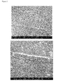
Figure 2 . Observation of the cellular wire. -
Figure 3 . Abundance of filamentous bacteria in 2 week old "electric" sediment. -
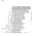
Figure 4 . Phylogeny -
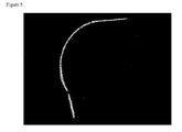
Figure 5 . FISH (Fluorescent In Situ Hybridization). -
Figure 6 . AFM (atomic force microscopy)). -
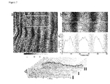
Figure 7 . Investigation of the microbial/cellular cable with electrostatic force microscopy (EFM). -
Figure 8 . TEM (Transmission electron microscopy) image. -
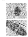
Figure 9 . Transverse (A) and longitudal (B) TEM view of the bacterial/cellular cables. -
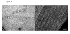
Figure 10 . Negative stain EM on purified subfibre components - The present invention provides electronic conductive materials comprising or consisting of microbial cellular wires and related electronic components and device structures, systems and methods for production and/or assembly. In particular, the invention provides protein-based, naturally conductive cellular wires, which can be used as conductive material without resort to metallization techniques or procedures.
- The present inventors have found that certain bacteria express a plurality of conductive fibres and subfibre filaments. These cells form chains of cells upon growth, and within such a chain of cells, the conductive fibres and subfibre filaments are arranged in parallel in the periplasmic space along the length and around the periphery of said chain of cells. The periplasmic space is the space between the cytoplasmic membrane and the outer membrane, which is seen in all gram-negative bacteria. Preferably, each cell of the cell chain has its own cytoplasmic membrane, while the outer membrane is shared by all cells in a filament, thus allowing the fibres to be isolated from the surroundings.
- The fibres within the cells are conductive, while the outside of the chain of cells is non-conductive. Also, each individual fibre within the cell is conductive inside, but non-conductive on the outside; i.e. the fibres are electrically insulated from other/neighbouring fibres within the cells by invaginations of the outer cell membrane. The cells have been isolated from marine sediment, and it appears that the fact that the cells form long chains of cells allow the cell colony to support electron transfer using the conductive fibres within the cells over longer distances of several centimetres (e.g. 1-15 cm), such as from within an oxygen-deprived marine sediment to the the sediment-water interface. Thus, the fibres are involved in electron transfer reactions across large numbers of cells over relatively long distances of several centimetres. These biologically produced proteinaceous cellular wires could be useful in micro or nanoelectronic applications.
- The invention provides conductive protein-based, nano- or micro-dimensioned wires or conductive components, produced and self-assembled in vitro or in vivo using a native host or engineered microorganisms.
- The terms, "conductive fibres" and "cellular wires" are used interchangeably herein. The chain of bacteria describes above comprises conductive fibres and subfibre filaments, which can be used as wires, e.g. in electronic devices, and such wires are referred to as cellular wires.
- The invention further provides one or more systems or methods for the production and self-assembly of protein-based cellular wires, conductive materials, by the use of microorganisms which can be, optionally, genetically modified to express one or a plurality of conductive fibres and/or subfibre filaments arranged in parallel in the periplasmic space along the length and around the periphery of a chain of cells, wherein the outside of said chain of cells is non-conductive.
- The invention also provides an electronic device structure and/or a circuit or electrical component thereof comprising at least one conductive fibre, subfibre filament or conductive material of the sort described herein, produced and/or self-assembled in vitro or in vivo using the native host or engineered microorganisms.
- Other objects, features, benefits and advantages of the present invention will be apparent from this summary and the following descriptions of certain embodiments, and will be readily apparent to those skilled in the art having knowledge of various parallel conductive fibre-producing microorganisms and similar mechanisms for extracellular electron transfer.
- The present invention relates to conductive fibres, and use thereof in various micro or nanotechnological applications. More specifically, without limitation, the present invention also provides for the culture of bacteria producing a plurality of conductive fibres and/or subfibre filaments arranged in parallel in the periplasmic space along the length and around the periphery of said chain of cells, wherein the outside of said chain of cells is non-conductive. The invention also provides for isolation of such fibres and/or subfibre filaments and, as well as the fabrication of nano-dimensioned electronic circuit components.
- Accordingly, this invention is directed to a method of preparing a conductive electronic circuit component. Such a method can comprise providing a bacterium capable of expressing a conductive proteinaceous fibres and/or subfibre filaments; providing a culture medium conditioned for conductive fibre production, such a medium comprising an electron acceptor; incubating the bacterium and the medium over a time sufficient for fibre and/or subfibre assembly; and isolating conductive fibres and/or subfibre filaments from the medium. In accordance with this invention, conductive fibres and/or subfibre filaments are obtainable from bacterial cells of the present invention. More specifically, without limitation, the gene or genes encoding the conductive proteinaceous fibres and/or subfibre filaments can be isolated and inserted into plasmids or the genome of a recombinant host cell, which cell is then capable of expressing one or more conductive proteinaceous fibres. Such a recombinant microorganism comprising nucleic acid molecules encoding conductive proteinaceous fibres and/or subfibre filaments of the present invention may also be used in the production of a recombinant material of the present invention.
- As described more fully below, the conductive fibres and/or subfibre filaments can be produced and/or obtained from systems comprising one of various strains of the aforementioned fibre-producing species, under appropriate culture conditions, with one or more suitable electron donor components and one or more suitable electron acceptor components, examples of the latter including but not limited to oxygen. Electron acceptors could be any compound, but preferably, the electron acceptor is a soluble/dissolved electron acceptor, such as oxygen and/or nitrate. In one embodiment, it is provided that the electron acceptor is not a solid electron acceptor. A preferred electron acceptor is oxygen. After a time sufficient for adequate protein expression and culture growth, fibres and/or subfibre filaments can be isolated or extracted from the cells, using various techniques known in the art, and used as described elsewhere herein. Conductive fibres and/or subfibre filaments can also be produced and isolated in their soluble form using the native host or engineered microorganisms and assembled as conductive materials into for example electronic components and/or devices in vitro.
- The invention also provides a method of using a cell, preferably a bacterial cell, to prepare an electronic circuit component or electronic device, where that cell express one or more conductive fibres and/or subfibre filaments, which are conductive on the inside and non-conductive on the outside, and when a plurality of fibres and/or subfibre filaments are expressed, the fibres and/or subfibre filaments are arranged in parallel in the periplasmic space along the length and around the periphery of the cell or a chain of cells, wherein the outside of said chain of cells is non-conductive. Such a method can comprise providing at least one Proteobacteria, such as a Deltaproteobacteria, such as a Desulfobacterales, for example a bacteria belonging to the Desulfobulbus genus expressing one or more conductive fibres and/or subfibre filaments, which are conductive on the inside and non-conductive on the outside, and when a plurality of fibres are expressed, the fibres and/or subfibre filaments are arranged in parallel in the periplasmic space along the length and around the periphery of the cell or a chain of cells, wherein the outside of said chain of cells is non-conductive; providing a culture medium conditioned for conductive fibre and/or subfibre filament production, such a medium comprising an electron acceptor; and incubating the bacterium or bacteria in the medium over a time sufficient for fibre formation and/or subfibre filament formation. As described above and illustrated more fully, below, in various embodiments of this invention, such proteinaceous conductive materials can be expressed by various members of the Desulfobulbus genus and/or Desulfobulbaceae family, or by suitable recombinant hosts. In such or certain other embodiments, one or more conductive fibres can be isolated from the medium. If so, such a method can also comprise in vitro circuit assembly. Manifestation of certain embodiments can comprise application of a voltage across one or more fibre and/or subfibre filaments components.
- The invention is also directed to micro and nano-dimensioned electronic device structures, any of which can comprise a conductive circuit component comprising one or more conductive microbial fibres and/or subfibre filaments. Obtainable as described above, and in more detail, below, such components can be contacted with, adsorbed on or applied, connected and/or coupled to a suitable substrate material. A voltage source, alone or together with one or more suitably-dimensioned circuit components, as would be known in the art, can be connected with or coupled to one or more conductive fibres and/or subfibre filaments in the fabrication of a particular device structure.
- A main aspect of the present invention relates to a microorganism, in particular a bacterial cell, which comprises genetic material encoding parallel conductive fibres and/or subfibre filaments located in the periplasmic space along the length and around the periphery of the bacteria. When the cells grow (proliferate), they will tend to grow in a chain, thereby forming a chain of cells. In such a chain of cells, the conductive fibres and/or subfibre filaments are located around the periphery, and run in parallel along the length of the chain of cells, cf. drawings.
Thus, the bacterial cell is able to form a chain of cells upon growth, where the parallel conductive fibres and/or subfibre filaments are located in the periplasmic space along the length and around the periphery of the chain of cells. The invention therefore relates to a bacterial cell, which upon proliferation forms a chain of bacterial cells, said chain comprising a plurality of parallel conductive fibres and/or subfibre filaments located in the periplasmic space along the length and around the periphery of said chain of cells. - The invention also in one aspect relates to a chain of bacterial cells of the invention as defined herein. In this aspect, the invention provides a chain of bacterial cells comprising a plurality of parallel conductive fibres and/or subfibre filaments located in the periplasmic space along the length and around the periphery of said chain of cells, wherein the outside of said chain of cells is non-conductive.
- The conductive fibres and/or subfibre filaments produced by bacterial cells or chain of cells of this invention may be used as conductive fibres and/or subfibre filaments within the cells or they can be extracted from the cells, and used in isolated (non-cellular) form.
- In a preferred embodiment, the outside of the bacterial cell or chain of cells is non-conductive, while the fibres and/or subfibre filaments located inside the cells are conductive. Thus, the conductive fibres and/or subfibre filaments are electrically insulated from the cell surroundings, for example the media or any material used to assemble an electronic device, which incorporate the conductive fibre and/or subfibre material of the invention. Furthermore, each individual conductive fibre and/or subfibre filament located within a cell or chain of cells of the invention preferably comprises an insulating layer, which insulates each conductive fibre from neighbouring parallel conductive fibres. This means that each conductive fibre in the bacterial cell can be used to conduct an individual current, which is separate and different from the currents conducted by parallel fibres of the same chain of cells.
- The bacterial cell or in particular, the chain of bacterial cells of the invention comprises a plurality of individual conductive fibres, such as in the order of 2-40, such as 10-30, such as 15-30, for example 20-25 parallel conductive fibres located in the periplasmic space along the length and around the periphery of said one or more cells or chain of cells. In one particular preferred embodiment, bacterial cell or in particular, the chain of bacterial cells comprises 24 such parallel conductive fibres.
- The diameter of each conductive fibre is within the nanometer scale. In one embodiment, the diameter of a fibre is 10-200 nm, such as 20-190, for example 30-180, such as 40-170, for example 50-160, such as 60-150, for example 70-140, such as 70-130, for example 80-120 nm, such as 85-115, for example 90-110 nm. In a preferred embodiment, the diameter is around 80-120 nm.
- The length of each conductive fibre depends on the length of the chain of bacterial cell. The length of the chain of cells depends on the growth conditions for the cells, and the time allowed for growth. The length of the fibres can be manipulated in order to generate fibres of specific sizes depending on the intended use of the fibres. The chain of bacterial cells can be from µm to cm scale, for example from 1 µm to 10 cm or more. Thus, the length of a conductive fibre of the invention may range from about 3 µm (corresponding to one cell) to 10 cm or more, which corresponds to several ten thousands of cells. Thus, in one embodiment, the conductive fibres are 0.001-10 cm in length, for example 0.01-10 cm, such as 0.05-10 cm, for example 0.1-10 cm, such as 0.2-10, such as 0.3-10, such as 0.4-10, such as 0.5-10, such as 0.6-10, such as 0.7-10, such as 0.8-10, such as 0.9-10, for example 1-10 cm, or 2-9 cm, or 3-9, or 3-8 cm in length.
- Analogously, a chain of bacterial cell of the present invention comprise preferably at least 10 bacterial cells, and may comprise up to several thousand cells, such up to 10,000, for example up to 20,000; 30,000; 40,000; 50,000; 60,000; 70,000; 80,000; 90,000; or 100,000 cells or more. In one embodiment, a chain of cells comprise of 100-200,000 bacterial cells, such as 10-150,000, or 10-100,000 or 10-50,000 cells, such as 20-1000, for example 30-900 cells, such as 40-800, such as 50-700, such as 60-800, such as 70-700, such as 80-700, such as 90-700, such as 100-700, such as 200-700, such as 300-700, such as 400-800, such as 400-700 cells.
- The bacterial cell is in one embodiment a Proteobacteria, such as a Deltaproteobacteria, such as a Desulfobacterales, for example a bacteria belonging to the Desulfobulbus genus. Thus, in one embodiment, the bacterial cell is selected from Proteobacteria. In another embodiment, the bacterial cell is selected from Deltaproteobacteria. In another embodiment, the bacterial cell is selected from Desulfobacterales. In another embodiment, the bacterial cell is selected from Desulfobulbus genus. In one specific embodiment, the bacterial cell is selected from the group consisting of Desulfobulbus elongates, Desulfobulbus japonicas, Desulfobulbus mediterraneus, Desulfobulbus propionicus and Desulfobulbus rhabdoformis. In another specific embodiment, the bacterial cell is selected from the group consisting of Desulfobulbus japonicas, Desulfobulbus mediterraneus and Desulfobulbus rhabdoformis. In one other specific embodiment, the bacterial cell is Desulfobulbus elongates, Desulfobulbus japonicas, Desulfobulbus mediterraneus, Desulfobulbus propionicus or Desulfobulbus rhabdoformis. Also, the chain if cells may comprise a mixture of the bacterial cells mentioned herein above.
- A main object of the present invention is to provide a conductive electronic material of the bacteria of the present invention, in particular a chain of such bacteria as explained herein above. A main aspect of the invention is therefore a conductive material of bacteria, which produce conductive fibres and/or subfibre filaments, which are arranged in parallel inside the cell in the periphery of the cell membrane. The conductive electronic material comprises or consists of one or more conductive fibres of the chain of bacterial cells. The conductive fibres and/or subfibre filaments can be used as conductive fibres within the cells, or they can be extracted from the cells, and used in isolated (non-cellular) form.
The bacterial cells are characterized in that they comprise a plurality of conductive fibres and/or subfibre filaments, which are arranged in parallel in the periplasmic space along the length and around the periphery of the cells. - When the cells grow (proliferate), they will tend to grow in a chain, thereby forming a chain of cells. In such a chain of cells, the conductive fibres and/or subfibre filaments are located around the periphery, and run in parallel along the length of the chain of cells, cf. drawings.
- In a preferred embodiment, the outside of the cells is non-conductive, while the fibres and/or subfibre filaments located inside the cells are conductive, i.e. the conductive fibres and subfibre filaments are insulated by the cell. Thus, the conductive electronic material of the invention is non-conductive on the outside of the cells. Furthermore, each individual conductive fibre preferably comprises an electrically insulating layer, which insulates each conductive fibre from neighbouring parallel conductive fibres. Thus, each conductive fibre and/or subfibre filaments of the conductive material of the present invention is also conductive on the inside, but non-conductive on the outside. This means that each conductive fibre in the bacterial cell can be used to conduct an individual current, which is separate and different from currents conducted by parallel fibres of the same chain of cells.
- The conductive electronic material comprises or consists of a plurality of individual conductive fibres, such as in the order of 2-40, such as 10-30, such as 15-30, for example 20-25 parallel conductive fibres located in the periplasmic space along the length and around the periphery of the chain of cells. In one embodiment, the conductive electronic material comprises or consists of 10, 11, 12, 13, 14, 15, 16, 17, 18, 19, 20, 21, 22, 23, 24, 25, 26, 27, 28, 29 or 30 such parallel conductive fibres. In one particular preferred embodiment, the conductive electronic material comprises or consists of 17 such parallel conductive fibres. Thus, in one embodiment, the conductive electronic material is a conductive fibre, and in another embodiment, the conductive electronic material is a plurality of conductive fibres.
- The diameter and length of each conductive fibre and/or subfibre filaments are described herein above, and may range from 10-200 nm, such as around 80-120 nm in diameter, and 0.0001-10 cm in length.
- The length of the conductive fibres and/or subfibre filaments, which are comprised in the conductive electronic material of the invention, matches the ranges of the lengths of the bacterial chains or fibres. This includes a conductive electronic material of a chain of bacterial cells of the invention, wherein the chain comprise at least 10 bacterial cells, such as 100-50,000 bacterial cells or more.
- However, a specific conductive material where two or more conductive materials of the present invention are assembled may be even longer. Such assemblies comprising multiple conductive materials are also within the scope of the present invention. This includes for example electronic devices comprising conductive materials of the present invention.
- The present invention provides a conductive electronic material comprising or consisting of one or more conductive fibres of a chain of bacterial cells, which comprise a plurality of said conductive fibres and/or subfibre filaments arranged in parallel in the periplasmic space along the length and around the periphery of said chain of cells, wherein the outside of said chain of cells is non-conductive. In one preferred embodiment, the bacterial cells are Proteobacteria, such as a Deltaproteobacteria, such as a Desulfobacterales, for example a bacteria belonging to the Desulfobulbus genus. Thus, in one embodiment, the bacterial cells are selected from Proteobacteria. In another embodiment, the bacterial cells are selected from Deltaproteobacteria. In another embodiment, the bacterial cells are selected from Desulfobacterales. In another embodiment, the bacterial cells are selected from Desulfobulbus genus. In one specific embodiment, the bacterial cells are selected from the group consisting of Desulfobulbus elongates, Desulfobulbus japonicas, Desulfobulbus mediterraneus, Desulfobulbus propionicus and Desulfobulbus rhabdoformis. In another specific embodiment, the bacterial cells are selected from the group consisting of Desulfobulbus japonicas, Desulfobulbus mediterraneus and Desulfobulbus rhabdoformis. In one other specific embodiment, the bacterial cells are Desulfobulbus elongates, Desulfobulbus japonicas, Desulfobulbus mediterraneus, Desulfobulbus propionicus or Desulfobulbus rhabdoformis. Also, the chain if cells may comprise a mixture of the bacterial cells mentioned herein above.
- The conductive electronic material of the invention is produced by a bacterial cell of the invention, and depending on the downstream applications, the conductive electronic material is used while embedded in the chain of bacterial cells. However, in one embodiment, the conductive electronic material is extracted from the cells, such as from the chain of bacterial cells.
- In one aspect, the present invention provides a method of preparing a conductive electronic material as defined herein above. This aspect of the invention provides a method of preparing a conductive electronic material consisting of conductive fibres and/or subfibre filaments, said method comprising
- a) providing bacterial cells capable of forming a plurality of parallel conductive fibres and/or subfibre filaments located in the periplasmic space along the length and around the periphery of the cells, wherein the outside of said cells is non-conductive, and
- b) incubating said bacterial cells in a medium conditioned for conductive fibre formation and/or subfibre filament formation, said medium comprising an electron donor and an electron acceptor, in sufficient time to produce one or more chains of bacterial cells, each chain comprising a plurality of parallel conductive fibres and/or subfibre filaments located in the periplasmic space along the length and around the periphery of said chain of cells.
- A culture medium is selected, which support proliferation of the cells, and which also supports formation of conductive fibres and/or subfibre filaments. The medium should comprise a suitable energy source, and any other required nutrients and additives. In particular, the medium should comprise an electron donor and an electron acceptor. For example, oxygen is used as an electron acceptor. The medium is in one embodiment a gradient culture.
- The chain of bacterial cells produced in step b) may be any of the lengths described above; in one embodiment, the chain comprises at least 10 bacterial cells, but preferably, the chain comprises at least 100 or more. However, the length of the chain depends on the desired length of the conductive fibre material to be obtained by the process.
- In one embodiment, the conductive electronic material, such as the one or more conductive fibre and/or subfibre filament, for example the plurality of parallel conductive fibres, subfibre filaments and/or chain of bacterial cells are isolated from the medium. In one embodiment, the chain of bacterial cells is isolated from the medium. In another embodiment, the conductive electronic material, such as the one or more conductive fibre and/or subfibre filaments, for example the plurality of parallel conductive fibres and/or subfibre filaments is isolated from the one or more chains of bacterial cells.
- The bacterial cells used in this method of the invention are preferably a bacterial cell of the invention, as defined herein above. In one embodiment, the bacterial cells are Proteobacteria, such as a Deltaproteobacteria, such as a Desulfobacterales, for example a bacteria belonging to the Desulfobulbus genus.
- One advantage of the provided method for producing a conductive electronic material is that the method allows mass production of uniform organic microwires and/or cellular wires. The bacterial cells used in the method of the invention also allows the conductive material, such as microwires and/or cellular wires as well as electronic components and devices comprising the conductive material, to be produced by self-organizing, allowing for example the production of growth guided electronic circuits, components or devices.
- The conductive material can be used as components of nano-scale electronics, cf. herein below.
- One aspect of the invention relates to the use of the cells of the invention, in particular bacterial cells and preferably a chain of bacterial cells, as conductive materials. Thus, in one embodiment, the invention provides a use of a chain of bacterial cells comprising a plurality of parallel conductive fibres and/or subfibre filaments located in the periplasmic space along the length and around the periphery of said chain of cells, wherein the outside of said chain of cells is non-conductive, as a conductive material.
- The specific nature and characteristics of the bacterial cells used are defined herein above, and in one embodiment, the bacterial cells are Proteobacteria, such as a Deltaproteobacteria, such as a Desulfobacterales, for example a bacteria belonging to the Desulfobulbus genus.
- In one embodiment, a voltage is applied across said bundle of conductive fibres and/or subfibre filaments.
- The invention also provides electronic components and/or devices, which comprise a conductive material of the invention. Accordingly, the invention also provides electronic devices comprising one or more electronic components of the invention.
- In one aspect, the invention provides an electronic component comprising
- a) a conductive material comprising or consisting of one or more conductive fibres and/or subfibre filaments of a chain of bacterial cells, which comprise a plurality of said conductive fibres and/or subfibre filaments arranged in parallel in the periplasmic space along the length and around the periphery of said chain of cells, wherein the outside of said chain of cells is non-conductive, or
- b) a conductive material prepared by
- i) providing bacterial cells capable of forming a plurality of parallel conductive fibres and/or subfibre filaments located in the periplasmic space along the length and around the periphery of the cells, wherein the outside of said cells is non-conductive, and
- ii) incubating said bacterial cells in a medium conditioned for bacterial proliferation and conductive fibre formation, said medium comprising an electron donor and an electron acceptor, in sufficient time to produce one or more chains of bacterial cells, each chain comprising a plurality of parallel conductive fibres and/or subfibre filaments located in the periplasmic space along the length and around the periphery of said chain of cells. In another aspect, the invention provides an electronic device comprising an electronic component as defined above.
- In a further aspect, the invention provides an electronic device comprising
- a) a conductive material comprising or consisting of one or more conductive fibres of a chain of bacterial cells, which comprise a plurality of said conductive fibres and/or subfibre filaments arranged in parallel in the periplasmic space along the length and around the periphery of said chain of cells, wherein the outside of said chain of cells is non-conductive, or
- b) a conductive material prepared by
- i) providing bacterial cells capable of forming a plurality of parallel conductive fibres and/or subfibre filaments located in the periplasmic space along the length and around the periphery of the cells, wherein the outside of said cells is non-conductive, and
- ii) incubating said bacterial cells in a medium conditioned for bacterial proliferation and conductive fibre formation and/or subfibre filament formation, said medium comprising an electron donor and an electron acceptor, in sufficient time to produce one or more chains of bacterial cells, each chain comprising a plurality of parallel conductive fibres and/or subfibre filaments located in the periplasmic space along the length and around the periphery of said chain of cells.
- Specific embodiments of the conductive materials under a) and b) above are defined elsewhere herein, and also represent specific embodiments of the electronic components and devices of the present invention. For example, the bacterial cell is preferably a Proteobacteria, such as a Deltaproteobacteria, such as a Desulfobacterales, for example a bacteria belonging to the Desulfobulbus genus.
- An electronic component includes any physical entity suitable for use in electronic devices or systems, which entity comprise conductive material. Thus, an electronic component is any physical entity in an electronic device or system used to affect electrons or their associated fields in a desired manner consistent with the intended function of the electronic device or system. Components are generally intended to be connected together, for example by being soldered to a printed circuit board (PCB), to create an electronic circuit with a particular function (for example an amplifier, radio receiver, or oscillator). Components may be packaged singly or in more complex groups as integrated circuits. Some common electronic components are capacitors, inductors, resistors, diodes, transistors, etc. Electronic components are often categorized as active (e.g. transistors and thyristors) or passive (e.g. resistors and capacitors).
- Thus, an electronic component is a basic electronic element that is available in a discrete form (a discrete device or discrete component), and normally has two or more electrical terminals (or leads). These leads connect, usually soldered to a printed circuit board, to create an electronic circuit (a discrete circuit) with a particular function (for example an amplifier, radio receiver, or oscillator). Basic electronic components may be packaged discretely, as arrays or networks of like components, or integrated inside of packages such as semiconductor integrated circuits, hybrid integrated circuits, or thick film devices. The following list illustrates examples of electronic components of the present invention:
Table 1. List of electronic components as examples of components of the invention, which comprise an electronic conductive material of the invention. Terminals and connectors Description Examples Terminal Connector Cable assemblies Cables with connectors or terminals at their ends Power cord Patch cord Test lead Switches Components that can pass current ("closed") or break the flow of current ("open"): Switch Manually operated switch. Electrical description: SPST, SPDT, DPST, DPDT, NPNT (general) Technology: slide switches, toggle switches, rocker switches, rotary switches, pushbutton switches Keypad Array of pushbutton switches DIP switch Small array of switches for internal configuration settings Footswitch Foot-operated switch Knife switch Switch with unenclosed cond uctors Micro switch Mechanically activated switch with snap action Limit switch Mechanically activated switch to sense limit of motion Mercury switch Switch sensing tilt Centrifugal switch Switch sensing centrifugal force due to rate of rotation Relay Electrically operated switch (mechanical, also see Solid State Relay below) Reed switch Magnetically activated switch Thermostat Thermally activated switch Humidistat Humidity activated switch Circuit Breaker Switch opened in response to excessive current: a resettable fuse Resistors Pass current in proportion to voltage (Ohm's law). Resistor - fixed value Power resistor - larger to safely dissipate heat generated SIP or DIP resistor network - array of resistors in one package Variable resistor Rheostat Two terminal variable resistor (often for high power) Potentiometer Three terminal variable resistor (variable voltage divider) Trim pot Small potentiometer, usually for internal adjustments Heater heating element Resistance wire, Nichrome wire wire of high-resistance material, often used as heating element Thermistor temperature-varied resistor Humistor humidity-varied resistor Varistor, Voltage Dependent Resistor, MOV Passes current when excessive voltage present Protection devices Passive components that protect circuits from excessive currents or voltages Fuse over-current protection, one time use Circuit Breaker resettable fuse in the form of a mechanical switch Resettable fuse or PolySwitch circuit breaker action using solid state device Ground-fault protection or residual-current device - circuit breaker sensitive to mains currents passing to ground Metal oxide varistor (MOV), surge absorber, TVS - Over-voltage protection. Inrush current limiter - protection against initial Inrush current Gas discharge tube - protection against high voltage surges Spark gap - electrodes with a gap to arc over at a high voltage Lightning arrester - spark gap used to protect against lightning strikes Capacitors Capacitors store and release electrical charge. They are used for filtering power supply lines, tuning resonant circuits, and for blocking DC voltages while passing AC signals, among numerous other uses. Capacitor fixed capacitance Capacitor network (array) Variable capacitor adjustable capacitance Tuning capacitor - variable capacitor for tuning a radio, oscillator, or tuned circuit Trimmer capacitor - small variable capacitor usually for internal adjustments Varicap diode AC capacitance varies according to the DC voltage applied Magnetic (inductive) devices Electrical components that use magnetism : Inductor, coil, choke Variable inductor Saturable Inductor Transformer Magnetic amplifier (toroid) ferrite impedances, beads Motor / Generator Solenoid speaker / microphone Networks Components that use more than one type of passive component RC network forms an RC circuit, used in snubbers LC Network forms an LC circuit, used in tuneable transformers and RFI filters Piezoelectric devices, crystals, resonators Passive components that use piezoelectric effect Components that use the effect to generate or filter high frequencies Crystal - a ceramic crystal used to generate precise frequencies (See the Modules class below for complete oscillators) Ceramic resonator - a ceramic crystal used to generate semi-precise frequencies Ceramic filter - a ceramic crystal used to filter a band of frequencies such as in radio receivers surface acoustic wave (SAW) filters Components that use the effect as mechanical transducers. Ultrasonic motor - Electric motor that uses the piezoelectric effect For piezo buzzers and microphones, see the Transducer class below Power sources Sources of electrical power Battery acid- or alkali-based power supply Fuel cell an electrochemical generator Power supply usually a mains hook-up Photo voltaic device generates electricity from light Thermo electric generator generates electricity from temperature gradients Electrical generator an electromechanical power source Transducers, sensors, detectors Transducers generate physical effects when driven by an electrical signal, or vice-versa. Sensors (detectors) are transducers that react to environmental conditions by changing their electrical properties or generating an electrical signal. The Transducers listed here are single electronic components (as opposed to complete assemblies), and are passive (see Semiconductors and Tubes for active ones). Only the most common ones are listed here. Audio (see also Piezoelectric devices) Loudspeaker-Magnetic or piezoelectric device to generate full audio Buzzer - Magnetic or piezoelectric sounder to generate tones Position, motion Linear variable differential transformer (LVDT) - Magnetic - detects linear position Rotary encoder, Shaft Encoder - Optical, magnetic, resistive or switches - detects absolute or relative angle or rotational speed Inclinometer - Capacitive - detects angle with respect to gravity Motion sensor, Vibration sensor Flow meter - detects flow in liquid or gas Force, torque Strain gauge - Piezoelectric or resistive - detects squeezing, stretching, twisting Accelerometer - Piezoelectric - detects acceleration, gravity Thermal Thermocouple, thermopile - Wires that generate a voltage proportional to delta temperature Thermistor - Resistor whose resistance changes with temperature, up PTC or down NTC Resistance Temperature Detector (RTD) - Wire whose resistance changes with temperature Bolometer - Device for measuring the power of incident electromagnetic radiation Thermal cutoff - Switch that is opened or closed when a set temperature is exceeded Magnetic field (see also Hall Effect in semiconductors) Magnetometer, Gauss meter Electromagnetic, light Photo resistor - Light dependent resistor (LDR) Semiconductors (Diodes; transistors; Integrated circuits and Optoelectronic devices) Diodes Conduct electricity easily in one direction, among more specific behaviors. Standard Diode, Rectifier, Bridge Rectifier Schottky Diode, Hot Carrier Diode - super fast diode with lower forward voltage drop Zener Diode Passes current in reverse direction to provide a constant voltage reference Transient Voltage Suppression Diode (TVS), Unipolar or Bipolar used to absorb high-voltage spikes Varactor, Tuning diode, Varicap, Variable Capacitance Diode A diode whose AC capacitance varies according to the DC voltage applied. Light Emitting Diode (LED) A diode that emits light LASER Diode A semiconductor laser Photodiode Passes current in proportion to incident light Avalanche Photodiode Photodiode with internal gain Solar Cell, photovoltaic cell, PV array or panel, produces power from light Diode for Alternating Current (DIAC, Trigger Diode, SIDAC) - Often used to trigger an SCR Constant current Diode Peltier cooler A semiconductor heat pump Transistors Active components used for amplification. Bipolar transistors Bipolar Junction Transistor (BJT, or simply "transistor") - NPN or PNP - Photo transistor - Amplified photodetector Darlington transistor - NPN or PNP - Photo Darlington - Amplified photodetector Sziklai pair (Compound transistor, complementary Darlington) Field effect transistor (FET) Junction Field Effect Transistor (JFET) - N-CHANNEL or P-CHANNEL Metal Oxide Semiconductor FET (MOSFET) - N-CHANNEL or P-CHANNEL MEtal Semiconductor FET (MESFET) High Electron Mobility Transistor (HEMT) Thyristors Silicon Controlled Rectifier (SCR) - Passes current only after triggered by a sufficient control voltage on its gate TRIode for Alternating Current (TRIAC) - Bidirectional SCR UniJunction Transistor (UJT) Programmable UniJunction Transistor (PUT) Static Induction Transistor/Thyristor (SIT, SITh) Composite transistors Insulated Gate Bipolar Transistor (IGBT) Integrated circuits Digital Analog Hall effect sensor - Senses a magnetic field Current sensor - Senses a current through it Optoelectronic devices Optoelectronics Opto-Isolator, Opto-Coupler, Photo-Coupler - Photodiode, BJT, JFET, SCR, TRIAC, Zero-crossing TRIAC, Open collector IC, CMOS IC, Solid State Relay (SSR) Opto Switch, Opto Interrupter, Optical Switch, Optical Interrupter, Photo switch, Photo Interrupter LED Display - Sevensegment display, Sixteen-segment display, Dot matrix display Display technologies Current Filament lamp (indicator lamp) Vacuum fluorescent display (VFD) (preformed characters, 7 segment, starburst) Cathode ray tube (CRT) (dot matrix scan (e.g. computer monitor), radial scan (e.g. radar), arbitrary scan (e.g. oscilloscope)) (monochrome & colour) LCD (preformed characters, dot matrix) (passive, TFT) (monochrome, colour) Neon (individual, 7 segment display) LED (individual, 7 segment display, starburst display, dot matrix) Flap indicator (numeric, preprinted messages) Plasma display (dot matrix) Obsolete: Filament lamp 7 segment display (aka 'minitron') Nixie Tube Dekatron (aka glow transfer tube) Magic eye tube indicator Penetron (a 2 colour see-through CRT) Vacuum tubes (Valves) Based on current conduction through a vacuum (see Vacuum tube) Diode or Rectifier tube Amplifying tubes Triode Tetrode Pentode Hexode Pentagrid Octode Microwave tubes: Klystron, Magnetron or Traveling-wave tube Optical detectors or emitters Phototube or Photodiode - tube equivalent of semiconductor photodiode Photomultiplier tube - Phototube with internal gain Cathode ray tube (CRT) or Television picture tube Vacuum fluorescent display (VFD) - Modern non-raster sort of small CRT display Magic eye tube - Small CRT display used as a tuning meter (obsolete) X-ray tube - Produces x-rays Discharge devices Gas discharge tube Obsolete: Mercury arc rectifier Voltage regulator tube Nixie tube Thyratron Ignitron Antennas Antennas transmit or receive radio waves Elemental dipole Yagi Phased array Loop antenna Parabolic dish Log-periodic dipole array Biconical Feedhorn Assemblies, modules Multiple electronic components assembled in a device that is in itself used as a component Oscillator Display devices Liquid crystal display (LCD) Digital voltmeters Filter Prototyping aids Wire-wrap Breadboard Mechanical accessories Enclosure (electrical) Heat sink Fan Other Printed circuit boards Lamp Waveguide Memristor Obsolete Carbon amplifier (see Carbon microphones used as amplifiers) Carbon arc (negative resistance device) Dynamo (historic rf generator) - The electronic components and devices of the invention may be used in any type of electrical system, which requires the use of conductive materials. In one preferred embodiment, the electronic component and/or device is microstructured or nanostructured.
- The conductive fibres and/or subfibre filaments of the invention may be used as a single strand wire. However, the fibres may also be used as a bundle of wires, a multistranded wire, i.e. as a cable. This cellular wire and/or cable may be used to carry electricity and telecommunications signals. Thus, wires and cables of the invention may be used in telephone and data cables, and as conductors in electric power transmission, and heating.
- In particular, the conductive fibres, conductive material, components and devices of the invention are environmental friendly and non-toxic to human and animals, which is a significant advantage of these products. Thus, the conductive fibres, conductive material, components and devices of the invention can be used in edible and biodegradeable circuits and biosensors, for example for application in foods, and incorporation in the body of human and animals, as well as environmental sensor. The conductive fibres, conductive material, components and devices also provides soft and flexible electronics, which is advantageous in many applications, for example in devices for invasive medical use. Also miniaturization of biosensors based on chemioluminescense can be achieved by these conductive products of the invention.
- The conductive fibres, conductive material, components and devices of the invention are also usable in connection with energy supply or electron exchange in biosensors or micro bioreactors (feeding or draining electrons is a "clean" way to drive reduction or oxidation processes).
- The conductive fibres, conductive material, components and devices of the invention are also allows the production of devices for enhanced oxidative bioremediation of less mobile contaminants in subsurface matrix.
- The products can also be used for remote control of biomineralization and microbial nanoparticle generation.
-
Figures 1-10 illustrates specific embodiments of the present invention. -
Figure 1 . Demonstration of electric grids in marine sediment. Porewater profiles of pH, hydrogen sulphide and oxygen in harbor sediment (a & b) and bay sediment (e & f) after about 3 weeks incubation with oxygen present in the overlying water. The vertical separation of oxygen and free hydrogen sulphide and the pH peak in the oxic zone could only be explained by the presence of centimeter long electric conductors transferring electrons from sulfide oxidation to oxygen reduction. Minimum current densities for the harbor and bay sediment were found to be 86 and 14 mA pr meter square, respectively (see Nielsen et al 2010 for details). Subsequent experiments with sediment confirmed the construction of an electric grid depending on vertical growth or migration of bacteria: Currents stopped if the conductors were cut by passing a thin wire through the sediment, and horizontal filters imbedded in the sediment could prevent the formation of an electric grid, only if the pore width was below typical bacterial cell diameter (0.8 micrometer). -
Figure 2 . Observation of the cellular wire. Layers of washed glass beads were incubated with sulfidic sediment below and oxic sediment above, and electric currents were found to be established through the glass layer after 3 weeks. The beads were inspected with scanning electron microscopy (SEM) for possible conductive structures. Long filamentous bacteria were found to abound (a) and a closer view revealed uniform fibers or ridges running along the filaments with no interruptions at the cell junctions (b). These observations are in support that the bacteria serve as living electric cables holding a bunch of conductive fibers. -
Figure 3 . Abundance of filamentous bacteria in 2 week old "electric" sediment with oxygen penetration to 1.5 mm depth and detectable hydrogen sulfide is seen only at depths below 9 mm. Only filaments without sulfur and about 1 micrometer wide were recorded. Pretreatment and incubation of sulfidic sediment were performed as described in Nielsen et al. (2010), and filament density was measured by counting filament intercepts with search lines in subsamples inspected by light microscopy (Leica Apotome, 200 X, phase contrast). The distribution of bacterial filaments aligned very well with the electric zone read from the chemical profiles, and integrated with depth these microbial cellular wires amounted to about 6000 kilometers per square meter -
Figure 4 . Sequencing of 16sDNA from bacteria in the electric zone showed high enrichment of several species of the family Desulfobulbaceae with Desulfobulbus propionicus as their closest, cultivated relative. As judged from the genetic distances, the detected electric zone species may appear to form a genus of their own -
Figure 5 . FISH (Fluorescent In Situ Hybridization) with a specific probe confirmed that the observed filaments (Figure 2 and3 ) were indeed the Desulfobulbacea species found by sequencing (Figure 4 ).. A new probe targeting specifically the electric cable group of Desulfobulbaceae has now been developed as a tool for rapid screening and quantification in cultures and enrichments. -
Figure 6 . AFM (atomic force microscopy) investigation of the ridges running continuous from cell to cell of the bacterial filaments. A. Topographic transect across one filament showing that the ridges are well separated and have a uniform width of about 120 nanometer B. An AFM picture of a chain of cells forming a cable. At the cell-cell junction, a 700x700 nm square subsection is shown, which is enlarged in C (phase contrast) and D (amplitude). -
Figure 7 . Investigation of the microbial/cellular cable with electrostatic force microscopy (EFM) revealed exceptionally high contrasting charge distribution for a biological material, suggesting the presence of electron conductors within the ridges. A: Charge distribution on the surface of a filament after all topographic effects have been filtered out. B and C: Close up of the insert in A showing the distinct separation of about 100 nm wide conductive bands with about 20 nm wide spacers in between. D: Longitudal records of along the lines marked in A showing continuity of charge distribution across the cell-cell junction. -
Figure 8 . TEM (Transmission electron microscopy) image with crossection of 9 bacterial/cellular cables with sediment material around. They form two distinct groups probably representing species; small ones (- 400 nm 0) having exactly 15 periferal ridges and large ones (- 700 nm 0) having 17 ridges.. -
Figure 9 . Transverse (A) and longitudal (B) TEM view of the bacterial/cellular cables. The ridges seemed to be composed of a uniform material separated from the cell interior by the cytoplasmic membrane and from the outside and adjacent ridges by the outer membrane. The material is thus situated in the periplasmic space and supposed to be the conductive fibers of the bacterial cable. An open space between cells was bridged by the fibers and the deflated outer membrane which therefore represented an emergent property of the whole, multicellular bacterium. The insulating effect of the outer membrane can explain why it so far have been impossible to record electronic properties of the filaments by applying metal electrodes on them. -
Figure 10 . Negative stain EM on purified subfibre components showing individual -7 nm subfibre filaments and intertwined -7 nm subfibre filaments forming higher oligomers. B, Negative stain EM of a bacterial cable cell. Arrows indicate areas where it can be seen that -7 nm fragments run along/inside larger fibres having a size of approximately 80 nm.
Claims (15)
- A conductive electronic material comprising or consisting of one or more conductive fibres and/or subfibre filaments of a chain of bacterial cells, which comprise a plurality of said conductive fibres and/or subfibre filaments arranged in parallel in the periplasmic space along the length and around the periphery of said chain of cells, wherein the outside of said chain of cells is non-conductive.
- The conductive electronic material of claim 1, wherein each conductive fibre and/or subfibre filament comprise an insulating layer, which insulate each conductive fibre from neighbouring parallel conductive fibres.
- The conductive electronic material of any of the preceding claims, wherein said bacterial cells form one or more chains of at least 10 bacterial cells, such as a chain of 100-50,000 bacterial cells or more.
- The conductive electronic material of any of the preceding claims, wherein said conductive material comprises or consists of 2-40, such as 10-30, such as 15-30, for example 20-25, such as 24 parallel conductive fibres and/or subfibre filaments located in the periplasmic space along the length and around the periphery of said chain of cells.
- The conductive electronic material of any of the preceding claims, wherein said bacterial cell is a Proteobacteria, such as a Deltaproteobacteria, such as a Desulfobacterales, for example a bacteria belonging to the Desulfobulbus genus
- The conductive electronic material of any of the preceding claims, wherein said conductive material is extracted from said chain of bacterial cells.
- A method of preparing a conductive electronic material consisting of conductive fibres and/or subfibre filaments, said method comprisinga) providing bacterial cells capable of forming a plurality of parallel conductive fibres and/or subfibre filaments located in the periplasmic space along the length and around the periphery of the cells, wherein the outside of said cells is non-conductive, andb) incubating said bacterial cells in a medium conditioned for bacterial proliferation and conductive fibre formation and/or subfibre filament formation, said medium comprising an electron donor and an electron acceptor, in sufficient time to produce one or more chains of bacterial cells, each chain comprising a plurality of parallel conductive fibres and/or subfibre filaments located in the periplasmic space along the length and around the periphery of said chain of cells.
- The method of claim 7, wherein said medium is a gradient culture.
- The method of any of claims 7-8, wherein said plurality of parallel conductive fibres, subfibre filaments and/or chain of bacterial cells is isolated from the medium.
- The method of any of claims 7-9, wherein said bacterial cells are Proteobacteria, such as a Deltaproteobacteria, such as a Desulfobacterales, for example bacteria belonging to the Desulfobulbus genus.
- Use of a chain of bacterial cells comprising a plurality of parallel conductive fibres and/or subfibre filaments located in the periplasmic space along the length and around the periphery of said chain of cells, wherein the outside of said chain of cells is non-conductive, as a conductive material.
- The use according to claim 11, wherein said bacterial cells are Proteobacteria, such as a Deltaproteobacteria, such as a Desulfobacterales, for example a bacteria belonging to the Desulfobulbus genus.
- An electronic device or component comprisinga) a conductive material as defined in any of claims 1 to 6, orb) a conductive material produced as defined an any of claims 7 to 10
- A chain of bacterial cells comprising a plurality of parallel conductive fibres and/or subfibre filaments located in the periplasmic space along the length and around the periphery of said chain of cells, wherein the outside of said chain of cells is non-conductive.
- A bacterial cell, which upon proliferation forms a chain of bacterial cells comprising a plurality of parallel conductive fibres and/or subfibre filaments located in the periplasmic space along the length and around the periphery of said chain of cells, wherein the outside of said chain of cells is non-conductive.
Applications Claiming Priority (1)
| Application Number | Priority Date | Filing Date | Title |
|---|---|---|---|
| DKPA201270169 | 2012-04-03 |
Publications (2)
| Publication Number | Publication Date |
|---|---|
| EP2647727A1 true EP2647727A1 (en) | 2013-10-09 |
| EP2647727B1 EP2647727B1 (en) | 2017-11-01 |
Family
ID=48087398
Family Applications (1)
| Application Number | Title | Priority Date | Filing Date |
|---|---|---|---|
| EP13162128.6A Active EP2647727B1 (en) | 2012-04-03 | 2013-04-03 | Bacterial conductive fibres |
Country Status (2)
| Country | Link |
|---|---|
| EP (1) | EP2647727B1 (en) |
| DK (1) | DK2647727T3 (en) |
Cited By (2)
| Publication number | Priority date | Publication date | Assignee | Title |
|---|---|---|---|---|
| EP3543342A1 (en) | 2018-03-19 | 2019-09-25 | Universiteit Antwerpen | Isolated microbial conductive fiber material |
| CN112816528A (en) * | 2021-02-01 | 2021-05-18 | 合肥艾创微电子科技有限公司 | Perception storage integrated bionic tactile fiber and preparation method thereof |
Citations (1)
| Publication number | Priority date | Publication date | Assignee | Title |
|---|---|---|---|---|
| US20120053320A1 (en) * | 2010-08-30 | 2012-03-01 | Gemma Reguera | Microbial nanowires and methods of making and using same |
-
2013
- 2013-04-03 EP EP13162128.6A patent/EP2647727B1/en active Active
- 2013-04-03 DK DK13162128.6T patent/DK2647727T3/en active
Patent Citations (1)
| Publication number | Priority date | Publication date | Assignee | Title |
|---|---|---|---|---|
| US20120053320A1 (en) * | 2010-08-30 | 2012-03-01 | Gemma Reguera | Microbial nanowires and methods of making and using same |
Non-Patent Citations (7)
| Title |
|---|
| CHILDERS, S. E.; CIUFO, S.; LOVLEY, D. R.: "Geobacter metallireducens accesses insoluble Fe(III) oxide by chemotaxis", NATURE, vol. 416, 2002, pages 767 - 769 |
| CHRISTIAN PFEFFER ET AL: "Filamentous bacteria transport electrons over centimetre distances", NATURE, vol. 491, no. 7423, 24 October 2012 (2012-10-24), pages 218 - 221, XP055072341, ISSN: 0028-0836, DOI: 10.1038/nature11586 * |
| D. E. HOLMES ET AL: "Electron Transfer by Desulfobulbus propionicus to Fe(III) and Graphite Electrodes", APPLIED AND ENVIRONMENTAL MICROBIOLOGY, vol. 70, no. 2, 1 February 2004 (2004-02-01), pages 1234 - 1237, XP055072440, ISSN: 0099-2240, DOI: 10.1128/AEM.70.2.1234-1237.2004 * |
| GEMMA REGUERA ET AL: "Extracellular electron transfer via microbial nanowires", NATURE, vol. 435, no. 7045, 23 June 2005 (2005-06-23), pages 1098 - 1101, XP055037329, ISSN: 0028-0836, DOI: 10.1038/nature03661 * |
| GEMMA REGUERA: "Microbiology: Bacterial power cords", NATURE, vol. 491, no. 7423, 24 October 2012 (2012-10-24), pages 201 - 202, XP055072360, ISSN: 0028-0836, DOI: 10.1038/nature11638 * |
| JOSHUA VEAZEY ET AL: "Electronic properties of conductive pili of the metal-reducing bacterium Geobacter sulfurreducens probed by scanning tunneling microscopy", PHYSICAL REVIEW E, vol. 84, no. 6, 1 December 2011 (2011-12-01), pages 1 - 4, XP055047692, ISSN: 1539-3755, DOI: 10.1103/PhysRevE.84.060901 * |
| LARS PETER NIELSEN ET AL: "Electric currents couple spatially separated biogeochemical processes in marine sediment", NATURE, vol. 463, no. 7284, 25 February 2010 (2010-02-25), pages 1071 - 1074, XP055072372, ISSN: 0028-0836, DOI: 10.1038/nature08790 * |
Cited By (3)
| Publication number | Priority date | Publication date | Assignee | Title |
|---|---|---|---|---|
| EP3543342A1 (en) | 2018-03-19 | 2019-09-25 | Universiteit Antwerpen | Isolated microbial conductive fiber material |
| CN112816528A (en) * | 2021-02-01 | 2021-05-18 | 合肥艾创微电子科技有限公司 | Perception storage integrated bionic tactile fiber and preparation method thereof |
| CN112816528B (en) * | 2021-02-01 | 2024-04-09 | 合肥艾创微电子科技有限公司 | A perception storage integrated bionic tactile fiber and preparation method thereof |
Also Published As
| Publication number | Publication date |
|---|---|
| EP2647727B1 (en) | 2017-11-01 |
| DK2647727T3 (en) | 2018-02-05 |
Similar Documents
| Publication | Publication Date | Title |
|---|---|---|
| Li et al. | 1D piezoelectric material based nanogenerators: methods, materials and property optimization | |
| Zhou et al. | Flexible piezotronic strain sensor | |
| Riaz et al. | Study of the piezoelectric power generation of ZnO nanowire arrays grown by different methods | |
| Hsu et al. | Vertical p-type Cu-doped ZnO/n-type ZnO homojunction nanowire-based ultraviolet photodetector by the furnace system with hotwire assistance | |
| CN101409961B (en) | Surface heat light source, its preparation method and its application method for heating objects | |
| Pearton et al. | The promise and perils of wide‐bandgap semiconductor nanowires for sensing, electronic, and photonic applications | |
| JP5860350B2 (en) | Polymer composite piezoelectric body and piezoelectric element using the same | |
| Johar et al. | Facile growth of high aspect ratio c-axis GaN nanowires and their application as flexible pn NiO/GaN piezoelectric nanogenerators | |
| Omar et al. | Investigation on dielectric constant of zinc oxide | |
| EP2647727B1 (en) | Bacterial conductive fibres | |
| Tao et al. | Single-dislocation Schottky diodes | |
| Zhang et al. | Improvement in the Piezoelectric Performance of a ZnO Nanogenerator by a ZnO/Spiro‐MeOTAD ps‐n Heterojunction | |
| Feng et al. | Electronic structure and energy band of IIIA doped group ZnO nanosheets | |
| Lungu | Effects of dopants and processing parameters on the properties of ZnO-V2O5-based varistors prepared by powder metallurgy: a review | |
| Matsuura et al. | Anomalous temperature dependence of the hall coefficient of heavily Al-doped 4H-SiC epilayers in the band conduction region | |
| Soomro et al. | Piezoelectric power generation from zinc oxide nanowires grown on paper substrate | |
| Shiomi et al. | Giant piezoelectric response in superionic polar semiconductor | |
| Haq et al. | GGA+ U investigations of impurity d-electrons effects on the electronic and magnetic properties of ZnO | |
| CN103325942B (en) | Ferroelectric tunnel junction device | |
| Liu et al. | Novel ZnO Nanorod Flexible Strain Sensor and Strain Driving Transistor with an Ultrahigh 107 Scale “On”−“Off” Ratio Fabricated by a Single-Step Hydrothermal Reaction | |
| CN110838519B (en) | Flexible ZnO/NiO/ZnO multifunctional triode and preparation method thereof | |
| Amin et al. | Current‐transport studies and trap extraction of hydrothermally grown ZnO nanotubes using gold Schottky diode | |
| Pandey et al. | Properties and applications of varistor–transistor hybrid devices | |
| Sun et al. | Growth of ultralong ZnO microwire and its application in isolatable and flexible piezoelectric strain sensor | |
| US9455399B2 (en) | Growth of antimony doped P-type zinc oxide nanowires for optoelectronics |
Legal Events
| Date | Code | Title | Description |
|---|---|---|---|
| PUAI | Public reference made under article 153(3) epc to a published international application that has entered the european phase |
Free format text: ORIGINAL CODE: 0009012 |
|
| AK | Designated contracting states |
Kind code of ref document: A1 Designated state(s): AL AT BE BG CH CY CZ DE DK EE ES FI FR GB GR HR HU IE IS IT LI LT LU LV MC MK MT NL NO PL PT RO RS SE SI SK SM TR |
|
| AX | Request for extension of the european patent |
Extension state: BA ME |
|
| 17P | Request for examination filed |
Effective date: 20140409 |
|
| RBV | Designated contracting states (corrected) |
Designated state(s): AL AT BE BG CH CY CZ DE DK EE ES FI FR GB GR HR HU IE IS IT LI LT LU LV MC MK MT NL NO PL PT RO RS SE SI SK SM TR |
|
| 17Q | First examination report despatched |
Effective date: 20151113 |
|
| GRAP | Despatch of communication of intention to grant a patent |
Free format text: ORIGINAL CODE: EPIDOSNIGR1 |
|
| RIC1 | Information provided on ipc code assigned before grant |
Ipc: B82Y 5/00 20110101ALI20170407BHEP Ipc: C12R 1/01 20060101AFI20170407BHEP Ipc: C12N 1/20 20060101ALI20170407BHEP |
|
| INTG | Intention to grant announced |
Effective date: 20170515 |
|
| GRAS | Grant fee paid |
Free format text: ORIGINAL CODE: EPIDOSNIGR3 |
|
| GRAA | (expected) grant |
Free format text: ORIGINAL CODE: 0009210 |
|
| AK | Designated contracting states |
Kind code of ref document: B1 Designated state(s): AL AT BE BG CH CY CZ DE DK EE ES FI FR GB GR HR HU IE IS IT LI LT LU LV MC MK MT NL NO PL PT RO RS SE SI SK SM TR |
|
| REG | Reference to a national code |
Ref country code: GB Ref legal event code: FG4D |
|
| REG | Reference to a national code |
Ref country code: CH Ref legal event code: EP Ref country code: AT Ref legal event code: REF Ref document number: 942097 Country of ref document: AT Kind code of ref document: T Effective date: 20171115 |
|
| REG | Reference to a national code |
Ref country code: IE Ref legal event code: FG4D |
|
| REG | Reference to a national code |
Ref country code: DE Ref legal event code: R096 Ref document number: 602013028634 Country of ref document: DE |
|
| REG | Reference to a national code |
Ref country code: DK Ref legal event code: T3 Effective date: 20180201 |
|
| REG | Reference to a national code |
Ref country code: NL Ref legal event code: FP |
|
| REG | Reference to a national code |
Ref country code: LT Ref legal event code: MG4D |
|
| REG | Reference to a national code |
Ref country code: AT Ref legal event code: MK05 Ref document number: 942097 Country of ref document: AT Kind code of ref document: T Effective date: 20171101 |
|
| REG | Reference to a national code |
Ref country code: FR Ref legal event code: PLFP Year of fee payment: 6 |
|
| PG25 | Lapsed in a contracting state [announced via postgrant information from national office to epo] |
Ref country code: LT Free format text: LAPSE BECAUSE OF FAILURE TO SUBMIT A TRANSLATION OF THE DESCRIPTION OR TO PAY THE FEE WITHIN THE PRESCRIBED TIME-LIMIT Effective date: 20171101 Ref country code: FI Free format text: LAPSE BECAUSE OF FAILURE TO SUBMIT A TRANSLATION OF THE DESCRIPTION OR TO PAY THE FEE WITHIN THE PRESCRIBED TIME-LIMIT Effective date: 20171101 Ref country code: NO Free format text: LAPSE BECAUSE OF FAILURE TO SUBMIT A TRANSLATION OF THE DESCRIPTION OR TO PAY THE FEE WITHIN THE PRESCRIBED TIME-LIMIT Effective date: 20180201 Ref country code: SE Free format text: LAPSE BECAUSE OF FAILURE TO SUBMIT A TRANSLATION OF THE DESCRIPTION OR TO PAY THE FEE WITHIN THE PRESCRIBED TIME-LIMIT Effective date: 20171101 Ref country code: ES Free format text: LAPSE BECAUSE OF FAILURE TO SUBMIT A TRANSLATION OF THE DESCRIPTION OR TO PAY THE FEE WITHIN THE PRESCRIBED TIME-LIMIT Effective date: 20171101 |
|
| PG25 | Lapsed in a contracting state [announced via postgrant information from national office to epo] |
Ref country code: RS Free format text: LAPSE BECAUSE OF FAILURE TO SUBMIT A TRANSLATION OF THE DESCRIPTION OR TO PAY THE FEE WITHIN THE PRESCRIBED TIME-LIMIT Effective date: 20171101 Ref country code: LV Free format text: LAPSE BECAUSE OF FAILURE TO SUBMIT A TRANSLATION OF THE DESCRIPTION OR TO PAY THE FEE WITHIN THE PRESCRIBED TIME-LIMIT Effective date: 20171101 Ref country code: BG Free format text: LAPSE BECAUSE OF FAILURE TO SUBMIT A TRANSLATION OF THE DESCRIPTION OR TO PAY THE FEE WITHIN THE PRESCRIBED TIME-LIMIT Effective date: 20180201 Ref country code: HR Free format text: LAPSE BECAUSE OF FAILURE TO SUBMIT A TRANSLATION OF THE DESCRIPTION OR TO PAY THE FEE WITHIN THE PRESCRIBED TIME-LIMIT Effective date: 20171101 Ref country code: AT Free format text: LAPSE BECAUSE OF FAILURE TO SUBMIT A TRANSLATION OF THE DESCRIPTION OR TO PAY THE FEE WITHIN THE PRESCRIBED TIME-LIMIT Effective date: 20171101 Ref country code: GR Free format text: LAPSE BECAUSE OF FAILURE TO SUBMIT A TRANSLATION OF THE DESCRIPTION OR TO PAY THE FEE WITHIN THE PRESCRIBED TIME-LIMIT Effective date: 20180202 Ref country code: IS Free format text: LAPSE BECAUSE OF FAILURE TO SUBMIT A TRANSLATION OF THE DESCRIPTION OR TO PAY THE FEE WITHIN THE PRESCRIBED TIME-LIMIT Effective date: 20180301 |
|
| PG25 | Lapsed in a contracting state [announced via postgrant information from national office to epo] |
Ref country code: SK Free format text: LAPSE BECAUSE OF FAILURE TO SUBMIT A TRANSLATION OF THE DESCRIPTION OR TO PAY THE FEE WITHIN THE PRESCRIBED TIME-LIMIT Effective date: 20171101 Ref country code: CZ Free format text: LAPSE BECAUSE OF FAILURE TO SUBMIT A TRANSLATION OF THE DESCRIPTION OR TO PAY THE FEE WITHIN THE PRESCRIBED TIME-LIMIT Effective date: 20171101 Ref country code: CY Free format text: LAPSE BECAUSE OF FAILURE TO SUBMIT A TRANSLATION OF THE DESCRIPTION OR TO PAY THE FEE WITHIN THE PRESCRIBED TIME-LIMIT Effective date: 20171101 Ref country code: EE Free format text: LAPSE BECAUSE OF FAILURE TO SUBMIT A TRANSLATION OF THE DESCRIPTION OR TO PAY THE FEE WITHIN THE PRESCRIBED TIME-LIMIT Effective date: 20171101 |
|
| REG | Reference to a national code |
Ref country code: DE Ref legal event code: R097 Ref document number: 602013028634 Country of ref document: DE |
|
| PG25 | Lapsed in a contracting state [announced via postgrant information from national office to epo] |
Ref country code: IT Free format text: LAPSE BECAUSE OF FAILURE TO SUBMIT A TRANSLATION OF THE DESCRIPTION OR TO PAY THE FEE WITHIN THE PRESCRIBED TIME-LIMIT Effective date: 20171101 Ref country code: SM Free format text: LAPSE BECAUSE OF FAILURE TO SUBMIT A TRANSLATION OF THE DESCRIPTION OR TO PAY THE FEE WITHIN THE PRESCRIBED TIME-LIMIT Effective date: 20171101 Ref country code: PL Free format text: LAPSE BECAUSE OF FAILURE TO SUBMIT A TRANSLATION OF THE DESCRIPTION OR TO PAY THE FEE WITHIN THE PRESCRIBED TIME-LIMIT Effective date: 20171101 Ref country code: RO Free format text: LAPSE BECAUSE OF FAILURE TO SUBMIT A TRANSLATION OF THE DESCRIPTION OR TO PAY THE FEE WITHIN THE PRESCRIBED TIME-LIMIT Effective date: 20171101 |
|
| PLBE | No opposition filed within time limit |
Free format text: ORIGINAL CODE: 0009261 |
|
| STAA | Information on the status of an ep patent application or granted ep patent |
Free format text: STATUS: NO OPPOSITION FILED WITHIN TIME LIMIT |
|
| 26N | No opposition filed |
Effective date: 20180802 |
|
| PGFP | Annual fee paid to national office [announced via postgrant information from national office to epo] |
Ref country code: IE Payment date: 20180706 Year of fee payment: 6 |
|
| PG25 | Lapsed in a contracting state [announced via postgrant information from national office to epo] |
Ref country code: SI Free format text: LAPSE BECAUSE OF FAILURE TO SUBMIT A TRANSLATION OF THE DESCRIPTION OR TO PAY THE FEE WITHIN THE PRESCRIBED TIME-LIMIT Effective date: 20171101 Ref country code: MC Free format text: LAPSE BECAUSE OF FAILURE TO SUBMIT A TRANSLATION OF THE DESCRIPTION OR TO PAY THE FEE WITHIN THE PRESCRIBED TIME-LIMIT Effective date: 20171101 |
|
| REG | Reference to a national code |
Ref country code: CH Ref legal event code: PL |
|
| PG25 | Lapsed in a contracting state [announced via postgrant information from national office to epo] |
Ref country code: LU Free format text: LAPSE BECAUSE OF NON-PAYMENT OF DUE FEES Effective date: 20180403 |
|
| PG25 | Lapsed in a contracting state [announced via postgrant information from national office to epo] |
Ref country code: CH Free format text: LAPSE BECAUSE OF NON-PAYMENT OF DUE FEES Effective date: 20180430 Ref country code: LI Free format text: LAPSE BECAUSE OF NON-PAYMENT OF DUE FEES Effective date: 20180430 |
|
| PG25 | Lapsed in a contracting state [announced via postgrant information from national office to epo] |
Ref country code: MT Free format text: LAPSE BECAUSE OF NON-PAYMENT OF DUE FEES Effective date: 20180403 |
|
| PG25 | Lapsed in a contracting state [announced via postgrant information from national office to epo] |
Ref country code: TR Free format text: LAPSE BECAUSE OF FAILURE TO SUBMIT A TRANSLATION OF THE DESCRIPTION OR TO PAY THE FEE WITHIN THE PRESCRIBED TIME-LIMIT Effective date: 20171101 |
|
| PG25 | Lapsed in a contracting state [announced via postgrant information from national office to epo] |
Ref country code: IE Free format text: LAPSE BECAUSE OF NON-PAYMENT OF DUE FEES Effective date: 20190403 |
|
| PG25 | Lapsed in a contracting state [announced via postgrant information from national office to epo] |
Ref country code: PT Free format text: LAPSE BECAUSE OF FAILURE TO SUBMIT A TRANSLATION OF THE DESCRIPTION OR TO PAY THE FEE WITHIN THE PRESCRIBED TIME-LIMIT Effective date: 20171101 Ref country code: HU Free format text: LAPSE BECAUSE OF FAILURE TO SUBMIT A TRANSLATION OF THE DESCRIPTION OR TO PAY THE FEE WITHIN THE PRESCRIBED TIME-LIMIT; INVALID AB INITIO Effective date: 20130403 |
|
| PG25 | Lapsed in a contracting state [announced via postgrant information from national office to epo] |
Ref country code: MK Free format text: LAPSE BECAUSE OF NON-PAYMENT OF DUE FEES Effective date: 20171101 |
|
| PG25 | Lapsed in a contracting state [announced via postgrant information from national office to epo] |
Ref country code: AL Free format text: LAPSE BECAUSE OF FAILURE TO SUBMIT A TRANSLATION OF THE DESCRIPTION OR TO PAY THE FEE WITHIN THE PRESCRIBED TIME-LIMIT Effective date: 20171101 |
|
| REG | Reference to a national code |
Ref country code: FR Ref legal event code: PLFP Year of fee payment: 11 |
|
| PGFP | Annual fee paid to national office [announced via postgrant information from national office to epo] |
Ref country code: DE Payment date: 20250321 Year of fee payment: 13 |
|
| PGFP | Annual fee paid to national office [announced via postgrant information from national office to epo] |
Ref country code: DK Payment date: 20250408 Year of fee payment: 13 |
|
| PGFP | Annual fee paid to national office [announced via postgrant information from national office to epo] |
Ref country code: FR Payment date: 20250408 Year of fee payment: 13 |
|
| PGFP | Annual fee paid to national office [announced via postgrant information from national office to epo] |
Ref country code: GB Payment date: 20260326 Year of fee payment: 14 |
|
| PGFP | Annual fee paid to national office [announced via postgrant information from national office to epo] |
Ref country code: BE Payment date: 20260324 Year of fee payment: 14 |
|
| PGFP | Annual fee paid to national office [announced via postgrant information from national office to epo] |
Ref country code: NL Payment date: 20260326 Year of fee payment: 14 |