EP2645599A1 - Flexible Optimization of the Signal-to-Noise Ratio for Ultra Dense Coherent WDM Systems - Google Patents
Flexible Optimization of the Signal-to-Noise Ratio for Ultra Dense Coherent WDM Systems Download PDFInfo
- Publication number
- EP2645599A1 EP2645599A1 EP12305365.4A EP12305365A EP2645599A1 EP 2645599 A1 EP2645599 A1 EP 2645599A1 EP 12305365 A EP12305365 A EP 12305365A EP 2645599 A1 EP2645599 A1 EP 2645599A1
- Authority
- EP
- European Patent Office
- Prior art keywords
- filter
- optical
- transmitter
- equalization
- equalization filter
- Prior art date
- Legal status (The legal status is an assumption and is not a legal conclusion. Google has not performed a legal analysis and makes no representation as to the accuracy of the status listed.)
- Granted
Links
Images


Classifications
-
- H—ELECTRICITY
- H04—ELECTRIC COMMUNICATION TECHNIQUE
- H04J—MULTIPLEX COMMUNICATION
- H04J14/00—Optical multiplex systems
- H04J14/02—Wavelength-division multiplex systems
-
- H—ELECTRICITY
- H04—ELECTRIC COMMUNICATION TECHNIQUE
- H04L—TRANSMISSION OF DIGITAL INFORMATION, e.g. TELEGRAPHIC COMMUNICATION
- H04L25/00—Baseband systems
- H04L25/02—Details ; arrangements for supplying electrical power along data transmission lines
-
- H—ELECTRICITY
- H04—ELECTRIC COMMUNICATION TECHNIQUE
- H04B—TRANSMISSION
- H04B10/00—Transmission systems employing electromagnetic waves other than radio-waves, e.g. infrared, visible or ultraviolet light, or employing corpuscular radiation, e.g. quantum communication
- H04B10/07—Arrangements for monitoring or testing transmission systems; Arrangements for fault measurement of transmission systems
- H04B10/075—Arrangements for monitoring or testing transmission systems; Arrangements for fault measurement of transmission systems using an in-service signal
- H04B10/079—Arrangements for monitoring or testing transmission systems; Arrangements for fault measurement of transmission systems using an in-service signal using measurements of the data signal
- H04B10/0799—Monitoring line transmitter or line receiver equipment
-
- H—ELECTRICITY
- H04—ELECTRIC COMMUNICATION TECHNIQUE
- H04B—TRANSMISSION
- H04B10/00—Transmission systems employing electromagnetic waves other than radio-waves, e.g. infrared, visible or ultraviolet light, or employing corpuscular radiation, e.g. quantum communication
- H04B10/50—Transmitters
- H04B10/508—Pulse generation, e.g. generation of solitons
-
- H—ELECTRICITY
- H04—ELECTRIC COMMUNICATION TECHNIQUE
- H04B—TRANSMISSION
- H04B10/00—Transmission systems employing electromagnetic waves other than radio-waves, e.g. infrared, visible or ultraviolet light, or employing corpuscular radiation, e.g. quantum communication
- H04B10/60—Receivers
- H04B10/61—Coherent receivers
- H04B10/616—Details of the electronic signal processing in coherent optical receivers
- H04B10/6166—Polarisation demultiplexing, tracking or alignment of orthogonal polarisation components
-
- H—ELECTRICITY
- H04—ELECTRIC COMMUNICATION TECHNIQUE
- H04B—TRANSMISSION
- H04B10/00—Transmission systems employing electromagnetic waves other than radio-waves, e.g. infrared, visible or ultraviolet light, or employing corpuscular radiation, e.g. quantum communication
- H04B10/60—Receivers
- H04B10/66—Non-coherent receivers, e.g. using direct detection
- H04B10/67—Optical arrangements in the receiver
-
- H—ELECTRICITY
- H04—ELECTRIC COMMUNICATION TECHNIQUE
- H04J—MULTIPLEX COMMUNICATION
- H04J14/00—Optical multiplex systems
- H04J14/06—Polarisation multiplex systems
-
- H—ELECTRICITY
- H04—ELECTRIC COMMUNICATION TECHNIQUE
- H04L—TRANSMISSION OF DIGITAL INFORMATION, e.g. TELEGRAPHIC COMMUNICATION
- H04L1/00—Arrangements for detecting or preventing errors in the information received
- H04L1/0001—Systems modifying transmission characteristics according to link quality, e.g. power backoff
- H04L1/0033—Systems modifying transmission characteristics according to link quality, e.g. power backoff arrangements specific to the transmitter
- H04L1/0035—Systems modifying transmission characteristics according to link quality, e.g. power backoff arrangements specific to the transmitter evaluation of received explicit signalling
-
- H—ELECTRICITY
- H04—ELECTRIC COMMUNICATION TECHNIQUE
- H04L—TRANSMISSION OF DIGITAL INFORMATION, e.g. TELEGRAPHIC COMMUNICATION
- H04L25/00—Baseband systems
- H04L25/02—Details ; arrangements for supplying electrical power along data transmission lines
- H04L25/0264—Arrangements for coupling to transmission lines
- H04L25/028—Arrangements specific to the transmitter end
- H04L25/0286—Provision of wave shaping within the driver
- H04L25/0288—Provision of wave shaping within the driver the shape being matched to the transmission line
-
- H—ELECTRICITY
- H04—ELECTRIC COMMUNICATION TECHNIQUE
- H04J—MULTIPLEX COMMUNICATION
- H04J14/00—Optical multiplex systems
- H04J14/02—Wavelength-division multiplex systems
- H04J14/0227—Operation, administration, maintenance or provisioning [OAMP] of WDM networks, e.g. media access, routing or wavelength allocation
- H04J14/0254—Optical medium access
- H04J14/0256—Optical medium access at the optical channel layer
- H04J14/0258—Wavelength identification or labelling
-
- H—ELECTRICITY
- H04—ELECTRIC COMMUNICATION TECHNIQUE
- H04J—MULTIPLEX COMMUNICATION
- H04J14/00—Optical multiplex systems
- H04J14/02—Wavelength-division multiplex systems
- H04J14/0227—Operation, administration, maintenance or provisioning [OAMP] of WDM networks, e.g. media access, routing or wavelength allocation
- H04J14/0254—Optical medium access
- H04J14/0256—Optical medium access at the optical channel layer
- H04J14/026—Optical medium access at the optical channel layer using WDM channels of different transmission rates
-
- H—ELECTRICITY
- H04—ELECTRIC COMMUNICATION TECHNIQUE
- H04J—MULTIPLEX COMMUNICATION
- H04J14/00—Optical multiplex systems
- H04J14/02—Wavelength-division multiplex systems
- H04J14/0227—Operation, administration, maintenance or provisioning [OAMP] of WDM networks, e.g. media access, routing or wavelength allocation
- H04J14/0254—Optical medium access
- H04J14/0272—Transmission of OAMP information
- H04J14/0273—Transmission of OAMP information using optical overhead, e.g. overhead processing
-
- H—ELECTRICITY
- H04—ELECTRIC COMMUNICATION TECHNIQUE
- H04J—MULTIPLEX COMMUNICATION
- H04J14/00—Optical multiplex systems
- H04J14/02—Wavelength-division multiplex systems
- H04J14/0227—Operation, administration, maintenance or provisioning [OAMP] of WDM networks, e.g. media access, routing or wavelength allocation
- H04J14/0254—Optical medium access
- H04J14/0272—Transmission of OAMP information
- H04J14/0275—Transmission of OAMP information using an optical service channel
Definitions
- the present document relates to optical communication systems.
- the present document relates to high efficiency wavelength division multiplexing (WDM) optical communication systems.
- WDM wavelength division multiplexing
- High spectral efficiency optical communication systems are interesting in order to cope with the foreseen demand for capacity increase in optical communication networks.
- multi-level modulation formats e.g. quadrature phase shift keying, QPSK
- PDM polarization multiplexing
- Polarization division multiplexed quadrature phase shift keying (PDM-QPSK) paired with coherent detection may be used to achieve a transmission rate of 112 Gb/s (typically referred to as 100Gb/s).
- This format yields a spectral efficiency of 2b/s/Hz in a standard WDM transmission system based on a 50GHz grid between two adjacent WDM channels (as shown in the WDM channel diagram 100 of Fig.
- Another approach to further increase the spectral efficiency of 100Gb/s optical transmission systems is to tightly pack WDM channels, i.e. to reduce the channel spacing between adjacent WDM channels. Transmission with 3b/s/Hz or 4b/s/Hz spectral efficiency may be achieved using 100Gb/s PDM-QPSK channels over a 33GHz and a 25GHz grid, respectively (instead of a conventional 50GHz grid).
- Flexible grid WDM systems may be used in order to optimize bandwidth occupancy depending on an (optimum) trade-off between transmitted capacity and transmission reach.
- a semi-flexible system architecture may be used having a granularity of 12.5GHz (starting from the ITU grid) in order to define channel slots of different width, instead of having a fixed 50GHz grid. This enables to vary the channel packing in a pre-determined range depending on the (optimum) trade-off between optical path impairments and required capacity. This is shown in the WDM channel diagram 110 of Fig. 1 , where different WDM channels 111, 123 have different channel widths.
- WDM systems working with reduced channel spacing appear to be an efficient method to increase system capacity with only a limited reduction of the transmission reach.
- the optimization of the signal-to-noise-ratio (SNR) at the optical receiver of a transmission channel is challenging in flexible grid systems as the different filtering functions used for the WDM channels 111, 112 of different width (e.g. 50GHz, 37.5GHz, 25GHz, etc.) distort the optical signal in a different manner.
- the present document addresses the above mentioned technical problem.
- the present document describes methods for selecting appropriate optical filters at the transmitter of an optical transmission system, in order to increase the SNR at a corresponding optical receiver of the optical transmission system.
- an optical transmitter is described.
- the optical transmitter is adapted to transmit an optical signal on an optical wavelength division multiplexed (WDM) transmission channel to a corresponding optical receiver.
- WDM optical wavelength division multiplexed
- the WDM transmission channel may have a pre-determined bandwidth which may depend on a pre-determined grid of WDM channels.
- the bandwidth may be adjustable in accordance to the grid of WDM channels. By way of example, the bandwidth may be adjustable on a grid granularity of 12.5GHz.
- the optical transmitter may be adapted to adjust to the bandwidth of the WDM transmission channel.
- the optical transmitter comprises a profiling unit adapted to receive information regarding an equalization filter, wherein the equalization filter has been adapted or adjusted at the corresponding optical receiver.
- the equalization filter may be used by the corresponding optical receiver to compensate for distortions incurred by a first optical signal transmitted from the optical transmitter over the WDM transmission channel to the optical receiver.
- the first optical signal is typically representative of a first sequence of data symbols.
- the first optical signal may have been obtained by modulating an optical carrier signals with a sequence of symbols derived from the first sequence of data symbols.
- the equalization filter may be used by the corresponding optical receiver to compensate for pulse shaping filtering performed at the optical transmitter.
- Such pulse shaping filtering may be performed at the optical transmitter in order to adjust the first sequence of data symbols and consequently the first optical signal to the bandwidth of the WDM transmission channel.
- the equalization filter may have been adapted at the corresponding optical receiver based on the first optical signal received from the optical transmitter.
- the optical transmitter comprises a pulse shaping filter unit adapted to filter a second sequence of data symbols using a pulse shaping filter, thereby yielding a filtered sequence of data symbols.
- a frequency response of the pulse shaping filter may depend on the information regarding the equalization filter.
- the pulse shaping filter may be adjusted in accordance to the information regarding the equalization filter received from the optical receiver.
- the optical transmitter may comprise a digital-to-optical converter adapted to convert the filtered sequence of data symbols into a second optical signal to be transmitted to the optical receiver over the WDM transmission channel.
- the digital-to-optical converter may comprise one or more digital-to-analogue converters (DACs) and a modulation unit for modulating an optical carrier signal with the filtered sequence of symbols to yield the second optical signal.
- DACs digital-to-analogue converters
- the optical transmitter may be configured to adapt its pulse shaping filter based on information received from the corresponding optical receiver and to thereby increase a signal-to-noise ratio (SNR) of the signals received at the optical receiver. This process may be performed during a ramp-up phase of the optical transmitter and the optical receiver (e.g. subsequent to a change of the bandwidth of the WDM transmission channel).
- the optical transmitter may be adapted to use a default transmitter filter (as the pulse shaping filter) when filtering the first sequence of data symbols for the first optical signal.
- the optical receiver may then adapt the equalization filter based on the received first optical signal and provide the optical transmitter with information regarding the equalization filter.
- the optical transmitter may then adjust the pulse shaping filter based on the information regarding the equalization filter and generate the second optical signal (subsequent to the first optical signal) using the adjusted pulse shaping filter (and not the default transmitter filter).
- the optical transmitter and the optical receiver may be adapted to the (changed) bandwidth of the WDM transmission channel.
- the pulse shaping filter may correspond to a pre-emphasis filter depending on the information regarding the equalization filter.
- the pulse shaping filter unit may be adapted to filter the second sequence of data symbols using the pre-emphasis filter.
- the pulse shaping filter unit may be adapted to further filter the filtered sequence of data symbols using the default transmitter filter, wherein the default transmitter filter is typically adapted to the bandwidth of the WDM transmission channel.
- the pulse shaping filter may correspond to a combination of a pre-emphasis filter which depends on the information regarding the equalization filter, and of the default transmitter filter which is typically adapted to the bandwidth of the WDM transmission channel. In the latter case, the pulse shaping filter unit may be adapted to apply a single combined pulse shaping filter (instead of applying the pre-emphasis filter and the default transmitter filter sequentially).
- the profiling unit may be adapted to determine the pre-emphasis filter such that a frequency response of the pre-emphasis filter approximates a filter response of the equalization filter.
- the profiling unit may make use of the information regarding the equalization filter.
- the information regarding the equalization filter may comprise one or more of the following: one or more fitting parameters of a fitting curve approximating the frequency response of the equalization filter, one or more filter coefficients of the equalization filter and/or an index to a pre-determined list of filters identifying a filter selected at the corresponding receiver, wherein a frequency response of the selected filter approximates the frequency response of the equalization filter.
- an optical receiver adapted to receive an optical signal on an optical wavelength division multiplexed (WDM) transmission channel from a corresponding transmitter.
- the optical receiver comprises an optical-to-digital converter adapted to convert the first optical signal received from the optical transmitter into a digital signal.
- the optical receiver may be a coherent optical receiver.
- the optical-to-digital converter may comprise a coherent optical detection unit providing one or more pairs of analog electrical signals, wherein a pair of analog electrical signals comprises an in-phase and a quadrature-phase signal (also referred to as components).
- the optical-to-digital converter may comprise one or more analogue-to-digital converters (ADCs), converting the analogs signals to the digital signal.
- ADCs analogue-to-digital converters
- the optical receiver comprises an equalization unit adapted to filter the digital signal using an equalization filter, thereby yielding a filtered digital signal. Furthermore, the optical receiver comprises an adaptation unit configured to adapt the equalization filter in order to compensate for a transfer function of the WDM transmission channel and in order to compensate for a pulse shaping filter (e.g. the default transmitter filter) applied to the first sequence of data symbols at the corresponding transmitter.
- the adaptation unit may be configured to determine the equalization filter based on the digital signal (which is derived from the first optical signal).
- the adaptation unit may make use of blind adaptation techniques such as the Constant Modulus Algorithm to determine the equalization filter.
- the adaptation unit may make use of training based adaptation techniques.
- the first optical signal may comprise a sequence of training symbols known to the optical receiver, thereby enabling the optical receiver to better adapt the equalization filter to the transfer function of the WDM transmission channel and/or to the pulse shaping filter of the optical transmitter.
- the optical receiver further comprises a feedback unit adapted to provide information regarding the equalization filter to the corresponding transmitter for the purpose of modification of the pulse shaping filter.
- the feedback unit may make use of a control plane or of another WDM transmission channel to transmit this information regarding the equalization filter to the optical transmitter.
- the optical receiver may comprise a decision unit adapted to estimate the first sequence of data symbols based on the filtered digital signal.
- the optical receiver and the optical transmitter may be adapted for the transmission of polarization division multiplexed (PDM) optical signals.
- the first optical signal (and the second optical signal) may be polarization division multiplexed optical signal comprising a first and a second polarization, respectively, and the digital signal may comprise a first polarization component (or a digital signal for the first polarization) and a second polarization component (or a digital signal for the second polarization).
- the filtered digital signal may comprise a first polarization component and a second polarization component.
- each of the polarization components may comprise an in-phase component and a quadrature-phase component, respectively.
- the equalization unit may be a polarization de-multiplexing unit and the equalization filter may comprise a plurality of Finite Impulse Response, referred to as FIR, filters in a butterfly structure.
- the feedback unit may be adapted to determine the information regarding the equalization filter based on the plurality of FIR filters.
- the feedback unit may be adapted to determine a common mode component of the plurality of FIR filters for the first and second polarizations, respectively.
- the common mode component for the first (second) polarization may e.g. be determined based on the sum of the FIR filters of the equalization filter which contribute to the first (second) polarization of the filtered digital signal.
- the common mode component for the first (second) polarization may e.g. be determined based on the sum of the squared absolute responses derived from the FIR filters of the equalization filter which contribute to the first (second) polarization of the filtered digital signal.
- the information regarding the equalization filter may be determined based on the common mode component for the first and/or second polarizations.
- the information regarding the equalization filter may comprise filter coefficients of a filter derived from the equalization filter.
- the feedback unit may be adapted to approximate a frequency response of the equalization filter, e.g. using a pre-determined fitting curve such as a polynomial of a certain order or a sinusoidal fitting curve, thereby approximating the frequency response using one or more fitting parameters.
- the fitting may be performed by reducing / minimizing e.g. a mean square error.
- the feedback unit may be adapted to determine the information regarding the equalization filter based on the approximated frequency response of the equalization filter.
- the information regarding the equalization filter may comprise the one or more fitting parameters.
- the feedback unit may be adapted to approximate the equalization filter by selecting a filter from a pre-determined list of filters.
- the frequency response of the selected filter may approximate the frequency response of the equalization filter (e.g. by reducing / minimizing a mean square error).
- the information regarding the equalization filter may comprise an index to the pre-determined list of filters possibly stored in a look-up table (LUT) identifying the selected filter.
- an optical transmission system adapted for wavelength division multiplexed (WDM) transmission comprises an optical transmitter according to any of the aspects outlined in the present document.
- the optical transmission system comprises an optical receiver according any of the aspects outlined in the present document.
- the optical transmission system may comprise a feedback path adapted to carry the information regarding the equalization filter from the optical receiver to the optical transmitter.
- the feedback path may comprise one or more of the following: a control plane of the optical transmission system or a WDM transmission channel from a far-end transponder comprising the optical receiver to a near-end transponder comprising the optical transmitter.
- a method for increasing a signal-to-noise ratio and the overall performance of an optical transmission system comprising an optical transmitter and a corresponding optical receiver.
- the method comprises receiving information regarding an equalization filter, wherein the equalization filter has been adapted at the optical receiver.
- the method proceeds in filtering a sequence of data symbols using a pulse shaping filter, thereby yielding a filtered sequence of data symbols.
- the frequency response of the pulse shaping filter depends on the information regarding the equalization filter.
- the method may comprise converting the filtered sequence of data symbols into an optical signal and/or transmitting the optical signal to the optical receiver.
- a software program is described.
- the software program may be adapted for execution on a processor and for performing the method steps outlined in the present document when carried out on a computing device.
- the storage medium may comprise a software program adapted for execution on a processor and for performing the method steps outlined in the present document when carried out on a computing device.
- the computer program may comprise executable instructions for performing the method steps outlined in the present document when executed on a computer.
- WDM channels of different widths may be used to adapt the capacity of an optical transmission system to impairments on the optical transmission paths.
- WDM channels 111, 112 with different channel widths (channel spacing) are illustrated in the WDM channel diagram 110 of Fig. 1 .
- the transmitter filter used at the transmitter of the WDM channel 111 typically has to be adapted to the reduced or increase bandwidth of the WDM channel 111.
- Such a transmitter filter is mainly used for pulse shaping, in order to reduce the crosstalk between adjacent WDM channels 111, 112.
- the transmitter filter may also be referred to as pulse shaping filter.
- the frequency response of the transmitter filter may be designed in order to optimize (i.e.
- the transmitter filter may be provided with a variable attenuation profile, thereby enabling to adjust the cut-off frequency of the transmitter filter to the modified width of the WDM channel 111.
- the adaptive one or more equalizers at the receiver may make use of a constant modulus algorithm, CMA or other blind adaptation techniques.
- CMA constant modulus algorithm
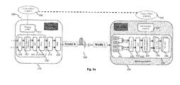
- Fig. 2a illustrates an example optical transmission system 200 comprising a transmitter 210, an optical transmission path 250 and a receiver 230.
- the optical transmission system 200 comprises a control plane 260 which may be used to manage the optical transmission system 200.
- the control plane 260 typically makes use of the network protocol suite GMPLS (Generalized Multi-Protocol Label Switching).
- GMPLS Generalized Multi-Protocol Label Switching
- the control plane 260 may be used to instruct the transmitter 210 and the receiver 230 to change the width of the WDM channel 111 used on the optical transmission path 250.
- the transmitter 210 comprises a first digital signal processor 218, which may e.g. be implemented as an ASIC (Application-specific integrated circuit).
- ASIC Application-specific integrated circuit
- the first digital signal processor 218 provides two sequences of symbols (e.g. QPSK symbols) 211 for the two polarizations of the optical signal, respectively.
- the two sequences of symbols 211 are filtered by a bank of two transmitter filters 212 for the two polarizations of the optical signal, respectively.
- the two transmitter filters 212 are identical, however, in other embodiments, the two transmitter filters 212 are specific for the respective polarizations of the optical signal.
- the transmitter 210 may comprise an LUT (Look-up Table) 213 for providing a list of pulse shaping filters.
- LUT Look-up Table
- a pair of Digital-to-Analogue-Converters (DAC) 214 is used to convert the filtered sequences of symbols 211 into a pair of electrical signals.
- the pair of electrical signals is used to modulate the two polarizations of the optical signal which is transmitted over the transmission path 250 (using drivers 215 and modulators 216, e.g. Mach-Zehnder-Modulators, MZM).
- the optical receiver 230 illustrated in Fig. 2a is a coherent optical receiver which is configured to convert the received optical signal into a pair of complex digital signals, wherein each digital signal comprises an in-phase component and a quadrature-phase component.
- the coherence receiver may comprise a coherent detector and a bank of Analogue-to-Digital Converters (ADC) 231.
- the optical receiver 230 comprises a second digital signal processor 238 (e.g. an ASIC) which processes the pair of digital signals, in order to recover the two sequences of symbols 211 in the decision units 236.
- the processing of the pair of digital signals typically comprises CD compensation 232, Clock Recovery (DCR) 233 and carrier frequency / carrier phase estimation 235.
- the processing typically comprises a polarization demultiplexing and equalization unit 234.
- the polarization demultiplexing unit 234 may comprise one or more equalization filters which are used for channel equalization and/or for polarization de-multiplexing.
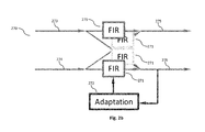
- the polarization demultiplexing unit 234 typically comprises a bank 270 of four FIR (Finite Impulse Response) filters 271 arranged in a butterfly structure (see Fig. 2b ).
- the filter taps of the FIR filters 271 may be determined and adapted continuously within a feedback loop comprising an adaptation unit 272.
- the adaptation unit 272 may execute a CMA algorithm which continuously adapts the filter taps in a "blind" manner.
- the CMA algorithm determines the filter taps of the FIR filters 271 solely based on the samples of the pair of digital signals derived from the received optical signal.
- the filter taps are typically determined such that the filtered signal downstream of the polarization de-multiplexing unit 234 (i.e. subsequent to filtering with the FIR filter bank 270) exhibits pre-determined signal characteristics.
- the CMA algorithm was introduced by Godard (IEEE Tr. Comm, vol.28, no.11. pp. 1867-1875, 1980 ) and the description thereof is incorporated by reference. Furthermore, the CMA is discussed in the document " Digital Equalization of 40Gbit/s per Wavelength Transmission over 2480km of Standard Fiber without Optical Dispersion Compensation", S.J. Savory et al., Proceedings of ECOC 2006, Paris, France, paper Th2.5.5, Sep. 2006 . The description of the CMA in this document is hereby incorporated by reference.
- the FIR filters 271 may typically be divided into two filter components, a so called common mode component and a so called differential mode component.
- the differential mode component is primarily responsible for turning the polarization plane of the received signal, in order to correctly identify the polarization planes of the two orthogonally polarized signal components.
- the common mode component is primarily responsible for removing undesirable cross-talk distortions within the received signal, which may be due to interferences of the particular WDM channel with neighboring WDM channels. As such, the common mode component is typically directed at isolating the signal portions of the particular WDM channel from signal portions originating from neighboring WDM channels.
- H 11 ( z ) and H 21 ( z ) be the FIR filters 271 which mix the pair of digital signals 273, 274 at the input of the polarization demultiplexing unit 234 to yield the first polarization demultiplexed digital signal 275 (at the output of the polarization demultiplexing unit 234).
- the common mode component of these two FIR filters may be determined as the square root of the sum of the squared absolute responses derived from the two FIR filters H 11 ( z ) and H 21 ( z ).
- the resulting filter may be referred to as the common mode FIR filter component for the first polarization or as the first common mode filter.
- the common mode FIR filter components for the second polarization may be determined from the filters H 12 ( z ) and H 22 ( z ) which mix the pair of digital signals 273, 274 at the input of the polarization demultiplexing unit 234 to yield the second polarization demultiplexed digital signal 276 (at the output of the polarization demultiplexing unit 234).
- the common mode components may be determined e.g. in the feedback unit 237.
- coherent receivers 230 typically use linear adaptive equalizers (which e.g. make use of CMA, decision directed LMS (Least Mean Square), ...) to demultiplex the received polarization tributaries after transmission.
- linear equalizers typically try to mitigate for inter-symbol interference induced penalties by enhancing highest frequencies of the spectrum. At low optical SNR, this may cause an enhancement of the noise contained in the signal bandwidth and thereby degrade the performance.
- the spectral response of the CMA may be analyzed in a low speed micro-controller in the feedback unit 237.
- the CMA algorithm typically operates at a lower update rate than the symbol rate (e.g. a factor 10 or 100 lower than the symbol rate). Consequently, the determination of the spectral response of the CMA, i.e. the determination of the FIR filters 271 may be performed at lower processor rates than the processing of the received digital signals.
- FIG. 3 An example of the impact of the tight filtering at the transmitter 210 onto the spectral response of the CMA filter (i.e. on the FIR filters 271) is shown in Fig. 3 .
- the spectral response 301 of the FIR filters 271 at the receiver 230 shows a clear enhancement of high frequencies. This enhancement of high frequencies can lead to a noise enhancement at low OSNR, thereby reducing the performance of the optical transmission system 200.
- the receiver 230 In order to reduce the effect of noise enhancement at the receiver 230, it is proposed to provide the spectral response 301 of the FIR filters 271 to the transmitter 210, and to thereby enable the transmitter 210 to design an appropriate transmitter filter 212 which reduces the undesirable enhancement of noise at the receiver 230. This can be done by making use of the control plane 260. In particular, the receiver 230 may pass information regarding the frequency response 301 of the FIR filters 271 to the control plane 260 and the control plane 260 may forward this information to the transmitter 210. Alternatively or in addition, a direct upstream communication process may be used as will be outlined at a later section of this document. Such a direct upstream communication process may be faster than a communication via the control plane 260, thereby increasing dynamics.
- the spectral response 301 of the FIR filters 271 may be approximated.
- the FIR filter response may be fitted, e.g. by a polynomial of a pre-determined degree or by a sinusoidal function.
- the receiver 230 and the transmitter 210 may make use of a common list of default spectral responses (also referred to as a bank of filtering functions).
- the receiver 230 (in particular the feedback unit 237) may be configured to select a default spectral response from the list which best approximates the actual spectral response 301 of the FIR filters 271. In this case, only the index from the list may be transmitted to the transmitter 230.
- the transmitter 230 is then configured (e.g. using the profiling unit 217) to recover the default spectral response from the common list using the transmitted index.
- the information regarding the spectral response 301 of the FIR filters 271 may be used by the transmitter 210 to modify the pulse shaping performed in the transmitter filter 212, and to thereby optimize (i.e. increase) the signal-to-noise ratio after polarization demultiplexing 234, and hence to optimize (i.e. increase) the performance of the optical transmission system 200.
- the FIR filters 271 of the polarization demultiplexing unit 234 typically comprise a common mode component.
- a specific common mode component may be determined for the first and second polarizations, respectively.
- the common mode component for the first polarization may be referred to as the first common mode component and the common mode component for the second polarization may be referred to as the second common mode component.
- the first common mode component may be derived from H 11 ( z ) and H 21 ( z ), and the second common mode component may be derived from H 12 ( z ) and H 22 ( z ).
- the frequency response 301 shown in Fig. 3 corresponds to the frequency response of the first or second common mode component.
- the receiver 230 e.g. the feedback unit 237) may be configured to provide information regarding the first and/or the second common mode component to the transmitter 210 (e.g. to the profiling unit 217 of the transmitter 210).
- Fig. 4 shows an example scheme 400 for adapting the transmitter filter 212 based on the FIR filters 271 using 32-Gbaud PDM-QPSK experimental data.
- the PDM-QPSK data 211 is filtered using a standard 33GHz channel filter having a frequency response 401.
- the polarization demultiplexing unit 234 e.g. using the CMA algorithm
- the spectral response 402 of the first or second common mode of the FIR filters 271 is shown in Fig. 4 .
- the spectral responses 402 of the first and second common mode components of the FIR filters 271 may be fitted to yield fitted spectral responses 403, which are fed back to the transmitter 210, thereby reducing the amount of data to be transmitted from the receiver 230 to the transmitter 210.
- the profiling unit 217 of the transmitter 210 may use the information received from the receiver 230 to adapt the spectral response of the transmitter filter 212, thereby increasing the SNR of the transmission channel.
- a pre-emphasis filter 404 may be applied to the sequences of symbols 211 prior to filtering using the standard transmitter filter 405 (which corresponds to the filter 401). That is, equivalently to modifying the pulse shape of the transmitter filter 212 in the time domain, the channel response may be modified at the transmitter side using the filtering profile received from the receiver 230.
- the spectral response 406 of the FIR filters 271 at the receiver 230 becomes more flat, thus reducing noise enhancement at low OSNR and improving the performance of the optical transmission system 200.
- a 0.5dB OSNR improvement due to filter optimization This improvement should be even larger for tighter filtering, i.e. for filtering at less than 33GHz, e.g. 25GHz.
- the receiver 230 and the transmitter 210 make use of an upstream or reverse communication path between a (far-end) transponder comprising the receiver 230 and a (near-end) transponder comprising the transmitter 210.
- the far-end transponder and the near-end transponder may make use of the communication protocols used for exchanging data (i.e. payload data) on the WDM channels 211, 212 of the optical communication system 200.
- the far-end transponder 230 and the near-end transponder 210 may make use of the Optical Transport Network (OTN) protocol framework specified in ITU-T standard G.709.
- OTN Optical Transport Network
- the OTN framework defines how to route payload data across an optical communication system 200.
- the payload data is embedded into so called frames, wherein each frame comprises a frame overhead.
- the frame overhead comprises a plurality of fields (bytes), wherein the plurality of fields may be used to implement specific communication and control channels between the network elements (e.g. the far-end transponder comprising the receiver 230 and the near-end transponder comprising the transmitter 210) of the optical communication system 200.
- the overhead of the OTN frames (typically referred to as Optical Transport Unit (OTUk) frames) are directly accessible by the near-end transponder and the far-end transponder.
- OFT Optical Transport Unit
- the far-end transponder (comprising the receiver 230) may insert the information regarding the filter response of the FIR filters 271 into a pre-determined byte of the overhead of an OTUk frame which is sent via an optical communication channel from the far-end transponder to the near-end transponder (comprising the transmitter 210), thereby informing the near-end transponder on how to adapt the profile of the transmitter filter 212.
- the feedback communication link can be implemented as an in-band communication link between the far-end transponder (comprising the receiver 230) and the near-end transponder (comprising the transmitter 210).
- a scheme for determining transmitter filters for a tightly spaced WDM transmission system has been described.
- the scheme allows the determination of the transmitter filter for a particular WDM transmission channel based on the frequency response of equalizer filters at the receiver of the WDM transmission channel.
- the performance of the WDM transmission channel can be improved.
- the proposed scheme enables the optimization of the signal-to-noise ratio in coherent receivers in the context of ultra dense WDM systems.
- the proposed scheme enables the flexible optimization of the performance of tightly filtered signals in ultra dense WDM systems, which translates into longer maximum transmission distances.
- the proposed scheme may be performed during the ramp up phase of a WDM transmission channel (e.g. subsequent to a modification of the width of the WDM channel or subsequent to an initial set up of the WDM channel). Furthermore, the proposed scheme may be performed regularly, in order to adapt the pulse shaping at the transmitter to changing channel conditions. As indicated above, the adaptation of the transmitter filter may be performed for each polarization of the PDM signal separately. Alternatively, a common transmitter filter may be used for both polarizations. In the latter case, information regarding a common mode of all of the FIR filters may be fed back from the receiver to the transmitter. The common mode of all of the FIR filters may be derived as the sum of and/or as the average of all of the FIR filters.
- steps of various above-described methods and components of described systems can be performed by programmed computers.
- program storage devices e.g., digital data storage media, which are machine or computer readable and encode machine-executable or computer-executable programs of instructions, wherein said instructions perform some or all of the steps of said above-described methods.
- the program storage devices may be, e.g., digital memories, magnetic storage media such as a magnetic disks and magnetic tapes, hard drives, or optically readable digital data storage media.
- the embodiments are also intended to cover computers programmed to perform said steps of the above-described methods.
- processor or “controller” should not be construed to refer exclusively to hardware capable of executing software, and may implicitly include, without limitation, digital signal processor (DSP) hardware, network processor, application specific integrated circuit (ASIC), field programmable gate array (FPGA), read only memory (ROM) for storing software, random access memory (RAM), and non volatile storage.
- DSP digital signal processor
- ASIC application specific integrated circuit
- FPGA field programmable gate array
- ROM read only memory
- RAM random access memory
- non volatile storage Other hardware, conventional and/or custom, may also be included.
- any block diagrams herein represent conceptual views of illustrative circuitry embodying the principles of the invention.
- any flow charts, flow diagrams, state transition diagrams, pseudo code, and the like represent various processes which may be substantially represented in computer readable medium and so executed by a computer or processor, whether or not such computer or processor is explicitly shown.
Abstract
Description
- The present document relates to optical communication systems. In particular, the present document relates to high efficiency wavelength division multiplexing (WDM) optical communication systems.
- High spectral efficiency optical communication systems are interesting in order to cope with the foreseen demand for capacity increase in optical communication networks. In this context, multi-level modulation formats (e.g. quadrature phase shift keying, QPSK) combined with polarization multiplexing (PDM), as well as digital coherent detection techniques are being investigated. Polarization division multiplexed quadrature phase shift keying (PDM-QPSK) paired with coherent detection may be used to achieve a transmission rate of 112 Gb/s (typically referred to as 100Gb/s). This format yields a spectral efficiency of 2b/s/Hz in a standard WDM transmission system based on a 50GHz grid between two adjacent WDM channels (as shown in the WDM channel diagram 100 of
Fig. 1 , where allWDM channels 101 have the same channel width). One possible approach to increase the spectral efficiency of such 100Gb/s systems is to use higher level modulation formats like PDM-8QAM, PDM-16QAM, etc. However, such formats typically have a lower sensitivity to optical noise and a weaker tolerance to nonlinear effects, and therefore may result in a reduction of the transmission reach compared to PDM-QPSK. - Another approach to further increase the spectral efficiency of 100Gb/s optical transmission systems is to tightly pack WDM channels, i.e. to reduce the channel spacing between adjacent WDM channels. Transmission with 3b/s/Hz or 4b/s/Hz spectral efficiency may be achieved using 100Gb/s PDM-QPSK channels over a 33GHz and a 25GHz grid, respectively (instead of a conventional 50GHz grid).
- Flexible grid WDM systems may be used in order to optimize bandwidth occupancy depending on an (optimum) trade-off between transmitted capacity and transmission reach. By way of example, a semi-flexible system architecture may be used having a granularity of 12.5GHz (starting from the ITU grid) in order to define channel slots of different width, instead of having a fixed 50GHz grid. This enables to vary the channel packing in a pre-determined range depending on the (optimum) trade-off between optical path impairments and required capacity. This is shown in the WDM channel diagram 110 of
Fig. 1 , wheredifferent WDM channels 111, 123 have different channel widths. - WDM systems working with reduced channel spacing appear to be an efficient method to increase system capacity with only a limited reduction of the transmission reach. However, the optimization of the signal-to-noise-ratio (SNR) at the optical receiver of a transmission channel is challenging in flexible grid systems as the different filtering functions used for the
WDM channels - According to an aspect an optical transmitter is described. The optical transmitter is adapted to transmit an optical signal on an optical wavelength division multiplexed (WDM) transmission channel to a corresponding optical receiver. The WDM transmission channel may have a pre-determined bandwidth which may depend on a pre-determined grid of WDM channels. The bandwidth may be adjustable in accordance to the grid of WDM channels. By way of example, the bandwidth may be adjustable on a grid granularity of 12.5GHz. The optical transmitter may be adapted to adjust to the bandwidth of the WDM transmission channel.
- The optical transmitter comprises a profiling unit adapted to receive information regarding an equalization filter, wherein the equalization filter has been adapted or adjusted at the corresponding optical receiver. The equalization filter may be used by the corresponding optical receiver to compensate for distortions incurred by a first optical signal transmitted from the optical transmitter over the WDM transmission channel to the optical receiver. The first optical signal is typically representative of a first sequence of data symbols. In particular, the first optical signal may have been obtained by modulating an optical carrier signals with a sequence of symbols derived from the first sequence of data symbols. In this context, the equalization filter may be used by the corresponding optical receiver to compensate for pulse shaping filtering performed at the optical transmitter. Such pulse shaping filtering may be performed at the optical transmitter in order to adjust the first sequence of data symbols and consequently the first optical signal to the bandwidth of the WDM transmission channel. As such, the equalization filter may have been adapted at the corresponding optical receiver based on the first optical signal received from the optical transmitter.
- Furthermore, the optical transmitter comprises a pulse shaping filter unit adapted to filter a second sequence of data symbols using a pulse shaping filter, thereby yielding a filtered sequence of data symbols. A frequency response of the pulse shaping filter may depend on the information regarding the equalization filter. In other words, the pulse shaping filter may be adjusted in accordance to the information regarding the equalization filter received from the optical receiver.
- In addition, the optical transmitter may comprise a digital-to-optical converter adapted to convert the filtered sequence of data symbols into a second optical signal to be transmitted to the optical receiver over the WDM transmission channel. The digital-to-optical converter may comprise one or more digital-to-analogue converters (DACs) and a modulation unit for modulating an optical carrier signal with the filtered sequence of symbols to yield the second optical signal.
- As such, the optical transmitter may be configured to adapt its pulse shaping filter based on information received from the corresponding optical receiver and to thereby increase a signal-to-noise ratio (SNR) of the signals received at the optical receiver. This process may be performed during a ramp-up phase of the optical transmitter and the optical receiver (e.g. subsequent to a change of the bandwidth of the WDM transmission channel). By way of example, the optical transmitter may be adapted to use a default transmitter filter (as the pulse shaping filter) when filtering the first sequence of data symbols for the first optical signal. The optical receiver may then adapt the equalization filter based on the received first optical signal and provide the optical transmitter with information regarding the equalization filter. The optical transmitter may then adjust the pulse shaping filter based on the information regarding the equalization filter and generate the second optical signal (subsequent to the first optical signal) using the adjusted pulse shaping filter (and not the default transmitter filter). As a result, the optical transmitter and the optical receiver may be adapted to the (changed) bandwidth of the WDM transmission channel.
- The pulse shaping filter may correspond to a pre-emphasis filter depending on the information regarding the equalization filter. As such, the pulse shaping filter unit may be adapted to filter the second sequence of data symbols using the pre-emphasis filter. Furthermore, the pulse shaping filter unit may be adapted to further filter the filtered sequence of data symbols using the default transmitter filter, wherein the default transmitter filter is typically adapted to the bandwidth of the WDM transmission channel. Alternatively, the pulse shaping filter may correspond to a combination of a pre-emphasis filter which depends on the information regarding the equalization filter, and of the default transmitter filter which is typically adapted to the bandwidth of the WDM transmission channel. In the latter case, the pulse shaping filter unit may be adapted to apply a single combined pulse shaping filter (instead of applying the pre-emphasis filter and the default transmitter filter sequentially).
- The profiling unit may be adapted to determine the pre-emphasis filter such that a frequency response of the pre-emphasis filter approximates a filter response of the equalization filter. For this purpose, the profiling unit may make use of the information regarding the equalization filter. By way of example, the information regarding the equalization filter may comprise one or more of the following: one or more fitting parameters of a fitting curve approximating the frequency response of the equalization filter, one or more filter coefficients of the equalization filter and/or an index to a pre-determined list of filters identifying a filter selected at the corresponding receiver, wherein a frequency response of the selected filter approximates the frequency response of the equalization filter.
- According to a further aspect, an optical receiver adapted to receive an optical signal on an optical wavelength division multiplexed (WDM) transmission channel from a corresponding transmitter is described. The optical receiver comprises an optical-to-digital converter adapted to convert the first optical signal received from the optical transmitter into a digital signal. The optical receiver may be a coherent optical receiver. As such, the optical-to-digital converter may comprise a coherent optical detection unit providing one or more pairs of analog electrical signals, wherein a pair of analog electrical signals comprises an in-phase and a quadrature-phase signal (also referred to as components). Furthermore, the optical-to-digital converter may comprise one or more analogue-to-digital converters (ADCs), converting the analogs signals to the digital signal. The digital signal is representative of the first sequence of data symbols which was used at the optical transmitter for modulating the first optical signal.
- The optical receiver comprises an equalization unit adapted to filter the digital signal using an equalization filter, thereby yielding a filtered digital signal. Furthermore, the optical receiver comprises an adaptation unit configured to adapt the equalization filter in order to compensate for a transfer function of the WDM transmission channel and in order to compensate for a pulse shaping filter (e.g. the default transmitter filter) applied to the first sequence of data symbols at the corresponding transmitter. The adaptation unit may be configured to determine the equalization filter based on the digital signal (which is derived from the first optical signal). By way of example, the adaptation unit may make use of blind adaptation techniques such as the Constant Modulus Algorithm to determine the equalization filter. Alternatively or in addition, the adaptation unit may make use of training based adaptation techniques. By way of example, the first optical signal may comprise a sequence of training symbols known to the optical receiver, thereby enabling the optical receiver to better adapt the equalization filter to the transfer function of the WDM transmission channel and/or to the pulse shaping filter of the optical transmitter.
- The optical receiver further comprises a feedback unit adapted to provide information regarding the equalization filter to the corresponding transmitter for the purpose of modification of the pulse shaping filter. The feedback unit may make use of a control plane or of another WDM transmission channel to transmit this information regarding the equalization filter to the optical transmitter.
- Furthermore, the optical receiver may comprise a decision unit adapted to estimate the first sequence of data symbols based on the filtered digital signal.
- The optical receiver and the optical transmitter may be adapted for the transmission of polarization division multiplexed (PDM) optical signals. As such, the first optical signal (and the second optical signal) may be polarization division multiplexed optical signal comprising a first and a second polarization, respectively, and the digital signal may comprise a first polarization component (or a digital signal for the first polarization) and a second polarization component (or a digital signal for the second polarization). In a similar manner, the filtered digital signal may comprise a first polarization component and a second polarization component. In case of a coherent optical receiver, each of the polarization components may comprise an in-phase component and a quadrature-phase component, respectively.
- In case of PDM, the equalization unit may be a polarization de-multiplexing unit and the equalization filter may comprise a plurality of Finite Impulse Response, referred to as FIR, filters in a butterfly structure. The feedback unit may be adapted to determine the information regarding the equalization filter based on the plurality of FIR filters. In particular, the feedback unit may be adapted to determine a common mode component of the plurality of FIR filters for the first and second polarizations, respectively. The common mode component for the first (second) polarization may e.g. be determined based on the sum of the FIR filters of the equalization filter which contribute to the first (second) polarization of the filtered digital signal. In particular, the common mode component for the first (second) polarization may e.g. be determined based on the sum of the squared absolute responses derived from the FIR filters of the equalization filter which contribute to the first (second) polarization of the filtered digital signal. Hence, the information regarding the equalization filter may be determined based on the common mode component for the first and/or second polarizations.
- As indicated above, the information regarding the equalization filter may comprise filter coefficients of a filter derived from the equalization filter. Alternatively or in addition, the feedback unit may be adapted to approximate a frequency response of the equalization filter, e.g. using a pre-determined fitting curve such as a polynomial of a certain order or a sinusoidal fitting curve, thereby approximating the frequency response using one or more fitting parameters. The fitting may be performed by reducing / minimizing e.g. a mean square error. The feedback unit may be adapted to determine the information regarding the equalization filter based on the approximated frequency response of the equalization filter. The information regarding the equalization filter may comprise the one or more fitting parameters. Alternatively or in addition, the feedback unit may be adapted to approximate the equalization filter by selecting a filter from a pre-determined list of filters. The frequency response of the selected filter may approximate the frequency response of the equalization filter (e.g. by reducing / minimizing a mean square error). In such cases, the information regarding the equalization filter may comprise an index to the pre-determined list of filters possibly stored in a look-up table (LUT) identifying the selected filter.
- According to a further aspect, an optical transmission system adapted for wavelength division multiplexed (WDM) transmission is described. The optical transmission system comprises an optical transmitter according to any of the aspects outlined in the present document. Furthermore, the optical transmission system comprises an optical receiver according any of the aspects outlined in the present document. In addition, the optical transmission system may comprise a feedback path adapted to carry the information regarding the equalization filter from the optical receiver to the optical transmitter. The feedback path may comprise one or more of the following: a control plane of the optical transmission system or a WDM transmission channel from a far-end transponder comprising the optical receiver to a near-end transponder comprising the optical transmitter.
- According to another aspect, a method for increasing a signal-to-noise ratio and the overall performance of an optical transmission system comprising an optical transmitter and a corresponding optical receiver is described. The method comprises receiving information regarding an equalization filter, wherein the equalization filter has been adapted at the optical receiver. The method proceeds in filtering a sequence of data symbols using a pulse shaping filter, thereby yielding a filtered sequence of data symbols. The frequency response of the pulse shaping filter depends on the information regarding the equalization filter. Furthermore, the method may comprise converting the filtered sequence of data symbols into an optical signal and/or transmitting the optical signal to the optical receiver.
- According to a further aspect, a software program is described. The software program may be adapted for execution on a processor and for performing the method steps outlined in the present document when carried out on a computing device.
- According to another aspect, a storage medium is described. The storage medium may comprise a software program adapted for execution on a processor and for performing the method steps outlined in the present document when carried out on a computing device.
- According to a further aspect, a computer program product is described. The computer program may comprise executable instructions for performing the method steps outlined in the present document when executed on a computer.
- It should be noted that the methods and systems including its preferred embodiments as outlined in the present patent application may be used stand- alone or in combination with the other methods and systems disclosed in this document. Furthermore, all aspects of the methods and systems outlined in the present patent application may be arbitrarily combined. In particular, the features of the claims may be combined with one another in an arbitrary manner.
- The invention is explained below in an exemplary manner with reference to the accompanying drawings, wherein
-
Fig. 1 illustrates example WDM channels on a fixed and on a flexible frequency grid; -
Fig. 2a shows a block diagram of an example optical transmission system; -
Fig. 2b shows the block diagram of an example filter bank used in a polarization demultiplexer unit; -
Fig. 3 illustrates the frequency response of example optical filters at the transmitter and the receiver of an optical transmission system; and -
Fig. 4 illustrates an example method for adapting the optical filter at the transmitter based on one or more filters determined at the receiver of an optical transmission system. - As outlined in the introductory section, WDM channels of different widths may be used to adapt the capacity of an optical transmission system to impairments on the optical transmission paths.
WDM channels Fig. 1 . When adapting the width of aWDM channel 111, the transmitter filter used at the transmitter of theWDM channel 111 typically has to be adapted to the reduced or increase bandwidth of theWDM channel 111. Such a transmitter filter is mainly used for pulse shaping, in order to reduce the crosstalk betweenadjacent WDM channels WDM channel 111, the transmitter filter may be provided with a variable attenuation profile, thereby enabling to adjust the cut-off frequency of the transmitter filter to the modified width of theWDM channel 111. In the present document, it is proposed to dynamically determine the filtering profile used at the transmitter side such that the received SNR at the receiver side is optimized (i.e. increased). Hence, it is proposed to determine a transmitter filter which optimizes the performance of the overall optical transmission channel. It is proposed to optimize the filtering profile at the transmitter side by analyzing the response of one or more of the (linear) adaptive equalizers used in the (coherent) receiver. The adaptive one or more equalizers at the receiver may make use of a constant modulus algorithm, CMA or other blind adaptation techniques. In other words, it is proposed to determine the transmitter filter at the transmitter based on information regarding the transfer function of the optical transmission channel which is available at the corresponding receiver. As such, it is possible to modify the width of aWDM channel 111 and to automatically adapt the transmitter filter at the transmitter to the modifiedWDM channel 111, wherein the automatically adapted transmitter filter optimizes (i.e. increases) the SNR at the receiver. -
Fig. 2a illustrates an exampleoptical transmission system 200 comprising atransmitter 210, anoptical transmission path 250 and areceiver 230. Furthermore, theoptical transmission system 200 comprises acontrol plane 260 which may be used to manage theoptical transmission system 200. Thecontrol plane 260 typically makes use of the network protocol suite GMPLS (Generalized Multi-Protocol Label Switching). By way of example, thecontrol plane 260 may be used to instruct thetransmitter 210 and thereceiver 230 to change the width of theWDM channel 111 used on theoptical transmission path 250. - The
transmitter 210 comprises a firstdigital signal processor 218, which may e.g. be implemented as an ASIC (Application-specific integrated circuit). In the illustrated example atransmitter 210 for polarization multiplexed optical signals is depicted. The firstdigital signal processor 218 provides two sequences of symbols (e.g. QPSK symbols) 211 for the two polarizations of the optical signal, respectively. The two sequences ofsymbols 211 are filtered by a bank of twotransmitter filters 212 for the two polarizations of the optical signal, respectively. In an embodiment, the twotransmitter filters 212 are identical, however, in other embodiments, the twotransmitter filters 212 are specific for the respective polarizations of the optical signal. In addition, thetransmitter 210 may comprise an LUT (Look-up Table) 213 for providing a list of pulse shaping filters. A pair of Digital-to-Analogue-Converters (DAC) 214 is used to convert the filtered sequences ofsymbols 211 into a pair of electrical signals. The pair of electrical signals is used to modulate the two polarizations of the optical signal which is transmitted over the transmission path 250 (usingdrivers 215 andmodulators 216, e.g. Mach-Zehnder-Modulators, MZM). - The
optical receiver 230 illustrated inFig. 2a is a coherent optical receiver which is configured to convert the received optical signal into a pair of complex digital signals, wherein each digital signal comprises an in-phase component and a quadrature-phase component. For this purpose, the coherence receiver may comprise a coherent detector and a bank of Analogue-to-Digital Converters (ADC) 231. Furthermore, theoptical receiver 230 comprises a second digital signal processor 238 (e.g. an ASIC) which processes the pair of digital signals, in order to recover the two sequences ofsymbols 211 in thedecision units 236. The processing of the pair of digital signals typically comprisesCD compensation 232, Clock Recovery (DCR) 233 and carrier frequency /carrier phase estimation 235. - Furthermore, the processing typically comprises a polarization demultiplexing and
equalization unit 234. Thepolarization demultiplexing unit 234 may comprise one or more equalization filters which are used for channel equalization and/or for polarization de-multiplexing. Thepolarization demultiplexing unit 234 typically comprises abank 270 of four FIR (Finite Impulse Response) filters 271 arranged in a butterfly structure (seeFig. 2b ). The filter taps of the FIR filters 271 may be determined and adapted continuously within a feedback loop comprising anadaptation unit 272. Theadaptation unit 272 may execute a CMA algorithm which continuously adapts the filter taps in a "blind" manner. In other words, the CMA algorithm determines the filter taps of the FIR filters 271 solely based on the samples of the pair of digital signals derived from the received optical signal. The filter taps are typically determined such that the filtered signal downstream of the polarization de-multiplexing unit 234 (i.e. subsequent to filtering with the FIR filter bank 270) exhibits pre-determined signal characteristics. By way of example, for signals of unit amplitude, the CMA may try to minimize the magnitude of the error term E = (|sout |-1)2 at the output of thepolarization de-multiplexing unit 234, wherein |sout | is the intensity (or amplitude) of an output signal sout of thepolarization de-multiplexing unit 234. - The CMA algorithm was introduced by Godard (IEEE Tr. Comm, vol.28, no.11. pp. 1867-1875, 1980) and the description thereof is incorporated by reference. Furthermore, the CMA is discussed in the document "Digital Equalization of 40Gbit/s per Wavelength Transmission over 2480km of Standard Fiber without Optical Dispersion Compensation", S.J. Savory et al., Proceedings of ECOC 2006, Cannes, France, paper Th2.5.5, Sep. 2006. The description of the CMA in this document is hereby incorporated by reference.
- The FIR filters 271 of the
polarization demultiplexing unit 234 may be denoted as
FIR filters 271 and with cij,n,n=0,...,N-1 being the N filter taps of the respective FIR filters 271, N being in the range of 10. The FIR filters 271 may typically be divided into two filter components, a so called common mode component and a so called differential mode component. The differential mode component is primarily responsible for turning the polarization plane of the received signal, in order to correctly identify the polarization planes of the two orthogonally polarized signal components. The common mode component is primarily responsible for removing undesirable cross-talk distortions within the received signal, which may be due to interferences of the particular WDM channel with neighboring WDM channels. As such, the common mode component is typically directed at isolating the signal portions of the particular WDM channel from signal portions originating from neighboring WDM channels. - Let H 11(z) and H 21(z) be the FIR filters 271 which mix the pair of
digital signals polarization demultiplexing unit 234 to yield the first polarization demultiplexed digital signal 275 (at the output of the polarization demultiplexing unit 234). The common mode component of these two FIR filters may be determined as the square root of the sum of the squared absolute responses derived from the two FIR filters H 11(z) and H 21(z). The resulting filter may be referred to as the common mode FIR filter component for the first polarization or as the first common mode filter. In a similar manner, the common mode FIR filter components for the second polarization (or the second common mode filter) may be determined from the filters H 12(z) and H 22(z) which mix the pair ofdigital signals polarization demultiplexing unit 234 to yield the second polarization demultiplexed digital signal 276 (at the output of the polarization demultiplexing unit 234). The common mode components may be determined e.g. in thefeedback unit 237. - As such,
coherent receivers 230 typically use linear adaptive equalizers (which e.g. make use of CMA, decision directed LMS (Least Mean Square), ...) to demultiplex the received polarization tributaries after transmission. These linear equalizers typically try to mitigate for inter-symbol interference induced penalties by enhancing highest frequencies of the spectrum. At low optical SNR, this may cause an enhancement of the noise contained in the signal bandwidth and thereby degrade the performance. In order to avoid this issue, it is proposed to use the spectral profile of the linear equalizer response at thereceiver 230 to adapt the filtering profile used by thetransmitter filter 212 at thetransmitter 210 and thereby maximize (i.e. increase) the energy of the transmitted signal with respect to the received bandwidth. For this purpose, the spectral response of the CMA may be analyzed in a low speed micro-controller in thefeedback unit 237. In other words, the CMA algorithm typically operates at a lower update rate than the symbol rate (e.g. afactor 10 or 100 lower than the symbol rate). Consequently, the determination of the spectral response of the CMA, i.e. the determination of the FIR filters 271 may be performed at lower processor rates than the processing of the received digital signals. - An example of the impact of the tight filtering at the
transmitter 210 onto the spectral response of the CMA filter (i.e. on the FIR filters 271) is shown inFig. 3 . After filtering experimentally a 32-Gbaud PDM-QPSK signal with a 33-GHz bandwidth interleaver (i.e. with atransmitter filter 212 having afrequency response 300 illustrated inFig. 3 ), thespectral response 301 of the FIR filters 271 at thereceiver 230 shows a clear enhancement of high frequencies. This enhancement of high frequencies can lead to a noise enhancement at low OSNR, thereby reducing the performance of theoptical transmission system 200. - In order to reduce the effect of noise enhancement at the
receiver 230, it is proposed to provide thespectral response 301 of the FIR filters 271 to thetransmitter 210, and to thereby enable thetransmitter 210 to design anappropriate transmitter filter 212 which reduces the undesirable enhancement of noise at thereceiver 230. This can be done by making use of thecontrol plane 260. In particular, thereceiver 230 may pass information regarding thefrequency response 301 of the FIR filters 271 to thecontrol plane 260 and thecontrol plane 260 may forward this information to thetransmitter 210. Alternatively or in addition, a direct upstream communication process may be used as will be outlined at a later section of this document. Such a direct upstream communication process may be faster than a communication via thecontrol plane 260, thereby increasing dynamics. - It should be noted that in order to reduce the amount of information that is transmitted from the
receiver 230 to thetransmitter 210, thespectral response 301 of the FIR filters 271 may be approximated. For this purpose, the FIR filter response may be fitted, e.g. by a polynomial of a pre-determined degree or by a sinusoidal function. As a result, only the reduced number of fitting parameters is transmitted from thereceiver 230 to thetransmitter 210. Alternatively or in addition, thereceiver 230 and thetransmitter 210 may make use of a common list of default spectral responses (also referred to as a bank of filtering functions). The receiver 230 (in particular the feedback unit 237) may be configured to select a default spectral response from the list which best approximates the actualspectral response 301 of the FIR filters 271. In this case, only the index from the list may be transmitted to thetransmitter 230. Thetransmitter 230 is then configured (e.g. using the profiling unit 217) to recover the default spectral response from the common list using the transmitted index. - The information regarding the
spectral response 301 of the FIR filters 271 (e.g. the FIR filter coefficients, the fitting parameters and/or an index to a common list of default filters) may be used by thetransmitter 210 to modify the pulse shaping performed in thetransmitter filter 212, and to thereby optimize (i.e. increase) the signal-to-noise ratio afterpolarization demultiplexing 234, and hence to optimize (i.e. increase) the performance of theoptical transmission system 200. - As outlined above, the FIR filters 271 of the
polarization demultiplexing unit 234 typically comprise a common mode component. In particular, a specific common mode component may be determined for the first and second polarizations, respectively. The common mode component for the first polarization may be referred to as the first common mode component and the common mode component for the second polarization may be referred to as the second common mode component. The first common mode component may be derived from H 11(z) and H 21(z), and the second common mode component may be derived from H 12(z) and H 22(z). Thefrequency response 301 shown inFig. 3 corresponds to the frequency response of the first or second common mode component. As such, the receiver 230 (e.g. the feedback unit 237) may be configured to provide information regarding the first and/or the second common mode component to the transmitter 210 (e.g. to theprofiling unit 217 of the transmitter 210). -
Fig. 4 shows anexample scheme 400 for adapting thetransmitter filter 212 based on the FIR filters 271 using 32-Gbaud PDM-QPSK experimental data. The PDM-QPSK data 211 is filtered using a standard 33GHz channel filter having afrequency response 401. At thereceiver 230, the polarization demultiplexing unit 234 (e.g. using the CMA algorithm) yields abank 270 of FIR filters 271. Thespectral response 402 of the first or second common mode of the FIR filters 271 is shown inFig. 4 . Thespectral responses 402 of the first and second common mode components of the FIR filters 271 may be fitted to yield fittedspectral responses 403, which are fed back to thetransmitter 210, thereby reducing the amount of data to be transmitted from thereceiver 230 to thetransmitter 210. - The
profiling unit 217 of thetransmitter 210 may use the information received from thereceiver 230 to adapt the spectral response of thetransmitter filter 212, thereby increasing the SNR of the transmission channel. Alternatively, apre-emphasis filter 404 may be applied to the sequences ofsymbols 211 prior to filtering using the standard transmitter filter 405 (which corresponds to the filter 401). That is, equivalently to modifying the pulse shape of thetransmitter filter 212 in the time domain, the channel response may be modified at the transmitter side using the filtering profile received from thereceiver 230. - After this modification of the filtering performed at the
transmitter 210, thespectral response 406 of the FIR filters 271 at thereceiver 230 becomes more flat, thus reducing noise enhancement at low OSNR and improving the performance of theoptical transmission system 200. Experiments have shown e.g. a 0.5dB OSNR improvement due to filter optimization. This improvement should be even larger for tighter filtering, i.e. for filtering at less than 33GHz, e.g. 25GHz. - In the following, a possible implementation of a direct feedback link between the
receiver 230 and thetransmitter 210 is described, in order to provide the feedback information regarding the FIR filters 271 to thetransmitter 210. For this purpose, thereceiver 230 and thetransmitter 210 make use of an upstream or reverse communication path between a (far-end) transponder comprising thereceiver 230 and a (near-end) transponder comprising thetransmitter 210. The far-end transponder and the near-end transponder may make use of the communication protocols used for exchanging data (i.e. payload data) on theWDM channels optical communication system 200. In particular, the far-end transponder 230 and the near-end transponder 210 may make use of the Optical Transport Network (OTN) protocol framework specified in ITU-T standard G.709. The OTN framework defines how to route payload data across anoptical communication system 200. The payload data is embedded into so called frames, wherein each frame comprises a frame overhead. The frame overhead comprises a plurality of fields (bytes), wherein the plurality of fields may be used to implement specific communication and control channels between the network elements (e.g. the far-end transponder comprising thereceiver 230 and the near-end transponder comprising the transmitter 210) of theoptical communication system 200. The overhead of the OTN frames (typically referred to as Optical Transport Unit (OTUk) frames) are directly accessible by the near-end transponder and the far-end transponder. - Consequently, the far-end transponder (comprising the receiver 230) may insert the information regarding the filter response of the FIR filters 271 into a pre-determined byte of the overhead of an OTUk frame which is sent via an optical communication channel from the far-end transponder to the near-end transponder (comprising the transmitter 210), thereby informing the near-end transponder on how to adapt the profile of the
transmitter filter 212. As such, the feedback communication link can be implemented as an in-band communication link between the far-end transponder (comprising the receiver 230) and the near-end transponder (comprising the transmitter 210). - In the present document, a scheme for determining transmitter filters for a tightly spaced WDM transmission system has been described. The scheme allows the determination of the transmitter filter for a particular WDM transmission channel based on the frequency response of equalizer filters at the receiver of the WDM transmission channel. As a result, the performance of the WDM transmission channel can be improved. In particular, the proposed scheme enables the optimization of the signal-to-noise ratio in coherent receivers in the context of ultra dense WDM systems. Moreover, the proposed scheme enables the flexible optimization of the performance of tightly filtered signals in ultra dense WDM systems, which translates into longer maximum transmission distances.
- The proposed scheme may be performed during the ramp up phase of a WDM transmission channel (e.g. subsequent to a modification of the width of the WDM channel or subsequent to an initial set up of the WDM channel). Furthermore, the proposed scheme may be performed regularly, in order to adapt the pulse shaping at the transmitter to changing channel conditions. As indicated above, the adaptation of the transmitter filter may be performed for each polarization of the PDM signal separately. Alternatively, a common transmitter filter may be used for both polarizations. In the latter case, information regarding a common mode of all of the FIR filters may be fed back from the receiver to the transmitter. The common mode of all of the FIR filters may be derived as the sum of and/or as the average of all of the FIR filters.
- It should be noted that the description and drawings merely illustrate the principles of the proposed methods and systems. It will thus be appreciated that those skilled in the art will be able to devise various arrangements that, although not explicitly described or shown herein, embody the principles of the invention and are included within its spirit and scope. Furthermore, all examples recited herein are principally intended expressly to be only for pedagogical purposes to aid the reader in understanding the principles of the proposed methods and systems and the concepts contributed by the inventors to furthering the art, and are to be construed as being without limitation to such specifically recited examples and conditions. Moreover, all statements herein reciting principles, aspects, and embodiments of the invention, as well as specific examples thereof, are intended to encompass equivalents thereof.
- Furthermore, it should be noted that steps of various above-described methods and components of described systems can be performed by programmed computers. Herein, some embodiments are also intended to cover program storage devices, e.g., digital data storage media, which are machine or computer readable and encode machine-executable or computer-executable programs of instructions, wherein said instructions perform some or all of the steps of said above-described methods. The program storage devices may be, e.g., digital memories, magnetic storage media such as a magnetic disks and magnetic tapes, hard drives, or optically readable digital data storage media. The embodiments are also intended to cover computers programmed to perform said steps of the above-described methods.
- In addition, it should be noted that the functions of the various elements described in the present patent document may be provided through the use of dedicated hardware as well as hardware capable of executing software in association with appropriate software. When provided by a processor, the functions may be provided by a single dedicated processor, by a single shared processor, or by a plurality of individual processors, some of which may be shared. Moreover, explicit use of the term "processor" or "controller" should not be construed to refer exclusively to hardware capable of executing software, and may implicitly include, without limitation, digital signal processor (DSP) hardware, network processor, application specific integrated circuit (ASIC), field programmable gate array (FPGA), read only memory (ROM) for storing software, random access memory (RAM), and non volatile storage. Other hardware, conventional and/or custom, may also be included.
- Finally, it should be noted that any block diagrams herein represent conceptual views of illustrative circuitry embodying the principles of the invention. Similarly, it will be appreciated that any flow charts, flow diagrams, state transition diagrams, pseudo code, and the like represent various processes which may be substantially represented in computer readable medium and so executed by a computer or processor, whether or not such computer or processor is explicitly shown.
Claims (15)
- An optical transmitter (210) adapted to transmit an optical signal on an optical wavelength division multiplexed, referred to as WDM, transmission channel (111) to a corresponding optical receiver (230), the optical transmitter (210) comprising- a profiling unit (217) adapted to receive information regarding an equalization filter (270) adapted at the corresponding optical receiver (230), based on a first optical signal received from the optical transmitter (210);- a pulse shaping filter unit (212) adapted to filter a second sequence of data symbols (211) using a pulse shaping filter, thereby yielding a filtered sequence of data symbols (211); wherein a frequency response (404, 405) of the pulse shaping filter depends on the information regarding the equalization filter (270); and- a digital-to-optical converter (214, 215 216) adapted to convert the filtered sequence of data symbols (211) into a second optical signal to be transmitted to the optical receiver (230).
- The optical transmitter (210) of claim 1, wherein- the pulse shaping filter is a pre-emphasis filter depending on the information regarding the equalization filter (270); and- the pulse shaping filter unit (212) is adapted to further filter the filtered sequence of data symbols (211) using a default transmitter filter adapted to a bandwidth of the WDM transmission channel (111).
- The optical transmitter (210) of claim 1, wherein the pulse shaping filter corresponds to a combination of a pre-emphasis filter depending on the information regarding the equalization filter (270) and a default transmitter filter adapted to a bandwidth of the WDM transmission channel (111).
- The optical transmitter (210) of any of claims 2 to 3, wherein the profiling unit (217) is adapted to- determine the pre-emphasis filter having a frequency response which approximates a filter response of the equalization filter (270), based on the information regarding the equalization filter (270).
- The optical transmitter (210) of any previous claim, wherein the information regarding the equalization filter (270) comprises one or more of- one or more fitting parameters of a fitting curve approximating a frequency response of the equalization filter (270);- one or more filter coefficients of the equalization filter (270); and- an index to a pre-determined list of filters identifying a filter selected at the corresponding receiver (230); wherein a frequency response of the selected filter approximates the frequency response of the equalization filter (270).
- An optical receiver (230) adapted to receive an optical signal on an optical wavelength division multiplexed, referred to as WDM, transmission channel (111) from a corresponding transmitter (210), the optical receiver (230) comprising- an optical-to-digital converter (231) adapted to convert a first optical signal received from the optical transmitter (210) into a digital signal; wherein the digital signal is representative of a first sequence of data symbols;- an equalization unit (234) adapted to filter the digital signal using an equalization filter (270); thereby yielding a filtered digital signal;- an adaptation unit (272) configured to adapt the equalization filter (270) in order to compensate for a transfer function of the WDM transmission channel (111) and in order to compensate for a pulse shaping filter applied to the first sequence of data symbols at the corresponding transmitter (210); and- a feedback unit (237) adapted to provide information regarding the equalization filter (270) to the corresponding transmitter (210) for modification of the pulse shaping filter.
- The optical receiver (230) of claim 6, wherein- the first optical signal is a polarization multiplexed optical signal comprising a first and a second polarization;- the digital signal comprises a first polarization component and a second polarization component, each comprising an in-phase component and a quadrature-phase component, respectively;- the equalization unit (234) is a polarization de-multiplexing unit (234);- the filtered digital signal comprises a first polarization component and a second polarization component;- the equalization filter (270) comprises a plurality of Finite Impulse Response, referred to as FIR, filters (271) in a butterfly structure; and- the feedback unit (237) is adapted to determine the information regarding the equalization filter (270) based on the plurality of FIR filters (271).
- The optical receiver (230) of claim 7, wherein the feedback unit (237) is adapted to- determine a common mode component of the plurality of FIR filters (271) for the first and second polarizations, respectively; and- determine the information regarding the equalization filter (270) based on the common mode component for the first and second polarizations.
- The optical receiver (230) of any of claims 6 to 8, wherein the information regarding the equalization filter (270) comprises filter coefficients of a filter derived from the equalization filter (270).
- The optical receiver (230) of any of claims 6 to 8, wherein the feedback unit (237) is adapted to- approximate a frequency response of the equalization filter (270); and- determine the information regarding the equalization filter (270) based on the approximated frequency response of the equalization filter (270).
- The optical receiver (230) of claim 10, wherein- approximating the equalization filter (270) comprises fitting the frequency response of the equalization filter (270) using one or more fitting parameters; and- the information regarding the equalization filter (270) comprises the one of more fitting parameters.
- The optical receiver (230) of claim 10, wherein- approximating the equalization filter (270) comprises selecting a filter from a pre-determined list of filters;- a frequency response of the selected filter approximates the frequency response of the equalization filter (270); and- the information regarding the equalization filter (270) comprises an index to the pre-determined list of filters identifying the selected filter.
- An optical transmission system (200) adapted for wavelength division multiplexed, referred to as WDM, transmission, the optical transmission system (200) comprising- an optical transmitter (210) according to any of claims 1 to 6; and- an optical receiver (230) according to any of claims 7 to 12; and- a feedback path (260) adapted to carry information regarding the equalization filter (270) from the optical receiver (230) to the optical transmitter (210).
- The optical transmission system (200) according to claim 13, wherein the feedback path (260) comprises one or more of- a control plane (260) of the optical transmission system (200); and- a WDM transmission channel from a far-end transponder comprising the optical receiver (230) to a near-end transponder comprising the optical transmitter (210).
- A method for increasing a signal-to-noise ratio of an optical transmission system (200) comprising an optical transmitter (210) and a corresponding optical receiver (230), the method comprising- receiving information regarding an equalization filter (270) adapted at the optical receiver (230);- filtering a sequence of data symbols (211) using a pulse shaping filter, thereby yielding a filtered sequence of data symbols (211); wherein a frequency response (404, 405) of the pulse shaping filter depends on the information regarding the equalization filter (270);- converting the filtered sequence of data symbols (211) into an optical signal;- transmitting the optical signal to the optical receiver (230).
Priority Applications (6)
| Application Number | Priority Date | Filing Date | Title |
|---|---|---|---|
| EP12305365.4A EP2645599B1 (en) | 2012-03-29 | 2012-03-29 | Flexible Optimization of the Signal-to-Noise Ratio for Ultra Dense Coherent WDM Systems |
| PCT/EP2013/055992 WO2013143976A1 (en) | 2012-03-29 | 2013-03-21 | Flexible optimization of the signal-to-noise ratio for ultra dense coherent wdm systems |
| US14/380,252 US9363032B2 (en) | 2012-03-29 | 2013-03-21 | Flexible optimization of the signal-to-noise ratio for ultra dense coherent WDM systems |
| KR20147026738A KR20140130721A (en) | 2012-03-29 | 2013-03-21 | Flexible optimization of the signal-to-noise ratio for ultra dense coherent wdm systems |
| CN201380014839.4A CN104170283B (en) | 2012-03-29 | 2013-03-21 | Optical sender, photoreceiver, optical transmission system and the method increasing system signal noise ratio |
| JP2015502226A JP5981022B2 (en) | 2012-03-29 | 2013-03-21 | Flexible optimization of signal-to-noise ratio for ultra-dense coherent WDM systems |
Applications Claiming Priority (1)
| Application Number | Priority Date | Filing Date | Title |
|---|---|---|---|
| EP12305365.4A EP2645599B1 (en) | 2012-03-29 | 2012-03-29 | Flexible Optimization of the Signal-to-Noise Ratio for Ultra Dense Coherent WDM Systems |
Publications (2)
| Publication Number | Publication Date |
|---|---|
| EP2645599A1 true EP2645599A1 (en) | 2013-10-02 |
| EP2645599B1 EP2645599B1 (en) | 2015-08-19 |
Family
ID=47915233
Family Applications (1)
| Application Number | Title | Priority Date | Filing Date |
|---|---|---|---|
| EP12305365.4A Not-in-force EP2645599B1 (en) | 2012-03-29 | 2012-03-29 | Flexible Optimization of the Signal-to-Noise Ratio for Ultra Dense Coherent WDM Systems |
Country Status (6)
| Country | Link |
|---|---|
| US (1) | US9363032B2 (en) |
| EP (1) | EP2645599B1 (en) |
| JP (1) | JP5981022B2 (en) |
| KR (1) | KR20140130721A (en) |
| CN (1) | CN104170283B (en) |
| WO (1) | WO2013143976A1 (en) |
Cited By (7)
| Publication number | Priority date | Publication date | Assignee | Title |
|---|---|---|---|---|
| EP2975789A1 (en) * | 2014-07-18 | 2016-01-20 | Alcatel Lucent | Optical transmitter |
| EP3010166A1 (en) * | 2014-10-13 | 2016-04-20 | Alcatel Lucent | Apparatus, Optical Receiver, Method and Computer Program for processing a first and a second electrical signal based on a polarization multiplexed signal comprising two polarizations |
| WO2016151615A1 (en) * | 2015-03-20 | 2016-09-29 | Nec Corporation | Optical transmitter and optical communication method |
| JP2016536948A (en) * | 2013-11-04 | 2016-11-24 | ゼットティーイー コーポレーションZte Corporation | Adaptive pre-equalization in optical communications |
| EP3217573A1 (en) * | 2016-03-09 | 2017-09-13 | ADVA Optical Networking SE | Method and transmitter device for creating an optical transmit signal |
| WO2022015305A1 (en) * | 2020-07-15 | 2022-01-20 | Futurewei Technologies, Inc. | Optical network unit (onu) initial equalization tap estimation |
| US11362755B2 (en) | 2018-08-31 | 2022-06-14 | Nokia Solutions And Networks Oy | Adaptive capacity optimization in optical transmission systems |
Families Citing this family (15)
| Publication number | Priority date | Publication date | Assignee | Title |
|---|---|---|---|---|
| CN103888187B (en) * | 2014-02-19 | 2016-05-18 | 北京邮电大学 | optical signal-to-noise ratio monitoring device and optical signal-to-noise ratio monitoring method |
| EP2924897B1 (en) * | 2014-03-28 | 2016-06-22 | Alcatel Lucent | Method of equalizing an optical transmission signal |
| US9571198B2 (en) * | 2014-07-25 | 2017-02-14 | Futurewei Technologies, Inc. | Compensation of non-linear transmitter impairments in optical communication networks |
| WO2016078705A1 (en) * | 2014-11-20 | 2016-05-26 | Telefonaktiebolaget L M Ericsson (Publ) | Method of controlling the generation of a coherent optical signal and coherent optical signal control apparatus |
| JP6279500B2 (en) * | 2015-02-18 | 2018-02-14 | 日本電信電話株式会社 | Optical communication system and optical communication method |
| US9628189B2 (en) | 2015-03-20 | 2017-04-18 | Ciena Corporation | System optimization of pulse shaping filters in fiber optic networks |
| CN108604926B (en) * | 2016-02-05 | 2021-10-26 | 三菱电机株式会社 | Signal light interruption detection device, optical amplifier, optical wavelength division multiplexing transmission device, and optical wavelength division multiplexing transmission system |
| US9866326B1 (en) * | 2016-10-12 | 2018-01-09 | Arista Networks, Inc. | Method for self-calibration of an electrical and/or optical channel |
| US10735103B2 (en) * | 2016-12-28 | 2020-08-04 | Nec Corporation | Reception device, transmission device, optical communication system and optical communication method |
| US9979472B1 (en) * | 2016-12-29 | 2018-05-22 | Juniper Networks, Inc. | Methods and apparatus for detecting and compensating power imbalance and modulation imperfection for a coherent optical transmitter |
| CN110149284B (en) * | 2018-02-12 | 2022-08-26 | 华为技术有限公司 | Channel damage estimation method and device |
| CN108347283B (en) * | 2018-03-09 | 2023-09-29 | 中国科学院西安光学精密机械研究所 | Coherent optical communication system based on microcavity optical soliton crystal frequency comb |
| JP7099125B2 (en) | 2018-07-25 | 2022-07-12 | 富士通株式会社 | Optical transmission equipment and optical transmission system |
| US11381306B2 (en) * | 2020-04-29 | 2022-07-05 | Cisco Technology, Inc. | Bisection searching algorithm to derive optimum baud rate with maximum spectral efficiency exploiting Q-margin-to-SNR-margin conversion |
| JP2022108790A (en) * | 2021-01-14 | 2022-07-27 | 富士通株式会社 | Transmission device and method of setting transmission parameters |
Citations (4)
| Publication number | Priority date | Publication date | Assignee | Title |
|---|---|---|---|---|
| US6157475A (en) * | 1998-09-30 | 2000-12-05 | Alcatel | Optical channel regulator and method |
| US20020048062A1 (en) * | 2000-08-08 | 2002-04-25 | Takeshi Sakamoto | Wavelength division multiplexing optical communication system and wavelength division multiplexing optical communication method |
| US20040208613A1 (en) * | 2001-07-24 | 2004-10-21 | Mohit Sinha | System and method for improved coherent pulsed communication system having spectrally shaped pulses |
| US6839518B1 (en) * | 1999-12-24 | 2005-01-04 | Fujitsu Limited | Level adjustment method and wavelength division multiplexing device and system |
Family Cites Families (11)
| Publication number | Priority date | Publication date | Assignee | Title |
|---|---|---|---|---|
| DE19959803A1 (en) | 1999-12-11 | 2001-06-21 | Alcatel Sa | Synchronous digital message transmission system |
| DE10239305A1 (en) * | 2002-08-27 | 2004-03-25 | Siemens Ag | Method for determining the signal-to-noise ratio of an optical signal demultiplexing |
| US7756421B2 (en) * | 2002-10-03 | 2010-07-13 | Ciena Corporation | Electrical domain compensation of non-linear effects in an optical communications system |
| JP5188194B2 (en) * | 2008-02-07 | 2013-04-24 | 三菱電機株式会社 | Transmission / reception system |
| JP5181770B2 (en) * | 2008-03-27 | 2013-04-10 | 富士通株式会社 | Optical transmission system |
| US8964581B2 (en) | 2009-09-14 | 2015-02-24 | Nippon Telegraph And Telephone Corporation | Bandwidth variable communication method, bandwidth variable communication apparatus, transmission bandwidth determination apparatus, transmission bandwidth determination method, node apparatus, communication path setting system, communication path setting |
| US8498542B2 (en) * | 2010-01-21 | 2013-07-30 | Ciena Corporation | Multi-channel optical transceiver with offset quadrature amplitude modulation |
| US8831439B2 (en) * | 2010-10-05 | 2014-09-09 | Infinera Corporation | Upsampling optical transmitter |
| JP5683225B2 (en) * | 2010-11-16 | 2015-03-11 | 三菱電機株式会社 | Optical transmission system |
| JP5683237B2 (en) * | 2010-11-29 | 2015-03-11 | 株式会社日立製作所 | Polarization multiplexed optical transmission system, polarization multiplexed optical transmitter, and polarization multiplexed optical receiver |
| US8861977B2 (en) * | 2011-04-01 | 2014-10-14 | Infinera Corporation | Multiplexer and modulation arrangements for multi-carrier optical modems |
-
2012
- 2012-03-29 EP EP12305365.4A patent/EP2645599B1/en not_active Not-in-force
-
2013
- 2013-03-21 KR KR20147026738A patent/KR20140130721A/en not_active Application Discontinuation
- 2013-03-21 WO PCT/EP2013/055992 patent/WO2013143976A1/en active Application Filing
- 2013-03-21 US US14/380,252 patent/US9363032B2/en active Active
- 2013-03-21 CN CN201380014839.4A patent/CN104170283B/en not_active Expired - Fee Related
- 2013-03-21 JP JP2015502226A patent/JP5981022B2/en not_active Expired - Fee Related
Patent Citations (4)
| Publication number | Priority date | Publication date | Assignee | Title |
|---|---|---|---|---|
| US6157475A (en) * | 1998-09-30 | 2000-12-05 | Alcatel | Optical channel regulator and method |
| US6839518B1 (en) * | 1999-12-24 | 2005-01-04 | Fujitsu Limited | Level adjustment method and wavelength division multiplexing device and system |
| US20020048062A1 (en) * | 2000-08-08 | 2002-04-25 | Takeshi Sakamoto | Wavelength division multiplexing optical communication system and wavelength division multiplexing optical communication method |
| US20040208613A1 (en) * | 2001-07-24 | 2004-10-21 | Mohit Sinha | System and method for improved coherent pulsed communication system having spectrally shaped pulses |
Non-Patent Citations (3)
| Title |
|---|
| AKIHIDE SANO ET AL: "Ultra-High Capacity WDM Transmission Using Spectrally-Efficient PDM 16-QAM Modulation and C- and Extended L-Band Wideband Optical Amplification", JOURNAL OF LIGHTWAVE TECHNOLOGY, IEEE SERVICE CENTER, NEW YORK, NY, US, vol. 29, no. 4, 1 February 2011 (2011-02-01), pages 578 - 586, XP011345959, ISSN: 0733-8724, DOI: 10.1109/JLT.2011.2107030 * |
| GODARD, IEEE TR. COMM, vol. 28, no. 11, 1980, pages 1867 - 1875 |
| S.J. SAVORY ET AL.: "Digital Equalization of 40Gbit/s per Wavelength Transmission over 2480km of Standard Fiber without Optical Dispersion Compensation", PROCEEDINGS OF ECOC 2006, September 2006 (2006-09-01) |
Cited By (12)
| Publication number | Priority date | Publication date | Assignee | Title |
|---|---|---|---|---|
| JP2016536948A (en) * | 2013-11-04 | 2016-11-24 | ゼットティーイー コーポレーションZte Corporation | Adaptive pre-equalization in optical communications |
| US9912500B2 (en) | 2013-11-04 | 2018-03-06 | Zte Corporation | Adaptive pre-equalization in optical communications |
| EP2975789A1 (en) * | 2014-07-18 | 2016-01-20 | Alcatel Lucent | Optical transmitter |
| EP3010166A1 (en) * | 2014-10-13 | 2016-04-20 | Alcatel Lucent | Apparatus, Optical Receiver, Method and Computer Program for processing a first and a second electrical signal based on a polarization multiplexed signal comprising two polarizations |
| WO2016058783A1 (en) * | 2014-10-13 | 2016-04-21 | Alcatel Lucent | Apparatus, optical receiver, method and computer program for processing a first and a second electrical signal based on a polarization multiplexed signal comprising two polarizations |
| WO2016151615A1 (en) * | 2015-03-20 | 2016-09-29 | Nec Corporation | Optical transmitter and optical communication method |
| JP2018510572A (en) * | 2015-03-20 | 2018-04-12 | 日本電気株式会社 | Optical transmitter and optical communication method |
| US10205528B2 (en) | 2015-03-20 | 2019-02-12 | Nec Corporation | Optical transmitter and optical communication method |
| EP3217573A1 (en) * | 2016-03-09 | 2017-09-13 | ADVA Optical Networking SE | Method and transmitter device for creating an optical transmit signal |
| US10270534B2 (en) | 2016-03-09 | 2019-04-23 | Adva Optical Networking Se | Method and transmitter device for creating an optical transmit signal |
| US11362755B2 (en) | 2018-08-31 | 2022-06-14 | Nokia Solutions And Networks Oy | Adaptive capacity optimization in optical transmission systems |
| WO2022015305A1 (en) * | 2020-07-15 | 2022-01-20 | Futurewei Technologies, Inc. | Optical network unit (onu) initial equalization tap estimation |
Also Published As
| Publication number | Publication date |
|---|---|
| JP5981022B2 (en) | 2016-08-31 |
| US20150037034A1 (en) | 2015-02-05 |
| JP2015513278A (en) | 2015-04-30 |
| EP2645599B1 (en) | 2015-08-19 |
| US9363032B2 (en) | 2016-06-07 |
| CN104170283A (en) | 2014-11-26 |
| KR20140130721A (en) | 2014-11-11 |
| WO2013143976A1 (en) | 2013-10-03 |
| CN104170283B (en) | 2016-10-19 |
Similar Documents
| Publication | Publication Date | Title |
|---|---|---|
| EP2645599B1 (en) | Flexible Optimization of the Signal-to-Noise Ratio for Ultra Dense Coherent WDM Systems | |
| JP6331712B2 (en) | Reduction of polarization dependent loss in multicarrier / superchannel transmission | |
| EP3565143A1 (en) | Methods and apparatus for improving the skew tolerance of a coherent optical transponder in an optical communication system | |
| EP2672638B1 (en) | Methods and apparatus for pre and post equalization in optical communications systems | |
| US10567078B2 (en) | Optical transmitter and method for controlling optical carrier frequency | |
| CN106716878B (en) | Optical transmitting set with the specific dispersion pre-compensation of optical receiver | |
| EP3096470B1 (en) | Method and system for nonlinear interference mitigation | |
| JP5675825B2 (en) | Multi-channel nonlinearity compensation in optical communication links | |
| JP6195661B2 (en) | Frequency diversity MIMO processing for optical transmission | |
| JP7070431B2 (en) | Receiver, transmitter, optical communication system and optical communication method | |
| WO2020233537A1 (en) | Method and apparatus for nonlinear compensation in coherent optical links | |
| US20140029957A1 (en) | Frequency equalization for an optical transmitter | |
| Chen et al. | Full-field, carrier-less, polarization-diversity, direct detection receiver based on phase retrieval | |
| Liu et al. | Super receiver design for superchannel coherent optical systems | |
| WO2020195187A1 (en) | Wavelength multiplexed optical transmission system, wavelength multiplexed optical transmission method, and non-transitory computer-readable medium | |
| EP3352387A1 (en) | Digital multi-channel nonlinearity compensation scheme for optical coherent communication | |
| EP2495921B1 (en) | Enhanced signal detection for distortion mitigation in optical transmission systems | |
| Asif et al. | Digital backward propagation: a technique to compensate fiber dispersion and non-linear impairments | |
| EP2903183B1 (en) | Pulse-shaping filter | |
| Schmogrow | Real-time digital signal processing for software-defined optical transmitters and receivers | |
| Granada Torres et al. | Impact of interchannel interference in gridless nyquist-wdm systems with and without nonlinear impairment compensation | |
| Malekiha | Advanced digital signal processing in coherent fiber optic communication systems | |
| Bagheri | Modeling the Phase Response of an Optical Filter with Application to Cascaded Filtering in an Optical Link | |
| WO2020245849A1 (en) | Innovative video camera discretized using optical fiber bundles | |
| EP3133751A1 (en) | Method for nonlinearity compensation in optical transmission systems |
Legal Events
| Date | Code | Title | Description |
|---|---|---|---|
| PUAI | Public reference made under article 153(3) epc to a published international application that has entered the european phase |
Free format text: ORIGINAL CODE: 0009012 |
|
| 17P | Request for examination filed |
Effective date: 20121105 |
|
| AK | Designated contracting states |
Kind code of ref document: A1 Designated state(s): AL AT BE BG CH CY CZ DE DK EE ES FI FR GB GR HR HU IE IS IT LI LT LU LV MC MK MT NL NO PL PT RO RS SE SI SK SM TR |
|
| AX | Request for extension of the european patent |
Extension state: BA ME |
|
| 111Z | Information provided on other rights and legal means of execution |
Free format text: AL AT BE BG CH CY CZ DE DK EE ES FI FR GB GR HR HU IE IS IT LI LT LU LV MC MK MT NL NO PL PT RO RS SE SI SK SM TR Effective date: 20140303 |
|
| RBV | Designated contracting states (corrected) |
Designated state(s): AL AT BE BG CH CY CZ DE DK EE ES FI FR GB GR HR HU IE IS IT LI LT LU LV MC MK MT NL NO PL PT RO RS SE SI SK SM TR |
|
| RAP1 | Party data changed (applicant data changed or rights of an application transferred) |
Owner name: ALCATEL LUCENT |
|
| D11X | Information provided on other rights and legal means of execution (deleted) | ||
| GRAP | Despatch of communication of intention to grant a patent |
Free format text: ORIGINAL CODE: EPIDOSNIGR1 |
|
| INTG | Intention to grant announced |
Effective date: 20150601 |
|
| GRAS | Grant fee paid |
Free format text: ORIGINAL CODE: EPIDOSNIGR3 |
|
| GRAA | (expected) grant |
Free format text: ORIGINAL CODE: 0009210 |
|
| AK | Designated contracting states |
Kind code of ref document: B1 Designated state(s): AL AT BE BG CH CY CZ DE DK EE ES FI FR GB GR HR HU IE IS IT LI LT LU LV MC MK MT NL NO PL PT RO RS SE SI SK SM TR |
|
| REG | Reference to a national code |
Ref country code: GB Ref legal event code: FG4D |
|
| REG | Reference to a national code |
Ref country code: CH Ref legal event code: EP |
|
| REG | Reference to a national code |
Ref country code: IE Ref legal event code: FG4D |
|
| REG | Reference to a national code |
Ref country code: AT Ref legal event code: REF Ref document number: 744437 Country of ref document: AT Kind code of ref document: T Effective date: 20150915 |
|
| REG | Reference to a national code |
Ref country code: DE Ref legal event code: R096 Ref document number: 602012009735 Country of ref document: DE |
|
| REG | Reference to a national code |
Ref country code: AT Ref legal event code: MK05 Ref document number: 744437 Country of ref document: AT Kind code of ref document: T Effective date: 20150819 |
|
| REG | Reference to a national code |
Ref country code: LT Ref legal event code: MG4D |
|
| REG | Reference to a national code |
Ref country code: NL Ref legal event code: MP Effective date: 20150819 |
|
| PG25 | Lapsed in a contracting state [announced via postgrant information from national office to epo] |
Ref country code: LT Free format text: LAPSE BECAUSE OF FAILURE TO SUBMIT A TRANSLATION OF THE DESCRIPTION OR TO PAY THE FEE WITHIN THE PRESCRIBED TIME-LIMIT Effective date: 20150819 Ref country code: FI Free format text: LAPSE BECAUSE OF FAILURE TO SUBMIT A TRANSLATION OF THE DESCRIPTION OR TO PAY THE FEE WITHIN THE PRESCRIBED TIME-LIMIT Effective date: 20150819 Ref country code: GR Free format text: LAPSE BECAUSE OF FAILURE TO SUBMIT A TRANSLATION OF THE DESCRIPTION OR TO PAY THE FEE WITHIN THE PRESCRIBED TIME-LIMIT Effective date: 20151120 Ref country code: NO Free format text: LAPSE BECAUSE OF FAILURE TO SUBMIT A TRANSLATION OF THE DESCRIPTION OR TO PAY THE FEE WITHIN THE PRESCRIBED TIME-LIMIT Effective date: 20151119 Ref country code: LV Free format text: LAPSE BECAUSE OF FAILURE TO SUBMIT A TRANSLATION OF THE DESCRIPTION OR TO PAY THE FEE WITHIN THE PRESCRIBED TIME-LIMIT Effective date: 20150819 |
|
| PG25 | Lapsed in a contracting state [announced via postgrant information from national office to epo] |
Ref country code: SE Free format text: LAPSE BECAUSE OF FAILURE TO SUBMIT A TRANSLATION OF THE DESCRIPTION OR TO PAY THE FEE WITHIN THE PRESCRIBED TIME-LIMIT Effective date: 20150819 Ref country code: IS Free format text: LAPSE BECAUSE OF FAILURE TO SUBMIT A TRANSLATION OF THE DESCRIPTION OR TO PAY THE FEE WITHIN THE PRESCRIBED TIME-LIMIT Effective date: 20151219 Ref country code: ES Free format text: LAPSE BECAUSE OF FAILURE TO SUBMIT A TRANSLATION OF THE DESCRIPTION OR TO PAY THE FEE WITHIN THE PRESCRIBED TIME-LIMIT Effective date: 20150819 Ref country code: PL Free format text: LAPSE BECAUSE OF FAILURE TO SUBMIT A TRANSLATION OF THE DESCRIPTION OR TO PAY THE FEE WITHIN THE PRESCRIBED TIME-LIMIT Effective date: 20150819 Ref country code: PT Free format text: LAPSE BECAUSE OF FAILURE TO SUBMIT A TRANSLATION OF THE DESCRIPTION OR TO PAY THE FEE WITHIN THE PRESCRIBED TIME-LIMIT Effective date: 20151221 Ref country code: AT Free format text: LAPSE BECAUSE OF FAILURE TO SUBMIT A TRANSLATION OF THE DESCRIPTION OR TO PAY THE FEE WITHIN THE PRESCRIBED TIME-LIMIT Effective date: 20150819 Ref country code: RS Free format text: LAPSE BECAUSE OF FAILURE TO SUBMIT A TRANSLATION OF THE DESCRIPTION OR TO PAY THE FEE WITHIN THE PRESCRIBED TIME-LIMIT Effective date: 20150819 |
|
| REG | Reference to a national code |
Ref country code: FR Ref legal event code: PLFP Year of fee payment: 5 |
|
| PG25 | Lapsed in a contracting state [announced via postgrant information from national office to epo] |
Ref country code: NL Free format text: LAPSE BECAUSE OF FAILURE TO SUBMIT A TRANSLATION OF THE DESCRIPTION OR TO PAY THE FEE WITHIN THE PRESCRIBED TIME-LIMIT Effective date: 20150819 |
|
| PG25 | Lapsed in a contracting state [announced via postgrant information from national office to epo] |
Ref country code: CZ Free format text: LAPSE BECAUSE OF FAILURE TO SUBMIT A TRANSLATION OF THE DESCRIPTION OR TO PAY THE FEE WITHIN THE PRESCRIBED TIME-LIMIT Effective date: 20150819 Ref country code: IT Free format text: LAPSE BECAUSE OF FAILURE TO SUBMIT A TRANSLATION OF THE DESCRIPTION OR TO PAY THE FEE WITHIN THE PRESCRIBED TIME-LIMIT Effective date: 20150819 Ref country code: DK Free format text: LAPSE BECAUSE OF FAILURE TO SUBMIT A TRANSLATION OF THE DESCRIPTION OR TO PAY THE FEE WITHIN THE PRESCRIBED TIME-LIMIT Effective date: 20150819 Ref country code: EE Free format text: LAPSE BECAUSE OF FAILURE TO SUBMIT A TRANSLATION OF THE DESCRIPTION OR TO PAY THE FEE WITHIN THE PRESCRIBED TIME-LIMIT Effective date: 20150819 Ref country code: SK Free format text: LAPSE BECAUSE OF FAILURE TO SUBMIT A TRANSLATION OF THE DESCRIPTION OR TO PAY THE FEE WITHIN THE PRESCRIBED TIME-LIMIT Effective date: 20150819 |
|
| REG | Reference to a national code |
Ref country code: DE Ref legal event code: R097 Ref document number: 602012009735 Country of ref document: DE |
|
| PG25 | Lapsed in a contracting state [announced via postgrant information from national office to epo] |
Ref country code: RO Free format text: LAPSE BECAUSE OF FAILURE TO SUBMIT A TRANSLATION OF THE DESCRIPTION OR TO PAY THE FEE WITHIN THE PRESCRIBED TIME-LIMIT Effective date: 20150819 |
|
| PLBE | No opposition filed within time limit |
Free format text: ORIGINAL CODE: 0009261 |
|
| STAA | Information on the status of an ep patent application or granted ep patent |
Free format text: STATUS: NO OPPOSITION FILED WITHIN TIME LIMIT |
|
| 26N | No opposition filed |
Effective date: 20160520 |
|
| PG25 | Lapsed in a contracting state [announced via postgrant information from national office to epo] |
Ref country code: SI Free format text: LAPSE BECAUSE OF FAILURE TO SUBMIT A TRANSLATION OF THE DESCRIPTION OR TO PAY THE FEE WITHIN THE PRESCRIBED TIME-LIMIT Effective date: 20150819 Ref country code: BE Free format text: LAPSE BECAUSE OF NON-PAYMENT OF DUE FEES Effective date: 20160331 |
|
| PG25 | Lapsed in a contracting state [announced via postgrant information from national office to epo] |
Ref country code: LU Free format text: LAPSE BECAUSE OF FAILURE TO SUBMIT A TRANSLATION OF THE DESCRIPTION OR TO PAY THE FEE WITHIN THE PRESCRIBED TIME-LIMIT Effective date: 20160329 Ref country code: MC Free format text: LAPSE BECAUSE OF FAILURE TO SUBMIT A TRANSLATION OF THE DESCRIPTION OR TO PAY THE FEE WITHIN THE PRESCRIBED TIME-LIMIT Effective date: 20150819 |
|
| REG | Reference to a national code |
Ref country code: CH Ref legal event code: PL |
|
| REG | Reference to a national code |
Ref country code: IE Ref legal event code: MM4A |
|
| PG25 | Lapsed in a contracting state [announced via postgrant information from national office to epo] |
Ref country code: BE Free format text: LAPSE BECAUSE OF FAILURE TO SUBMIT A TRANSLATION OF THE DESCRIPTION OR TO PAY THE FEE WITHIN THE PRESCRIBED TIME-LIMIT Effective date: 20150819 |
|
| PG25 | Lapsed in a contracting state [announced via postgrant information from national office to epo] |
Ref country code: CH Free format text: LAPSE BECAUSE OF NON-PAYMENT OF DUE FEES Effective date: 20160331 Ref country code: LI Free format text: LAPSE BECAUSE OF NON-PAYMENT OF DUE FEES Effective date: 20160331 Ref country code: IE Free format text: LAPSE BECAUSE OF NON-PAYMENT OF DUE FEES Effective date: 20160329 |
|
| REG | Reference to a national code |
Ref country code: FR Ref legal event code: PLFP Year of fee payment: 6 |
|
| PG25 | Lapsed in a contracting state [announced via postgrant information from national office to epo] |
Ref country code: MT Free format text: LAPSE BECAUSE OF FAILURE TO SUBMIT A TRANSLATION OF THE DESCRIPTION OR TO PAY THE FEE WITHIN THE PRESCRIBED TIME-LIMIT Effective date: 20150819 |
|
| REG | Reference to a national code |
Ref country code: FR Ref legal event code: PLFP Year of fee payment: 7 |
|
| PG25 | Lapsed in a contracting state [announced via postgrant information from national office to epo] |
Ref country code: SM Free format text: LAPSE BECAUSE OF FAILURE TO SUBMIT A TRANSLATION OF THE DESCRIPTION OR TO PAY THE FEE WITHIN THE PRESCRIBED TIME-LIMIT Effective date: 20150819 Ref country code: HU Free format text: LAPSE BECAUSE OF FAILURE TO SUBMIT A TRANSLATION OF THE DESCRIPTION OR TO PAY THE FEE WITHIN THE PRESCRIBED TIME-LIMIT; INVALID AB INITIO Effective date: 20120329 Ref country code: CY Free format text: LAPSE BECAUSE OF FAILURE TO SUBMIT A TRANSLATION OF THE DESCRIPTION OR TO PAY THE FEE WITHIN THE PRESCRIBED TIME-LIMIT Effective date: 20150819 |
|
| PG25 | Lapsed in a contracting state [announced via postgrant information from national office to epo] |
Ref country code: MT Free format text: LAPSE BECAUSE OF FAILURE TO SUBMIT A TRANSLATION OF THE DESCRIPTION OR TO PAY THE FEE WITHIN THE PRESCRIBED TIME-LIMIT Effective date: 20160331 Ref country code: TR Free format text: LAPSE BECAUSE OF FAILURE TO SUBMIT A TRANSLATION OF THE DESCRIPTION OR TO PAY THE FEE WITHIN THE PRESCRIBED TIME-LIMIT Effective date: 20150819 Ref country code: HR Free format text: LAPSE BECAUSE OF FAILURE TO SUBMIT A TRANSLATION OF THE DESCRIPTION OR TO PAY THE FEE WITHIN THE PRESCRIBED TIME-LIMIT Effective date: 20150819 Ref country code: MK Free format text: LAPSE BECAUSE OF FAILURE TO SUBMIT A TRANSLATION OF THE DESCRIPTION OR TO PAY THE FEE WITHIN THE PRESCRIBED TIME-LIMIT Effective date: 20150819 |
|
| PG25 | Lapsed in a contracting state [announced via postgrant information from national office to epo] |
Ref country code: BG Free format text: LAPSE BECAUSE OF FAILURE TO SUBMIT A TRANSLATION OF THE DESCRIPTION OR TO PAY THE FEE WITHIN THE PRESCRIBED TIME-LIMIT Effective date: 20150819 |
|
| PG25 | Lapsed in a contracting state [announced via postgrant information from national office to epo] |
Ref country code: AL Free format text: LAPSE BECAUSE OF FAILURE TO SUBMIT A TRANSLATION OF THE DESCRIPTION OR TO PAY THE FEE WITHIN THE PRESCRIBED TIME-LIMIT Effective date: 20150819 |
|
| PGFP | Annual fee paid to national office [announced via postgrant information from national office to epo] |
Ref country code: DE Payment date: 20200317 Year of fee payment: 9 Ref country code: GB Payment date: 20200318 Year of fee payment: 9 |
|
| PGFP | Annual fee paid to national office [announced via postgrant information from national office to epo] |
Ref country code: FR Payment date: 20200214 Year of fee payment: 9 |
|
| REG | Reference to a national code |
Ref country code: DE Ref legal event code: R119 Ref document number: 602012009735 Country of ref document: DE |
|
| GBPC | Gb: european patent ceased through non-payment of renewal fee |
Effective date: 20210329 |
|
| PG25 | Lapsed in a contracting state [announced via postgrant information from national office to epo] |
Ref country code: GB Free format text: LAPSE BECAUSE OF NON-PAYMENT OF DUE FEES Effective date: 20210329 Ref country code: FR Free format text: LAPSE BECAUSE OF NON-PAYMENT OF DUE FEES Effective date: 20210331 Ref country code: DE Free format text: LAPSE BECAUSE OF NON-PAYMENT OF DUE FEES Effective date: 20211001 |