EP2645298A1 - Portable object and information transmission system - Google Patents
Portable object and information transmission system Download PDFInfo
- Publication number
- EP2645298A1 EP2645298A1 EP12162514.9A EP12162514A EP2645298A1 EP 2645298 A1 EP2645298 A1 EP 2645298A1 EP 12162514 A EP12162514 A EP 12162514A EP 2645298 A1 EP2645298 A1 EP 2645298A1
- Authority
- EP
- European Patent Office
- Prior art keywords
- pad
- conducting line
- portable object
- integrated circuit
- line
- Prior art date
- Legal status (The legal status is an assumption and is not a legal conclusion. Google has not performed a legal analysis and makes no representation as to the accuracy of the status listed.)
- Withdrawn
Links
Images








Classifications
-
- G—PHYSICS
- G06—COMPUTING OR CALCULATING; COUNTING
- G06K—GRAPHICAL DATA READING; PRESENTATION OF DATA; RECORD CARRIERS; HANDLING RECORD CARRIERS
- G06K7/00—Methods or arrangements for sensing record carriers, e.g. for reading patterns
- G06K7/0008—General problems related to the reading of electronic memory record carriers, independent of its reading method, e.g. power transfer
-
- G—PHYSICS
- G06—COMPUTING OR CALCULATING; COUNTING
- G06K—GRAPHICAL DATA READING; PRESENTATION OF DATA; RECORD CARRIERS; HANDLING RECORD CARRIERS
- G06K19/00—Record carriers for use with machines and with at least a part designed to carry digital markings
- G06K19/06—Record carriers for use with machines and with at least a part designed to carry digital markings characterised by the kind of the digital marking, e.g. shape, nature, code
- G06K19/067—Record carriers with conductive marks, printed circuits or semiconductor circuit elements, e.g. credit or identity cards also with resonating or responding marks without active components
- G06K19/07—Record carriers with conductive marks, printed circuits or semiconductor circuit elements, e.g. credit or identity cards also with resonating or responding marks without active components with integrated circuit chips
- G06K19/0723—Record carriers with conductive marks, printed circuits or semiconductor circuit elements, e.g. credit or identity cards also with resonating or responding marks without active components with integrated circuit chips the record carrier comprising an arrangement for non-contact communication, e.g. wireless communication circuits on transponder cards, non-contact smart cards or RFIDs
-
- G—PHYSICS
- G06—COMPUTING OR CALCULATING; COUNTING
- G06K—GRAPHICAL DATA READING; PRESENTATION OF DATA; RECORD CARRIERS; HANDLING RECORD CARRIERS
- G06K19/00—Record carriers for use with machines and with at least a part designed to carry digital markings
- G06K19/06—Record carriers for use with machines and with at least a part designed to carry digital markings characterised by the kind of the digital marking, e.g. shape, nature, code
- G06K19/067—Record carriers with conductive marks, printed circuits or semiconductor circuit elements, e.g. credit or identity cards also with resonating or responding marks without active components
- G06K19/07—Record carriers with conductive marks, printed circuits or semiconductor circuit elements, e.g. credit or identity cards also with resonating or responding marks without active components with integrated circuit chips
- G06K19/077—Constructional details, e.g. mounting of circuits in the carrier
-
- G—PHYSICS
- G06—COMPUTING OR CALCULATING; COUNTING
- G06K—GRAPHICAL DATA READING; PRESENTATION OF DATA; RECORD CARRIERS; HANDLING RECORD CARRIERS
- G06K19/00—Record carriers for use with machines and with at least a part designed to carry digital markings
- G06K19/06—Record carriers for use with machines and with at least a part designed to carry digital markings characterised by the kind of the digital marking, e.g. shape, nature, code
- G06K19/067—Record carriers with conductive marks, printed circuits or semiconductor circuit elements, e.g. credit or identity cards also with resonating or responding marks without active components
- G06K19/07—Record carriers with conductive marks, printed circuits or semiconductor circuit elements, e.g. credit or identity cards also with resonating or responding marks without active components with integrated circuit chips
- G06K19/077—Constructional details, e.g. mounting of circuits in the carrier
- G06K19/07749—Constructional details, e.g. mounting of circuits in the carrier the record carrier being capable of non-contact communication, e.g. constructional details of the antenna of a non-contact smart card
- G06K19/0775—Constructional details, e.g. mounting of circuits in the carrier the record carrier being capable of non-contact communication, e.g. constructional details of the antenna of a non-contact smart card arrangements for connecting the integrated circuit to the antenna
- G06K19/07756—Constructional details, e.g. mounting of circuits in the carrier the record carrier being capable of non-contact communication, e.g. constructional details of the antenna of a non-contact smart card arrangements for connecting the integrated circuit to the antenna the connection being non-galvanic, e.g. capacitive
-
- G—PHYSICS
- G06—COMPUTING OR CALCULATING; COUNTING
- G06K—GRAPHICAL DATA READING; PRESENTATION OF DATA; RECORD CARRIERS; HANDLING RECORD CARRIERS
- G06K19/00—Record carriers for use with machines and with at least a part designed to carry digital markings
- G06K19/06—Record carriers for use with machines and with at least a part designed to carry digital markings characterised by the kind of the digital marking, e.g. shape, nature, code
- G06K19/067—Record carriers with conductive marks, printed circuits or semiconductor circuit elements, e.g. credit or identity cards also with resonating or responding marks without active components
- G06K19/07—Record carriers with conductive marks, printed circuits or semiconductor circuit elements, e.g. credit or identity cards also with resonating or responding marks without active components with integrated circuit chips
- G06K19/077—Constructional details, e.g. mounting of circuits in the carrier
- G06K19/07749—Constructional details, e.g. mounting of circuits in the carrier the record carrier being capable of non-contact communication, e.g. constructional details of the antenna of a non-contact smart card
- G06K19/07758—Constructional details, e.g. mounting of circuits in the carrier the record carrier being capable of non-contact communication, e.g. constructional details of the antenna of a non-contact smart card arrangements for adhering the record carrier to further objects or living beings, functioning as an identification tag
-
- G—PHYSICS
- G06—COMPUTING OR CALCULATING; COUNTING
- G06K—GRAPHICAL DATA READING; PRESENTATION OF DATA; RECORD CARRIERS; HANDLING RECORD CARRIERS
- G06K19/00—Record carriers for use with machines and with at least a part designed to carry digital markings
- G06K19/06—Record carriers for use with machines and with at least a part designed to carry digital markings characterised by the kind of the digital marking, e.g. shape, nature, code
- G06K19/067—Record carriers with conductive marks, printed circuits or semiconductor circuit elements, e.g. credit or identity cards also with resonating or responding marks without active components
- G06K19/07—Record carriers with conductive marks, printed circuits or semiconductor circuit elements, e.g. credit or identity cards also with resonating or responding marks without active components with integrated circuit chips
- G06K19/077—Constructional details, e.g. mounting of circuits in the carrier
- G06K19/07749—Constructional details, e.g. mounting of circuits in the carrier the record carrier being capable of non-contact communication, e.g. constructional details of the antenna of a non-contact smart card
- G06K19/07773—Antenna details
- G06K19/07788—Antenna details the antenna being of the capacitive type
-
- G—PHYSICS
- G06—COMPUTING OR CALCULATING; COUNTING
- G06K—GRAPHICAL DATA READING; PRESENTATION OF DATA; RECORD CARRIERS; HANDLING RECORD CARRIERS
- G06K7/00—Methods or arrangements for sensing record carriers, e.g. for reading patterns
- G06K7/08—Methods or arrangements for sensing record carriers, e.g. for reading patterns by means detecting the change of an electrostatic or magnetic field, e.g. by detecting change of capacitance between electrodes
-
- G—PHYSICS
- G06—COMPUTING OR CALCULATING; COUNTING
- G06K—GRAPHICAL DATA READING; PRESENTATION OF DATA; RECORD CARRIERS; HANDLING RECORD CARRIERS
- G06K7/00—Methods or arrangements for sensing record carriers, e.g. for reading patterns
- G06K7/08—Methods or arrangements for sensing record carriers, e.g. for reading patterns by means detecting the change of an electrostatic or magnetic field, e.g. by detecting change of capacitance between electrodes
- G06K7/081—Methods or arrangements for sensing record carriers, e.g. for reading patterns by means detecting the change of an electrostatic or magnetic field, e.g. by detecting change of capacitance between electrodes electrostatic, e.g. by detecting the charge of capacitance between electrodes
-
- H—ELECTRICITY
- H01—ELECTRIC ELEMENTS
- H01Q—ANTENNAS, i.e. RADIO AERIALS
- H01Q1/00—Details of, or arrangements associated with, antennas
- H01Q1/12—Supports; Mounting means
- H01Q1/22—Supports; Mounting means by structural association with other equipment or articles
- H01Q1/2208—Supports; Mounting means by structural association with other equipment or articles associated with components used in interrogation type services, i.e. in systems for information exchange between an interrogator/reader and a tag/transponder, e.g. in Radio Frequency Identification [RFID] systems
- H01Q1/2225—Supports; Mounting means by structural association with other equipment or articles associated with components used in interrogation type services, i.e. in systems for information exchange between an interrogator/reader and a tag/transponder, e.g. in Radio Frequency Identification [RFID] systems used in active tags, i.e. provided with its own power source or in passive tags, i.e. deriving power from RF signal
-
- H—ELECTRICITY
- H01—ELECTRIC ELEMENTS
- H01Q—ANTENNAS, i.e. RADIO AERIALS
- H01Q1/00—Details of, or arrangements associated with, antennas
- H01Q1/44—Details of, or arrangements associated with, antennas using equipment having another main function to serve additionally as an antenna, e.g. means for giving an antenna an aesthetic aspect
-
- H—ELECTRICITY
- H01—ELECTRIC ELEMENTS
- H01Q—ANTENNAS, i.e. RADIO AERIALS
- H01Q9/00—Electrically-short antennas having dimensions not more than twice the operating wavelength and consisting of conductive active radiating elements
- H01Q9/04—Resonant antennas
- H01Q9/16—Resonant antennas with feed intermediate between the extremities of the antenna, e.g. centre-fed dipole
- H01Q9/28—Conical, cylindrical, cage, strip, gauze, or like elements having an extended radiating surface; Elements comprising two conical surfaces having collinear axes and adjacent apices and fed by two-conductor transmission lines
- H01Q9/285—Planar dipole
-
- G—PHYSICS
- G16—INFORMATION AND COMMUNICATION TECHNOLOGY [ICT] SPECIALLY ADAPTED FOR SPECIFIC APPLICATION FIELDS
- G16H—HEALTHCARE INFORMATICS, i.e. INFORMATION AND COMMUNICATION TECHNOLOGY [ICT] SPECIALLY ADAPTED FOR THE HANDLING OR PROCESSING OF MEDICAL OR HEALTHCARE DATA
- G16H20/00—ICT specially adapted for therapies or health-improving plans, e.g. for handling prescriptions, for steering therapy or for monitoring patient compliance
- G16H20/10—ICT specially adapted for therapies or health-improving plans, e.g. for handling prescriptions, for steering therapy or for monitoring patient compliance relating to drugs or medications, e.g. for ensuring correct administration to patients
- G16H20/17—ICT specially adapted for therapies or health-improving plans, e.g. for handling prescriptions, for steering therapy or for monitoring patient compliance relating to drugs or medications, e.g. for ensuring correct administration to patients delivered via infusion or injection
-
- H—ELECTRICITY
- H10—SEMICONDUCTOR DEVICES; ELECTRIC SOLID-STATE DEVICES NOT OTHERWISE PROVIDED FOR
- H10W—GENERIC PACKAGES, INTERCONNECTIONS, CONNECTORS OR OTHER CONSTRUCTIONAL DETAILS OF DEVICES COVERED BY CLASS H10
- H10W90/00—Package configurations
- H10W90/701—Package configurations characterised by the relative positions of pads or connectors relative to package parts
- H10W90/721—Package configurations characterised by the relative positions of pads or connectors relative to package parts of bump connectors
- H10W90/724—Package configurations characterised by the relative positions of pads or connectors relative to package parts of bump connectors between a chip and a stacked insulating package substrate, interposer or RDL
Definitions
- the present invention is related to a portable object and an information transmission system.
- Beverage containers that incorporate a tag for radiofrequency identification usually require the use of tags with loop antennas which are read by complex reader antennas.
- a portable object comprises an integrated circuit, a first pad that is mechanically and electrically connected to the integrated circuit and a second pad that is mechanically and electrically connected to the integrated circuit.
- the portable object is designed for data transfer by capacitive coupling of the first pad to a first conducting line and of the second pad to a second conducting line, when the portable object is brought in vicinity to the first and the second conducting line.
- the portable object has such a small weight and small size that a user can carry it.
- the first and the second pad are arranged to the first and the second conducting line in a first phase of operation such that the first pad is capacitively coupled to the first conducting line and the second pad is capacitively coupled to the second conducting line for data transmission and the first and the second pad are detached from the first and the second conducting line in a second phase of operation that follows the first phase of operation.
- the coupling of the first and the second pad to the first and the second conducting line is configured such that an AC current flows between the pads and the conducting lines and a DC current between the pads and the conducting lines is prevented.
- the portable object comprises a strap that comprises the integrated circuit as well as the first and the second pad.
- the strap may be implemented as a RFID strap.
- an area of the first pad has a larger size than an area of the integrated circuit.
- An area of the second pad has a larger size than the area of the integrated circuit.
- the first and the second pad may be essentially two-dimensional.
- the first and the second pad may be basically rectangular.
- the first and the second pad are arranged on opposite edges of the integrated circuit.
- the portable object comprises a carrier which is attached on the first and the second pad.
- the carrier is realized as an insulating layer.
- the carrier is arranged between the first pad and the first conducting line and between the second pad and the second conducting line. The carrier electrically isolates the pads from the conducting lines.
- the integrated circuit comprises a supply circuit that is coupled to the first and the second pad, a modulator circuit that is coupled to the first and the second pad and a logic circuit that is coupled to a supply output of the supply circuit for power supply and to a control input of the modulator circuit.
- the integrated circuit may comprise an analog integrated circuit.
- the integrated circuit can be realized as a RFID chip.
- the portable object is realized as an item of a group comprising a container, a capsule, a cup and a card.
- the container may be configured to contain beverage or food.
- the capsule may be designed for containing beverage or food.
- the capsule can be implemented as a coffee capsule, a coffee pod or a coffee pad.
- the card can be a part from a group comprising a chip card, a Subscriber Identify Module card, a System-Identification Module card, a memory card, a smart card, a signature card, a cash card and a credit card.
- the portable object can be a fast moving consumer good, abbreviated FMCG.
- FMCG may be a product that is sold quickly and at relatively low cost. Examples include nondurable goods such as soft drinks, toiletries and grocery items.
- the portable object may be a small object containing an electrically conducting material such as a metal or a liquid.
- the portable object may be a small object free of an electrically conducting material.
- an information transmission system comprises a portable object and a signal transfer arrangement.
- the portable object comprises an integrated circuit, a first pad that is mechanically and electrically connected to the integrated circuit and a second pad that is mechanically and electrically connected to the integrated circuit.
- the signal transfer arrangement comprises a first and a second conducting line such that selectively either the first pad capacitively couples to the first conducting line and the second pad capacitively couples to the second conducting line, when the portable object is in vicinity of the signal transfer arrangement, or the first and the second pad are decoupled from the first and the second conducting line, when the portable object is at a distance from the signal transfer arrangement.
- the first capacitor between the first pad and the first conducting line and the second capacitor between the second pad and the second conducting line are sufficient to provide energy from the signal transfer arrangement to the portable object and to transfer data from the portable object to the signal transfer arrangement.
- the capacitive coupling By means of the capacitive coupling, a small size of the portable object is sufficient.
- the portable object is in vicinity of the signal transfer arrangement in the first state of operation.
- the portable object is at a distance from the signal transfer arrangement in the second state of operation.
- the coupling of the first and the second pad to the first and the second conducting line is free of an adhesive.
- the first and the second conducting line can be parallel to each other.
- the first and the second conducting line can be essentially two-dimensional.
- an extension of the first and the second pad is coordinated with an extension of the first and the second conducting line.
- the first and the second conducting line have a main direction.
- the signal transfer arrangement is designed such that the capacitive coupling of the first and the second pad to the first and the second conducting line is continued during a movement of the portable object in the main direction of the first and the second conducting line.
- the first and the second conducting line are arranged on a non-flat surface of the signal transfer arrangement.
- the first and the second conducting line may have the form of circular arcs.
- the information transmission system comprises a reader or host that is electrically connected to the first and the second conducting line.
- the reader respectively host is designed to transmit energy to the portable object and to receive data from the integrated circuit of the portable object.
- the reader respectively host is designed to send data to the integrated circuit of the portable object.
- the reader is a single-chip reader.
- the reader may comply with the HF and UHF Gen 2 RFID standards.
- UHF is the abbreviation for ultra high frequency.
- the reader may alternatively be operating between 15 and 150 kHz.
- the method can be used at any frequency range.
- the signal transfer arrangement comprises an insulating layer attached to the first conducting line and at least one further pad electrically connected to the first conducting line by a via through the insulating layer.
- the signal transfer arrangement may comprise a conductive layer. At least an additional pad may be electrically connected to the conductive layer or the second conducting line by a further via.
- the first and the second conducting line form a transmission line.
- the signal transfer arrangement comprises a third conducting line.
- the first, the second and the third conducting line form a coplanar waveguide.
- the portable object is free from a loop antenna which is coupled to the first and the second pad.
- the reader or host is free from a loop antenna which is designed for communication with the portable object.
- the information transmission system is foreseen for wireless data transmission.
- a method for communication comprises arranging a portable object and a signal transfer arrangement to each other in a first phase of operation such that a first pad of the portable object is capacitively coupled to a first conducting line of the signal transfer arrangement and a second pad of the portable object is capacitively coupled to a second conducting line of the signal transfer arrangement.
- the first and the second pad are electrically connected to an integrated circuit of the portable object and data are transferred between the integrated circuit and the two conducting lines.
- the portable object is detached from the signal transfer arrangement in a second phase of operation that follows the first phase of operation.
- the method and the information transmission system are configured for tagging, by using UHF RFID tag, of FMCGs, and are designed for reading UHF RFID antenna less tags of FMCGs.
- a complex reader antenna is not required.
- a special RFID transponder or tag antenna is not required.
- the RFID reader is able to communicate with the RFID transponder integrated circuit without use of antennas of the reader and of the tag.
- a communication between the reader and the tag is enabled by using an unbalanced transmission line connected to the RFID reader and the RFID transponder integrated circuit mounted on the strap having pads larger than a conventional RFID strap (for example 20-30% bigger pad area).
- the information transmission system, the portable object and the method for communication allow to reduce costs in implementation of a RFID enabled solution in FMCGs, especially soft drink, coffee, and in general any hot and cold drink system based on a RFID authentication and/or identification of cups or capsules ID and type prior to dispense the selected drink.
- a space occupied by the antenna is not required any more and tag size can for example be reduced 60% or more in comparison to conventional tags.
- Tag costs are highly reduced by means of size reduction of the RFID tag.
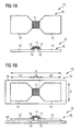
- FIG. 1A shows an exemplary embodiment of a portable object 10 in a cross-section and in a top view.
- the portable object 10 comprises an integrated circuit 11 and a first and a second pad 12, 13.
- the integrated circuit 11 is directly electrically connected to the first and the second pad 12, 13.
- the integrated circuit 11 comprises a first and a second RF pad 14, 15.
- the portable object 10 comprises a first and a second conductive glue spot 16, 17.
- the integrated circuit 11 is mechanically and electrically connected to the first pad 12 via the first RF pad 14 and the first conductive glue spot 16 and additionally to the second pad 13 via the second RF pad 15 and the second conductive glue spot 17.
- the coupling of the integrated circuit 11 to the first and the second pad 12, 13 is configured such that a DC electrical current can flow from the integrated circuit 11 to the first and the second pad 12, 13.
- the first and the second pad 12, 13 are arranged on opposite edges of the integrated circuit 11. In the top view, the area of the first pad 12 has a larger size in comparison to the area of the integrated circuit 11. Moreover, the area of the second pad 13 has a larger size in comparison to the area of the integrated circuit 11.
- the first and the second pad 12, 13 have approximately the same size.
- the areas of the first and the second pad 12, 13 basically have a rectangular form.
- the first and the second pad 12, 13 contain a metal, such as aluminium or copper.
- a strap 18 comprises the integrated circuit 11 and the first and the second pad 12, 13.
- FIG 1B shows a further exemplary embodiment of the portable object 10 which is a further development of the portable object shown in Figure 1A .
- the integrated circuit 11 and the first and the second pad 12, 13 are attached to a carrier 19 of the portable object 10.
- the carrier 19 is realized as an isolating carrier.
- the carrier 19 is nonconductive.
- the carrier 19 is made of dielectric insulating material.
- the carrier 19 contains a material such as PTFE or PET.
- the first and the second pad 12, 13 are directly arranged on the carrier 19.
- the carrier 19 has a rectangular form.
- the carrier 19 is realized as a sheet.
- the carrier 19 may be fabricated from a flexible foil.
- the carrier 19 is flexible.
- the strap 18 comprises the carrier 19.
- the carrier 19 acts as a basis for the first and the second pad 12, 13 and the integrated circuit 11.
- the first and the second pad 12, 13 and the integrated circuit 11 have a first extension A and a second extension B.
- the second extension B is smaller than the first extension A.
- the second extension B is the width of the first pad 12 and the second pad 13.
- the first extension A is the sum of an extension A1 of the first pad 12, an extension A2 of the integrated circuit 11 and an extension A3 of the second pad 13.
- the strap 18 is realized as a RFID strap or RFID tag.
- the integrated circuit 11 is fabricated as a die or chip.
- the integrated circuit 11 is implemented as a microchip.
- the size of the integrated circuit 11 may be less than 1 mm square.
- the pads 12, 13 are conductive parts and are fabricated from a metallization layer.
- the pads 12, 13 can be named conductive contact parts.
- the pads 12, 13 are etched, printed or attached on the carrier 19.
- the integrated circuit 11 is attached to the pads 12, 13 by using electrically conductive glue spots 16, 17.
- the integrated circuit 11 is flip-chip mounted on the carrier 19.
- the strap 18 can be fabricated by high-speed roll-to-roll manufacturing. Typical dimensions of the strap 18 are for example 10mm x 2.5mm with side pads 12, 13 of 2.5mm x 3mm.
- the strap 18 is used to ease the assembling.
- oversized pads 12, 13 the attachment of the RFID integrated circuit 11 to another body is simplified.
- the microchip is a very small component with tiny contact pads that have to be very precisely placed on an antenna. This can be a relatively slow process.
- the portable object 10 comprises at least a further pad which is connected to the integrated circuit 11.
- FIG 2A shows an exemplary embodiment of an information transmission system 30 in a cross-section and in a side view.
- the portable object 10 additionally comprises an item 31 on which the strap 18 is arranged.
- the integrated circuit 11, the first and the second pad 12, 13 are arranged on the item 31.
- the information transmission system 30 comprises the portable object 10 and a signal transfer arrangement 32.
- the signal transfer arrangement 32 is designed for signal and energy transfer to the portable object 10.
- the signal transfer arrangement 32 comprises a first and a second conducting line 33, 34.
- the first and the second conducting line 33, 34 form a transmission line.
- the first and the second conducting line 33, 34 are straight or linear lines.
- the first and the second conducting line 33, 34 have a main direction.
- the signal transfer arrangement 32 comprises a carrier body 35 on which the first and the second conducting line 33, 34 are attached.
- the carrier body 35 is a flexible body or a rigid body.
- the carrier body 35 is non-conductive.
- the carrier body 35 can be a printed circuit board, abbreviated PCB, or a flexible circuit.
- the first and the second conducting line 33, 34 are parallel. As also illustrated in Figure 1B , the first and the second pad 12, 13 and the integrated circuit 11 have the first extension A.
- the first and the second conducting line 33, 34 have a distance D.
- the two conducting lines 33, 34 are separated by the distance D.
- the first conducting line 33 has a width W and a length L.
- the second conducting line 34 has approximately the same width W and the same length L.
- the first pad 12 is capacitively coupled to the first conducting line 33 via an air gap 29.
- the second pad 13 is capacitively coupled via the air gap 29 to the second conducting line 34.
- the first pad 12 and the first conducting line 33 overlap such that a first parallel capacitor 97 is formed by the first pad 12 and the first conducting line 33.
- the overlap of the second pad 13 and of the second conducting line 34 results in a second parallel capacitor 98 formed by the second pad 13 and the second conducting line 34.
- Due to the length L of the first and the second conducting line 33, 34 the portable object 10 can be placed on a plurality of sites on the first and the second conducting line 33, 34.
- the length L is larger than the second extension B of the first pad 12.
- the length L is larger than the width W of the first conducting line 33.
- the portable object 10 can also move in the main direction of the first and the second conducting line 33, 34 without losing the electrical coupling between the first and the second pad 12, 13 and the first and the second conducting line 33, 34.
- FIG. 2B is a further exemplary embodiment of the information transmission system 30 which is a further development of the embodiments shown in Figures 1A, 1B and 2A .
- the first and the second conducting line 33, 34 are arranged at a first surface of the carrier body 35.
- the first surface of the carrier body 35 is flat.
- An insulating layer 37 is fabricated on the first and the second conducting line 33, 34.
- Thelayer 37 covers the first and the second conducting line 33, 34 and the first surface of the carrier body 35.
- the portable object 10 is arranged on the first surface of the carrier body 35.
- the portable object 10 comprises the carrier 19, wherein the carrier 19 is arranged between the first and the second conducting line 33, 34 and the first and the second pad 12, 13.
- the first pad 12 is isolated by the carrier 19, the air gap 29 and the isolating layer 37 from the first conducting line 33.
- the second pad 12 is isolated by the carrier 17, the air gap 29 and the isolating layer 37 from the second conducting line 34.
- the portable object 10' can alternatively be arranged at a second surface of the carrier body 35 that is opposite to the first surface of the carrier body 35.
- the upper part illustrates the two sites where the portable object 10, 10' can be placed. In general, only one of the two objects, either the portable object 10 or the portable object 10', is attached at the signal transfer arrangement 32.
- the first and the second conducting line 33, 34 are implemented as two parallel traces that form a transmission line.
- the first and the second conducting line 33, 34 are parallel to each other such as two rails of a railway.
- the strap 18 is coupled to the transmission line.
- the strap 18 is used without any connection to an antenna.
- the strap 18 is capacitively coupled to the transmission line, thus no electrical connection is needed.
- the strap 18 can be named a tag or a RFID tag.
- the communication between a not shown RFID reader 80 and the strap 18 occurs through signal propagation along the transmission line and capacitive coupling to the strap 18.
- the transmission line and the strap 18 are isolated by dielectric materials (solder mask / solder block or the substrate 35 itself of the transmission line, plus the PTFE or PET coating 19 of the strap 18).
- the strap 18 can be placed either direct on top of the transmission line or on the back side of the carrier body 35. Between the transmission line and the pads 12, 13 only dielectric layers are present.
- the transmission line can be implemented on rigid PCB
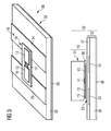
- FIG 3 shows a further exemplary embodiment of the information transmission system 30.
- a conducting layer 38 is fabricated on the second surface of the carrier body 35.
- the conducting layer 38 contains a metal.
- the portable object 10 is located at the first surface of the carrier body 35.
- the carrier body 35 is realized as a PCB.
- the conducting layer 38 forms a ground plane.
- the transmission line is formed by two parallel traces realized by the first and the second conducting line 33, 34 and the ground plane implemented by the conducting layer 38.
- the strap 18 is coupled to the transmission line.
- the strap 18 can not be placed on the second surface of the carrier body 35 that means the bottom side of the PCB and can only be placed on top of it, in order to be able to couple in an efficient way with the transmission line.
- FIG. 4 shows a further exemplary embodiment of the information transmission system 30 which is a further development of the above-shown embodiments.
- a third conducting line 39 is arranged on the carrier body 35.
- the first conducting line 33 is between the third conducting line 39 and the second conducting line 34.
- the third conducting line 39 has a distance D' to the first conducting line 33.
- the distance D' between the first and the third conducting line 33, 39 is equal to the distance D between the first and the second conducting line 33, 34.
- the first, the second and the third conducting line 33, 34, 39 also form a transmission line.
- the signal transfer arrangement 32 comprises the third conducting line 39.
- the first, the second and the third conducting line 33, 34, 39 are implemented as a coplanar waveguide, abbreviated CPW.
- the signal transfer arrangement 32 comprises the CPW.
- the conducting line which is in the middle between the other two conducting lines is a signal line.
- the outer conducting lines are ground reference lines.
- the first conducting line 33 is the signal line and the second and the third conducting line 34, 39 are the ground reference lines.
- the portable object 10 can be attached to the first surface or, alternatively, to the second surface of the carrier body 35.
- the strap 18 is coupled to the CPW.
- the center trace is the signal line and the side traces are the ground reference line. Due to field distribution in the CPW, in order to achieve efficient coupling between the strap 18 and the transmission line, the strap 18 has to be placed between the signal line and one of the ground reference lines.
- the strap 18 can be located direct on top of the traces or on bottom side of the PCB respectively flexible circuit 35.
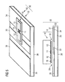
- FIG. 5 shows a further exemplary embodiment of the information transmission system 30 which is a further development of the above-shown embodiments.
- the conducting layer 38 is fixed on the second surface of the carrier body 35.
- the third conducting line 39 is fabricated on the first surface of the carrier 35.
- the portable object 10 can only be attached to the first surface of the carrier body 35.
- the portable object 10 can be arranged such that the first and the second pad 12, 13 are capacitively coupled to the first and the second conducting line 33, 34, but the portable object 10 can alternatively also be arranged such that the first and the second pad 12, 13 are capacitively coupled to the first and the third conducting line 33, 39.
- the coplanar waveguide is realized as a grounded CPW, abbreviated GCPW. In case of grounded CPW due to presence of the ground layer 38 under the carrier body 35, the strap 18 can be placed only on top of the carrier body 35.
- Figure 6 shows a further exemplary embodiment of the information transmission system 30 which is a further development of the above-shown embodiments.
- the first and the second conducting line 33, 34 are curved.
- the first and the second conducting line 33, 34 may have the form of a half-circle, a circle arc or a circle.
- the first surface of the carrier body 35 can have a three-dimensional form.
- the carrier body 35 can have the form of a cylinder, cone, hemisphere or another non-flat three-dimensional form.
- the two parallel traces 33, 34 forming the transmission line are fixed on a circular substrate 35 with or without ground 38.
- the transmission line configuration having the two traces 33, 34 do not follow a straight line direction, but follow a curved path on a plane of the carrier body 35.
- FIG. 7 shows a further exemplary embodiment of the information transmission system 30 which is a further development of the above-shown embodiments.
- the third conducting line 39 is arranged on the first surface of the carrier body 35.
- a coplanar waveguide is attached to the three-dimensional and non-flat carrier body 35.
- the CPW is realized on a circular substrate 35 with or without ground 38 and the strap 18 is coupled to it.
- the CPW is implemented as a curved CPW.
- the strap 18 has to be placed between the signal and the ground line to ensure correct coupling.
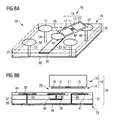
- FIG 8A shows a further exemplary embodiment of the information transmission system 30 which is a further development of the above-shown embodiments.
- the signal transfer arrangement 32 comprises the first conducting line 33, the carrier body 35 and the insulating layer 37.
- the signal transfer arrangement 32 comprises a further pad 45 which is on the top surface of the insulating layer 37 and is connected to the first conducting line 33 by a via 46.
- the signal transfer arrangement 32 also comprises an additional pad 47 that is on the top surface of the insulating layer 37 and is connected by a further via 48 to the conducting layer 38.
- the further pad 45 and the additional pad 47 have such a distance that the first and the second pad 12, 13 can couple to the further and the additional pad 45, 47.
- the second conducting line 34 can be implemented by the conducting layer 38.
- the conducting layer 38 in Figures 8A to 8C has the same function as the second conducting line 34 in Figures 2 to 7 .
- the portable object 10 is arranged on the signal transfer arrangement 32 such that the portable object 10 can communicate to the first conducting line 33 and the conducting layer 38 by means of the further and the additional pad 45, 47.
- the signal transfer arrangement 32 comprises three more additional pads 49 to 51 which are electrically connected to the conducting layer 38 by further vias 52 to 54.
- the additional pads 47, 49, 50, 51 are arranged such that they are located at the corners of a rectangular area on the first surface of the signal transfer arrangement 32, wherein the further pad 45 is in the middle of the rectangular area.
- the isolating layer 37, the first conducting line 33, the carrier body 35 and the conducting layer 38 can be realized as parts of a PCB.
- the PCB can be implemented as a multi-layer PCB.
- the carrier body 35 and the isolating layer 39 can be formed by isolating layers of the multi-layer PCB.
- the first conducting line 33 and the conducting layer 38 can be fabricated as metallization layers of the multi-layer PCB.
- the distance of the further pad 45 to the additional pads 47, 49, 50, 51 is approximately equal.
- the portable object 10 can be attached to four different sites on the first surface of the signal transfer arrangement 32 for communication.
- the first conducting line 33 and the conducting layer 38 form a strip-line.
- the strip-line in a multilayer structure including the pads 45, 47, 49, 50, 51 connected to signal and ground plane creates an ad-hoc electric field distribution in order to allow coupling between the strip-line and the strap 18. Coupling between the strap 18 and signal propagating through the transmission line is implemented by the pads 45, 47, 49, 50, 51 that are placed in a different layer with respect to the signal line 33 and the ground 38.
- the pads 45, 47, 49, 50, 51 are connected to the signal line 33 and to the reference ground 38.
- Figure 8B shows a cross-section of the information transmission system 30 shown in Figure 8A .
- the pads 45, 47, 49, 50, 51 can have a circular shape, a rectangular shape, a quadratic shape or any other shape.
- the via 53 is located such that it connects the middle of the additional pad 50 the conductive layer 38.
- the via can connect another point of the pad, for example it can connect an edge of the pad to the conducting layer 38, as shown by the additional pad 49 and the via 52 on the right-hand side of the cross-section shown in Figure 8B .
- the signal transfer arrangement 32 comprises pads 45, 47, 49, 50, 51 that are used to couple with the strap 18 and placed in a different layer.
- the center pad 45 is electrically connected to the signal line 33 and the surrounding pads 47, 49, 50, 51 are connected to the signal reference ground 38.
- the strap 18 is not directly electrically connected to the pads 45, 47, 49, 50, 51 but separated by a further insulating layer 44. This configuration is advantageous, when a high integration is needed.
- the signal transfer arrangement 32 can comprise at least a further layer under the reference ground layer 38, where at least an electronic device is placed.
- the electronic device can be a RFID Reader integrated circuit or an interface to a network or to a personal computer.
- the additional pads 47, 49 to 51 are electrically connected to the second conducting line 34 by the further vias 48, 52 to 54.
- FIG 8C shows a further exemplary embodiment of the information transmission system 30 which is a further development of the embodiment shown in Figures 8A and 8B .
- the information transmission system 30 comprises more than one of the unit 55 of the signal transfer arrangement 32 shown in Figure 8A .
- the unit 55 shown in Figure 8A comprises the further pad 45 that is connected to the first conducting line 33 and at least one additional pad 47, 49, 50, 51.
- the signal transfer arrangement 32 of Figure 8C comprises a plurality of units 55, each having a pad connected to a conducting line and at least one additional pad connected to the conducting layer 38.
- the conducting lines of the different units 55 to 60 are connected to the same conducting line which is the first conducting line 33.
- the strap 18 can be placed on the first surface of the signal transfer arrangement 32 on several sites for communication.
- the signal transfer arrangement 32 can be interconnected with another signal transfer arrangement for enhancing the reading area.
- the conducting lines of the different units 55-60 are not connected to each other.
- a strap 18 located on the signal transfer arrangement 32 may selectively communicate to different conducting lines.
- the portable object 10 may comprise more than one strap 18.
- the portable object 10 may be arranged on top of the first surface of the signal transfer arrangement 32 such that the plurality of straps 18 communicate to the plurality of units 55 to 60 of the signal transfer arrangement 32.
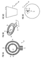
- FIGS 9A to 9D show a further exemplary embodiment of the information transmission system 30 which is a further development of the above-shown embodiments.
- the portable object 10 is realized as a container 70.
- the container 70 can be implemented as a capsule 71.
- the capsule 71 contains a liquid.
- the capsule 71 is realized as a coffee capsule or coffee pod or coffee pad.
- the strap 18 is arranged at the outside of the container 70.
- the strap 18 is arranged near the top of the container 70.
- the information transmission system 30 comprises a fluid dispensing system 72, not shown, which comprises the signal transfer arrangement 32.
- the fluid dispensing system 72 is implemented as a coffee machine 72'.
- the signal transfer arrangement 32 is designed such that it has a hole 76 for inserting the container 70.
- the first and the second conducting line 33, 34 are arranged in a circular form.
- the signal transfer arrangement 32 comprises a feeding point 73 for providing contact to the first and the second conducting line 33, 34.
- the signal transfer arrangement 32 comprises a termination 74.
- the termination 74 provides that the transmission line realized by the first and the second conducting line 33, 34 obtains its characteristic impedance value.
- Figure 9A shows the top view on the signal transfer arrangement 32
- Figure 9B shows a three-dimensional view on the signal transfer arrangement 32.
- the side view of the container 70 is shown in Figure 9C
- a top view of the container 70 is illustrated by Figure 9D .
- the transmission line configuration is able to read the strap 18 mounted on the capsule 71.
- the information transmission system 30 can be implemented in or by the coffee machine 72'.
- An initial CPW matched to a not-shown RF cable 79 and consequently to the reader 80 is split into two branches having characteristic impendence that keep the transmission line matched at the splitting point dividing the power received from reader 80 by two and distributing it to the two branches of the transmission line.
- the structure is circular like all the majority of capsules 71 and has the hole 76 in the middle needed to allow to the coffee machine 72' to operate correctly.
- a series of needles are normally placed in the middle of the capsule 71 to pump water into it and allow coffee brewing.
- the capsule 71 is equipped on top of it with the strap 18 in a way that the strap 18 will be aligned with the two traces 33, 34 during operation.
- Figures 10A to 10C show a further exemplary embodiment of the information transmission system 30 which is a further development of the above-shown embodiments.
- Figure 10 shows a schematic view of the fluid dispensing system 72, which is implemented as the coffee machine 72'.
- the container 70 is not attached to the fluid dispensing system 72.
- the portable object 10 does not couple to the first and the second transmission line 33, 34.
- the portable object 10 is in close proximity to the fluid dispensing system 72.
- the portable object 10 is arranged to the signal transfer arrangement 32 such that the first and the second pad 12, 13 are capacitively coupled to the first and the second conducting line 33, 34 for data transmission.
- the coffee machine 72 communicates with the container 70, for example, the information transmission system 30 recognizes for which drink or which sort of coffee or coffee-based mixture the container 70 is foreseen.
- the coffee machine 72 provides the coffee or coffee based mixture to a cup 69 through a tube 68.
- a second phase of operation the container 70 is detached from the fluid dispensing system 72.
- the portable object 10 is removed from the signal transfer arrangement 32 and, therefore, the first and the second pad 12, 13 are detached from the first and the second conducting line 33, 34.
- a user can take the cup 69 for drinking and the capsule 71 is removed from the coffee machine 72'.
- the second phase of operation can be illustrated by Figure 10A . The difference is that the capsule 71 is empty and the cup 69 is filled in the second phase of operation.
- the integrated circuit 11 comprises a memory 106 with a number.
- the fluid dispensing system 72 is configured to receive the number via the signal transfer arrangement 32 and to select one of several methods of operation of the fluid dispensing system 72 according to this number. In the different methods of operation, the fluid dispensing system 72 dispenses different drinks or brews different sorts of coffee or coffee-based mixtures.
- the memory 106 of the integrated circuit 11 stores the information regarding which drink, which kind of coffee or coffee-based mixture is wanted by the user.
- the fluid dispensing system 72 receives this information via the signal transfer arrangement 32 and selects the appropriate method of operation for providing the specified drink or sort of coffee or coffee-based mixture.
- the transmission line as shown in Figure 9 is mounted on the coffee machine 72'.
- the transmission line described in the Figures above is connected to the RFID reader 80 via the RF cable 79 and is embedded into the coffee machine 72' exactly in the area, where the capsule 71 will be in contact with needles in order to allow brewing.
- the capsule 71 is placed into the holder 77 and by means of a mechanical system, manually or automatic, will be coupled with the needles and consequently the transmission line will be coupled with the strap 18 placed on top of the capsule 71.
- the first phase of operation starts during which the reader 80 is able to identify the capsule 71 and read out information from the RFID integrated circuit tag.
- the information received from the RFID tag will be transferred to the central processing unit, abbreviated CPU, of the coffee machine 72' and the coffee machine 72' will enable (if the container 70 or the capsule 71 is the proper one) the brewing of the correct coffee based mixtures / drink or any other drink without any selection from the user.
- the user will need only to start the information transmission system 30 that incorporates the coffee machine 72' and said system 30 will select the proper brewing configuration automatically according with the identified container 70.
- the reader 80 will recognize that the container 70 is not present any more and will send the information regarding the non-presence to the CPU that will place the coffee machine 72' in stand by mode.
- the CPU of the coffee machine 72' is a microcontroller.
- FIG 11 shows an alternative embodiment of the information transmission system 30 which is a further development of the above-shown embodiments.
- the strap 18 is arranged in the lower half of the container 70.
- the first and the second conducting line 33, 34 have an approximately circular form. However, the first and the second conducting line 33, 34 do not comprise a complete circle.
- the end 75 of the first conducting line 33 is coupled to the end 75' of the second conducting line 34 via the termination 74.
- the parallel trace transmission line can be placed around the holder 77 of the container 70 and the strap 18 is placed on the side of the container 70. When the container 70 is placed into the machine holder 77, the strap 18 is aligned with the transmission line and couples with it.
- Figure 12 shows an alternative embodiment of the information transmission system 30 which is a further development of the above-shown embodiments.
- the container 70 is inserted into the holder 77.
- the signal transfer arrangement 32 is arranged on the outside of the holder 77.
- the first and the second conducting line 33, 34 are attached at the outside of the holder 77.
- the holder 77 has such a form that the strap 18 on the container 70 is brought into close vicinity to the first and the second conducting line 33, 34.
- the container 70 and the holder 77 are fabricated such that the two pads 12, 13 are capacitively coupled to the two conducting lines 33, 34.
- the first and the second conducting line 33, 34 have an approximately circular form.
- the container 70 has a rotational symmetry to a middle axis 78.
- the strap 18 does not have to be fixed on exactly one site to achieve a communication between the integrated circuit 11 and the coffee machine 72'.
- the coffee machine 72' is able to communicate with the container 70 at different angles of rotation of the container 70 related to the middle axis 78.
- the parallel trace transmission line is designed to be able to read the strap 18 mounted on the side of the container 70.
- the parallel traces are placed on the coffee machine 72' in order to be able to read the strap 18 placed on the side of the container 70.
- the system works as described in Figure 11 .
- the transmission line is now placed inside the container holder 77 and the information transmission system 30 will be able to identify the container 70 immediately after it will be placed into the machine 72. This takes place, before the container 70 will be coupled with needles.
- the portable object 10 may be realized as food or beverage container comprising the strap 18.
- the portable object 10 is realized as the cup 69 comprising the strap 18.
- the cup 69 may be a coffee cup.
- the coffee machine 72' may comprise the signal transfer arrangement 32 at the place, where the cup 69 is applied by the user.
- the coffee machine 72' identifies the cup 69 in the first phase of operation and provides the desired drink such as soft-drink, tea, coffee or coffee-based mixture.
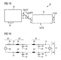
- FIG 13 shows an exemplary embodiment of an electronic system comprised by the information transmission system 30 shown above.
- the information transmission system 30 comprises the signal transfer arrangement 32, the cable 79 and the reader 80.
- the signal transfer arrangement 32 comprises the transmission line.
- the transmission line can be realized as a CPW, a grounded CPW, a strip line or another type of transmission line.
- the signal transfer arrangement 32 is configured to be coupled to the strap 18 of the portable object 10.
- the transmission line has a termination 74 on one end of the transmission line and is connected on its other side to the cable 79.
- the cable 79 is realized as an RF cable.
- the cable 79 couples the signal transfer arrangement 32 to the reader 80.
- An input 81 of the reader 80 to which the cable 79 is connected is realized as an RF input/output.
- the input 81 has a characteristic impedance Z RF .
- the cable 79 has a characteristic impedance Z cable .
- the transmission line has a characteristic impedance Z O .
- the termination 74 also has a characteristic impedance Z L .
- the impedances at interfaces are complex conjugate to each other.
- the impedance Z L of the termination 74 is complex conjugate to the impedance Z O of the transmission line at the end 75, 75' of the transmission line.
- the impedance Z O of the transmission line is complex conjugate to the impedance Z cable at the feeding point 73.
- the impedance Z RF is complex conjugate to the impedance Z cable at the input 81.
- the reader 80 can be implemented as a RFID reader.
- the reader 80 comprises a communication interface 82.
- the communication interface 92 of the reader 80 can be foreseen for communication with a personal computer, Universal Serial Bus - abbreviated USB -, Inter-Integrated Circuit bus - abbreviated I2C bus - , Serial Peripheral Interface bus - abbreviated SPI bus - , a network, a controller or a middleware system.
- the RFID reader 80 is connected via the RF cable 79 to the transmission line 32 terminated on a load impedance 74.
- the transmission line is designed in a way to allow capacitive coupling between the strap 18 and itself as well as has a geometrical configuration able to achieve fully matching between the cable 79 and itself, in order to transfer all the power provided by the reader 80 to the signal line 33 and consequently to the strap 18.
- Figure 14 shows an exemplary embodiment of a model of the signal transfer arrangement 32 shown above.
- the first conducting line 33 is modelled by a series connection of units 83, 84.
- Each unit 83, 84 comprises an inductor 85 and a capacitor 86.
- the inductors 85 of the first conducting line 33 are connected in series, whereas the capacitors 86 connect a node between the inductors 85 to a reference potential terminal 87.
- the second conducting line 34 also comprises several units which can be modelled as the units 83, 84 of the first conducting line 33.
- the end 75 of the first conducting line 33 and the end 75' of the second conducting line 34 are connected to each other via the termination 74.
- the reader 80 is modelled by a signal generator 88 and a resistor 89 which are series connected.
- the series connection of the signal generator 88 and the resistor 89 are arranged between the input terminal of the first conducting line 33 and the input terminal of the second conducting line 34.
- FIG 14 a simplified circuital model of the parallel trace transmission line is shown.
- the parameters of the transmission line configuration such as trace width W, inter-distance D (distance between two different traces) and dielectric substrate properties and thickness are selected in a way to allow perfect matching between the reader 80 and the conducting lines 33, 34. This will allow transferring all the power from the reader 80 to the transmission line and maximizing the coupling with the strap 18.
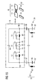
- Figure 15 shows an exemplary embodiment of an equivalent circuit of the strap 18 and of the signal transfer arrangement 32.
- the integrated circuit 11 can be modelled as a parallel circuit of a resistor 90 and a capacitor 91.
- the capacitor 91 obtains a value of few pF, whereas the resistor 90 has a few KQ.
- the first pad 12 and its connection to the integrated circuit 11, for example by the first conductive glue spot 16, can be modelled as a parallel circuit of an inductor 92 and a capacitor 93.
- the inductor 92 has a value of pH.
- a similar model can be chosen for the second pad 13.
- a further capacitor 94 is arranged between the outer terminals 95, 96 of the first and the second pad 12, 13.
- the strap 18 When the strap 18 is placed in proximity to the transmission line, a capacitance between the two pads 12, 13 and the two conducting lines 33, 34 is created and said capacitance allows power transfer between the transmission line and the two pads 12, 13 and consequently to the integrated circuit 11.
- the coupling of the first and the second pad 12, 13 to the first and second conducting line 33, 34 can be modelled by the first coupling capacitor 97 between the outer terminal 95 of the first pad 12 and the first conducting line 33.
- the coupling is modelled by the second coupling capacitor 98 between the outer terminal 96 of the second pad 12 and the second conducting line 34.
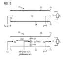
- Figure 16 shows an exemplary embodiment of a model of the signal transfer arrangement 32 with and without strap 18.
- the signal transfer arrangement 32 comprises a matched transmission line.
- the matched transmission line comprises the first and the second conducting line 33, 34 and the termination 74.
- the signal transfer arrangement 32 is shown with the strap 18 which couples the first to the second conducting line 33, 34.
- the strap 18 causes a reflected signal SREF.
- the reflected signal SREF is provided to the reader 80 and is used for receiving information from the integrated circuit 11.
- the information transmission system 30 uses a backscatter principle for communication by means of the transmission line with the strap 18 coupled to it.
- the reader 80 sends a carrier wave, abbreviated CW, at a well defined frequency to transfer energy to the strap 18 with the integrated circuit 11 and information by modulating the carrier wave CW by using Amplitude Shift Keying modulation or Phase-Shift Keying modulation, abbreviated ASK and PSK.
- CW carrier wave
- ASK and PSK Phase-Shift Keying modulation
- the strap 18 is able to receive the power transmitted by the reader 80, transform the CW in a quasi DC voltage by using a supply circuit 102, demodulate the command by a demodulator 104, perform some processing on a logic circuit 105 and answer to the request of the reader 80 by doing ASK or PSK modulation by means of a modulator 103.
- the modulation on the side of the integrated circuit 11 is done by switching the impedance of the integrated circuit 11 between two different states.
- the strap 18 When the strap 18 is transferred to the transmission line and capacitive coupling occurs, at a certain point of an original fully matched transmission line a load is placed by the strap 18 that will create reflection versus the reader 80.
- the level of the reflected signal SREF will change between the two modulation states of the integrated circuit 11.
- the reader 80 will be able to decode the ASK or PSK modulated signal by demodulating the reflected signal SREF received from the transmission line.
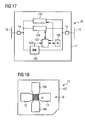
- FIG 17 shows an exemplary embodiment of the integrated circuit 11 which can be inserted in one of the above-shown information transmission systems 30.
- the integrated circuit 11 comprises the first and the second RF pad 14, 15 as well as the supply circuit 102 which is connected on its input side to the first and the second RF pad 14, 15.
- the first RF pad 14 is directly connected to the first pad 12, whereas the second RF pad 15 is directly connected to the second pad 13.
- the supply circuit 102 has a supply output for providing a supply voltage VDD.
- the supply voltage VDD is a quasi DC voltage.
- the supply circuit 102 comprises a rectifier.
- the supply circuit 102 comprises a voltage double system.
- the supply circuit 102 may comprise a multi stage charge pump.
- the supply circuit 102 transforms the signals at the first and the second pad 12, 13 into the supply voltage VDD.
- the integrated circuit 11 comprises the modulator 103 which is connected on its output side to the first and the second RF pad 14, 15.
- the integrated circuit 11 comprises the demodulator 104 which is connected on its input side to the first and the second RF pad 14, 15.
- the integrated circuit 11 comprises the logic circuit 105.
- the logic circuit 105 is realized as a digital signal processing unit.
- the logic circuit 105 is connected on its input side to the supply output of the supply circuit 102 for providing the supply voltage VDD to the logic circuit 105.
- the logic circuit 105 and the demodulator 104 demodulate signals provided via the first and second pad 12, 13 to the integrated circuit 11 and use the commands to perform logic calculations inside the logic circuit 105.
- the logic circuit 105 provides information by means of the modulator 103 and via the first and the second pad 12, 13 to the reader 80.
- the modulator 103 uses the ASK or PSK modulation principle.
- the modulator 103 obtains a first impedance value between the first and the second RF pad 14, 15 in a first modulation state and a second impedance value in a second modulation state.
- the integrated circuit 11 comprises the memory 106 that is connected to the logic circuit 105.
- the memory 106 stores a number of the integrated circuit 11.
- the memory 106 comprises a read only memory segment, abbreviated ROM, or a one-time programmable memory segment, abbreviated OTP.
- the memory 106 may store data received from the reader 80 via the first and the second pad 12, 13.
- the memory 106 may comprise an EEPROM segment.
- the integrated circuit 11 is designed as RFID integrated circuit transponder. Exactly one semiconductor body comprises the integrated circuit 11.
- the integrated circuit 11 comprises a sensor such as a temperature sensor.
- the integrated circuit 11 comprises an interface to another integrated circuit of the portable object 10.
- FIG 18 shows an additional exemplary embodiment of the portable object 10.
- the portable object 10 is realized as a card 107 that comprises the strap 18.
- the portable object 10 comprises at least a further pad 108, 109 which is connected to the integrated circuit 11.
- a strap 18 having three pads 12, 13, 108 can be connected with the signal transfer arrangement 32 having three conducting lines as shown for example in Figure 4 .
- a strap 18 having three or more pads can be connected with the signal transfer arrangement 32 having pads as shown for example in Figures 8A to 8C .
- the different pads 12, 13, 108, 109 may be used for different purposes.
- the first and the second pad 12, 13 are foreseen for receiving and sending data via the modulator 103 and demodulator 104.
- the further pads 108, 109 are designed for energy transfer to the integrated circuit 11.
- the further pads 108, 109 are connected to the supply circuit 102.
- the supply circuit 102 is not directly connected to the first and the second pad 12, 13.
- the above described information transmission system 30 and method to operate can be used not only for drink and food dispenser systems 72, but in general with any identification system that use an RFID or secure element placed on a tag or SIM card or SD, micro SD portable system and which needs to be interconnected with another unit such as a personal computer or a mobile device in order to be able to dispense/provide a certain service request by the user.
Landscapes
- Engineering & Computer Science (AREA)
- Physics & Mathematics (AREA)
- General Physics & Mathematics (AREA)
- Theoretical Computer Science (AREA)
- Microelectronics & Electronic Packaging (AREA)
- Computer Hardware Design (AREA)
- Artificial Intelligence (AREA)
- Computer Vision & Pattern Recognition (AREA)
- Computer Networks & Wireless Communication (AREA)
- Near-Field Transmission Systems (AREA)
Abstract
A portable object (10) comprises an integrated circuit (11), a first pad (12) that is mechanically and electrically connected to the integrated circuit (11) and a second pad (13) that is mechanically and electrically connected to the integrated circuit (11). The portable object (10) is designed for data transfer by capacitive coupling of the first pad (12) to a first conducting line (33) and of the second pad (13) to a second conducting line (34), when the portable object (10) is brought in vicinity to the first and the second conducting line (33, 34).
Description
- The present invention is related to a portable object and an information transmission system.
- Beverage containers that incorporate a tag for radiofrequency identification, abbreviated RFID, usually require the use of tags with loop antennas which are read by complex reader antennas.
- Documents
US 2012/0019417 A1 ,US 2011/0114647 A1 andUS 7,845,375 B2 show examples of beverage containers with tags. - It is an object of the present application to provide a portable object and an information transmission system with reduced size.
- This object is solved by a portable object according to claim 1 and an information transmission system according to claim 8. Preferred embodiments are presented in the respective dependent claims.
- In an embodiment, a portable object comprises an integrated circuit, a first pad that is mechanically and electrically connected to the integrated circuit and a second pad that is mechanically and electrically connected to the integrated circuit. The portable object is designed for data transfer by capacitive coupling of the first pad to a first conducting line and of the second pad to a second conducting line, when the portable object is brought in vicinity to the first and the second conducting line.
- It is an advantage that the two pads of the portable object are sufficient for data transfer and energy transfer. Thus, the size and the cost of an electronic component of the portable object can be reduced to a high extent.
- In an embodiment, the portable object has such a small weight and small size that a user can carry it.
- In an embodiment, the first and the second pad are arranged to the first and the second conducting line in a first phase of operation such that the first pad is capacitively coupled to the first conducting line and the second pad is capacitively coupled to the second conducting line for data transmission and the first and the second pad are detached from the first and the second conducting line in a second phase of operation that follows the first phase of operation.
- In an embodiment, the coupling of the first and the second pad to the first and the second conducting line is configured such that an AC current flows between the pads and the conducting lines and a DC current between the pads and the conducting lines is prevented.
- In an embodiment, the portable object comprises a strap that comprises the integrated circuit as well as the first and the second pad. The strap may be implemented as a RFID strap.
- In an embodiment, an area of the first pad has a larger size than an area of the integrated circuit. An area of the second pad has a larger size than the area of the integrated circuit.
- The first and the second pad may be essentially two-dimensional.
- The first and the second pad may be basically rectangular.
- In an embodiment, the first and the second pad are arranged on opposite edges of the integrated circuit.
- In an embodiment, the portable object comprises a carrier which is attached on the first and the second pad. The carrier is realized as an insulating layer. The carrier is arranged between the first pad and the first conducting line and between the second pad and the second conducting line. The carrier electrically isolates the pads from the conducting lines.
- In an embodiment, the integrated circuit comprises a supply circuit that is coupled to the first and the second pad, a modulator circuit that is coupled to the first and the second pad and a logic circuit that is coupled to a supply output of the supply circuit for power supply and to a control input of the modulator circuit. The integrated circuit may comprise an analog integrated circuit.
- The integrated circuit can be realized as a RFID chip.
- In an embodiment, the portable object is realized as an item of a group comprising a container, a capsule, a cup and a card. The container may be configured to contain beverage or food. The capsule may be designed for containing beverage or food. The capsule can be implemented as a coffee capsule, a coffee pod or a coffee pad. The card can be a part from a group comprising a chip card, a Subscriber Identify Module card, a System-Identification Module card, a memory card, a smart card, a signature card, a cash card and a credit card.
- The portable object can be a fast moving consumer good, abbreviated FMCG. The FMCG may be a product that is sold quickly and at relatively low cost. Examples include nondurable goods such as soft drinks, toiletries and grocery items.
- The portable object may be a small object containing an electrically conducting material such as a metal or a liquid. Alternatively, the portable object may be a small object free of an electrically conducting material.
- In an embodiment, an information transmission system comprises a portable object and a signal transfer arrangement. The portable object comprises an integrated circuit, a first pad that is mechanically and electrically connected to the integrated circuit and a second pad that is mechanically and electrically connected to the integrated circuit. The signal transfer arrangement comprises a first and a second conducting line such that selectively either the first pad capacitively couples to the first conducting line and the second pad capacitively couples to the second conducting line, when the portable object is in vicinity of the signal transfer arrangement, or the first and the second pad are decoupled from the first and the second conducting line, when the portable object is at a distance from the signal transfer arrangement.
- It is an advantage of the information transmission system that the first capacitor between the first pad and the first conducting line and the second capacitor between the second pad and the second conducting line are sufficient to provide energy from the signal transfer arrangement to the portable object and to transfer data from the portable object to the signal transfer arrangement. By means of the capacitive coupling, a small size of the portable object is sufficient.
- In an embodiment, the portable object is in vicinity of the signal transfer arrangement in the first state of operation. The portable object is at a distance from the signal transfer arrangement in the second state of operation.
- In an embodiment, the coupling of the first and the second pad to the first and the second conducting line is free of an adhesive.
- The first and the second conducting line can be parallel to each other.
- The first and the second conducting line can be essentially two-dimensional.
- In an embodiment, an extension of the first and the second pad is coordinated with an extension of the first and the second conducting line. For example, the first and the second pad and the first and the second conducting line have lateral extensions according to the equation:

- In an embodiment, the first and the second conducting line have a main direction. The signal transfer arrangement is designed such that the capacitive coupling of the first and the second pad to the first and the second conducting line is continued during a movement of the portable object in the main direction of the first and the second conducting line.
- In an embodiment, the first and the second conducting line are arranged on a non-flat surface of the signal transfer arrangement.
- The first and the second conducting line may have the form of circular arcs.
- In an embodiment, the information transmission system comprises a reader or host that is electrically connected to the first and the second conducting line. The reader respectively host is designed to transmit energy to the portable object and to receive data from the integrated circuit of the portable object. Optionally, the reader respectively host is designed to send data to the integrated circuit of the portable object.
- In an embodiment, the reader is a single-chip reader. The reader may comply with the HF and
UHF Gen 2 RFID standards. UHF is the abbreviation for ultra high frequency. The reader may alternatively be operating between 15 and 150 kHz. The method can be used at any frequency range. - In an embodiment, the signal transfer arrangement comprises an insulating layer attached to the first conducting line and at least one further pad electrically connected to the first conducting line by a via through the insulating layer. Moreover, the signal transfer arrangement may comprise a conductive layer. At least an additional pad may be electrically connected to the conductive layer or the second conducting line by a further via.
- In an embodiment, the first and the second conducting line form a transmission line.
- In an embodiment, the signal transfer arrangement comprises a third conducting line. The first, the second and the third conducting line form a coplanar waveguide.
- In an embodiment, the portable object is free from a loop antenna which is coupled to the first and the second pad. Moreover, the reader or host is free from a loop antenna which is designed for communication with the portable object.
- In an embodiment, the information transmission system is foreseen for wireless data transmission.
- In an embodiment, a method for communication comprises arranging a portable object and a signal transfer arrangement to each other in a first phase of operation such that a first pad of the portable object is capacitively coupled to a first conducting line of the signal transfer arrangement and a second pad of the portable object is capacitively coupled to a second conducting line of the signal transfer arrangement. The first and the second pad are electrically connected to an integrated circuit of the portable object and data are transferred between the integrated circuit and the two conducting lines. Moreover, the portable object is detached from the signal transfer arrangement in a second phase of operation that follows the first phase of operation.
- In an embodiment, the method and the information transmission system are configured for tagging, by using UHF RFID tag, of FMCGs, and are designed for reading UHF RFID antenna less tags of FMCGs. A complex reader antenna is not required. Also a special RFID transponder or tag antenna is not required. The RFID reader is able to communicate with the RFID transponder integrated circuit without use of antennas of the reader and of the tag. A communication between the reader and the tag is enabled by using an unbalanced transmission line connected to the RFID reader and the RFID transponder integrated circuit mounted on the strap having pads larger than a conventional RFID strap (for example 20-30% bigger pad area).
- In an embodiment, the information transmission system, the portable object and the method for communication allow to reduce costs in implementation of a RFID enabled solution in FMCGs, especially soft drink, coffee, and in general any hot and cold drink system based on a RFID authentication and/or identification of cups or capsules ID and type prior to dispense the selected drink. A space occupied by the antenna is not required any more and tag size can for example be reduced 60% or more in comparison to conventional tags. Tag costs are highly reduced by means of size reduction of the RFID tag.
- The following description of figures of exemplary embodiments may further illustrate and explain the invention. In so far as components, elements or devices correspond to one another in terms of their function in different figures, the description thereof is not repeated for each of the following figures.
-
Figures 1A and 1B show exemplary embodiments of a portable object. -
Figures 2A ,2B ,3 to7 ,8A to 8C ,9A to 9D ,10A to 10C ,11 and 12 show exemplary embodiments of an information transmission system. -
Figure 13 shows an exemplary embodiment of an electronic system comprised by an information transmission system. -
Figure 14 shows an exemplary embodiment of a model of a signal transfer arrangement. -
Figure 15 shows an exemplary embodiment of an equivalent circuit of a strap and of a signal transfer arrangement. -
Figure 16 shows an exemplary embodiment of a model of a signal transfer arrangement. -
Figure 17 shows an exemplary embodiment of an integrated circuit. -
Figure 18 shows an exemplary embodiment of a portable object. -
Figure 1A shows an exemplary embodiment of aportable object 10 in a cross-section and in a top view. Theportable object 10 comprises anintegrated circuit 11 and a first and asecond pad integrated circuit 11 is directly electrically connected to the first and thesecond pad integrated circuit 11 comprises a first and asecond RF pad portable object 10 comprises a first and a secondconductive glue spot integrated circuit 11 is mechanically and electrically connected to thefirst pad 12 via thefirst RF pad 14 and the firstconductive glue spot 16 and additionally to thesecond pad 13 via thesecond RF pad 15 and the secondconductive glue spot 17. The coupling of theintegrated circuit 11 to the first and thesecond pad circuit 11 to the first and thesecond pad - The first and the
second pad integrated circuit 11. In the top view, the area of thefirst pad 12 has a larger size in comparison to the area of theintegrated circuit 11. Moreover, the area of thesecond pad 13 has a larger size in comparison to the area of theintegrated circuit 11. The first and thesecond pad second pad second pad strap 18 comprises the integratedcircuit 11 and the first and thesecond pad -
Figure 1B shows a further exemplary embodiment of theportable object 10 which is a further development of the portable object shown inFigure 1A . Theintegrated circuit 11 and the first and thesecond pad carrier 19 of theportable object 10. Thecarrier 19 is realized as an isolating carrier. Thecarrier 19 is nonconductive. Thecarrier 19 is made of dielectric insulating material. Thecarrier 19 contains a material such as PTFE or PET. The first and thesecond pad carrier 19. Thecarrier 19 has a rectangular form. Thecarrier 19 is realized as a sheet. Thecarrier 19 may be fabricated from a flexible foil. Thecarrier 19 is flexible. Thestrap 18 comprises thecarrier 19. Thecarrier 19 acts as a basis for the first and thesecond pad integrated circuit 11. - The first and the
second pad integrated circuit 11 have a first extension A and a second extension B. The second extension B is smaller than the first extension A. The second extension B is the width of thefirst pad 12 and thesecond pad 13. The first extension A is the sum of an extension A1 of thefirst pad 12, an extension A2 of theintegrated circuit 11 and an extension A3 of thesecond pad 13. - The
strap 18 is realized as a RFID strap or RFID tag. Theintegrated circuit 11 is fabricated as a die or chip. Theintegrated circuit 11 is implemented as a microchip. The size of theintegrated circuit 11 may be less than 1 mm square. Thepads pads pads carrier 19. Theintegrated circuit 11 is attached to thepads integrated circuit 11 is flip-chip mounted on thecarrier 19. Thestrap 18 can be fabricated by high-speed roll-to-roll manufacturing. Typical dimensions of thestrap 18 are for example 10mm x 2.5mm withside pads - The
strap 18 is used to ease the assembling. By means ofoversized pads circuit 11 to another body is simplified. Contrary to that, in conventional flip-chip manufacturing the microchip is a very small component with tiny contact pads that have to be very precisely placed on an antenna. This can be a relatively slow process. - In an alternative, not shown embodiment, the
portable object 10 comprises at least a further pad which is connected to theintegrated circuit 11. -
Figure 2A shows an exemplary embodiment of aninformation transmission system 30 in a cross-section and in a side view. Theportable object 10 additionally comprises anitem 31 on which thestrap 18 is arranged. Thus, theintegrated circuit 11, the first and thesecond pad item 31. Theinformation transmission system 30 comprises theportable object 10 and asignal transfer arrangement 32. Thesignal transfer arrangement 32 is designed for signal and energy transfer to theportable object 10. Thesignal transfer arrangement 32 comprises a first and asecond conducting line second conducting line second conducting line second conducting line signal transfer arrangement 32 comprises acarrier body 35 on which the first and thesecond conducting line carrier body 35 is a flexible body or a rigid body. Thecarrier body 35 is non-conductive. Thecarrier body 35 can be a printed circuit board, abbreviated PCB, or a flexible circuit. The first and thesecond conducting line Figure 1B , the first and thesecond pad integrated circuit 11 have the first extension A. The first and thesecond conducting line lines first conducting line 33 has a width W and a length L. Thesecond conducting line 34 has approximately the same width W and the same length L. The extensions follow the equations:
- As shown in the cross-section, the
first pad 12 is capacitively coupled to thefirst conducting line 33 via anair gap 29. Also, thesecond pad 13 is capacitively coupled via theair gap 29 to thesecond conducting line 34. Thefirst pad 12 and thefirst conducting line 33 overlap such that a firstparallel capacitor 97 is formed by thefirst pad 12 and thefirst conducting line 33. The overlap of thesecond pad 13 and of thesecond conducting line 34 results in a secondparallel capacitor 98 formed by thesecond pad 13 and thesecond conducting line 34. Due to the length L of the first and thesecond conducting line portable object 10 can be placed on a plurality of sites on the first and thesecond conducting line first pad 12. The length L is larger than the width W of thefirst conducting line 33. Theportable object 10 can also move in the main direction of the first and thesecond conducting line second pad second conducting line -
Figure 2B is a further exemplary embodiment of theinformation transmission system 30 which is a further development of the embodiments shown inFigures 1A, 1B and2A . The first and thesecond conducting line carrier body 35. The first surface of thecarrier body 35 is flat. An insulatinglayer 37 is fabricated on the first and thesecond conducting line Thelayer 37 covers the first and thesecond conducting line carrier body 35. As shown on the left side of the lower part ofFigure 2B , theportable object 10 is arranged on the first surface of thecarrier body 35. Theportable object 10 comprises thecarrier 19, wherein thecarrier 19 is arranged between the first and thesecond conducting line second pad first pad 12 is isolated by thecarrier 19, theair gap 29 and the isolatinglayer 37 from thefirst conducting line 33. Correspondingly, thesecond pad 12 is isolated by thecarrier 17, theair gap 29 and the isolatinglayer 37 from thesecond conducting line 34. - As shown in the upper part and on the right side of the lower part of
Figure 2B , the portable object 10' can alternatively be arranged at a second surface of thecarrier body 35 that is opposite to the first surface of thecarrier body 35. The upper part illustrates the two sites where theportable object 10, 10' can be placed. In general, only one of the two objects, either theportable object 10 or the portable object 10', is attached at thesignal transfer arrangement 32. - The first and the
second conducting line second conducting line strap 18 is coupled to the transmission line. Thus, thestrap 18 is used without any connection to an antenna. Thestrap 18 is capacitively coupled to the transmission line, thus no electrical connection is needed. Thestrap 18 can be named a tag or a RFID tag. The communication between a not shownRFID reader 80 and thestrap 18 occurs through signal propagation along the transmission line and capacitive coupling to thestrap 18. The transmission line and thestrap 18 are isolated by dielectric materials (solder mask / solder block or thesubstrate 35 itself of the transmission line, plus the PTFE orPET coating 19 of the strap 18). Thestrap 18 can be placed either direct on top of the transmission line or on the back side of thecarrier body 35. Between the transmission line and thepads -
Figure 3 shows a further exemplary embodiment of theinformation transmission system 30. A conductinglayer 38 is fabricated on the second surface of thecarrier body 35. The conductinglayer 38 contains a metal. Theportable object 10 is located at the first surface of thecarrier body 35. Thecarrier body 35 is realized as a PCB. The conductinglayer 38 forms a ground plane. Thus, the transmission line is formed by two parallel traces realized by the first and thesecond conducting line layer 38. Thestrap 18 is coupled to the transmission line. In case of transmission line with ground plane insulation, due to physic / theory of electric field propagation, thestrap 18 can not be placed on the second surface of thecarrier body 35 that means the bottom side of the PCB and can only be placed on top of it, in order to be able to couple in an efficient way with the transmission line. -
Figure 4 shows a further exemplary embodiment of theinformation transmission system 30 which is a further development of the above-shown embodiments. Athird conducting line 39 is arranged on thecarrier body 35. Thefirst conducting line 33 is between thethird conducting line 39 and thesecond conducting line 34. Thethird conducting line 39 has a distance D' to thefirst conducting line 33. The distance D' between the first and thethird conducting line second conducting line - The first, the second and the
third conducting line signal transfer arrangement 32 comprises thethird conducting line 39. The first, the second and thethird conducting line signal transfer arrangement 32 comprises the CPW. The conducting line which is in the middle between the other two conducting lines is a signal line. The outer conducting lines are ground reference lines. According toFigure 4 , thefirst conducting line 33 is the signal line and the second and thethird conducting line Figure 4 , theportable object 10 can be attached to the first surface or, alternatively, to the second surface of thecarrier body 35. - The
strap 18 is coupled to the CPW. In the CPW, the center trace is the signal line and the side traces are the ground reference line. Due to field distribution in the CPW, in order to achieve efficient coupling between thestrap 18 and the transmission line, thestrap 18 has to be placed between the signal line and one of the ground reference lines. Thestrap 18 can be located direct on top of the traces or on bottom side of the PCB respectivelyflexible circuit 35. -
Figure 5 shows a further exemplary embodiment of theinformation transmission system 30 which is a further development of the above-shown embodiments. The conductinglayer 38 is fixed on the second surface of thecarrier body 35. Thethird conducting line 39 is fabricated on the first surface of thecarrier 35. Thus, theportable object 10 can only be attached to the first surface of thecarrier body 35. Theportable object 10 can be arranged such that the first and thesecond pad second conducting line portable object 10 can alternatively also be arranged such that the first and thesecond pad third conducting line ground layer 38 under thecarrier body 35, thestrap 18 can be placed only on top of thecarrier body 35. -
Figure 6 shows a further exemplary embodiment of theinformation transmission system 30 which is a further development of the above-shown embodiments. The first and thesecond conducting line second conducting line carrier body 35 can have a three-dimensional form. Thecarrier body 35 can have the form of a cylinder, cone, hemisphere or another non-flat three-dimensional form. The twoparallel traces circular substrate 35 with or withoutground 38. The transmission line configuration having the twotraces carrier body 35. -
Figure 7 shows a further exemplary embodiment of theinformation transmission system 30 which is a further development of the above-shown embodiments. Thethird conducting line 39 is arranged on the first surface of thecarrier body 35. Thus, a coplanar waveguide is attached to the three-dimensional andnon-flat carrier body 35. The CPW is realized on acircular substrate 35 with or withoutground 38 and thestrap 18 is coupled to it. The CPW is implemented as a curved CPW. As for the previous example, in case of CPW, thestrap 18 has to be placed between the signal and the ground line to ensure correct coupling. -
Figure 8A shows a further exemplary embodiment of theinformation transmission system 30 which is a further development of the above-shown embodiments. Thesignal transfer arrangement 32 comprises thefirst conducting line 33, thecarrier body 35 and the insulatinglayer 37. Moreover, thesignal transfer arrangement 32 comprises afurther pad 45 which is on the top surface of the insulatinglayer 37 and is connected to thefirst conducting line 33 by a via 46. Thesignal transfer arrangement 32 also comprises anadditional pad 47 that is on the top surface of the insulatinglayer 37 and is connected by a further via 48 to theconducting layer 38. Thefurther pad 45 and theadditional pad 47 have such a distance that the first and thesecond pad additional pad second conducting line 34 can be implemented by the conductinglayer 38. The conductinglayer 38 inFigures 8A to 8C has the same function as thesecond conducting line 34 inFigures 2 to 7 . - The
portable object 10 is arranged on thesignal transfer arrangement 32 such that theportable object 10 can communicate to thefirst conducting line 33 and theconducting layer 38 by means of the further and theadditional pad signal transfer arrangement 32 comprises three moreadditional pads 49 to 51 which are electrically connected to theconducting layer 38 byfurther vias 52 to 54. Theadditional pads signal transfer arrangement 32, wherein thefurther pad 45 is in the middle of the rectangular area. - The isolating
layer 37, thefirst conducting line 33, thecarrier body 35 and theconducting layer 38 can be realized as parts of a PCB. The PCB can be implemented as a multi-layer PCB. Thecarrier body 35 and the isolatinglayer 39 can be formed by isolating layers of the multi-layer PCB. Thefirst conducting line 33 and theconducting layer 38 can be fabricated as metallization layers of the multi-layer PCB. The distance of thefurther pad 45 to theadditional pads portable object 10 can be attached to four different sites on the first surface of thesignal transfer arrangement 32 for communication. - The
first conducting line 33 and theconducting layer 38 form a strip-line. The strip-line in a multilayer structure including thepads strap 18. Coupling between thestrap 18 and signal propagating through the transmission line is implemented by thepads signal line 33 and theground 38. Thepads signal line 33 and to thereference ground 38. By doing this an electric field is created between thefurther pad 45 connected to thesignal line 33 and theadditional pads Figure 8A as four different capacitors). When thestrap 18 is placed in between thefurther pad 45 connected to thesignal line 33 and one of theadditional pads ground layer 38, it capacitively couples to both pads and allow signal and energy transmission from thesignal line 33 to theintegrated circuit 11 and consequently communication between theRFID reader 80 and theintegrated circuit 11. -
Figure 8B shows a cross-section of theinformation transmission system 30 shown inFigure 8A . Thepads additional pad 50 theconductive layer 38. Alternatively, the via can connect another point of the pad, for example it can connect an edge of the pad to theconducting layer 38, as shown by theadditional pad 49 and the via 52 on the right-hand side of the cross-section shown inFigure 8B . - The
signal transfer arrangement 32 comprisespads strap 18 and placed in a different layer. Thecenter pad 45 is electrically connected to thesignal line 33 and the surroundingpads signal reference ground 38. Thestrap 18 is not directly electrically connected to thepads layer 44. This configuration is advantageous, when a high integration is needed. Thesignal transfer arrangement 32 can comprise at least a further layer under thereference ground layer 38, where at least an electronic device is placed. The electronic device can be a RFID Reader integrated circuit or an interface to a network or to a personal computer. - In an alternative, not shown embodiment, the
additional pads second conducting line 34 by thefurther vias -
Figure 8C shows a further exemplary embodiment of theinformation transmission system 30 which is a further development of the embodiment shown inFigures 8A and 8B . Theinformation transmission system 30 comprises more than one of theunit 55 of thesignal transfer arrangement 32 shown inFigure 8A . Theunit 55 shown inFigure 8A comprises thefurther pad 45 that is connected to thefirst conducting line 33 and at least oneadditional pad signal transfer arrangement 32 ofFigure 8C comprises a plurality ofunits 55, each having a pad connected to a conducting line and at least one additional pad connected to theconducting layer 38. As shown inFigure 8C , the conducting lines of thedifferent units 55 to 60 are connected to the same conducting line which is thefirst conducting line 33. Thus, thestrap 18 can be placed on the first surface of thesignal transfer arrangement 32 on several sites for communication. Thesignal transfer arrangement 32 can be interconnected with another signal transfer arrangement for enhancing the reading area. - In an alternative, not-shown embodiment, the conducting lines of the different units 55-60 are not connected to each other. Thus, a
strap 18 located on thesignal transfer arrangement 32 may selectively communicate to different conducting lines. Theportable object 10 may comprise more than onestrap 18. Theportable object 10 may be arranged on top of the first surface of thesignal transfer arrangement 32 such that the plurality ofstraps 18 communicate to the plurality ofunits 55 to 60 of thesignal transfer arrangement 32. -
Figures 9A to 9D show a further exemplary embodiment of theinformation transmission system 30 which is a further development of the above-shown embodiments. Theportable object 10 is realized as acontainer 70. Thecontainer 70 can be implemented as acapsule 71. Thecapsule 71 contains a liquid. Thecapsule 71 is realized as a coffee capsule or coffee pod or coffee pad. Thestrap 18 is arranged at the outside of thecontainer 70. Thestrap 18 is arranged near the top of thecontainer 70. Furthermore, theinformation transmission system 30 comprises afluid dispensing system 72, not shown, which comprises thesignal transfer arrangement 32. Thefluid dispensing system 72 is implemented as a coffee machine 72'. Thesignal transfer arrangement 32 is designed such that it has ahole 76 for inserting thecontainer 70. The first and thesecond conducting line signal transfer arrangement 32 comprises afeeding point 73 for providing contact to the first and thesecond conducting line signal transfer arrangement 32 comprises atermination 74. Thetermination 74 provides that the transmission line realized by the first and thesecond conducting line Figure 9A shows the top view on thesignal transfer arrangement 32, whereasFigure 9B shows a three-dimensional view on thesignal transfer arrangement 32. The side view of thecontainer 70 is shown inFigure 9C , whereas a top view of thecontainer 70 is illustrated byFigure 9D . - The transmission line configuration is able to read the
strap 18 mounted on thecapsule 71. Theinformation transmission system 30 can be implemented in or by the coffee machine 72'. An initial CPW matched to a not-shownRF cable 79 and consequently to thereader 80 is split into two branches having characteristic impendence that keep the transmission line matched at the splitting point dividing the power received fromreader 80 by two and distributing it to the two branches of the transmission line. The structure is circular like all the majority ofcapsules 71 and has thehole 76 in the middle needed to allow to the coffee machine 72' to operate correctly. A series of needles are normally placed in the middle of thecapsule 71 to pump water into it and allow coffee brewing. Thecapsule 71 is equipped on top of it with thestrap 18 in a way that thestrap 18 will be aligned with the twotraces -
Figures 10A to 10C show a further exemplary embodiment of theinformation transmission system 30 which is a further development of the above-shown embodiments.Figure 10 shows a schematic view of thefluid dispensing system 72, which is implemented as the coffee machine 72'. As shown inFigure 10A , before a first phase of operation, thecontainer 70 is not attached to thefluid dispensing system 72. During this phase of operation, theportable object 10 does not couple to the first and thesecond transmission line Figures 10B and 10C , theportable object 10 is in close proximity to thefluid dispensing system 72. Thus, in the first phase of operation, theportable object 10 is arranged to thesignal transfer arrangement 32 such that the first and thesecond pad second conducting line Figure 10B , thecoffee machine 72 communicates with thecontainer 70, for example, theinformation transmission system 30 recognizes for which drink or which sort of coffee or coffee-based mixture thecontainer 70 is foreseen. In a second sub-phase of the first phase of operation shown inFigure 10C , thecoffee machine 72 provides the coffee or coffee based mixture to acup 69 through atube 68. - In a second phase of operation, the
container 70 is detached from thefluid dispensing system 72. Theportable object 10 is removed from thesignal transfer arrangement 32 and, therefore, the first and thesecond pad second conducting line cup 69 for drinking and thecapsule 71 is removed from the coffee machine 72'. The second phase of operation can be illustrated byFigure 10A . The difference is that thecapsule 71 is empty and thecup 69 is filled in the second phase of operation. - The
integrated circuit 11 comprises amemory 106 with a number. Thefluid dispensing system 72 is configured to receive the number via thesignal transfer arrangement 32 and to select one of several methods of operation of thefluid dispensing system 72 according to this number. In the different methods of operation, thefluid dispensing system 72 dispenses different drinks or brews different sorts of coffee or coffee-based mixtures. - In an alternative embodiment, the
memory 106 of theintegrated circuit 11 stores the information regarding which drink, which kind of coffee or coffee-based mixture is wanted by the user. Thefluid dispensing system 72 receives this information via thesignal transfer arrangement 32 and selects the appropriate method of operation for providing the specified drink or sort of coffee or coffee-based mixture. - The transmission line as shown in
Figure 9 is mounted on the coffee machine 72'. The transmission line described in the Figures above is connected to theRFID reader 80 via theRF cable 79 and is embedded into the coffee machine 72' exactly in the area, where thecapsule 71 will be in contact with needles in order to allow brewing. Thecapsule 71 is placed into theholder 77 and by means of a mechanical system, manually or automatic, will be coupled with the needles and consequently the transmission line will be coupled with thestrap 18 placed on top of thecapsule 71. At this point of time the first phase of operation starts during which thereader 80 is able to identify thecapsule 71 and read out information from the RFID integrated circuit tag. The information received from the RFID tag will be transferred to the central processing unit, abbreviated CPU, of the coffee machine 72' and the coffee machine 72' will enable (if thecontainer 70 or thecapsule 71 is the proper one) the brewing of the correct coffee based mixtures / drink or any other drink without any selection from the user. The user will need only to start theinformation transmission system 30 that incorporates the coffee machine 72' and saidsystem 30 will select the proper brewing configuration automatically according with the identifiedcontainer 70. When thecontainer 70 is removed, thereader 80 will recognize that thecontainer 70 is not present any more and will send the information regarding the non-presence to the CPU that will place the coffee machine 72' in stand by mode. The CPU of the coffee machine 72' is a microcontroller. -
Figure 11 shows an alternative embodiment of theinformation transmission system 30 which is a further development of the above-shown embodiments. Thestrap 18 is arranged in the lower half of thecontainer 70. The first and thesecond conducting line second conducting line end 75 of thefirst conducting line 33 is coupled to the end 75' of thesecond conducting line 34 via thetermination 74. The parallel trace transmission line can be placed around theholder 77 of thecontainer 70 and thestrap 18 is placed on the side of thecontainer 70. When thecontainer 70 is placed into themachine holder 77, thestrap 18 is aligned with the transmission line and couples with it. -
Figure 12 shows an alternative embodiment of theinformation transmission system 30 which is a further development of the above-shown embodiments. As shown on the right side ofFigure 12 , thecontainer 70 is inserted into theholder 77. Thesignal transfer arrangement 32 is arranged on the outside of theholder 77. Thus, the first and thesecond conducting line holder 77. Theholder 77 has such a form that thestrap 18 on thecontainer 70 is brought into close vicinity to the first and thesecond conducting line container 70 and theholder 77 are fabricated such that the twopads lines second conducting line container 70 has a rotational symmetry to amiddle axis 78. Thus, thestrap 18 does not have to be fixed on exactly one site to achieve a communication between theintegrated circuit 11 and the coffee machine 72'. The coffee machine 72' is able to communicate with thecontainer 70 at different angles of rotation of thecontainer 70 related to themiddle axis 78. - The parallel trace transmission line is designed to be able to read the
strap 18 mounted on the side of thecontainer 70. The parallel traces are placed on the coffee machine 72' in order to be able to read thestrap 18 placed on the side of thecontainer 70. The system works as described inFigure 11 . The transmission line is now placed inside thecontainer holder 77 and theinformation transmission system 30 will be able to identify thecontainer 70 immediately after it will be placed into themachine 72. This takes place, before thecontainer 70 will be coupled with needles. - The
portable object 10 may be realized as food or beverage container comprising thestrap 18. - In an alternative, not shown embodiment, the
portable object 10 is realized as thecup 69 comprising thestrap 18. Thecup 69 may be a coffee cup. The coffee machine 72' may comprise thesignal transfer arrangement 32 at the place, where thecup 69 is applied by the user. The coffee machine 72' identifies thecup 69 in the first phase of operation and provides the desired drink such as soft-drink, tea, coffee or coffee-based mixture. -
Figure 13 shows an exemplary embodiment of an electronic system comprised by theinformation transmission system 30 shown above. Theinformation transmission system 30 comprises thesignal transfer arrangement 32, thecable 79 and thereader 80. Thesignal transfer arrangement 32 comprises the transmission line. The transmission line can be realized as a CPW, a grounded CPW, a strip line or another type of transmission line. Thesignal transfer arrangement 32 is configured to be coupled to thestrap 18 of theportable object 10. The transmission line has atermination 74 on one end of the transmission line and is connected on its other side to thecable 79. Thecable 79 is realized as an RF cable. Thecable 79 couples thesignal transfer arrangement 32 to thereader 80. Aninput 81 of thereader 80 to which thecable 79 is connected is realized as an RF input/output. Theinput 81 has a characteristic impedance ZRF. Thecable 79 has a characteristic impedance Zcable. The transmission line has a characteristic impedance ZO. Thetermination 74 also has a characteristic impedance ZL. In the ideal case, the impedances at interfaces are complex conjugate to each other. For example, the impedance ZL of thetermination 74 is complex conjugate to the impedance ZO of the transmission line at theend 75, 75' of the transmission line. The impedance ZO of the transmission line is complex conjugate to the impedance Zcable at thefeeding point 73. The impedance ZRF is complex conjugate to the impedance Zcable at theinput 81. - The
reader 80 can be implemented as a RFID reader. Thereader 80 comprises acommunication interface 82. Thecommunication interface 92 of thereader 80 can be foreseen for communication with a personal computer, Universal Serial Bus - abbreviated USB -, Inter-Integrated Circuit bus - abbreviated I2C bus - , Serial Peripheral Interface bus - abbreviated SPI bus - , a network, a controller or a middleware system. - According to the system configuration overview shown in
Figure 13 , theRFID reader 80 is connected via theRF cable 79 to thetransmission line 32 terminated on aload impedance 74. The transmission line is designed in a way to allow capacitive coupling between thestrap 18 and itself as well as has a geometrical configuration able to achieve fully matching between thecable 79 and itself, in order to transfer all the power provided by thereader 80 to thesignal line 33 and consequently to thestrap 18. -
Figure 14 shows an exemplary embodiment of a model of thesignal transfer arrangement 32 shown above. Thefirst conducting line 33 is modelled by a series connection ofunits unit inductor 85 and acapacitor 86. Theinductors 85 of thefirst conducting line 33 are connected in series, whereas thecapacitors 86 connect a node between theinductors 85 to a referencepotential terminal 87. Thesecond conducting line 34 also comprises several units which can be modelled as theunits first conducting line 33. Theend 75 of thefirst conducting line 33 and the end 75' of thesecond conducting line 34 are connected to each other via thetermination 74. Thereader 80 is modelled by asignal generator 88 and aresistor 89 which are series connected. The series connection of thesignal generator 88 and theresistor 89 are arranged between the input terminal of thefirst conducting line 33 and the input terminal of thesecond conducting line 34. Infigure 14 , a simplified circuital model of the parallel trace transmission line is shown. The parameters of the transmission line configuration such as trace width W, inter-distance D (distance between two different traces) and dielectric substrate properties and thickness are selected in a way to allow perfect matching between thereader 80 and the conducting lines 33, 34. This will allow transferring all the power from thereader 80 to the transmission line and maximizing the coupling with thestrap 18. -
Figure 15 shows an exemplary embodiment of an equivalent circuit of thestrap 18 and of thesignal transfer arrangement 32. Theintegrated circuit 11 can be modelled as a parallel circuit of aresistor 90 and acapacitor 91. Thecapacitor 91 obtains a value of few pF, whereas theresistor 90 has a few KQ. Thefirst pad 12 and its connection to theintegrated circuit 11, for example by the firstconductive glue spot 16, can be modelled as a parallel circuit of aninductor 92 and acapacitor 93. Theinductor 92 has a value of pH. A similar model can be chosen for thesecond pad 13. Afurther capacitor 94 is arranged between theouter terminals second pad strap 18 is placed in proximity to the transmission line, a capacitance between the twopads lines pads integrated circuit 11. The coupling of the first and thesecond pad second conducting line first coupling capacitor 97 between theouter terminal 95 of thefirst pad 12 and thefirst conducting line 33. Moreover, the coupling is modelled by thesecond coupling capacitor 98 between theouter terminal 96 of thesecond pad 12 and thesecond conducting line 34. -
Figure 16 shows an exemplary embodiment of a model of thesignal transfer arrangement 32 with and withoutstrap 18. In the upper part, thesignal transfer arrangement 32 comprises a matched transmission line. The matched transmission line comprises the first and thesecond conducting line termination 74. In the lower part ofFigure 16 , thesignal transfer arrangement 32 is shown with thestrap 18 which couples the first to thesecond conducting line strap 18 causes a reflected signal SREF. The reflected signal SREF is provided to thereader 80 and is used for receiving information from the integratedcircuit 11. - The
information transmission system 30 uses a backscatter principle for communication by means of the transmission line with thestrap 18 coupled to it. Thereader 80 sends a carrier wave, abbreviated CW, at a well defined frequency to transfer energy to thestrap 18 with theintegrated circuit 11 and information by modulating the carrier wave CW by using Amplitude Shift Keying modulation or Phase-Shift Keying modulation, abbreviated ASK and PSK. Thestrap 18 is able to receive the power transmitted by thereader 80, transform the CW in a quasi DC voltage by using asupply circuit 102, demodulate the command by ademodulator 104, perform some processing on alogic circuit 105 and answer to the request of thereader 80 by doing ASK or PSK modulation by means of amodulator 103. The modulation on the side of theintegrated circuit 11 is done by switching the impedance of theintegrated circuit 11 between two different states. - When the
strap 18 is transferred to the transmission line and capacitive coupling occurs, at a certain point of an original fully matched transmission line a load is placed by thestrap 18 that will create reflection versus thereader 80. The level of the reflected signal SREF will change between the two modulation states of theintegrated circuit 11. Thereader 80 will be able to decode the ASK or PSK modulated signal by demodulating the reflected signal SREF received from the transmission line. -
Figure 17 shows an exemplary embodiment of theintegrated circuit 11 which can be inserted in one of the above-showninformation transmission systems 30. Theintegrated circuit 11 comprises the first and thesecond RF pad supply circuit 102 which is connected on its input side to the first and thesecond RF pad first RF pad 14 is directly connected to thefirst pad 12, whereas thesecond RF pad 15 is directly connected to thesecond pad 13. Thesupply circuit 102 has a supply output for providing a supply voltage VDD. The supply voltage VDD is a quasi DC voltage. Thesupply circuit 102 comprises a rectifier. Moreover, thesupply circuit 102 comprises a voltage double system. Thesupply circuit 102 may comprise a multi stage charge pump. Thesupply circuit 102 transforms the signals at the first and thesecond pad integrated circuit 11 comprises themodulator 103 which is connected on its output side to the first and thesecond RF pad integrated circuit 11 comprises thedemodulator 104 which is connected on its input side to the first and thesecond RF pad - Additionally, the
integrated circuit 11 comprises thelogic circuit 105. Thelogic circuit 105 is realized as a digital signal processing unit. Thelogic circuit 105 is connected on its input side to the supply output of thesupply circuit 102 for providing the supply voltage VDD to thelogic circuit 105. Thelogic circuit 105 and thedemodulator 104 demodulate signals provided via the first andsecond pad integrated circuit 11 and use the commands to perform logic calculations inside thelogic circuit 105. Thelogic circuit 105 provides information by means of themodulator 103 and via the first and thesecond pad reader 80. Themodulator 103 uses the ASK or PSK modulation principle. Themodulator 103 obtains a first impedance value between the first and thesecond RF pad integrated circuit 11 comprises thememory 106 that is connected to thelogic circuit 105. Thememory 106 stores a number of theintegrated circuit 11. Thus, thememory 106 comprises a read only memory segment, abbreviated ROM, or a one-time programmable memory segment, abbreviated OTP. Additionally, thememory 106 may store data received from thereader 80 via the first and thesecond pad memory 106 may comprise an EEPROM segment. Theintegrated circuit 11 is designed as RFID integrated circuit transponder. Exactly one semiconductor body comprises the integratedcircuit 11. Optionally, theintegrated circuit 11 comprises a sensor such as a temperature sensor. Optionally, theintegrated circuit 11 comprises an interface to another integrated circuit of theportable object 10. -
Figure 18 shows an additional exemplary embodiment of theportable object 10. Theportable object 10 is realized as acard 107 that comprises thestrap 18. Theportable object 10 comprises at least afurther pad integrated circuit 11. Astrap 18 having threepads signal transfer arrangement 32 having three conducting lines as shown for example inFigure 4 . Astrap 18 having three or more pads can be connected with thesignal transfer arrangement 32 having pads as shown for example inFigures 8A to 8C . Thedifferent pads second pad modulator 103 anddemodulator 104. Thefurther pads integrated circuit 11. Thefurther pads supply circuit 102. Thus, thesupply circuit 102 is not directly connected to the first and thesecond pad - The above described
information transmission system 30 and method to operate can be used not only for drink andfood dispenser systems 72, but in general with any identification system that use an RFID or secure element placed on a tag or SIM card or SD, micro SD portable system and which needs to be interconnected with another unit such as a personal computer or a mobile device in order to be able to dispense/provide a certain service request by the user. -
- 10
- portable object
- 11
- integrated circuit
- 12
- first pad
- 13
- second pad
- 14
- first RF pad
- 15
- second RF pad
- 16
- first glue spot
- 17
- second glue spot
- 18
- strap
- 19
- carrier
- 29
- air gap
- 30
- information transmission system
- 31
- item
- 32
- signal transfer arrangement
- 33
- first conducting line
- 34
- second conducting line
- 35
- carrier body
- 37
- insulating layer
- 38
- conducting layer
- 39
- third conducting line
- 44
- further insulating layer
- 45
- further pad
- 46
- via
- 47, 49, 50, 51
- additional pad
- 48, 52, 53, 54
- further via
- 55 to 60
- unit
- 68
- tube
- 69
- cup
- 70
- container
- 71
- capsule
- 72
- fluid dispensing system
- 72'
- coffee machine
- 73
- feeding point
- 74
- termination
- 75, 75'
- end
- 76
- hole
- 77
- holder
- 78
- rotation axis
- 79
- cable
- 80
- reader
- 81
- input
- 82
- communication interface
- 83, 84
- unit
- 85
- inductor
- 86
- capacitor
- 87
- reference potential terminal
- 88
- signal generator
- 89
- resistor
- 90
- resistor
- 91
- capacitor
- 92, 92'
- inductor
- 93, 93', 94
- capacitor
- 95, 96
- outer terminal
- 97
- first coupling capacitor
- 98
- second coupling capacitor
- 102
- supply circuit
- 103
- modulator
- 104
- demodulator
- 105
- logic circuit
- 106
- memory
- 107
- card
- 108, 109
- pad
- SREF
- reflected signal
- VDD
- supply voltage
Claims (15)
- Portable object,
comprising an integrated circuit (11), a first pad (12) that is mechanically and electrically connected to the integrated circuit (11) and a second pad (13) that is mechanically and electrically connected to the integrated circuit (11) such that the portable object (10) is designed for data transfer by capacitive coupling of the first pad (12) to a first conducting line (33) and of the second pad (13) to a second conducting line (34), when the portable object (10) is brought in vicinity to the first and the second conducting line (33, 34). - Portable object according to claim 1,
wherein an area of the first pad (12) has a larger size than an area of the integrated circuit (11) and an area of the second pad (13) has a larger size than the area of the integrated circuit (11). - Portable object according to claim 1 or 2,
the first and the second pad (12, 13) being essentially two-dimensional. - Portable object according to one of claims 1 to 3,
the first and the second pad (12, 13) being arranged to opposite edges of the integrated circuit (11). - Portable object according to one of claims 1 to 4,
the portable object (10) comprising a carrier (19) which is attached on the first and the second pad (12, 13) such that the carrier (19) is arranged between the first pad (12) and the first conducting line (33) and between the second pad (13) and the second conducting line (34). - Portable object according to one of claims 1 to 5,
the integrated circuit (11) comprising- a supply circuit (102) that is coupled to the first and the second pad (12, 13),- a modulator circuit (103) that is coupled to the first and the second pad (12, 13) and- a logic circuit (105) that is coupled to a supply output of the supply circuit (102) for power supply and to a control input of the modulator circuit (103). - Portable object according to one of claims 1 to 6,
the portable object (10) being realized as an item of a group comprising a container (70), a capsule (71), a cup (69) and a card (107). - Information transmission system, comprising:- a portable object (10) comprising an integrated circuit (11), a first pad (12) that is mechanically and electrically connected to the integrated circuit (11) and a second pad (13) that is mechanically and electrically connected to the integrated circuit (11) and- a signal transfer arrangement (32) comprising a first and a second conducting line (33, 34) such that selectively- either the first pad (12) capacitively couples to the first conducting line (33) and the second pad (13) capacitively couples to the second conducting line (34), when the portable object (10) is in vicinity of the signal transfer arrangement (32),- or the first and the second pad (12, 13) are decoupled from the first and the second conducting line (33, 34), when the portable object (10) is at a distance from the signal transfer arrangement (32).
- Information transmission system according to claim 8,
wherein the first and the second conducting line (33, 34) are parallel to each other and are essentially two-dimensional. - Information transmission system according to claim 8 or 9,
wherein an extension of the first and the second pad (12, 13) is coordinated with an extension of the first and the second conducting line (33, 34) such that
wherein A1 is an extension of the first pad (12), A2 is an extension of the integrated circuit (11), A3 is an extension of the second pad (13) and D is the distance of the first conducting line (33) to the second conducting line (34). - Information transmission system according to one of claims 8 to 10,
wherein the first and the second conducting line (33, 34) have a main direction and the signal transfer arrangement (32) is designed such that the capacitive coupling of the first and the second pad (12, 13) to the first and the second conducting line (33, 34) is continued during a movement of the portable object (10) in the main direction of the first and the second conducting line (33, 34). - Information transmission system according to one of claims 8 to 11,
the first and the second conducting line (33, 34) being arranged on a non-flat surface of the signal transfer arrangement (32). - Information transmission system according to one of claims 8 to 12,
the signal transfer arrangement (32) comprising- an insulating layer (37) attached to the first conducting line (33) and- at least a further pad (45) electrically connected to the first conducting line (33) by a via (46) through the insulating layer (37). - Information transmission system according to one of claims 8 to 13,
the first and the second conducting line (33, 34) forming a transmission line. - Information transmission system according to one of claims 8 to 14,
wherein the signal transfer arrangement (32) comprises a third conducting line (39) and the first, the second and the third conducting line (33, 34, 39) form a coplanar waveguide.
Priority Applications (7)
| Application Number | Priority Date | Filing Date | Title |
|---|---|---|---|
| EP12162514.9A EP2645298A1 (en) | 2012-03-30 | 2012-03-30 | Portable object and information transmission system |
| US14/389,353 US9336479B2 (en) | 2012-03-30 | 2013-03-19 | Portable object and information transmission system |
| DE112013001785.7T DE112013001785T5 (en) | 2012-03-30 | 2013-03-19 | Portable object and information transfer system |
| PCT/EP2013/055722 WO2013143923A1 (en) | 2012-03-30 | 2013-03-19 | Portable object and information transmission system |
| CN201380017960.2A CN104221029B (en) | 2012-03-30 | 2013-03-19 | Portable Objects and Information Delivery Systems |
| CN201710075900.6A CN107066805B (en) | 2012-03-30 | 2013-03-19 | Portable object and information transfer system |
| US15/145,753 US9773202B2 (en) | 2012-03-30 | 2016-05-03 | Portable object and information transmission system |
Applications Claiming Priority (1)
| Application Number | Priority Date | Filing Date | Title |
|---|---|---|---|
| EP12162514.9A EP2645298A1 (en) | 2012-03-30 | 2012-03-30 | Portable object and information transmission system |
Publications (1)
| Publication Number | Publication Date |
|---|---|
| EP2645298A1 true EP2645298A1 (en) | 2013-10-02 |
Family
ID=48087531
Family Applications (1)
| Application Number | Title | Priority Date | Filing Date |
|---|---|---|---|
| EP12162514.9A Withdrawn EP2645298A1 (en) | 2012-03-30 | 2012-03-30 | Portable object and information transmission system |
Country Status (5)
| Country | Link |
|---|---|
| US (2) | US9336479B2 (en) |
| EP (1) | EP2645298A1 (en) |
| CN (2) | CN104221029B (en) |
| DE (1) | DE112013001785T5 (en) |
| WO (1) | WO2013143923A1 (en) |
Cited By (3)
| Publication number | Priority date | Publication date | Assignee | Title |
|---|---|---|---|---|
| US10329061B2 (en) | 2013-11-07 | 2019-06-25 | Thermos L.L.C. | System and methods for managing a container or its contents |
| US10551218B2 (en) | 2014-05-23 | 2020-02-04 | Pragmatic Printing Limited | Capacitive detection, energy transfer, and/or data transfer system |
| CN111465967A (en) * | 2017-09-29 | 2020-07-28 | 欧美尼公司 | Apparatus, system and method for automatic dispensing of items |
Families Citing this family (16)
| Publication number | Priority date | Publication date | Assignee | Title |
|---|---|---|---|---|
| USD347612S (en) * | 1991-05-20 | 1994-06-07 | Allen Dillis V | Steering wheel assembly with communication keyboard |
| US10442610B2 (en) | 2014-03-11 | 2019-10-15 | Starbucks Corporation | Pod-based restrictors and methods |
| USD775611S1 (en) * | 2015-04-06 | 2017-01-03 | Avery Dennison Retail Information Services, Llc | Antenna |
| USD775109S1 (en) * | 2015-04-06 | 2016-12-27 | Avery Dennison Retail Information Services, Llc | Antenna |
| USD776093S1 (en) * | 2015-04-08 | 2017-01-10 | Avery Dennison Retail Information Services, Llc | Antenna |
| USD784965S1 (en) * | 2015-07-10 | 2017-04-25 | Airgain Incorporated | Antenna |
| JP2019505352A (en) * | 2016-01-29 | 2019-02-28 | センサー メディカル ラボラトリーズ リミテッドSensOR Medical Laboratories Ltd. | Endoscopic instrument, sensor film, and method |
| USD795228S1 (en) * | 2016-03-04 | 2017-08-22 | Airgain Incorporated | Antenna |
| USD795847S1 (en) * | 2016-03-08 | 2017-08-29 | Airgain Incorporated | Antenna |
| USD801318S1 (en) * | 2016-04-05 | 2017-10-31 | Vorbeck Materials Corp. | Antenna inlay |
| WO2018132574A1 (en) * | 2017-01-11 | 2018-07-19 | Avery Dennison Retail Information Services, Llc | Small differential electric field activated uhf rfid device |
| US11151438B2 (en) * | 2019-07-25 | 2021-10-19 | Vizinex LLC | Radio-frequency identification tag |
| CN115693104B (en) * | 2020-02-25 | 2024-03-08 | 荣耀终端有限公司 | An antenna connection device, antenna assembly and electronic equipment |
| CN112040643B (en) * | 2020-09-23 | 2024-01-30 | 北京安石科技有限公司 | High-speed signal link design adopting parallel capacitors |
| DE102021102349A1 (en) * | 2021-02-02 | 2022-08-04 | Manfred Rietzler | RFID tag for attaching to a piece of clothing |
| USD1118576S1 (en) * | 2025-01-16 | 2026-03-17 | Avery Dennison Retail Information Services Llc | Antenna |
Citations (10)
| Publication number | Priority date | Publication date | Assignee | Title |
|---|---|---|---|---|
| US6018299A (en) * | 1998-06-09 | 2000-01-25 | Motorola, Inc. | Radio frequency identification tag having a printed antenna and method |
| US6384727B1 (en) * | 2000-08-02 | 2002-05-07 | Motorola, Inc. | Capacitively powered radio frequency identification device |
| US20040160233A1 (en) * | 2003-02-13 | 2004-08-19 | Forster Ian J. | RFID device tester and method |
| US20040195319A1 (en) * | 2003-04-03 | 2004-10-07 | Forster Ian J. | RFID device detection system and method |
| US20050052283A1 (en) * | 2003-09-09 | 2005-03-10 | Collins Timothy J. | Method and apparatus for multiple frequency RFID tag architecture |
| US6879809B1 (en) * | 1998-04-16 | 2005-04-12 | Motorola, Inc. | Wireless electrostatic charging and communicating system |
| US20060226982A1 (en) * | 2005-04-07 | 2006-10-12 | Forster Ian J | RFID testing and classification systems and methods |
| US7845375B2 (en) | 2003-10-23 | 2010-12-07 | Validfill Llc | Beverage dispensing system |
| US20110114647A1 (en) | 2009-01-16 | 2011-05-19 | Christopher Hallberg | Thermal Beverage Container with Secure Account Identifier |
| US20120019417A1 (en) | 2010-07-21 | 2012-01-26 | Nxp B.V. | Rfid uhf antenna and matching network embedded in disposable conducting covers |
Family Cites Families (19)
| Publication number | Priority date | Publication date | Assignee | Title |
|---|---|---|---|---|
| DE20121494U1 (en) * | 2001-03-31 | 2002-10-17 | Eugster/Frismag Ag, Romanshorn | Machine-readable identifier and system for its detection |
| JP4590161B2 (en) * | 2001-05-21 | 2010-12-01 | スコット・ラボラトリーズ・インコーポレイテッド | RF-ID label for medical container |
| JP3620044B2 (en) * | 2002-10-23 | 2005-02-16 | ソニー株式会社 | Unbalanced antenna |
| US6925701B2 (en) * | 2003-03-13 | 2005-08-09 | Checkpoint Systems, Inc. | Method of making a series of resonant frequency tags |
| DE10343546A1 (en) | 2003-09-19 | 2005-09-01 | Giesecke & Devrient Gmbh | Sheet document with an electrical circuit |
| CA2544792A1 (en) * | 2003-11-04 | 2005-05-26 | Avery Dennison Corporation | Rfid tag with enhanced readability |
| GB2413480B (en) * | 2004-02-17 | 2006-08-30 | Kraft Foods R & D Inc | An insert and a system for the preparation of beverages |
| US7849721B2 (en) * | 2004-09-10 | 2010-12-14 | Hy-Ko Products Company | Radio frequency identification (RFID) system for manufacturing distribution and retailing of keys |
| US7551141B1 (en) | 2004-11-08 | 2009-06-23 | Alien Technology Corporation | RFID strap capacitively coupled and method of making same |
| DE102005030627A1 (en) | 2005-06-30 | 2007-01-04 | Bundesdruckerei Gmbh | Security or value document with a device for contactless communication with an external reading and / or writing device |
| CN100428365C (en) | 2005-09-29 | 2008-10-22 | 核工业西南物理研究院 | Ultrasonic gas or cluster injectors |
| ITBO20060566A1 (en) * | 2006-07-28 | 2008-01-29 | Grimac S R L | METHOD AND DEVICE FOR CONTROL OF THE DELIVERY OF AN INFUSION PRODUCT FOR A DISPENSER MACHINE |
| FR2912124B1 (en) | 2007-02-01 | 2012-10-05 | Cie Mediterraneenne Des Cafes | PACKAGING FOR PREPARING BEVERAGES WITH RFID LABEL |
| JP5722626B2 (en) * | 2007-09-06 | 2015-05-27 | ザ コカ・コーラ カンパニーThe Coca‐Cola Company | System and method for facilitating consumer-dispenser interaction |
| EP2353105A4 (en) * | 2008-10-30 | 2012-06-06 | Visa Usa Inc | Beverage holder having a chip unit for performing payment transactions |
| US20110109442A1 (en) * | 2009-11-12 | 2011-05-12 | George Pavlov | Passive RFID tag reader/locator |
| US20120068827A1 (en) * | 2009-02-25 | 2012-03-22 | Fraunhofer-Gesellschaft Zur Forderung Der Angewandten Forschung E.V. | Self-powered rfid sensing system for structural health monitoring |
| US9400873B2 (en) * | 2011-12-21 | 2016-07-26 | Deka Products Limited Partnership | System, method, and apparatus for dispensing oral medications |
| DE102010028926A1 (en) | 2010-05-12 | 2011-11-17 | Bundesdruckerei Gmbh | Document and method for producing a document |
-
2012
- 2012-03-30 EP EP12162514.9A patent/EP2645298A1/en not_active Withdrawn
-
2013
- 2013-03-19 CN CN201380017960.2A patent/CN104221029B/en active Active
- 2013-03-19 WO PCT/EP2013/055722 patent/WO2013143923A1/en not_active Ceased
- 2013-03-19 US US14/389,353 patent/US9336479B2/en active Active
- 2013-03-19 CN CN201710075900.6A patent/CN107066805B/en active Active
- 2013-03-19 DE DE112013001785.7T patent/DE112013001785T5/en not_active Withdrawn
-
2016
- 2016-05-03 US US15/145,753 patent/US9773202B2/en active Active
Patent Citations (10)
| Publication number | Priority date | Publication date | Assignee | Title |
|---|---|---|---|---|
| US6879809B1 (en) * | 1998-04-16 | 2005-04-12 | Motorola, Inc. | Wireless electrostatic charging and communicating system |
| US6018299A (en) * | 1998-06-09 | 2000-01-25 | Motorola, Inc. | Radio frequency identification tag having a printed antenna and method |
| US6384727B1 (en) * | 2000-08-02 | 2002-05-07 | Motorola, Inc. | Capacitively powered radio frequency identification device |
| US20040160233A1 (en) * | 2003-02-13 | 2004-08-19 | Forster Ian J. | RFID device tester and method |
| US20040195319A1 (en) * | 2003-04-03 | 2004-10-07 | Forster Ian J. | RFID device detection system and method |
| US20050052283A1 (en) * | 2003-09-09 | 2005-03-10 | Collins Timothy J. | Method and apparatus for multiple frequency RFID tag architecture |
| US7845375B2 (en) | 2003-10-23 | 2010-12-07 | Validfill Llc | Beverage dispensing system |
| US20060226982A1 (en) * | 2005-04-07 | 2006-10-12 | Forster Ian J | RFID testing and classification systems and methods |
| US20110114647A1 (en) | 2009-01-16 | 2011-05-19 | Christopher Hallberg | Thermal Beverage Container with Secure Account Identifier |
| US20120019417A1 (en) | 2010-07-21 | 2012-01-26 | Nxp B.V. | Rfid uhf antenna and matching network embedded in disposable conducting covers |
Cited By (8)
| Publication number | Priority date | Publication date | Assignee | Title |
|---|---|---|---|---|
| US10329061B2 (en) | 2013-11-07 | 2019-06-25 | Thermos L.L.C. | System and methods for managing a container or its contents |
| US10551218B2 (en) | 2014-05-23 | 2020-02-04 | Pragmatic Printing Limited | Capacitive detection, energy transfer, and/or data transfer system |
| EP3146296B1 (en) * | 2014-05-23 | 2020-10-14 | Pragmatic Printing Ltd | Capacitive detection, energy transfer, and/or data transfer system |
| US11255701B2 (en) | 2014-05-23 | 2022-02-22 | Pragmatic Printing Limited | Capacitive detection, energy transfer, and/or data transfer system |
| CN111465967A (en) * | 2017-09-29 | 2020-07-28 | 欧美尼公司 | Apparatus, system and method for automatic dispensing of items |
| CN111465967B (en) * | 2017-09-29 | 2022-02-08 | 欧美尼公司 | Apparatus, system and method for automatically dispensing items |
| US11315381B2 (en) | 2017-09-29 | 2022-04-26 | Omnicell, Inc. | Apparatuses, systems, and methods for the automated dispensing of articles |
| US11941938B2 (en) | 2017-09-29 | 2024-03-26 | Omnicell, Inc. | Apparatuses, systems, and methods for the automated dispensing of articles |
Also Published As
| Publication number | Publication date |
|---|---|
| CN107066805A (en) | 2017-08-18 |
| US9773202B2 (en) | 2017-09-26 |
| US9336479B2 (en) | 2016-05-10 |
| WO2013143923A1 (en) | 2013-10-03 |
| CN107066805B (en) | 2020-12-25 |
| CN104221029B (en) | 2017-03-22 |
| DE112013001785T5 (en) | 2014-12-31 |
| US20160247059A1 (en) | 2016-08-25 |
| US20150294215A1 (en) | 2015-10-15 |
| CN104221029A (en) | 2014-12-17 |
Similar Documents
| Publication | Publication Date | Title |
|---|---|---|
| US9773202B2 (en) | Portable object and information transmission system | |
| JP4177241B2 (en) | Wireless IC tag antenna, wireless IC tag, and container with wireless IC tag | |
| CN103649970B (en) | RF transponder device with optimized passive resonant circuit | |
| EP3298544B1 (en) | Multi-frequency radio frequency identification tag | |
| US7545328B2 (en) | Antenna using inductively coupled feeding method, RFID tag using the same and antenna impedance matching method thereof | |
| KR101225038B1 (en) | Tag antenna using microstrip lines and manufacturing method thereof, RFID tag | |
| US9547817B2 (en) | RF tag | |
| US9646242B2 (en) | Booster antenna, contactless chip arrangement, antenna structure and chip arrangement | |
| EP3837638B1 (en) | Capacitively coupled rfid communication | |
| US9502749B2 (en) | Antenna construction, for example for an RFID transponder system | |
| US7248165B2 (en) | Method and apparatus for multiple frequency RFID tag architecture | |
| WO2006045682A1 (en) | Inductive coupling in documents | |
| JP2013258779A (en) | Wireless communication device | |
| CN104425869A (en) | Chip arrangement, analysis apparatus, receiving container, and receiving container system | |
| WO2007089106A1 (en) | Antenna using proximity-coupling between radiation patch and short-ended feed line, rfid tag employing the same, and antenna impedance matching method thereof | |
| JPWO2006059366A1 (en) | Wireless tag device | |
| US11984917B2 (en) | Electronics for use in smart cards and other near field RF communications enabled systems | |
| US20090289766A1 (en) | Smartcard and method for the production of a smartcard | |
| JP7467845B2 (en) | RF tag labels and products to which they are affixed | |
| EP4387114A1 (en) | Near field communication antenna |
Legal Events
| Date | Code | Title | Description |
|---|---|---|---|
| PUAI | Public reference made under article 153(3) epc to a published international application that has entered the european phase |
Free format text: ORIGINAL CODE: 0009012 |
|
| AK | Designated contracting states |
Kind code of ref document: A1 Designated state(s): AL AT BE BG CH CY CZ DE DK EE ES FI FR GB GR HR HU IE IS IT LI LT LU LV MC MK MT NL NO PL PT RO RS SE SI SK SM TR |
|
| AX | Request for extension of the european patent |
Extension state: BA ME |
|
| STAA | Information on the status of an ep patent application or granted ep patent |
Free format text: STATUS: THE APPLICATION IS DEEMED TO BE WITHDRAWN |
|
| 18D | Application deemed to be withdrawn |
Effective date: 20140403 |