EP2645131B1 - Digital photomultiplier detector cell - Google Patents
Digital photomultiplier detector cell Download PDFInfo
- Publication number
- EP2645131B1 EP2645131B1 EP13161104.8A EP13161104A EP2645131B1 EP 2645131 B1 EP2645131 B1 EP 2645131B1 EP 13161104 A EP13161104 A EP 13161104A EP 2645131 B1 EP2645131 B1 EP 2645131B1
- Authority
- EP
- European Patent Office
- Prior art keywords
- unit
- radiation
- detector
- photo diode
- detecting system
- Prior art date
- Legal status (The legal status is an assumption and is not a legal conclusion. Google has not performed a legal analysis and makes no representation as to the accuracy of the status listed.)
- Active
Links
Images







Classifications
-
- A—HUMAN NECESSITIES
- A61—MEDICAL OR VETERINARY SCIENCE; HYGIENE
- A61B—DIAGNOSIS; SURGERY; IDENTIFICATION
- A61B6/00—Apparatus or devices for radiation diagnosis; Apparatus or devices for radiation diagnosis combined with radiation therapy equipment
- A61B6/02—Arrangements for diagnosis sequentially in different planes; Stereoscopic radiation diagnosis
- A61B6/03—Computed tomography [CT]
-
- G—PHYSICS
- G01—MEASURING; TESTING
- G01J—MEASUREMENT OF INTENSITY, VELOCITY, SPECTRAL CONTENT, POLARISATION, PHASE OR PULSE CHARACTERISTICS OF INFRARED, VISIBLE OR ULTRAVIOLET LIGHT; COLORIMETRY; RADIATION PYROMETRY
- G01J1/00—Photometry, e.g. photographic exposure meter
- G01J1/42—Photometry, e.g. photographic exposure meter using electric radiation detectors
- G01J1/44—Electric circuits
-
- G—PHYSICS
- G01—MEASURING; TESTING
- G01T—MEASUREMENT OF NUCLEAR OR X-RADIATION
- G01T1/00—Measuring X-radiation, gamma radiation, corpuscular radiation, or cosmic radiation
- G01T1/16—Measuring radiation intensity
- G01T1/20—Measuring radiation intensity with scintillation detectors
- G01T1/2006—Measuring radiation intensity with scintillation detectors using a combination of a scintillator and photodetector which measures the means radiation intensity
-
- G—PHYSICS
- G01—MEASURING; TESTING
- G01T—MEASUREMENT OF NUCLEAR OR X-RADIATION
- G01T1/00—Measuring X-radiation, gamma radiation, corpuscular radiation, or cosmic radiation
- G01T1/16—Measuring radiation intensity
- G01T1/20—Measuring radiation intensity with scintillation detectors
- G01T1/2018—Scintillation-photodiode combinations
- G01T1/20184—Detector read-out circuitry, e.g. for clearing of traps, compensating for traps or compensating for direct hits
-
- G—PHYSICS
- G01—MEASURING; TESTING
- G01T—MEASUREMENT OF NUCLEAR OR X-RADIATION
- G01T1/00—Measuring X-radiation, gamma radiation, corpuscular radiation, or cosmic radiation
- G01T1/16—Measuring radiation intensity
- G01T1/20—Measuring radiation intensity with scintillation detectors
- G01T1/2018—Scintillation-photodiode combinations
- G01T1/20185—Coupling means between the photodiode and the scintillator, e.g. optical couplings using adhesives with wavelength-shifting fibres
-
- G—PHYSICS
- G01—MEASURING; TESTING
- G01T—MEASUREMENT OF NUCLEAR OR X-RADIATION
- G01T1/00—Measuring X-radiation, gamma radiation, corpuscular radiation, or cosmic radiation
- G01T1/16—Measuring radiation intensity
- G01T1/20—Measuring radiation intensity with scintillation detectors
- G01T1/208—Circuits specially adapted for scintillation detectors, e.g. for the photo-multiplier section
-
- H—ELECTRICITY
- H04—ELECTRIC COMMUNICATION TECHNIQUE
- H04N—PICTORIAL COMMUNICATION, e.g. TELEVISION
- H04N25/00—Circuitry of solid-state image sensors [SSIS]; Control thereof
- H04N25/70—SSIS architectures; Circuits associated therewith
- H04N25/76—Addressed sensors, e.g. MOS or CMOS sensors
- H04N25/77—Pixel circuitry, e.g. memories, A/D converters, pixel amplifiers, shared circuits or shared components
- H04N25/772—Pixel circuitry, e.g. memories, A/D converters, pixel amplifiers, shared circuits or shared components comprising A/D, V/T, V/F, I/T or I/F converters
- H04N25/773—Pixel circuitry, e.g. memories, A/D converters, pixel amplifiers, shared circuits or shared components comprising A/D, V/T, V/F, I/T or I/F converters comprising photon counting circuits, e.g. single photon detection [SPD] or single photon avalanche diodes [SPAD]
Definitions
- Example embodiments relate to a radiation detecting system for tomography.
- PET positron emission tomography
- MRI magnetic resonance tomography
- CT X-ray computed tomography
- PET is one of the nuclear medicine diagnosis methods by which physiological and pathological images of human bodies are obtained by detecting emitted positrons by using a radioactive tracer substance.
- a diagnosis method by PET is performed such that a radioactive isotope, e.g., F-18-FDG (an analogue of glucose), is introduced into the human body, and radiation emitted as a result of cancer cells inside the body absorbing the radioactive isotope is detected after a certain period of time (e.g., tens of minutes), thereby obtaining position information of the cancer.
- a radioactive isotope e.g., F-18-FDG (an analogue of glucose
- Detectors for detecting radiation emitted as a result of cancer cells inside the body absorbing a radioactive isotope are referred to as silicon photomultiplier detectors or gamma-ray detectors.
- apparatuses for detecting radiation or gamma-rays may be used in radiation detectors used for single photon emission computed tomography (SPECT) or computed tomography and in various applications such as astronomy and space science.
- SPECT single photon emission computed tomography
- computed tomography computed tomography
- German Patent Application Publication Number DE 102010041805 A1 relates to a device having a plurality of photosensitive microcells arranged in row or matrix form.
- Pozas-Flores F et al. present the design in CMOS of an array of detector cells in a paper entitled " Design of a smart SiPM based on focal-plane processing elements for improved spatial resolution in PET" (BIOELECTRONICS, BIOMEDICAL, AND BIOINSPIRED SYSTEMS V; AND NANOTECHNOLOGY V, SPIE, 1000 20TH ST. BELLINGHAM WA 98225-6705 USA, vol. 8068, no. 1,4 May 2011 ).
- Example embodiments relate to photomultiplier detector cells that are configured to collect image material in a constant surface area at a relatively high density. Additional aspects will be set forth in part in the description which follows and, in part, will be apparent from the description, or may be learned by practice of example embodiments.
- Example embodiments will now be described more fully with reference to the accompanying drawings, in which some example embodiments are shown. Example embodiments, may however, be embodied in many different forms and should not be construed as being limited to embodiments set forth herein. Rather, these example embodiments are provided so that this disclosure will be thorough and complete, and will fully convey the scope of example embodiments to one of ordinary skill in the art.
- the thicknesses of layers and regions are exaggerated for clarity.
- Like reference numerals in the drawings denote like elements, and thus their description may be omitted.
- first, second, etc. may be used herein to describe various elements, components, regions, layers, and/or sections, these elements, components, regions, layers, and/or sections should not be limited by these terms. These terms are only used to distinguish one element, component, region or section from another element, component, region or section. Thus, a first element, component, region or section discussed below could be termed a second element, component, region or section without departing from the teachings of example embodiments.
- example embodiments will be described with reference to the accompanying schematic drawings.
- variations from the shapes of the illustrations as a result, for example, of manufacturing techniques and/or tolerances, are to be expected.
- example embodiments should not be construed as limited to the particular shapes of regions illustrated herein but are to include deviations in shapes that result, for example, from manufacturing.
- FIG. 1 is a schematic diagram illustrating a radiation measuring device 1, according to example embodiments.
- the radiation measuring device 1 may include a plurality of radiation measuring modules 2, an imaging processing unit 3, and an imaging zone 4.
- the imaging zone 4 which is a zone for accommodating a target, is a zone provided to measure an image of the target.
- the imaging zone 4 may include a support 5.
- the radiation measuring modules 2 may receive radiation from the target and convert the radiation to a detect signal.
- Each radiation measuring module 2 may include a plurality of radiation detecting modules 20 (refer to FIG. 2 ). This feature will be described below in more detail.
- the imaging processing unit 3 may produce an image of a target based on the detect signal generated by the radiation measuring module 2.
- FIG. 2 is a schematic cross-sectional view of a radiation detecting module 20, according to example embodiments.
- the radiation detecting module 20 may include a scintillator 21, an optical pipe 22, pixel elements 10, 11, 12, 13, 14, 15 and 16, and a semiconductor chip 24.
- the scintillator 21 may receive radiation (e.g., gamma rays) to generate photons.
- the optical pipe 22 may be disposed between the scintillator 21 and the semiconductor chip 24, and deliver the photons generated by the scintillator 21 to the semiconductor chip 24.
- an incident direction of the photons delivered to the semiconductor chip 24 is not particularly limiting.
- the photons may be incident from an upper portion of the scintillator 21 or incident through a lower portion of the semiconductor chip 24.
- the semiconductor chip 24 may be made of a material enabling photons to pass therethrough.
- the semiconductor chip 24 may include a plurality of pixel elements 10, 11, 12, 13, 14, 15 and 16 that are arranged in an array form so that the semiconductor chip 24 receives the photons delivered through the optical pipe 22 and produces an electrical signal corresponding to the photons.
- Each of the pixel elements 10, 11, 12, 13, 14, 15 and 16 may include a plurality of detector cells 100 illustrated in FIG. 3 .
- the semiconductor chip 24 may include 784 (7 x 7 x 16) detector cells 100.
- the detector cells 100 may be generally represented as microcells. If each microcell (e.g., detector cell 100) includes two photo diodes, the semiconductor chip 24 may include 1,568 (7 x 7 x 16 x 2) photo diodes.
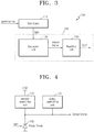
- FIG. 3 is a diagram illustrating a detector cell 100 included in a photomultiplier for tomography, according to example embodiments.
- the detector cell 100 of a photomultiplier for tomography may include a detector unit 130, and a readOUT unit 150.
- the detector unit 130 may be configured to receive light from the scintillator 110.
- the scintillator 110 may be arranged to generate photons for delivering light to detector units 130 in a plurality of detector cells 100.
- the photomultiplier may include pixel elements including at least 500 microcells, each of which has a size of about 20 ⁇ m. Each microcell independently detects and amplifies photons.
- the photomultiplier may be a silicon device, such as a photomultiplier ("SiPM"), but example embodiments are not limited thereto and other materials for the photomultiplier may be suitable.
- SiPM photomultiplier
- an output signal of the SiPM may be a signal obtained by summing the signals of all the microcells.
- the scintillator 110 receives radiation to generate photons. That is, a radioactive isotope (e.g., F-18-FDG) introduced into a patient or an object experiences a radioactive decay event.
- the radioactive decay event involves generation of positrons.
- the positrons generated by the radioactive decay event interact with the surrounding electrons, thereby causing an electron-positron annihilation event.
- the electron-positron annihilation event produces two oppositely directed radiation beams having an energy of 511 keV.
- the radiation beams travel at the speed of light. When these radiation beams collide with the scintillator 110, light (or photons) is (are) emitted.
- the scintillator 110 may be visible light.
- the light emitted from the scintillator 110 may be visible light having a wavelength of about 400 nm to about 450 nm.
- the scintillator 110 may be made of lutetium oxyorthosilicate (LSO), lutetium yttrium oxyorthosilicate (LYSO), mixed lutetium silicate (MLS), lutetium gadolinium oxyorthosilicate (LGSO), lanthanum bromide (LaBr), or a combination thereof.
- LSO lutetium oxyorthosilicate
- LYSO lutetium yttrium oxyorthosilicate
- MLS mixed lutetium silicate
- LGSO lutetium gadolinium oxyorthosilicate
- LaBr lanthanum bromide
- the material of the scintillator 110 is not limited thereto and other scintillator materials may also be used.
- the detector unit 130 receives the photon emitted from the scintillator 110 to generate a detect signal.
- the detect signal may be a digitized electrical signal.
- the detection signal may have a first digital value when the detector unit 130 does not receive light and have a second digital value when the detector unit 130 receives light.
- the detector unit 130 may be configured so the detect signal undergoes a transition from a first voltage level to a second voltage level in response to the reception of light (e.g., visible light) from the scintillator 110, and the detector unit 130 may be configured to the detect signal undergoes a transition from the second voltage level to the first voltage level when the reception of light from the scintillator 110 is stopped, where the first and second voltage levels are different.
- the detector unit 130 may include a photo diode. The photo diode receives light to generate an electrical signal.
- the electrical signal is an analogue signal, which may be converted to a digital signal after having undergone passive and active quenching and active reset processes.
- the material of the scintillator 110 in FIG. 3 may be selected for a gamma-ray detection application, example embodiments are not limited thereto. In different imaging applications, a different material for the scintillator may be used.
- the material of the scintillator 110 may be Csl for configuring the scintillator 110 to convert X-ray radiation into visible light that may be converted by the detector unit 130 into the detect signal.
- FIG. 4 is a diagram illustrating elements of a detector unit 130, according to example embodiments.
- the detector unit 130 may include a photo diode 133, a passive quenching unit 131, and an active quenching unit 135.
- the photo diode 133 may generate a current based on photons emitted from the scintillator 110.
- the detector unit 130 may include a plurality of photo diodes 133, and each photo diode 133 may be included in each of a plurality of cells.
- the photo diode 133 may be an avalanche photo diode.
- a supply voltage VDD that is applied may be a little lower than an operating voltage (e.g., breakdown voltage when an avalanche photo diode is used as the photo diode 133) of the photo diode 133. In this case, when the photo diode 133 receives the photons, the operating voltage thereof becomes equal to or less than the supply voltage VDD. Therefore, a current flows in the photo diode 133.
- the photo diode 133 may include two terminals, for example an anode and a cathode.
- the passive quenching unit 131 may be connected to the cathode of the photo diode 133.
- the passive quenching unit 131 generates a voltage difference between both terminals thereof in a state where a current flows in the photo diode 133.
- the passive quenching unit 131 may include, for example, a resistor and an equivalent circuit.
- a voltage drop generated by the passive quenching unit 131 reduces a voltage applied to the photo diode 133.
- the passive quenching unit 131 is an equivalent circuit and a resistor, the higher the intensity of the current flowing in the photo diode 133, the higher a voltage drop occurring in the passive quenching unit 131. Therefore, as the intensity of the current that flows in the photo diode 133 increases, the intensity of the voltage applied to the photo diode 133 decreases.
- the active quenching unit 135 shortens a time taken to stop current from flowing again, which is performed by the passive quenching unit 131. That is, if the passive quenching unit 131 maintains a voltage between both terminals of the photo diode 133 as an operating voltage of the photo diode 133, the active quenching unit 135 shortens a time taken for the voltage between both terminals of the photo diode 133 to change from the supply voltage VDD to the operating voltage of the photo diode 133. As a result, a recovery time of the photo diode 133 may be shortened, and resolution of the detector unit 130 may be increased.
- the detector unit 130 operates as follows.
- the photo diode 133 produces a current based on photons received by the scintillator 110.
- the voltage between both terminals of the photo diode 133 is set by the passive quenching unit 131 to be an operating voltage level of the photo diode 133, and the active quenching unit 133 shortens the time taken to change the voltage of the photo diode 133.
- the readOUT unit 150 receives a detect signal to generate an output signal OUT.
- the output signal OUT is not stored in a buffer or a separate memory, but is generated correspondingly to the detect signal.
- the readOUT 150 unit and detector cell 100 may be configured so as to not store the detect signal and/or the output signal.
- the output signal OUT is transmitted to an external circuit of the detector cell 100 of a photomultiplier.
- the external circuit may include an accumulator illustrated in FIG. 8 .
- an operation of a detector cell 100 included in a photomultiplier, according to example embodiments, will be described.
- a radioactive isotope that has been introduced into a patient or an object generates a gamma-ray through a radioactive decay event.
- the scintillator 110 receives the gamma-ray and emits photons.
- the detector unit 130 receives the photons emitted from the scintillator 110 to generate a detect signal.
- the readOUT unit 150 receives the detect signal generated by the detector unit 130 to generate an output signal OUT in the form of a signal format that an external circuit can receive, without separately storing or counting the detect signal.
- the output signal OUT is transmitted to the external circuit.
- a photomultiplier does not store the detect signal in the detector cell 100 (or a microcell). Right after receiving the detect signal, the readOUT unit generates the output signal OUT, which is then transmitted to the external circuit. Therefore, a space for an internal memory or a buffer is not needed, the size of a chip may be reduced, and integration may be obtained.
- the photomultiplier may increase a fill factor.
- the fill factor denotes an area ratio of a detecting part to a detector cell. For example, the fill factor may be increased up to 65% or more.
- an energy resolution of the detector cell 100 does not depend on the capacity of an internal memory or a buffer, but depends on the capacity of a memory of the external circuit, and thus, a detector cell with high energy resolution may be obtained.
- the photomultiplier may have a full width at half maximum (FWHM), which denotes an energy resolution of 10% or less.
- an energy dynamic range may be obtained by multiplying the number of the detector cells 100 (or microcells) by the capacity of a memory for storing the detect signal generated by the detector cell 100.
- the energy resolution of the detector cell 100 does not depend on the capacity of an internal memory, but instead may depend on the capacity of an external memory.
- the capacity of internal memory may be restricted by the size of the detector cell 100, while the capacity of the external memory may be relatively large. Therefore, the energy dynamic range increases in proportion to the capacity of the external memory.
- FIG. 5A is a diagram illustrating elements of a detector unit 130a, according to example embodiments.
- the detector unit 130a includes a photo diode 133a, a passive quenching unit 131a, an active quenching unit 135a, wherein the passive quenching unit 131a includes a capacitor CAP (capacitor or equivalent circuit).
- a voltage stored in the capacitor CAP (capacitor or equivalent circuit) of the passive quenching unit 131a may be controlled according to a temperature, processes, and other factors (e.g. environmental change). Therefore, although an operating voltage of the photo diode 133a varies according to temperatures, processes, and other factors (environmental change), a quenching operation may be performed.
- FIG. 5B is a characteristic curve of a photo diode, which is illustrated for explaining a method of controlling a passive quenching unit 131a of the detector unit of FIG. 5A , according to example embodiments.
- a voltage applied between both terminals of the photo diode 133 may vary according to temperatures, processes, and other factors (environmental change). For example, if the operating voltage of the photo diode 133 is represented as Vb, the voltage applied between both terminals of the photo diode 133 may be increased to Vb+a, according to temperatures, processes, and other environmental changes. In this case, a small amount of current flows in the photo diode 133, and thus, a circuit of the detector unit 130a may not operate. Thus, a voltage applied to the capacitor CAP increases so that the voltage applied between both terminals of the photo diode 133 is set to be Vb, whereby the circuit of the detector unit 130a may normally operate.
- the voltage applied between both terminals of the photo diode 133 may be decreased to Vb-a, according to temperatures, processes, and other factors (environmental change). In this case, an excessively large current flows in the photo diode 133, and thus, the circuit of the detector unit 130a may malfunction due to the overcurrent. Thus, the voltage applied to the capacitive element CAP is reduced so that the voltage applied between both terminals of the photo diode 133 is controlled to be equal to Vb, whereby the circuit of the detector unit 130a may normally operate.
- FIG. 6A is a diagram illustrating elements of a detector unit 130b, according to example embodiments.
- the detector unit 130b includes a photo diode 133b, a passive quenching unit 131b, an active quenching unit 135b, and an active reset unit 137.
- the active reset unit 137 shortens a time taken to restore the voltage between both terminals of the photo diode 133b to the supply voltage VDD. Therefore, when the subsequent photons are received, this enables the detection of the photons. That is, if the restoration time lengthens, the first received photons are difficult to distinguish from the subsequently received photons, and thus, this may be regarded as one-time reception of photons, resulting in low energy resolution. Therefore, the detector unit 130b includes the active reset unit 137, thereby shortening the restoration time and increasing the energy resolution.
- FIG. 6B is a circuit diagram of a detector unit 130b, according to example embodiments.
- the active quenching unit 135b may include a switch transistor SW2.
- the active reset unit 137 may include a switch transistor SW1.
- the passive quenching unit 133b may include a capacitor CAP_1.
- FIG. 6C is a timing graph showing a voltage between both terminals of a photo diode of the detector unit 130b of FIG. 6B according to time, according to example embodiments.
- a photo diode when a photo diode receives photons at a time t1, current flows in a node A, and a voltage between both terminals of the photo diode decreases. That is, a voltage of the node A decreases so that a logic LOW is applied to the node A. In other words, passive quenching occurs.
- a switch SW3 is switched on to apply a supply voltage VDD to a node B so that the node B enters a logic high state, and the switch transistor SW2 and a switch SW4 are in an ON state. Therefore, the voltage of the node A at a time period from t2 to t3 rapidly decreases. That is, active quenching occurs.
- the switch SW4 is switched on so that a voltage of a node C decreases, and thus, the node C enters a low state. Accordingly, the switch transistor SW1 is switched on. Therefore, the voltage of the node A at a time period from t3 to t4 maintains equilibrium. Since the node C enters a low state, a voltage of a node D enters a high state. In this regard, since the node C enters a low state, a time taken for the node D to enter a high state may be controlled by a switch SW6 and a capacitor CAP_2.
- the node C enters a low state, and after a certain period of time a switch SW5 is switched on so that a voltage of a node B enters a low state.
- the switch transistor SW2 is switched off, and a voltage of the node A at a time period from t4 to t5 is restored to the voltage VDD. That is, an active reset occurs.
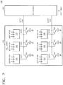
- FIG. 7 is a diagram illustrating a radiation detecting system 400 that includes an accumulator 300 and a cell array 200 including photomultiplier detector cells 101, 102, 103, 104, 105 and 106 for tomography, according to example embodiments.
- the cell array 200 may be included in a radiation detecting module or a pixel element, and may also indicate a plurality of detector cells.
- the radiation detecting system 400 includes the cell array 200 and the accumulator 300.
- the cell array 200 includes the photomultiplier detector cells 101, 102, 103, 104, 105 and 106 for tomography.
- Each of the photomultiplier detector cells 101, 102, 103, 104, 105 and 106 has a similar structure to that of the photomultiplier detector cell 100 illustrated in FIG. 3 .
- each of the photomultiplier detector cells 101, 102, 103, 104, 105 and 106 may include a detector unit and a readOUT unit, and be connected to a scintillator.
- FIG. 1 the photomultiplier detector cells 101, 102, 103, 104, 105 and 106 for tomography.
- FIG. 7 only 6 detector cells included in the cell array 200 are illustrated for convenience of explanation, but example embodiments are not limited thereto and the number of the detector cells is may be more or fewer than 6 detectors cells.
- FIG. 7 it is illustrated in FIG. 7 that 3 detector cells are connected to a single data line, but the number of the detector cells that are connected to a single data line is not limited thereto.
- 2 data lines are illustrated in FIG. 7 for convenience of explanation, but the number of the data lines is provided only for illustrative purposes and is not intended to limit the scope of example embodiments.
- the photomultiplier detector cells 101, 102, 103, 104, 105 and 106 each generate output signals OUT1, OUT2, OUT3, OUT4, OUT5 and OUT6, respectively, which are in the form of a signal format that the accumulator 300 can receive, without separately storing or counting the detect signals.
- the output signals OUT1, OUT2, OUT3, OUT4, OUT5 and OUT6 turn on or turn off switching circuits TR1, TR2, TR3, TR4, TR5 and TR6, respectively.
- the switching circuit TR1, TR2, TR3, TR4, TR5 and TR6 is respectively turned on or turned off, the amount of current that flows in a first data line DATA line1 and a second data line DATA line2 varies.
- the current flowing in the data lines is transmitted to the accumulator 300.
- the accumulator 300 receives the current flowing in the data lines to count or store the amount of detected radiation (e.g., gamma-ray).
- a space for an internal memory or a buffer in the cell array 200 is not needed, the size of a chip may be reduced, and integration may be obtained.
- energy resolution of each of the detector cells 101, 102, 103, 104, 105 and 106 does not depend on the capacity of an internal memory or a buffer, but depends on the capacity of a memory of the accumulator 300 which may have a relatively high capacity, and thus, high resolution detecting may be performed.
- FIG. 8 is a diagram illustrating a radiation detecting system 400a that includes an accumulator 300a and a cell array 200a including photomultiplier detector cells 101a, 102a, 103a, 104a, 105a and 106a for tomography, according to example embodiments.
- the radiation detecting system 400a includes the cell array 200a and the accumulator 300a.
- the cell array 200a includes the photomultiplier detector cells 101a, 102a, 103a, 104a, 105a and 106a for tomography.
- the cell array 200a has a similar structure to that of the cell array 200 of FIG. 7 .
- the number of detector cells of the cell array 200a, the number of detector cells that are connected to a single data line, and the number of the data lines are provided only for illustrative purposes and are not intended to limit the scope of example embodiments.
- the accumulator 300a includes a count unit 310a.
- the count unit 310a counts the number of cells that receive radiation.
- the count unit 310a generates a count signal which indicates the number of counted cells.
- the count unit 310a may include a plurality of sub-counters (refer to FIG. 9 ). Each sub-counter may count the number of cells that receive radiation and are connected to a single data line.
- the count unit 310a may combine sub-counter signals generated by the plurality of sub-counters to generate a count signal.
- the accumulator 300a receives current from the cell array 200a through first and second data lines DATA line1 and DATA line2.
- Switches TR1, TR2 and TR3 are turned on or turned off by output signals OUT1, OUT2 and OUT3 that are output from photomultiplier detector cells 101a, 102a and 103a.
- the switches TR1, TR2 and TR3 are turned on, current flows in the first data line DATA line1 according to the number of detector cells by which radiation (e.g., gamma-rays) is detected.
- a current I flows in the first data line DATA line1. If the current I flows in the first data line DATA line1, the current I may also flow in switches TR_x, TR_y and TR_z of the accumulator 300a through a current mirror. In this case, a first data D1 may enter a high state, and a second data D2 and a third data D3 may enter a low state.
- the switches TR1 and TR2 are turned on so that a current 2I (i.e., a current that is double the current I) flows in the first data line DATA line1. If the current 2I flows in the first data line DATA line1, a current 4I (i.e., a current that is four times greater than the current I) may flow in the switches TR_x, TR_y and TR_z of the accumulator 300a through a current mirror. In this case, the first data D1 and the second data D2 may enter a high state, and the third data D3 may enter a low state.
- a current 2I i.e., a current that is double the current I
- a current 4I i.e., a current that is four times greater than the current I
- a current 3I (i.e., a current that is three times greater than the current I) flows in the first data line DATA line1.
- the first data D1, the second data D2, and the third data D3 may enter a high state.
- FIG. 9 is a diagram illustrating a sub-counter 311a included in the count unit 310a of FIG. 8 , according to example embodiments.
- the sub-counter 311a receives a first data D1, a second data D2, and a third data D3 to output them as a sub-count signal.
- the sub-counter 311a receives the first and second data D1 and D2 and performs an XOR operation thereon.
- An XOR operation is performed on the value obtained as a result of the XOR operation and the third data D3 to generate a signal XOR-OUT.
- the signal XOR-OUT is input to a count circuit.
- the count circuit receives the signal XOR-OUT to output it as the sub-count signal.
- a count signal may be generated by performing a logical operation on sub-count signals that differ from a sub-count signal 1.
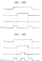
- FIGS. 10A through 10C are timing graphs each illustrating first, second and third data D1, D2 and D3 and a signal XOR-OUT according to a current that flows in a first data line DATA line1, according to example embodiments.
- FIG. 10A illustrates a timing graph of the first, second and third data D1, D2 and D3 and the signal XOR-OUT when the first D1 is in a high state and the second data D2 and the third data D3 are in a low state.
- FIG. 10B illustrates a timing graph of the first, second and third data D1, D2 and D3 and the signal XOR-OUT when the first data D1 and the second data D2 are in a high state and the third data D3 is in a low state.
- FIG. 10C illustrates a timing graph of the first, second and third data D1, D2 and D3 and the signal XOR-OUT when the first data D1, the second data D2, and the third data D3 are in a high state.
- a sub-count signal 1 may be a signal representing 1.
- the signal XOR-OUT is the same as illustrated in FIG. 10B .
- the count circuit may count a rising edge or a falling edge of the signal XOR-OUT. Therefore, the sub-count signal 1 may be a signal representing 2.
- the signal XOR-OUT is the same as illustrated in FIG. 10C .
- the count circuit may count a rising edge or a falling edge of the signal XOR-OUT. Therefore, the sub-count signal 1 may be a signal representing 3.
- the radiation detecting system 400a of FIG. 8 There are detector cells that detect radiation and detector cells that do not detect radiation in the photomultiplier detector cells 101a, 102a, 103a, 104a, 105a and 106a included in the cell array 200a.
- the number of the detector cells that detect radiation may increase in proportion to the density of radiation.
- the detector cells that detect radiation output whether or not the radiation is detected through the output signals OUT1, OUT2, OUT3, OUT4, OUT5 and OUT6.
- the output signals OUT1, OUT2, OUT3, OUT4, OUT5 and OUT6 turn on or turn off the switches TR1, TR2, TR3, TR4, TR5 and TR6.
- the switch in an ON state enables current to flow through the first data line DATA line1 or the second data line DATA line2.
- the first, second and third data D1, D2 and D3 are turned on or turned off to be input to the count unit 310a.
- a case of the second data line DATA line2 is similar to that of the first data line DATA line1.
- the count unit 310a performs a calculation based on the first to sixth data D1 to D6 to obtain a count signal, which indicates the number of counted detector cells, and then outputs the count signal. Therefore, photons that are consecutively incident or almost simultaneously incident may be detected through these processes.
- FIG. 11 is a diagram illustrating a radiation detecting system 400b that includes an accumulator 300b and a cell array 200b including photomultiplier detector cells 101b, 102b, 103b, 104b, 105b and 106b for tomography, according to example embodiments.
- the radiation detecting system 400b includes the cell array 200b and the accumulator 300b.
- the cell array 200b includes the photomultiplier detector cells 101b, 102b, 103b, 104b, 105b and 106b for tomography.
- the cell array 200b has a similar structure to that of the cell array 200 of FIG. 7 .
- the number of detector cells of the cell array 200b, the number of detector cells that are connected to a single data line, and the number of the data lines are provided only for illustrative purposes and are not intended to limit the scope of example embodiments.
- the accumulator 300b includes a count unit 310b.
- the count unit 310b counts the number of detector cells that receive radiation.
- the count unit 310b generates a count signal that indicates the number of counted detector cells.
- the count unit 310b may include a plurality of sub-counters. Each sub-counter may count the number of detector cells that are connected to a single data line and receive radiation.
- the count unit 310b may generate a count signal by combining sub-counter signals generated by the plurality of sub-counters.
- the accumulator 300b receives current from the cell array 200b through first and second data lines DATA line1 and DATA line2.
- Switches TR1, TR2 and TR3 are turned on or turned off by output signals OUT1, OUT2 and OUT3, respectively, which are output from the photomultiplier detector cells 101b, 102b and 103b, respectively.
- a current corresponding to the data line flows according to the number of detector cells by which radiation is detected. For example, if radiation is detected only in the photomultiplier detector cell 101b and not detected in the photomultiplier detector cells 102b and 103b, only the switch TR1 is turned on so that a current I flows in the first data line DATA line1.
- a current 3I (i.e., a current that is three times greater than the current I) flows in the first data line DATA line1.
- V_count1 R ⁇ I if the number of detector cells that detect radiation is 1
- V_count1 R ⁇ 2I if the number of detector cells that detect radiation is 2
- V_count1 R ⁇ 3I if the number of detector cells that detect radiation is 3. Therefore, the count unit 310b may detect the density of radiation according to the intensity of voltage. Accordingly, the count unit 310b generates the count signal.
- V_count2 denotes a value obtained by multiplying a resistance R by a current I (or 2I or 31), depending on the number of detector cells 104b, 105b, and 106b, that detect radiation.
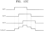
- FIGS. 12A through 12C are timing graphs each illustrating output signals OUT1, OUT2 and OUT3 and a count voltage V_count according to current that flows in a first data line DATA line1, according to example embodiments.
- FIG. 12A illustrates a timing graph of the output signals OUT1, OUT2 and OUT3 and the count voltage V_count when the switch TR1 is turned on and the switches TR2 and TR3 are turned off.
- FIG. 12B illustrates a timing graph of the output signals OUT1, OUT2 and OUT3 and the count voltage V_count when the switches TR1 and TR2 are turned on and the switch TR3 is turned off.
- FIG. 12C illustrates a timing graph of the output signals OUT1, OUT2 and OUT3 and the count voltage V_count when the switches TR1, TR2 and TR3 are turned on.
- the timing graph of FIG. 12A illustrates a case where radiation is detected in the photomultiplier detector cell 101b and is not detected in the photomultiplier detector cells 102b and 103b.
- the switch TR1 is turned on by the output signal OUT1
- the switch TR2 is turned on by the output signal OUT2
- the switch TR3 is turned on by the output signal OUT3.
- the current I flows in the first data line DATA line1 and the current I also flows in the switch TR_i. Therefore, the count voltage V_count1 may be represented as R ⁇ I.
- the count unit 310b may measure the density of the radiation by using the number of rising edges or the intensity of a maximum voltage.
- the timing graph of FIG. 12B illustrates a case where radiation is detected in the photomultiplier detector cells 101b and 102b and is not detected in the photomultiplier detector cell 103b.
- the switch TR1 is turned on by the output signal OUT1
- the switch TR2 is turned on by the output signal OUT2
- the switch TR3 is turned off by the output signal OUT3.
- the current 2I flows in the first data line DATA line1 and the current 2I also flows in the switch TR_i. Therefore, the count voltage V_count1 may be represented as R ⁇ 2I.
- the count voltage V_count1 may increase stepwise. Therefore, the count unit 310b may count the number of rising edges and measure the density of the radiation by using the intensity of a maximum voltage.
- the timing graph of FIG. 12C illustrates a case where radiation is detected in the photomultiplier detector cells 101b, 102b and 103b.
- the switch TR1 is turned on by the output signal OUT1
- the switch TR2 is turned on by the output signal OUT2
- the switch TR3 is turned on by the output signal OUT3.
- the current 3I flows in the first data line DATA line1 and also flows in the switch TR_i. Therefore, the count voltage V_count1 may be represented as R ⁇ 31.
- the count voltage V_count1 may increase stepwise. Therefore, the count unit 310b may count the number of rising edges and measure the density of the radiation by using the intensity of a maximum voltage.
- the first data line DATA line1 changes the count voltage V_count1 according to the number of detector cells that detect radiation.
- V_count1 R ⁇ I if the number of detector cells that detect radiation is 1
- V_count1 R ⁇ 2I if the number of detector cells that detect radiation is 2
- V_count1 R ⁇ 3I if the number of detector cells that detect radiation is 3.
- the count unit 310b performs a calculation based on the intensity of the count voltage V_count1, which indicates the number of counted detector cells that detect radiation, to obtain a count signal and output the count signal. Therefore, photons that are consecutively incident or almost simultaneously incident may be detected through these processes.
- a method of operating a radiation detecting system may include exposing a radiation-emitting source to a cell array that includes a scintillator and a switching circuit connected to a plurality of photomultiplier detector cells.
- the scintillator may be configured to generate light having a certain range of wavelength (e.g., visible light) based on radiation received from the radiation-emitting source (e.g., gamma-ray radiation).
- Each of the plurality of photomultiplier detector cells may include a detector unit that is configured to generate a digitized detect signal in response to receiving the light, and a readOUT unit that is configured to generate an output signal after receiving the digitized detect signal and to transmit the output signal to the switching circuit right after receiving the digitized detect signal.
- the method may further include transmitting a current signal from the switching circuit to an accumulator that is located outside of the cell array, where the current signal may correspond to a number of the plurality of photomultiplier detector cells detecting light.
- FIGS. 4 , 5A , 6A , 6B illustrate detector units 130, 130a, and 130b that include Photo Diodes 133, 133a, and 133b, respectively
- example embodiments are not limited thereto.
- a detector unit may alternatively include a different light-sensing element (e.g., light sensor transistor) having at least two terminals instead of one of the Photo Diodes 133, 133a, and 133b for generating a current based on photons emitted from the scintillator.
- a light-sensing element e.g., light sensor transistor
Landscapes
- Physics & Mathematics (AREA)
- Health & Medical Sciences (AREA)
- Life Sciences & Earth Sciences (AREA)
- General Physics & Mathematics (AREA)
- Spectroscopy & Molecular Physics (AREA)
- High Energy & Nuclear Physics (AREA)
- Molecular Biology (AREA)
- Engineering & Computer Science (AREA)
- Medical Informatics (AREA)
- Nuclear Medicine, Radiotherapy & Molecular Imaging (AREA)
- Biomedical Technology (AREA)
- Signal Processing (AREA)
- Multimedia (AREA)
- Optics & Photonics (AREA)
- Pathology (AREA)
- Radiology & Medical Imaging (AREA)
- Biophysics (AREA)
- Heart & Thoracic Surgery (AREA)
- Surgery (AREA)
- Animal Behavior & Ethology (AREA)
- General Health & Medical Sciences (AREA)
- Public Health (AREA)
- Veterinary Medicine (AREA)
- Measurement Of Radiation (AREA)
- Investigating Or Analysing Materials By Optical Means (AREA)
Description
- Example embodiments relate to a radiation detecting system for tomography.
- Methods of imaging the inside of the human body include positron emission tomography (PET), magnetic resonance tomography (MRI), X-ray computed tomography (CT), and the like. PET is one of the nuclear medicine diagnosis methods by which physiological and pathological images of human bodies are obtained by detecting emitted positrons by using a radioactive tracer substance. A diagnosis method by PET is performed such that a radioactive isotope, e.g., F-18-FDG (an analogue of glucose), is introduced into the human body, and radiation emitted as a result of cancer cells inside the body absorbing the radioactive isotope is detected after a certain period of time (e.g., tens of minutes), thereby obtaining position information of the cancer. Detectors for detecting radiation emitted as a result of cancer cells inside the body absorbing a radioactive isotope are referred to as silicon photomultiplier detectors or gamma-ray detectors. In addition, apparatuses for detecting radiation or gamma-rays may be used in radiation detectors used for single photon emission computed tomography (SPECT) or computed tomography and in various applications such as astronomy and space science.
- Tisa S et al. present a fully-integrated CMOS implementation of a sensor chip that contains a Single-Photon Avalanche Diode (SPAD) in a paper entitled "On-chip detection and counting of single-photons" (INTERNATIONAL ELECTRON DEVICES MEETING 5-7.12.2005, IEEE, IEEE, PISCATAWAY, NJ. USA, 5 December 2005 (2005-12-05), pages 815-818. ISBN: 978-0-7803-9268-7).
- German Patent Application Publication Number
DE 102010041805 A1 relates to a device having a plurality of photosensitive microcells arranged in row or matrix form. Pozas-Flores F et al. present the design in CMOS of an array of detector cells in a paper entitled "Design of a smart SiPM based on focal-plane processing elements for improved spatial resolution in PET" (BIOELECTRONICS, BIOMEDICAL, AND BIOINSPIRED SYSTEMS V; AND NANOTECHNOLOGY V, SPIE, 1000 20TH ST. BELLINGHAM WA 98225-6705 USA, vol. 8068, no. 1,4 May 2011). - The invention is defined by the claims.
- Example embodiments relate to photomultiplier detector cells that are configured to collect image material in a constant surface area at a relatively high density. Additional aspects will be set forth in part in the description which follows and, in part, will be apparent from the description, or may be learned by practice of example embodiments.
- These and/or other aspects will become apparent and more readily appreciated from the following description of non-limiting embodiments, as illustrated in the accompanying drawings in which like reference characters refer to the same parts throughout the different views. The drawings are not necessarily to scale, emphasis instead being placed upon illustrating the principles of example embodiments. In the drawings:
-
FIG. 1 is a schematic diagram illustrating a radiation measuring device, according to example embodiments; -
FIG. 2 is a schematic cross-sectional view of a radiation detecting module, according to example embodiments; -
FIG. 3 is a diagram illustrating a detector cell included in a photomultiplier for tomography, according to example embodiments; -
FIG. 4 is a diagram illustrating elements of a detector unit, according to example embodiments; -
FIG. 5A is a diagram illustrating elements of a detector unit, according to example embodiments; -
FIG. 5B is a characteristic curve of a photo diode, which is illustrated for explaining a method of controlling a passive quenching unit of the detector unit ofFIG. 5A , according to example embodiments; -
FIG. 6A is a diagram illustrating elements of a detector unit, according to example embodiments; -
FIG. 6B is a circuit diagram of a detector unit, according to example embodiments; -
FIG. 6C is a timing graph showing a voltage between both terminals of a photo diode of the detector unit ofFIG. 6B according to time, according to example embodiments; -
FIG. 7 is a diagram illustrating a radiation detecting system that includes an accumulator and a cell array including photomultiplier detector cells for tomography, according to example embodiments; -
FIG. 8 is a diagram illustrating a radiation detecting system that includes an accumulator and a cell array including photomultiplier detector cells for tomography, according to example embodiments; -
FIG. 9 is a diagram illustrating a sub-counter included in a count unit, according to example embodiments; -
FIGS. 10A through 10C are timing graphs each illustrating data and a signal according to current that flows in a data line, according to example embodiments; -
FIG. 11 is a diagram illustrating a radiation detecting system that includes an accumulator and a cell array including photomultiplier detector cells for tomography, according to example embodiments; and -
FIGS. 12A through 12C are timing graphs each illustrating output signals and a count voltage according to current that flows in a data line, according to example embodiments. - Example embodiments will now be described more fully with reference to the accompanying drawings, in which some example embodiments are shown. Example embodiments, may however, be embodied in many different forms and should not be construed as being limited to embodiments set forth herein. Rather, these example embodiments are provided so that this disclosure will be thorough and complete, and will fully convey the scope of example embodiments to one of ordinary skill in the art. In the drawings, the thicknesses of layers and regions are exaggerated for clarity. Like reference numerals in the drawings denote like elements, and thus their description may be omitted.
- The terminology used herein is for the purpose of describing particular embodiments only and is not intended to be limiting of example embodiments. As used herein, the singular forms are intended to include the plural forms as well, unless the context clearly indicates otherwise. It will be further understood that the terms "comprises" and/or "comprising," when used in this specification, specify the presence of stated features, integers, steps, operations, components, elements, and/or groups thereof, but do not preclude the presence or addition of one or more other features, integers, steps, operations, components, elements, and/or groups thereof. As used herein, the term "and/or" includes any and all combinations of one or more of the associated listed items. Expressions such as "at least one of," when preceding a list of elements, modify the entire list of elements and do not modify the individual elements of the list.
- It will be understood that, although the terms "first, second, etc." may be used herein to describe various elements, components, regions, layers, and/or sections, these elements, components, regions, layers, and/or sections should not be limited by these terms. These terms are only used to distinguish one element, component, region or section from another element, component, region or section. Thus, a first element, component, region or section discussed below could be termed a second element, component, region or section without departing from the teachings of example embodiments.
- Hereafter, example embodiments will be described with reference to the accompanying schematic drawings. In the drawings, variations from the shapes of the illustrations as a result, for example, of manufacturing techniques and/or tolerances, are to be expected. Thus, example embodiments should not be construed as limited to the particular shapes of regions illustrated herein but are to include deviations in shapes that result, for example, from manufacturing.
- Unless otherwise defined, all terms (including technical and scientific terms) used herein have the same meaning as commonly understood by one of ordinary skill in the art to which example embodiments belong. It will be further understood that terms, such as those defined in commonly-used dictionaries, should be interpreted as having a meaning that is consistent with their meaning in the context of the relevant art and will not be interpreted in an idealized or overly formal sense unless expressly so defined herein.
-
FIG. 1 is a schematic diagram illustrating aradiation measuring device 1, according to example embodiments. - As illustrated in
FIG. 1 , theradiation measuring device 1 may include a plurality ofradiation measuring modules 2, animaging processing unit 3, and animaging zone 4. - The
imaging zone 4, which is a zone for accommodating a target, is a zone provided to measure an image of the target. To support the target, theimaging zone 4 may include asupport 5. Theradiation measuring modules 2 may receive radiation from the target and convert the radiation to a detect signal. Eachradiation measuring module 2 may include a plurality of radiation detecting modules 20 (refer toFIG. 2 ). This feature will be described below in more detail. Theimaging processing unit 3 may produce an image of a target based on the detect signal generated by theradiation measuring module 2. -
FIG. 2 is a schematic cross-sectional view of aradiation detecting module 20, according to example embodiments. - As illustrated in
FIG. 2 , theradiation detecting module 20 may include ascintillator 21, anoptical pipe 22,pixel elements semiconductor chip 24. - The
scintillator 21 may receive radiation (e.g., gamma rays) to generate photons. Theoptical pipe 22 may be disposed between thescintillator 21 and thesemiconductor chip 24, and deliver the photons generated by thescintillator 21 to thesemiconductor chip 24. In this regard, an incident direction of the photons delivered to thesemiconductor chip 24 is not particularly limiting. For example, the photons may be incident from an upper portion of thescintillator 21 or incident through a lower portion of thesemiconductor chip 24. In this case, thesemiconductor chip 24 may be made of a material enabling photons to pass therethrough. - The
semiconductor chip 24 may include a plurality ofpixel elements semiconductor chip 24 receives the photons delivered through theoptical pipe 22 and produces an electrical signal corresponding to the photons. Each of thepixel elements detector cells 100 illustrated inFIG. 3 . For example, when each pixel element includes 16detector cells 100 and the pixel elements are arranged in thesemiconductor chip 24 in a 7 x 7 array configuration, thesemiconductor chip 24 may include 784 (7 x 7 x 16)detector cells 100. Thedetector cells 100 may be generally represented as microcells. If each microcell (e.g., detector cell 100) includes two photo diodes, thesemiconductor chip 24 may include 1,568 (7 x 7 x 16 x 2) photo diodes. -
FIG. 3 is a diagram illustrating adetector cell 100 included in a photomultiplier for tomography, according to example embodiments. - As illustrated in
FIG. 3 , thedetector cell 100 of a photomultiplier for tomography may include adetector unit 130, and areadOUT unit 150. Thedetector unit 130 may be configured to receive light from thescintillator 110. Thescintillator 110 may be arranged to generate photons for delivering light todetector units 130 in a plurality ofdetector cells 100. - The photomultiplier may include pixel elements including at least 500 microcells, each of which has a size of about 20 µm. Each microcell independently detects and amplifies photons. The photomultiplier may be a silicon device, such as a photomultiplier ("SiPM"), but example embodiments are not limited thereto and other materials for the photomultiplier may be suitable. When photons enter each microcell to generate an electron-hole pair, amplification occurs therein due to an electric field inside the SiPM, whereby each microcell generates and outputs a certain size of a signal. In this case, an output signal of the SiPM may be a signal obtained by summing the signals of all the microcells.
- The
scintillator 110 receives radiation to generate photons. That is, a radioactive isotope (e.g., F-18-FDG) introduced into a patient or an object experiences a radioactive decay event. The radioactive decay event involves generation of positrons. The positrons generated by the radioactive decay event interact with the surrounding electrons, thereby causing an electron-positron annihilation event. The electron-positron annihilation event produces two oppositely directed radiation beams having an energy of 511 keV. The radiation beams travel at the speed of light. When these radiation beams collide with thescintillator 110, light (or photons) is (are) emitted. In this case, light emitted from thescintillator 110 may be visible light. In particular, the light emitted from thescintillator 110 may be visible light having a wavelength of about 400 nm to about 450 nm. In this regard, thescintillator 110 may be made of lutetium oxyorthosilicate (LSO), lutetium yttrium oxyorthosilicate (LYSO), mixed lutetium silicate (MLS), lutetium gadolinium oxyorthosilicate (LGSO), lanthanum bromide (LaBr), or a combination thereof. However, the material of thescintillator 110 is not limited thereto and other scintillator materials may also be used. Thedetector unit 130 receives the photon emitted from thescintillator 110 to generate a detect signal. The detect signal may be a digitized electrical signal. For example, the detection signal may have a first digital value when thedetector unit 130 does not receive light and have a second digital value when thedetector unit 130 receives light. In other words, thedetector unit 130 may be configured so the detect signal undergoes a transition from a first voltage level to a second voltage level in response to the reception of light (e.g., visible light) from thescintillator 110, and thedetector unit 130 may be configured to the detect signal undergoes a transition from the second voltage level to the first voltage level when the reception of light from thescintillator 110 is stopped, where the first and second voltage levels are different. Thedetector unit 130 may include a photo diode. The photo diode receives light to generate an electrical signal. The electrical signal is an analogue signal, which may be converted to a digital signal after having undergone passive and active quenching and active reset processes. - Although the material of the
scintillator 110 inFIG. 3 may be selected for a gamma-ray detection application, example embodiments are not limited thereto. In different imaging applications, a different material for the scintillator may be used. For example, in X-ray detection, the material of thescintillator 110 may be Csl for configuring thescintillator 110 to convert X-ray radiation into visible light that may be converted by thedetector unit 130 into the detect signal. -
FIG. 4 is a diagram illustrating elements of adetector unit 130, according to example embodiments. - Referring to
FIG. 4 , thedetector unit 130 may include aphoto diode 133, a passive quenching unit 131, and anactive quenching unit 135. - The
photo diode 133 may generate a current based on photons emitted from thescintillator 110. Thedetector unit 130 may include a plurality ofphoto diodes 133, and eachphoto diode 133 may be included in each of a plurality of cells. For example, thephoto diode 133 may be an avalanche photo diode. A supply voltage VDD that is applied may be a little lower than an operating voltage (e.g., breakdown voltage when an avalanche photo diode is used as the photo diode 133) of thephoto diode 133. In this case, when thephoto diode 133 receives the photons, the operating voltage thereof becomes equal to or less than the supply voltage VDD. Therefore, a current flows in thephoto diode 133. - The
photo diode 133 may include two terminals, for example an anode and a cathode. The passive quenching unit 131 may be connected to the cathode of thephoto diode 133. - The passive quenching unit 131 generates a voltage difference between both terminals thereof in a state where a current flows in the
photo diode 133. The passive quenching unit 131 may include, for example, a resistor and an equivalent circuit. A voltage drop generated by the passive quenching unit 131 reduces a voltage applied to thephoto diode 133. For example, when the passive quenching unit 131 is an equivalent circuit and a resistor, the higher the intensity of the current flowing in thephoto diode 133, the higher a voltage drop occurring in the passive quenching unit 131. Therefore, as the intensity of the current that flows in thephoto diode 133 increases, the intensity of the voltage applied to thephoto diode 133 decreases. This is attributed to a constant supply voltage VDD. As a result, the intensity of the current that flows in thephoto diode 133 increases, and at some point a voltage that is lower than the operating voltage of thephoto diode 133 is applied on thephoto diode 133. Therefore, the flow of the current generated when thephoto diode 133 receives the photons is stopped by the passive quenching unit 131. - The
active quenching unit 135 shortens a time taken to stop current from flowing again, which is performed by the passive quenching unit 131. That is, if the passive quenching unit 131 maintains a voltage between both terminals of thephoto diode 133 as an operating voltage of thephoto diode 133, theactive quenching unit 135 shortens a time taken for the voltage between both terminals of thephoto diode 133 to change from the supply voltage VDD to the operating voltage of thephoto diode 133. As a result, a recovery time of thephoto diode 133 may be shortened, and resolution of thedetector unit 130 may be increased. - The
detector unit 130 operates as follows. Thephoto diode 133 produces a current based on photons received by thescintillator 110. In this regard, the voltage between both terminals of thephoto diode 133 is set by the passive quenching unit 131 to be an operating voltage level of thephoto diode 133, and theactive quenching unit 133 shortens the time taken to change the voltage of thephoto diode 133. - Referring back to
FIG. 3 , thereadOUT unit 150 receives a detect signal to generate an output signal OUT. According to example embodiments, the output signal OUT is not stored in a buffer or a separate memory, but is generated correspondingly to the detect signal. In other words, thereadOUT 150 unit anddetector cell 100 may be configured so as to not store the detect signal and/or the output signal. The output signal OUT is transmitted to an external circuit of thedetector cell 100 of a photomultiplier. The external circuit may include an accumulator illustrated inFIG. 8 . Hereinafter, an operation of adetector cell 100 included in a photomultiplier, according to example embodiments, will be described. A radioactive isotope that has been introduced into a patient or an object generates a gamma-ray through a radioactive decay event. Thescintillator 110 receives the gamma-ray and emits photons. Thedetector unit 130 receives the photons emitted from thescintillator 110 to generate a detect signal. ThereadOUT unit 150 receives the detect signal generated by thedetector unit 130 to generate an output signal OUT in the form of a signal format that an external circuit can receive, without separately storing or counting the detect signal. The output signal OUT is transmitted to the external circuit. - Therefore, a photomultiplier, according to example embodiments, does not store the detect signal in the detector cell 100 (or a microcell). Right after receiving the detect signal, the readOUT unit generates the output signal OUT, which is then transmitted to the external circuit. Therefore, a space for an internal memory or a buffer is not needed, the size of a chip may be reduced, and integration may be obtained. The photomultiplier may increase a fill factor. The fill factor denotes an area ratio of a detecting part to a detector cell. For example, the fill factor may be increased up to 65% or more.
- In addition, an energy resolution of the
detector cell 100 does not depend on the capacity of an internal memory or a buffer, but depends on the capacity of a memory of the external circuit, and thus, a detector cell with high energy resolution may be obtained. In particular, the photomultiplier may have a full width at half maximum (FWHM), which denotes an energy resolution of 10% or less. - In addition, an energy dynamic range may be obtained by multiplying the number of the detector cells 100 (or microcells) by the capacity of a memory for storing the detect signal generated by the
detector cell 100. The energy resolution of thedetector cell 100 does not depend on the capacity of an internal memory, but instead may depend on the capacity of an external memory. The capacity of internal memory may be restricted by the size of thedetector cell 100, while the capacity of the external memory may be relatively large. Therefore, the energy dynamic range increases in proportion to the capacity of the external memory. -
FIG. 5A is a diagram illustrating elements of adetector unit 130a, according to example embodiments. - Referring to
FIG. 5A , thedetector unit 130a includes aphoto diode 133a, apassive quenching unit 131a, anactive quenching unit 135a, wherein thepassive quenching unit 131a includes a capacitor CAP (capacitor or equivalent circuit). A voltage stored in the capacitor CAP (capacitor or equivalent circuit) of thepassive quenching unit 131a may be controlled according to a temperature, processes, and other factors (e.g. environmental change). Therefore, although an operating voltage of thephoto diode 133a varies according to temperatures, processes, and other factors (environmental change), a quenching operation may be performed. -
FIG. 5B is a characteristic curve of a photo diode, which is illustrated for explaining a method of controlling apassive quenching unit 131a of the detector unit ofFIG. 5A , according to example embodiments. - Referring to
FIG. 5B , a voltage applied between both terminals of thephoto diode 133 may vary according to temperatures, processes, and other factors (environmental change). For example, if the operating voltage of thephoto diode 133 is represented as Vb, the voltage applied between both terminals of thephoto diode 133 may be increased to Vb+a, according to temperatures, processes, and other environmental changes. In this case, a small amount of current flows in thephoto diode 133, and thus, a circuit of thedetector unit 130a may not operate. Thus, a voltage applied to the capacitor CAP increases so that the voltage applied between both terminals of thephoto diode 133 is set to be Vb, whereby the circuit of thedetector unit 130a may normally operate. Also, the voltage applied between both terminals of thephoto diode 133 may be decreased to Vb-a, according to temperatures, processes, and other factors (environmental change). In this case, an excessively large current flows in thephoto diode 133, and thus, the circuit of thedetector unit 130a may malfunction due to the overcurrent. Thus, the voltage applied to the capacitive element CAP is reduced so that the voltage applied between both terminals of thephoto diode 133 is controlled to be equal to Vb, whereby the circuit of thedetector unit 130a may normally operate. -
FIG. 6A is a diagram illustrating elements of adetector unit 130b, according to example embodiments. - Referring to
FIG. 6A , thedetector unit 130b includes aphoto diode 133b, apassive quenching unit 131b, anactive quenching unit 135b, and anactive reset unit 137. - If the
photo diode 133b stops receiving photons, a voltage between both terminals of thephoto diode 133b is restored to a supply voltage VDD. In this regard, theactive reset unit 137 shortens a time taken to restore the voltage between both terminals of thephoto diode 133b to the supply voltage VDD. Therefore, when the subsequent photons are received, this enables the detection of the photons. That is, if the restoration time lengthens, the first received photons are difficult to distinguish from the subsequently received photons, and thus, this may be regarded as one-time reception of photons, resulting in low energy resolution. Therefore, thedetector unit 130b includes theactive reset unit 137, thereby shortening the restoration time and increasing the energy resolution. -
FIG. 6B is a circuit diagram of adetector unit 130b, according to example embodiments. - Referring to
FIG. 6B , theactive quenching unit 135b may include a switch transistor SW2. Theactive reset unit 137 may include a switch transistor SW1. Thepassive quenching unit 133b may include a capacitor CAP_1. -
FIG. 6C is a timing graph showing a voltage between both terminals of a photo diode of thedetector unit 130b ofFIG. 6B according to time, according to example embodiments. - Referring to
FIGS. 6B and6C , when a photo diode receives photons at a time t1, current flows in a node A, and a voltage between both terminals of the photo diode decreases. That is, a voltage of the node A decreases so that a logic LOW is applied to the node A. In other words, passive quenching occurs. Thus, a switch SW3 is switched on to apply a supply voltage VDD to a node B so that the node B enters a logic high state, and the switch transistor SW2 and a switch SW4 are in an ON state. Therefore, the voltage of the node A at a time period from t2 to t3 rapidly decreases. That is, active quenching occurs. The switch SW4 is switched on so that a voltage of a node C decreases, and thus, the node C enters a low state. Accordingly, the switch transistor SW1 is switched on. Therefore, the voltage of the node A at a time period from t3 to t4 maintains equilibrium. Since the node C enters a low state, a voltage of a node D enters a high state. In this regard, since the node C enters a low state, a time taken for the node D to enter a high state may be controlled by a switch SW6 and a capacitor CAP_2. Therefore, the node C enters a low state, and after a certain period of time a switch SW5 is switched on so that a voltage of a node B enters a low state. As a result, the switch transistor SW2 is switched off, and a voltage of the node A at a time period from t4 to t5 is restored to the voltage VDD. That is, an active reset occurs. -
FIG. 7 is a diagram illustrating aradiation detecting system 400 that includes anaccumulator 300 and acell array 200 includingphotomultiplier detector cells cell array 200 may be included in a radiation detecting module or a pixel element, and may also indicate a plurality of detector cells. - Referring to
FIG. 7 , theradiation detecting system 400 includes thecell array 200 and theaccumulator 300. Thecell array 200 includes thephotomultiplier detector cells photomultiplier detector cells photomultiplier detector cell 100 illustrated inFIG. 3 . Thus, each of thephotomultiplier detector cells FIG. 7 , only 6 detector cells included in thecell array 200 are illustrated for convenience of explanation, but example embodiments are not limited thereto and the number of the detector cells is may be more or fewer than 6 detectors cells. In addition, for convenience of explanation, it is illustrated inFIG. 7 that 3 detector cells are connected to a single data line, but the number of the detector cells that are connected to a single data line is not limited thereto. In addition, 2 data lines are illustrated inFIG. 7 for convenience of explanation, but the number of the data lines is provided only for illustrative purposes and is not intended to limit the scope of example embodiments. - The
photomultiplier detector cells accumulator 300 can receive, without separately storing or counting the detect signals. The output signals OUT1, OUT2, OUT3, OUT4, OUT5 and OUT6 turn on or turn off switching circuits TR1, TR2, TR3, TR4, TR5 and TR6, respectively. When the switching circuit TR1, TR2, TR3, TR4, TR5 and TR6 is respectively turned on or turned off, the amount of current that flows in a first data line DATA line1 and a second data line DATA line2 varies. The current flowing in the data lines is transmitted to theaccumulator 300. Theaccumulator 300 receives the current flowing in the data lines to count or store the amount of detected radiation (e.g., gamma-ray). - Therefore, a space for an internal memory or a buffer in the
cell array 200 is not needed, the size of a chip may be reduced, and integration may be obtained. In addition, energy resolution of each of thedetector cells accumulator 300 which may have a relatively high capacity, and thus, high resolution detecting may be performed. -
FIG. 8 is a diagram illustrating aradiation detecting system 400a that includes anaccumulator 300a and acell array 200a includingphotomultiplier detector cells - Referring to
FIG. 8 , theradiation detecting system 400a includes thecell array 200a and theaccumulator 300a. Thecell array 200a includes thephotomultiplier detector cells cell array 200a has a similar structure to that of thecell array 200 ofFIG. 7 . Similarly as described above with respect to thecell array 200 ofFIG. 7 , the number of detector cells of thecell array 200a, the number of detector cells that are connected to a single data line, and the number of the data lines are provided only for illustrative purposes and are not intended to limit the scope of example embodiments. - The
accumulator 300a includes acount unit 310a. Thecount unit 310a counts the number of cells that receive radiation. Thecount unit 310a generates a count signal which indicates the number of counted cells. Thecount unit 310a may include a plurality of sub-counters (refer toFIG. 9 ). Each sub-counter may count the number of cells that receive radiation and are connected to a single data line. Thecount unit 310a may combine sub-counter signals generated by the plurality of sub-counters to generate a count signal. - Referring to
FIG. 8 , theaccumulator 300a receives current from thecell array 200a through first and second data lines DATA line1 and DATA line2. Switches TR1, TR2 and TR3 are turned on or turned off by output signals OUT1, OUT2 and OUT3 that are output fromphotomultiplier detector cells - For example, if radiation is detected only in the
photomultiplier detector cell 101 a and is not detected in thephotomultiplier detector cells accumulator 300a through a current mirror. In this case, a first data D1 may enter a high state, and a second data D2 and a third data D3 may enter a low state. - Alternatively, if radiation is detected in the
photomultiplier detector cells photomultiplier detector cell 103a, the switches TR1 and TR2 are turned on so that a current 2I (i.e., a current that is double the current I) flows in the first data line DATA line1. If the current 2I flows in the first data line DATA line1, a current 4I (i.e., a current that is four times greater than the current I) may flow in the switches TR_x, TR_y and TR_z of theaccumulator 300a through a current mirror. In this case, the first data D1 and the second data D2 may enter a high state, and the third data D3 may enter a low state. - Alternatively, if radiation is detected in the three
photomultiplier detector cells -
FIG. 9 is a diagram illustrating a sub-counter 311a included in thecount unit 310a ofFIG. 8 , according to example embodiments. The sub-counter 311a receives a first data D1, a second data D2, and a third data D3 to output them as a sub-count signal. In particular, the sub-counter 311a receives the first and second data D1 and D2 and performs an XOR operation thereon. An XOR operation is performed on the value obtained as a result of the XOR operation and the third data D3 to generate a signal XOR-OUT. The signal XOR-OUT is input to a count circuit. The count circuit receives the signal XOR-OUT to output it as the sub-count signal. A count signal may be generated by performing a logical operation on sub-count signals that differ from asub-count signal 1. -
FIGS. 10A through 10C are timing graphs each illustrating first, second and third data D1, D2 and D3 and a signal XOR-OUT according to a current that flows in a first data line DATA line1, according to example embodiments. In particular,FIG. 10A illustrates a timing graph of the first, second and third data D1, D2 and D3 and the signal XOR-OUT when the first D1 is in a high state and the second data D2 and the third data D3 are in a low state.FIG. 10B illustrates a timing graph of the first, second and third data D1, D2 and D3 and the signal XOR-OUT when the first data D1 and the second data D2 are in a high state and the third data D3 is in a low state.FIG. 10C illustrates a timing graph of the first, second and third data D1, D2 and D3 and the signal XOR-OUT when the first data D1, the second data D2, and the third data D3 are in a high state. - Referring to
FIGS. 8 ,7 , and10A , if the current I flows in the first data line DATA line1, the first data D1 may enter a high state and the second data D2 and the third data D3 may enter a low state. Thus, the signal XOR-OUT is the same as illustrated inFIG. 10A . The count circuit may count a rising edge or a falling edge of the signal XOR-OUT. Therefore, asub-count signal 1 may be a signal representing 1. Referring toFIGS. 7 ,8 , and10B , if the current 2I flows in the first data line DATA line1, the first data D1 and the second data D2 may enter a high state and the third data D3 may enter a low state. Thus, the signal XOR-OUT is the same as illustrated inFIG. 10B . The count circuit may count a rising edge or a falling edge of the signal XOR-OUT. Therefore, thesub-count signal 1 may be a signal representing 2. Referring toFIGS. 7 ,8 , and10C , if the current 3I flows in the first data line DATA line1, the first data D1, the second data D2, and the third data D3 may enter a high state. Thus, the signal XOR-OUT is the same as illustrated inFIG. 10C . The count circuit may count a rising edge or a falling edge of the signal XOR-OUT. Therefore, thesub-count signal 1 may be a signal representing 3. - Hereinafter, an operation of the
radiation detecting system 400a ofFIG. 8 will be described. There are detector cells that detect radiation and detector cells that do not detect radiation in thephotomultiplier detector cells cell array 200a. The number of the detector cells that detect radiation may increase in proportion to the density of radiation. The detector cells that detect radiation output whether or not the radiation is detected through the output signals OUT1, OUT2, OUT3, OUT4, OUT5 and OUT6. The output signals OUT1, OUT2, OUT3, OUT4, OUT5 and OUT6 turn on or turn off the switches TR1, TR2, TR3, TR4, TR5 and TR6. The switch in an ON state enables current to flow through the first data line DATA line1 or the second data line DATA line2. At this time, the first, second and third data D1, D2 and D3 are turned on or turned off to be input to thecount unit 310a. A case of the second data line DATA line2 is similar to that of the first data line DATA line1. Thecount unit 310a performs a calculation based on the first to sixth data D1 to D6 to obtain a count signal, which indicates the number of counted detector cells, and then outputs the count signal. Therefore, photons that are consecutively incident or almost simultaneously incident may be detected through these processes. -
FIG. 11 is a diagram illustrating aradiation detecting system 400b that includes anaccumulator 300b and acell array 200b includingphotomultiplier detector cells - Referring to
FIG. 11 , theradiation detecting system 400b includes thecell array 200b and theaccumulator 300b. Thecell array 200b includes thephotomultiplier detector cells cell array 200b has a similar structure to that of thecell array 200 ofFIG. 7 . Similarly as described above with respect to thecell array 200, in example embodiments, the number of detector cells of thecell array 200b, the number of detector cells that are connected to a single data line, and the number of the data lines are provided only for illustrative purposes and are not intended to limit the scope of example embodiments. - The
accumulator 300b includes acount unit 310b. Thecount unit 310b counts the number of detector cells that receive radiation. Thecount unit 310b generates a count signal that indicates the number of counted detector cells. Thecount unit 310b may include a plurality of sub-counters. Each sub-counter may count the number of detector cells that are connected to a single data line and receive radiation. Thecount unit 310b may generate a count signal by combining sub-counter signals generated by the plurality of sub-counters. - The
accumulator 300b receives current from thecell array 200b through first and second data lines DATA line1 and DATA line2. Switches TR1, TR2 and TR3 are turned on or turned off by output signals OUT1, OUT2 and OUT3, respectively, which are output from thephotomultiplier detector cells photomultiplier detector cell 101b and not detected in thephotomultiplier detector cells photomultiplier detector cells photomultiplier detector cell 103b, the switches TR1 and TR2 are turned on so that a current 2I flows in the first data line DATA line1. Similarly, if radiation is detected in thephotomultiplier detector cells - The
accumulator 300b includes thecount unit 310b. If the current I flows in the first data line DATA line1, the current I also flows in a switch Tr_i that is opposite to a current mirror. Therefore, V_count1 denotes a value obtained by multiplying a resistance R by a current I. That is, V_count1 = R × I. Similarly, if the current 2I flows in the first data line DATA line1, a current 4I flows in the switch Tr_i that is opposite to a current mirror. Therefore, V_count1 denotes a value obtained by multiplying a resistance R by the current 21. That is, V_count1 = R × 21. Similarly, if the current 3I flows in the first data line DATA line1, a current 5I flows in the switch Tr_i. Therefore, V_count1 denotes a value obtained by multiplying a resistance R and the current 31. That is, V_count1 = R × 3I. In other words, V_count1 = R × I if the number of detector cells that detect radiation is 1, V_count1 = R × 2I if the number of detector cells that detect radiation is 2, and V_count1 = R × 3I if the number of detector cells that detect radiation is 3. Therefore, thecount unit 310b may detect the density of radiation according to the intensity of voltage. Accordingly, thecount unit 310b generates the count signal. Similarly, if the current I flows in the second dataline DATA line 2, the current also flows in a switch Tr_j that is opposite to a current mirror. Similarly, V_count2 denotes a value obtained by multiplying a resistance R by a current I (or 2I or 31), depending on the number ofdetector cells -
FIGS. 12A through 12C are timing graphs each illustrating output signals OUT1, OUT2 and OUT3 and a count voltage V_count according to current that flows in a first data line DATA line1, according to example embodiments. In particular,FIG. 12A illustrates a timing graph of the output signals OUT1, OUT2 and OUT3 and the count voltage V_count when the switch TR1 is turned on and the switches TR2 and TR3 are turned off.FIG. 12B illustrates a timing graph of the output signals OUT1, OUT2 and OUT3 and the count voltage V_count when the switches TR1 and TR2 are turned on and the switch TR3 is turned off.FIG. 12C illustrates a timing graph of the output signals OUT1, OUT2 and OUT3 and the count voltage V_count when the switches TR1, TR2 and TR3 are turned on. - Referring to
FIGS. 11 and12A , the timing graph ofFIG. 12A illustrates a case where radiation is detected in thephotomultiplier detector cell 101b and is not detected in thephotomultiplier detector cells count unit 310b may measure the density of the radiation by using the number of rising edges or the intensity of a maximum voltage. - Referring to
FIGS. 11 and12B , the timing graph ofFIG. 12B illustrates a case where radiation is detected in thephotomultiplier detector cells photomultiplier detector cell 103b. The switch TR1 is turned on by the output signal OUT1, the switch TR2 is turned on by the output signal OUT2, and the switch TR3 is turned off by the output signal OUT3. Thus, the current 2I flows in the first data line DATA line1 and the current 2I also flows in the switch TR_i. Therefore, the count voltage V_count1 may be represented as R × 2I. In this regard, since radiation is not simultaneously detected in thephotomultiplier detector cells count unit 310b may count the number of rising edges and measure the density of the radiation by using the intensity of a maximum voltage. - Referring to
FIGS. 11 and12C , the timing graph ofFIG. 12C illustrates a case where radiation is detected in thephotomultiplier detector cells FIG. 12B , since radiation is not simultaneously detected in thephotomultiplier detector cells count unit 310b may count the number of rising edges and measure the density of the radiation by using the intensity of a maximum voltage. - Hereinafter, an operation of the
radiation detecting system 400b ofFIG. 11 will be described. The operation thereof is similar to that of theradiation detecting system 400a ofFIG. 8 . The first data line DATA line1 changes the count voltage V_count1 according to the number of detector cells that detect radiation. In particular, V_count1 = R × I if the number of detector cells that detect radiation is 1, V_count1 = R × 2I if the number of detector cells that detect radiation is 2, and V_count1 = R × 3I if the number of detector cells that detect radiation is 3. Thecount unit 310b performs a calculation based on the intensity of the count voltage V_count1, which indicates the number of counted detector cells that detect radiation, to obtain a count signal and output the count signal. Therefore, photons that are consecutively incident or almost simultaneously incident may be detected through these processes. - According to example embodiments, not covered by the claimed invention, a method of operating a radiation detecting system may include exposing a radiation-emitting source to a cell array that includes a scintillator and a switching circuit connected to a plurality of photomultiplier detector cells. The scintillator may be configured to generate light having a certain range of wavelength (e.g., visible light) based on radiation received from the radiation-emitting source (e.g., gamma-ray radiation). Each of the plurality of photomultiplier detector cells may include a detector unit that is configured to generate a digitized detect signal in response to receiving the light, and a readOUT unit that is configured to generate an output signal after receiving the digitized detect signal and to transmit the output signal to the switching circuit right after receiving the digitized detect signal. The method may further include transmitting a current signal from the switching circuit to an accumulator that is located outside of the cell array, where the current signal may correspond to a number of the plurality of photomultiplier detector cells detecting light.
- Although
FIGS. 4 ,5A ,6A ,6B illustratedetector units Photo Diodes Photo Diodes FIG. 1 , reference number 140, and the corresponding description inUS 2012/0267513 . - It should be understood that shapes of elements in the accompanying drawings are only for illustrative purposes to clearly explain inventive concepts. That is, many different shapes other than the shapes in the accompanying drawings are possible. While some example embodiments have been particularly shown and described, it will be understood by one of ordinary skill in the art that variations in form and detail may be made therein without departing from the scope of the claims. Descriptions of features or aspects within some example embodiments should typically be considered as available for other similar features or aspects in other example embodiments
Claims (9)
- A radiation detecting system for tomography, comprising:an accumulator (300a); andat least one photomultiplier cell comprising:a detector unit (101a, 101b) that is configured to generate a digitized detect signal (OUT1) in response to receiving light having a certain range of wavelength; anda readOUT unit (TR1) configured to generate an output signal (DATA line 1) corresponding to the detect signal generated by the detector unit and to transmit the output signal to the accumulator (300a) after receiving the detect signal;the accumulator being configured to measure an amount of radiation based on the output signal received from the readout unit;the at least one photomultiplier cell includes a plurality of photomultiplier cells;characterized in that;the accumulator includes a plurality of current mirror circuits; each of the plurality of current mirror circuits includes a transistor (TR_x);the accumulator is configured to generate a plurality of digital signals based on turning on or turning off the transistor (TR_x) of each of the plurality of current mirror circuits in response to the output signal received from the readOUT units of the plurality of photomultiplier cells;and the accumulator includes a count unit (310a) that is configured to receive the plurality of digital signals and to measure an amount of radiation based on the plurality of digital signals.
- The radiation detecting system of claim 1, wherein the readOUT unit is configured to not store the detect signal in the photomultiplier detector cell.
- The radiation detecting system of claim 1 or 2, wherein the detector unit includes:a photo diode that is configured to generate a current to flow in response to the light having the certain range of wavelength;and an active reset unit that is connected to a cathode of the photo diode, the active reset unit being configured to increase a voltage difference between the cathode and an anode of the photo diode.
- The radiation detecting system of claim 3, wherein the detector unit further includes a passive quenching unit that is connected to the cathode of the photo diode, and the passive quenching unit is configured to decrease the voltage difference between the cathode and the anode of the photo diode when the current flows in the photo diode.
- The radiation detecting system of claim 4, wherein the passive quenching unit includes a capacitor, and the detector unit is configured to control a voltage applied to the capacitor.
- The radiation detecting system of any preceding claim, wherein the detect signal undergoes a transition from a first voltage level to a second voltage level in response to the reception of the light having the certain range of wavelength and undergoes a transition from the second voltage level to the first voltage level when the reception of the light having the certain range of wavelength is stopped.
- The radiation detecting system of any preceding claim, further comprising:a scintillator configured to receive radiation and generate the light having the certain range of wavelength,wherein the detector unit is connected to the scintillator.
- The radiation detecting system of claim 7, wherein the detector unit is configured to receive the light having the certain range of wavelength that is generated by the scintillator, and the light having the certain range of wavelength has a wavelength of 400 nm to 450 nm.
- The radiation detecting system of any preceding claim 1, wherein:a transistor at an output terminal of the current mirror circuit is connected to a resistor (R); andthe accumulator is configured to measure an amount of radiation based on an intensity of a voltage applied between both terminals of the resistor.
Applications Claiming Priority (1)
| Application Number | Priority Date | Filing Date | Title |
|---|---|---|---|
| KR1020120030654A KR101982278B1 (en) | 2012-03-26 | 2012-03-26 | Digital Silicon Photomultiplier Detector Cell |
Publications (3)
| Publication Number | Publication Date |
|---|---|
| EP2645131A2 EP2645131A2 (en) | 2013-10-02 |
| EP2645131A3 EP2645131A3 (en) | 2015-11-18 |
| EP2645131B1 true EP2645131B1 (en) | 2019-11-27 |
Family
ID=47915601
Family Applications (1)
| Application Number | Title | Priority Date | Filing Date |
|---|---|---|---|
| EP13161104.8A Active EP2645131B1 (en) | 2012-03-26 | 2013-03-26 | Digital photomultiplier detector cell |
Country Status (4)
| Country | Link |
|---|---|
| US (1) | US9086324B2 (en) |
| EP (1) | EP2645131B1 (en) |
| KR (1) | KR101982278B1 (en) |
| CN (1) | CN103356219B (en) |
Families Citing this family (9)
| Publication number | Priority date | Publication date | Assignee | Title |
|---|---|---|---|---|
| KR20150053159A (en) * | 2013-11-07 | 2015-05-15 | 삼성전자주식회사 | Method and apparatus for obtaining voltage information based on charge packets that are input different timing |
| US9869781B2 (en) * | 2013-11-22 | 2018-01-16 | General Electric Company | Active pulse shaping of solid state photomultiplier signals |
| US20150285942A1 (en) * | 2014-04-04 | 2015-10-08 | General Electric Company | Solid state photo multiplier device |
| JP6193171B2 (en) * | 2014-04-11 | 2017-09-06 | 株式会社東芝 | Photodetector |
| JP6517664B2 (en) * | 2015-10-28 | 2019-05-22 | 浜松ホトニクス株式会社 | Readout circuit |
| NL2019224B1 (en) | 2017-07-11 | 2019-01-25 | Fugro Tech Bv | Underwater Wireless Optical Communication Unit and System |
| WO2019013629A2 (en) * | 2017-07-11 | 2019-01-17 | Fugro Technology B.V. | Sensor front end |
| ES2849224B2 (en) * | 2020-02-14 | 2022-01-21 | Consejo Superior Investigacion | COMBINATION OR PULSE DIGITAL PHOTO MULTIPLIER |
| KR102791612B1 (en) * | 2020-09-21 | 2025-04-08 | 현대자동차주식회사 | Quenching bias circuit device and single photon detector comprising the same |
Family Cites Families (16)
| Publication number | Priority date | Publication date | Assignee | Title |
|---|---|---|---|---|
| IT1316793B1 (en) * | 2000-03-09 | 2003-05-12 | Milano Politecnico | MONOLITHIC CIRCUIT OF ACTIVE SHUTDOWN AND ACTIVE RESTORATION AVALANCHE PERFOTODIODI |
| JP4146365B2 (en) * | 2003-02-26 | 2008-09-10 | セイコーインスツル株式会社 | Photoelectric conversion device and driving method |
| JP4326493B2 (en) | 2004-04-02 | 2009-09-09 | 財團法人国家衛生研究院 | Method applied to digitization of positron emission tomography (PET) radiation events |
| US7723964B2 (en) | 2004-12-15 | 2010-05-25 | Fujitsu General Limited | Power supply device |
| US7262402B2 (en) * | 2005-02-14 | 2007-08-28 | Ecole Polytechnique Federal De Lausanne | Integrated imager circuit comprising a monolithic array of single photon avalanche diodes |
| US7547872B2 (en) * | 2005-02-14 | 2009-06-16 | Ecole Polytechnique Federale De Lausanne | Integrated circuit comprising an array of single photon avalanche diodes |
| WO2006111883A2 (en) | 2005-04-22 | 2006-10-26 | Koninklijke Philips Electronics, N.V. | Digital silicon photomultiplier for tof-pet |
| US7283609B2 (en) * | 2005-11-10 | 2007-10-16 | General Electric Company | CT detector photodiode having multiple charge storage devices |
| EP2176685A2 (en) | 2007-08-08 | 2010-04-21 | Koninklijke Philips Electronics N.V. | Silicon photomultiplier readout circuitry |
| KR20090028884A (en) * | 2007-09-17 | 2009-03-20 | 삼성전자주식회사 | X-ray detection method and x-ray detection apparatus for performing the same |
| US7737404B2 (en) | 2007-09-17 | 2010-06-15 | Siemens Medical Solutions Usa, Inc. | Signal acquisition in PET scanners |
| US8369928B2 (en) | 2008-09-22 | 2013-02-05 | Siemens Medical Solutions Usa, Inc. | Data processing system for multi-modality imaging |
| US8410416B2 (en) * | 2010-04-29 | 2013-04-02 | King Abdulaziz City For Science And Technology | Reduction of delay between subsequent capture operations of a light-detection device |
| KR101127982B1 (en) * | 2010-05-28 | 2012-03-29 | 한국과학기술원 | A silicon photomultiplier with backward light-receivig structure, the manufacturing method thereof and the radiation detector using the same |
| DE102010041805B4 (en) * | 2010-09-01 | 2018-03-22 | Siemens Medical Solutions Usa, Inc. | Device with a plurality of line or matrix-shaped photosensitive microcells |
| KR101906974B1 (en) | 2011-04-25 | 2018-10-12 | 삼성전자주식회사 | Light sensing apparatus and method of driving the light sensing apparatus |
-
2012
- 2012-03-26 KR KR1020120030654A patent/KR101982278B1/en not_active Expired - Fee Related
- 2012-12-18 CN CN201210551889.3A patent/CN103356219B/en not_active Expired - Fee Related
-
2013
- 2013-02-11 US US13/763,944 patent/US9086324B2/en active Active
- 2013-03-26 EP EP13161104.8A patent/EP2645131B1/en active Active
Non-Patent Citations (1)
| Title |
|---|
| MINGGUO LIU ET AL: "Reduce afterpulsing of single photon avalanche diodes using passive quenching with active recharge", LASERS AND ELECTRO-OPTICS SOCIETY, 2007. LEOS 2007. THE 20TH ANNUAL ME ETING OF THE IEEE, IEEE, PI, 1 October 2007 (2007-10-01), pages 449 - 450, XP031160646, ISBN: 978-1-4244-0924-2 * |
Also Published As
| Publication number | Publication date |
|---|---|
| US20130248720A1 (en) | 2013-09-26 |
| CN103356219A (en) | 2013-10-23 |
| US9086324B2 (en) | 2015-07-21 |
| KR101982278B1 (en) | 2019-08-28 |
| EP2645131A2 (en) | 2013-10-02 |
| CN103356219B (en) | 2017-06-06 |
| KR20130108858A (en) | 2013-10-07 |
| EP2645131A3 (en) | 2015-11-18 |
Similar Documents
| Publication | Publication Date | Title |
|---|---|---|
| US9086324B2 (en) | Digital photomultiplier detector cell | |
| JP5616368B2 (en) | Radiation detector module, imaging device having the module, radiation detector array drift compensation method, and computer-readable medium for performing the method | |
| EP2705385B1 (en) | X-ray and gamma ray imaging device ("pid") with a two dimensional array of pixels | |
| EP2376942B1 (en) | Temperature compensation circuit for silicon photomultipliers and other single photon counters | |
| US10222486B2 (en) | Radiation detector and radiographic apparatus including the same | |
| US20090121142A1 (en) | Radiation detector module, radiation detector and imaging tomography device | |
| US9271694B2 (en) | System and method of simplifying a direct control scheme for a detector | |
| JP6592436B2 (en) | Radiation detector module, solid state photomultiplier tube and imaging system | |
| JP2017538281A (en) | Semiconductor photomultiplier | |
| US12313458B2 (en) | Recharge circuit for digital silicon photomultipliers | |
| US9754981B2 (en) | Solid state photomultiplier having an intermediate region coupled between high and low voltage regions and associated detector | |
| Apadula et al. | Monolithic active pixel sensors on cmos technologies | |
| JP6508343B2 (en) | Radiation detector and detector module | |
| JP2019510384A (en) | SIPM sensor chip | |
| Lehnert et al. | Depth of Interaction Calibration and Capabilities in $2\times 2$ Discrete Crystal Arrays and Digital Silicon Photomultipliers | |
| US10048390B2 (en) | Detector implementations for X-ray detectors | |
| EP4307655B1 (en) | Semiconductor digital photomultiplier photon counter and imager and related technology | |
| Hatzistratis et al. | Hybrid Pixel Detectors for gamma/X-ray imaging | |
| Pozas-Flores et al. | Design of a smart SiPM based on focal-plane processing elements for improved spatial resolution in PET | |
| Salahuddin et al. | A CMOS image sensor dedicated to medical gamma camera application |
Legal Events
| Date | Code | Title | Description |
|---|---|---|---|
| PUAI | Public reference made under article 153(3) epc to a published international application that has entered the european phase |
Free format text: ORIGINAL CODE: 0009012 |
|
| AK | Designated contracting states |
Kind code of ref document: A2 Designated state(s): AL AT BE BG CH CY CZ DE DK EE ES FI FR GB GR HR HU IE IS IT LI LT LU LV MC MK MT NL NO PL PT RO RS SE SI SK SM TR |
|
| AX | Request for extension of the european patent |
Extension state: BA ME |
|
| PUAL | Search report despatched |
Free format text: ORIGINAL CODE: 0009013 |
|
| AK | Designated contracting states |
Kind code of ref document: A3 Designated state(s): AL AT BE BG CH CY CZ DE DK EE ES FI FR GB GR HR HU IE IS IT LI LT LU LV MC MK MT NL NO PL PT RO RS SE SI SK SM TR |
|
| AX | Request for extension of the european patent |
Extension state: BA ME |
|
| RIC1 | Information provided on ipc code assigned before grant |
Ipc: G01T 1/20 20060101ALI20151015BHEP Ipc: G01T 1/208 20060101AFI20151015BHEP |
|
| 17P | Request for examination filed |
Effective date: 20160518 |
|
| RBV | Designated contracting states (corrected) |
Designated state(s): AL AT BE BG CH CY CZ DE DK EE ES FI FR GB GR HR HU IE IS IT LI LT LU LV MC MK MT NL NO PL PT RO RS SE SI SK SM TR |
|
| STAA | Information on the status of an ep patent application or granted ep patent |
Free format text: STATUS: EXAMINATION IS IN PROGRESS |
|
| 17Q | First examination report despatched |
Effective date: 20181001 |
|
| GRAP | Despatch of communication of intention to grant a patent |
Free format text: ORIGINAL CODE: EPIDOSNIGR1 |
|
| STAA | Information on the status of an ep patent application or granted ep patent |
Free format text: STATUS: GRANT OF PATENT IS INTENDED |
|
| RIN1 | Information on inventor provided before grant (corrected) |
Inventor name: LEE, CHAE-HUN Inventor name: LEE, JUN-AN Inventor name: BURM, JIN-WOOK Inventor name: KIM, YOUNG Inventor name: PARK, JAE-CHUL Inventor name: KIM, KYUNG-HOON Inventor name: YOON, DAE-KUN |
|
| INTG | Intention to grant announced |
Effective date: 20190708 |
|
| GRAS | Grant fee paid |
Free format text: ORIGINAL CODE: EPIDOSNIGR3 |
|
| GRAA | (expected) grant |
Free format text: ORIGINAL CODE: 0009210 |
|
| STAA | Information on the status of an ep patent application or granted ep patent |
Free format text: STATUS: THE PATENT HAS BEEN GRANTED |
|
| AK | Designated contracting states |
Kind code of ref document: B1 Designated state(s): AL AT BE BG CH CY CZ DE DK EE ES FI FR GB GR HR HU IE IS IT LI LT LU LV MC MK MT NL NO PL PT RO RS SE SI SK SM TR |
|
| REG | Reference to a national code |
Ref country code: GB Ref legal event code: FG4D |
|
| REG | Reference to a national code |
Ref country code: CH Ref legal event code: EP |
|
| REG | Reference to a national code |
Ref country code: DE Ref legal event code: R096 Ref document number: 602013063286 Country of ref document: DE |
|
| REG | Reference to a national code |
Ref country code: AT Ref legal event code: REF Ref document number: 1207327 Country of ref document: AT Kind code of ref document: T Effective date: 20191215 |
|
| REG | Reference to a national code |
Ref country code: IE Ref legal event code: FG4D |
|
| REG | Reference to a national code |
Ref country code: NL Ref legal event code: MP Effective date: 20191127 |
|
| REG | Reference to a national code |
Ref country code: LT Ref legal event code: MG4D |
|
| PG25 | Lapsed in a contracting state [announced via postgrant information from national office to epo] |
Ref country code: ES Free format text: LAPSE BECAUSE OF FAILURE TO SUBMIT A TRANSLATION OF THE DESCRIPTION OR TO PAY THE FEE WITHIN THE PRESCRIBED TIME-LIMIT Effective date: 20191127 Ref country code: NL Free format text: LAPSE BECAUSE OF FAILURE TO SUBMIT A TRANSLATION OF THE DESCRIPTION OR TO PAY THE FEE WITHIN THE PRESCRIBED TIME-LIMIT Effective date: 20191127 Ref country code: LT Free format text: LAPSE BECAUSE OF FAILURE TO SUBMIT A TRANSLATION OF THE DESCRIPTION OR TO PAY THE FEE WITHIN THE PRESCRIBED TIME-LIMIT Effective date: 20191127 Ref country code: NO Free format text: LAPSE BECAUSE OF FAILURE TO SUBMIT A TRANSLATION OF THE DESCRIPTION OR TO PAY THE FEE WITHIN THE PRESCRIBED TIME-LIMIT Effective date: 20200227 Ref country code: GR Free format text: LAPSE BECAUSE OF FAILURE TO SUBMIT A TRANSLATION OF THE DESCRIPTION OR TO PAY THE FEE WITHIN THE PRESCRIBED TIME-LIMIT Effective date: 20200228 Ref country code: FI Free format text: LAPSE BECAUSE OF FAILURE TO SUBMIT A TRANSLATION OF THE DESCRIPTION OR TO PAY THE FEE WITHIN THE PRESCRIBED TIME-LIMIT Effective date: 20191127 Ref country code: BG Free format text: LAPSE BECAUSE OF FAILURE TO SUBMIT A TRANSLATION OF THE DESCRIPTION OR TO PAY THE FEE WITHIN THE PRESCRIBED TIME-LIMIT Effective date: 20200227 Ref country code: SE Free format text: LAPSE BECAUSE OF FAILURE TO SUBMIT A TRANSLATION OF THE DESCRIPTION OR TO PAY THE FEE WITHIN THE PRESCRIBED TIME-LIMIT Effective date: 20191127 Ref country code: LV Free format text: LAPSE BECAUSE OF FAILURE TO SUBMIT A TRANSLATION OF THE DESCRIPTION OR TO PAY THE FEE WITHIN THE PRESCRIBED TIME-LIMIT Effective date: 20191127 |
|
| PG25 | Lapsed in a contracting state [announced via postgrant information from national office to epo] |
Ref country code: RS Free format text: LAPSE BECAUSE OF FAILURE TO SUBMIT A TRANSLATION OF THE DESCRIPTION OR TO PAY THE FEE WITHIN THE PRESCRIBED TIME-LIMIT Effective date: 20191127 Ref country code: HR Free format text: LAPSE BECAUSE OF FAILURE TO SUBMIT A TRANSLATION OF THE DESCRIPTION OR TO PAY THE FEE WITHIN THE PRESCRIBED TIME-LIMIT Effective date: 20191127 Ref country code: IS Free format text: LAPSE BECAUSE OF FAILURE TO SUBMIT A TRANSLATION OF THE DESCRIPTION OR TO PAY THE FEE WITHIN THE PRESCRIBED TIME-LIMIT Effective date: 20200327 |
|
| PG25 | Lapsed in a contracting state [announced via postgrant information from national office to epo] |
Ref country code: AL Free format text: LAPSE BECAUSE OF FAILURE TO SUBMIT A TRANSLATION OF THE DESCRIPTION OR TO PAY THE FEE WITHIN THE PRESCRIBED TIME-LIMIT Effective date: 20191127 |
|
| PG25 | Lapsed in a contracting state [announced via postgrant information from national office to epo] |
Ref country code: EE Free format text: LAPSE BECAUSE OF FAILURE TO SUBMIT A TRANSLATION OF THE DESCRIPTION OR TO PAY THE FEE WITHIN THE PRESCRIBED TIME-LIMIT Effective date: 20191127 Ref country code: PT Free format text: LAPSE BECAUSE OF FAILURE TO SUBMIT A TRANSLATION OF THE DESCRIPTION OR TO PAY THE FEE WITHIN THE PRESCRIBED TIME-LIMIT Effective date: 20200419 Ref country code: DK Free format text: LAPSE BECAUSE OF FAILURE TO SUBMIT A TRANSLATION OF THE DESCRIPTION OR TO PAY THE FEE WITHIN THE PRESCRIBED TIME-LIMIT Effective date: 20191127 Ref country code: CZ Free format text: LAPSE BECAUSE OF FAILURE TO SUBMIT A TRANSLATION OF THE DESCRIPTION OR TO PAY THE FEE WITHIN THE PRESCRIBED TIME-LIMIT Effective date: 20191127 Ref country code: RO Free format text: LAPSE BECAUSE OF FAILURE TO SUBMIT A TRANSLATION OF THE DESCRIPTION OR TO PAY THE FEE WITHIN THE PRESCRIBED TIME-LIMIT Effective date: 20191127 |
|
| REG | Reference to a national code |
Ref country code: DE Ref legal event code: R097 Ref document number: 602013063286 Country of ref document: DE |
|
| PG25 | Lapsed in a contracting state [announced via postgrant information from national office to epo] |
Ref country code: SK Free format text: LAPSE BECAUSE OF FAILURE TO SUBMIT A TRANSLATION OF THE DESCRIPTION OR TO PAY THE FEE WITHIN THE PRESCRIBED TIME-LIMIT Effective date: 20191127 Ref country code: SM Free format text: LAPSE BECAUSE OF FAILURE TO SUBMIT A TRANSLATION OF THE DESCRIPTION OR TO PAY THE FEE WITHIN THE PRESCRIBED TIME-LIMIT Effective date: 20191127 |
|
| REG | Reference to a national code |
Ref country code: AT Ref legal event code: MK05 Ref document number: 1207327 Country of ref document: AT Kind code of ref document: T Effective date: 20191127 |
|
| PLBE | No opposition filed within time limit |
Free format text: ORIGINAL CODE: 0009261 |
|
| STAA | Information on the status of an ep patent application or granted ep patent |
Free format text: STATUS: NO OPPOSITION FILED WITHIN TIME LIMIT |
|
| PG25 | Lapsed in a contracting state [announced via postgrant information from national office to epo] |
Ref country code: MC Free format text: LAPSE BECAUSE OF FAILURE TO SUBMIT A TRANSLATION OF THE DESCRIPTION OR TO PAY THE FEE WITHIN THE PRESCRIBED TIME-LIMIT Effective date: 20191127 |
|
| REG | Reference to a national code |
Ref country code: CH Ref legal event code: PL |
|
| 26N | No opposition filed |
Effective date: 20200828 |
|
| PG25 | Lapsed in a contracting state [announced via postgrant information from national office to epo] |
Ref country code: PL Free format text: LAPSE BECAUSE OF FAILURE TO SUBMIT A TRANSLATION OF THE DESCRIPTION OR TO PAY THE FEE WITHIN THE PRESCRIBED TIME-LIMIT Effective date: 20191127 Ref country code: SI Free format text: LAPSE BECAUSE OF FAILURE TO SUBMIT A TRANSLATION OF THE DESCRIPTION OR TO PAY THE FEE WITHIN THE PRESCRIBED TIME-LIMIT Effective date: 20191127 Ref country code: AT Free format text: LAPSE BECAUSE OF FAILURE TO SUBMIT A TRANSLATION OF THE DESCRIPTION OR TO PAY THE FEE WITHIN THE PRESCRIBED TIME-LIMIT Effective date: 20191127 |
|
| REG | Reference to a national code |
Ref country code: BE Ref legal event code: MM Effective date: 20200331 |
|
| PG25 | Lapsed in a contracting state [announced via postgrant information from national office to epo] |
Ref country code: LU Free format text: LAPSE BECAUSE OF NON-PAYMENT OF DUE FEES Effective date: 20200326 |
|
| PG25 | Lapsed in a contracting state [announced via postgrant information from national office to epo] |
Ref country code: LI Free format text: LAPSE BECAUSE OF NON-PAYMENT OF DUE FEES Effective date: 20200331 Ref country code: CH Free format text: LAPSE BECAUSE OF NON-PAYMENT OF DUE FEES Effective date: 20200331 Ref country code: IE Free format text: LAPSE BECAUSE OF NON-PAYMENT OF DUE FEES Effective date: 20200326 Ref country code: IT Free format text: LAPSE BECAUSE OF FAILURE TO SUBMIT A TRANSLATION OF THE DESCRIPTION OR TO PAY THE FEE WITHIN THE PRESCRIBED TIME-LIMIT Effective date: 20191127 |
|
| PG25 | Lapsed in a contracting state [announced via postgrant information from national office to epo] |
Ref country code: BE Free format text: LAPSE BECAUSE OF NON-PAYMENT OF DUE FEES Effective date: 20200331 |
|
| PG25 | Lapsed in a contracting state [announced via postgrant information from national office to epo] |
Ref country code: TR Free format text: LAPSE BECAUSE OF FAILURE TO SUBMIT A TRANSLATION OF THE DESCRIPTION OR TO PAY THE FEE WITHIN THE PRESCRIBED TIME-LIMIT Effective date: 20191127 Ref country code: MT Free format text: LAPSE BECAUSE OF FAILURE TO SUBMIT A TRANSLATION OF THE DESCRIPTION OR TO PAY THE FEE WITHIN THE PRESCRIBED TIME-LIMIT Effective date: 20191127 Ref country code: CY Free format text: LAPSE BECAUSE OF FAILURE TO SUBMIT A TRANSLATION OF THE DESCRIPTION OR TO PAY THE FEE WITHIN THE PRESCRIBED TIME-LIMIT Effective date: 20191127 |
|
| PG25 | Lapsed in a contracting state [announced via postgrant information from national office to epo] |
Ref country code: MK Free format text: LAPSE BECAUSE OF FAILURE TO SUBMIT A TRANSLATION OF THE DESCRIPTION OR TO PAY THE FEE WITHIN THE PRESCRIBED TIME-LIMIT Effective date: 20191127 |
|
| PGFP | Annual fee paid to national office [announced via postgrant information from national office to epo] |
Ref country code: FR Payment date: 20230221 Year of fee payment: 11 |
|
| PGFP | Annual fee paid to national office [announced via postgrant information from national office to epo] |
Ref country code: GB Payment date: 20230216 Year of fee payment: 11 |
|
| P01 | Opt-out of the competence of the unified patent court (upc) registered |
Effective date: 20230530 |
|
| GBPC | Gb: european patent ceased through non-payment of renewal fee |
Effective date: 20240326 |
|
| PG25 | Lapsed in a contracting state [announced via postgrant information from national office to epo] |
Ref country code: GB Free format text: LAPSE BECAUSE OF NON-PAYMENT OF DUE FEES Effective date: 20240326 |
|
| PG25 | Lapsed in a contracting state [announced via postgrant information from national office to epo] |
Ref country code: FR Free format text: LAPSE BECAUSE OF NON-PAYMENT OF DUE FEES Effective date: 20240331 |
|
| PG25 | Lapsed in a contracting state [announced via postgrant information from national office to epo] |
Ref country code: GB Free format text: LAPSE BECAUSE OF NON-PAYMENT OF DUE FEES Effective date: 20240326 Ref country code: FR Free format text: LAPSE BECAUSE OF NON-PAYMENT OF DUE FEES Effective date: 20240331 |
|
| PGFP | Annual fee paid to national office [announced via postgrant information from national office to epo] |
Ref country code: DE Payment date: 20260211 Year of fee payment: 14 |