EP2644563A2 - Electronic device comprising differential MEMS sensor and substrate having through hole - Google Patents
Electronic device comprising differential MEMS sensor and substrate having through hole Download PDFInfo
- Publication number
- EP2644563A2 EP2644563A2 EP13169983.7A EP13169983A EP2644563A2 EP 2644563 A2 EP2644563 A2 EP 2644563A2 EP 13169983 A EP13169983 A EP 13169983A EP 2644563 A2 EP2644563 A2 EP 2644563A2
- Authority
- EP
- European Patent Office
- Prior art keywords
- electronic device
- substrate
- mems
- differential sensor
- sensitive portion
- Prior art date
- Legal status (The legal status is an assumption and is not a legal conclusion. Google has not performed a legal analysis and makes no representation as to the accuracy of the status listed.)
- Withdrawn
Links
Images


Classifications
-
- B—PERFORMING OPERATIONS; TRANSPORTING
- B81—MICROSTRUCTURAL TECHNOLOGY
- B81B—MICROSTRUCTURAL DEVICES OR SYSTEMS, e.g. MICROMECHANICAL DEVICES
- B81B7/00—Microstructural systems ; Auxiliary parts of microstructural devices or systems
- B81B7/0032—Packages or encapsulation
- B81B7/0061—Packages or encapsulation suitable for fluid transfer from the MEMS out of the package or vice versa, e.g. transfer of liquid, gas, sound
-
- G—PHYSICS
- G01—MEASURING; TESTING
- G01L—MEASURING FORCE, STRESS, TORQUE, WORK, MECHANICAL POWER, MECHANICAL EFFICIENCY, OR FLUID PRESSURE
- G01L19/00—Details of, or accessories for, apparatus for measuring steady or quasi-steady pressure of a fluent medium insofar as such details or accessories are not special to particular types of pressure gauges
- G01L19/14—Housings
- G01L19/141—Monolithic housings, e.g. molded or one-piece housings
-
- G—PHYSICS
- G01—MEASURING; TESTING
- G01L—MEASURING FORCE, STRESS, TORQUE, WORK, MECHANICAL POWER, MECHANICAL EFFICIENCY, OR FLUID PRESSURE
- G01L19/00—Details of, or accessories for, apparatus for measuring steady or quasi-steady pressure of a fluent medium insofar as such details or accessories are not special to particular types of pressure gauges
- G01L19/14—Housings
- G01L19/147—Details about the mounting of the sensor to support or covering means
-
- G—PHYSICS
- G01—MEASURING; TESTING
- G01L—MEASURING FORCE, STRESS, TORQUE, WORK, MECHANICAL POWER, MECHANICAL EFFICIENCY, OR FLUID PRESSURE
- G01L19/00—Details of, or accessories for, apparatus for measuring steady or quasi-steady pressure of a fluent medium insofar as such details or accessories are not special to particular types of pressure gauges
- G01L19/14—Housings
- G01L19/148—Details about the circuit board integration, e.g. integrated with the diaphragm surface or encapsulation
-
- B—PERFORMING OPERATIONS; TRANSPORTING
- B81—MICROSTRUCTURAL TECHNOLOGY
- B81B—MICROSTRUCTURAL DEVICES OR SYSTEMS, e.g. MICROMECHANICAL DEVICES
- B81B2201/00—Specific applications of microelectromechanical systems
- B81B2201/02—Sensors
- B81B2201/0257—Microphones or microspeakers
-
- B—PERFORMING OPERATIONS; TRANSPORTING
- B81—MICROSTRUCTURAL TECHNOLOGY
- B81B—MICROSTRUCTURAL DEVICES OR SYSTEMS, e.g. MICROMECHANICAL DEVICES
- B81B2201/00—Specific applications of microelectromechanical systems
- B81B2201/02—Sensors
- B81B2201/0264—Pressure sensors
-
- B—PERFORMING OPERATIONS; TRANSPORTING
- B81—MICROSTRUCTURAL TECHNOLOGY
- B81C—PROCESSES OR APPARATUS SPECIALLY ADAPTED FOR THE MANUFACTURE OR TREATMENT OF MICROSTRUCTURAL DEVICES OR SYSTEMS
- B81C2203/00—Forming microstructural systems
- B81C2203/01—Packaging MEMS
- B81C2203/0154—Moulding a cap over the MEMS device
-
- H—ELECTRICITY
- H10—SEMICONDUCTOR DEVICES; ELECTRIC SOLID-STATE DEVICES NOT OTHERWISE PROVIDED FOR
- H10W—GENERIC PACKAGES, INTERCONNECTIONS, CONNECTORS OR OTHER CONSTRUCTIONAL DETAILS OF DEVICES COVERED BY CLASS H10
- H10W90/00—Package configurations
- H10W90/701—Package configurations characterised by the relative positions of pads or connectors relative to package parts
- H10W90/751—Package configurations characterised by the relative positions of pads or connectors relative to package parts of bond wires
- H10W90/756—Package configurations characterised by the relative positions of pads or connectors relative to package parts of bond wires between a chip and a stacked lead frame, conducting package substrate or heat sink
Definitions
- a barrier element 15 is positioned between the first surface 9 of the MEMS differential sensor device 7 and the upper surface 3 of the substrate 2 so as to surround said sensitive portion 11.
- the layer of wettable material 9a is removed leaving the insulating layer 9b, for example formed by silicon oxide, exposed.
- the MEMS differential sensor device is welded onto the substrate 2 and is subjected to a cleaning operation for example in Plasma, by using a gas mixture including argon and oxygen.
- an underfiller 16 incorporates the electric connections 13 to mechanically strengthen the electronic device 1 in the connection area between the MEMS differential sensor device 7 and the substrate 2.
- the underfiller 16 protects the first surface 9 of the MEMS differential sensor device 7 during the manufacturing step of the plastic package 14d.
- the protective package 14 realised through moulding, incorporates the MEMS differential sensor device 7 with the electric connections 13, the integrated circuit 19 with the further electric connections 21 and the substrate 2, leaving the first active surface 11a of the sensitive portion 11 of the MEMS differential sensor device 7 exposed through the passing opening 5 and the second active surface 11b of the sensitive portion 11 exposed through the opening 12 of the second surface 10.
- the protective package 14 leaves also the lower surface 4 of the substrate 2 exposed.
Landscapes
- Engineering & Computer Science (AREA)
- Microelectronics & Electronic Packaging (AREA)
- Physics & Mathematics (AREA)
- General Physics & Mathematics (AREA)
- Computer Hardware Design (AREA)
- Chemical & Material Sciences (AREA)
- Analytical Chemistry (AREA)
- Micromachines (AREA)
- Measuring Fluid Pressure (AREA)
- Pressure Sensors (AREA)
Abstract
- a substrate (2) provided with at least one passing opening (5),
- a MEMS device (7) with function of differential sensor provided with a first and a second surface (9, 10) and of the type comprising at lesat one portion (11) sensitive to chemical and/or physical variations of fluids present in correspondence with a first and a second opposed active surface (11a, 11b) thereof, the first surface (9) of the MEMS device (7) leaving the first active surface (11 a) exposed and the second surface (10) being provided with a further opening (12) which exposes said second opposed active surface (11b), the electronic device (1, 1d, 1e) being characterised in that the first surface (9) of the MEMS device (7) faces the substrate (2) and is spaced therefrom by a predetermined distance, the sensitive portion (11) being aligned to the passing opening (5) of the substrate (2), and in that it also comprises
- a protective package (14, 14a, 14b), which incorporates at least partially the MEMS device (7) and the substrate (2) so as to leave the first and second opposed active surfaces (11a, 11b) exposed respectively through the passing opening (5) of the substrate (2) and the further opening (12) of the second surface (10).
Description
- The present invention relates to an electronic device comprising MEMS devices and drilled substrates, in particular of the LGA or BGA type.
- The invention particularly, but not exclusively, relates to an electronic device comprising MEMS differential sensors mounted on a LGA substrate, wherein the MEMS differential sensor needs a double physical interface of communication with the environment outside the electronic device and the following description is made with reference to this field of application by way of illustration only.
- As it is well known, a MEMS device (micro-electro-mechanical system) is a micro device which integrates the mechanical and electrical functions in a silicon chip or die by using the lithographic techniques of micro manufacturing.
- In particular, with reference to
figure 1 , a MEMSdifferential pressure sensor 100 is described which comprises asilicon die 101 formed by anannular portion 102 and a circular orsquared membrane 103 connected to the upper edge of theannular portion 102. - The lower edge of the
annular portion 102 is connected to aprotective package 104 of plastic, metallic or ceramic material by means of anadhesive layer 105. - The
protective package 104 is formed by a housing, substantially cup shaped housing, which shows aninternal cavity 106 wherein the die 101 is mounted. Theprotective package 104 is also provided with a passingopening 107. When thedie 101 is mounted in thecavity 106, theannular portion 102 surrounds thepassing opening 107, thereby the passingopening 107 realises a first access gate of a first pressure P1 onto the lower surface of themembrane 103. - In a conventional way, the
protective package 104 is realised through moulding before the die 101 is glued inside thecavity 106. - The
cavity 106 is then closet on top by a metallic orplastic cover 108 provided with an opening 109 for putting thecavity 106 in communication with the outside of theprotective package 104. - In particular, this
opening 109 realises a second access gate for a second pressure P2 onto the upper surface of themembrane 103. The MEMSdifferential pressure sensor 100 is then able to measure differences of pressure between the first and the second pressure P1, P2. - Moreover,
metallic pins 110 project from theprotective package 104 for allowing the electric connection of the MEMSdifferential pressure sensor 100 with the outside of theprotective package 104. -
Connections 111 for electrically connecting thedie 101 with themetallic pins 110 of thecavity 106 are realised though wire bonding, after the die 101 has been fixed in thecavity 106. - A
protective coating layer 112, generally silicon gel, fills in almost completely thecavity 106. - In other known embodiments, also the
cover 108 is formed through moulding and connected to theprotective package 104 after that the MEMSdifferential pressure sensor 100 has been fixed in thecavity 106 and electrically connected to thepins 111. - Although advantageous under several aspects, these embodiments of the assembled electronic devices comprising MEMS differential pressure sensor show the drawback of being cumbersome since the
cavity 106 must be wide enough for housing thedie 101 and allowing the alternative connection operations through wire bonding. - Therefore the manufacturing of these devices provides the following steps:
- manufacturing of the
protective package 104 and of thecover 108, - mounting and electric connection of the die 101 inside the
protective package 104, - mounting of the
cover 108 on theprotective package 104. - Since these process steps are not provided in the conventional process flow for the realisation of integrated circuits cause a considerable increase of the costs of the final device.
- The technical problem underlying the present invention is that of devising an electronic device comprising MEMS differential sensor devices, having such structural characteristics as to allow to realise this electronic device with manufacturing processes of the conventional integrated circuits overcoming the limits and/or drawbacks still limiting the electronic devices realised according to the prior art.
- A first embodiment of the present invention relates to an electronic device comprising:
- a substrate having at least one passing opening;
- a differential sensor MEMs device having at least a first and a second surface leaving exposed a first and second active surface, respectively;
- a protective package incorporating at least partially said MEMs device and said substrate so as to leave exposed said first and second active surfaces;
- said differential sensor being sensitive to chemical and/or physical variations of fluids getting in contact with said first and/or second active surface;
- said first surface of said MEMs device facing said substrate and being spaced from said substrate by a distance;
- said second surface being opposed to said first surface and having an opening for exposing said second active surface;
- said sensitive portion being aligned with said passing opening of said substrate.
- The invention further comprises the following points:
- 1. An electronic device comprising:
- a substrate provided with at least one passing opening,
- a MEMS device with function of differential sensor provided with a first and a second surface and of the type comprising at least one portion sensitive to chemical and/or physical variations of fluids present in correspondence with a first and second opposed active surface thereof, said first surface of said MEMS device leaving said first active surface exposed and said second surface being provided with a further opening which exposes said second active opposed surface, said first surface of said MEMS device facing said substrate and being spaced therefrom by a determined distance, said sensitive portion being aligned to said passing opening of said substrate, and
- a protective package, which incorporates at least partially said MEMS device and said substrate so as to leave said first and second opposed active surfaces exposed respectively through said passing opening of said substrate and said further opening of said second surface.
- 2. The electronic device according to
point 1, further comprising a barrier element which surrounds said sensitive portion for realising a protection structure for said MEMS differential sensor device, so that said first active surface of said sensitive portion is free. - 3. The electronic device according to
point 2, wherein said barrier element is a ring in contact with said upper surface of said substrate and said first surface of said MENS device, and whose external edge is completely coated by said protective package. - 4. The electronic device according to
point 2, wherein said barrier element is of welding paste. - 5. The electronic device according to
point 2, wherein said barrier element is an irregular area formed on the upper surface of the substrate. - 6. The electronic device according to
point 5, wherein said irregular area extends on the upper surface of said substrate in correspondence with said sensitive portion. - 7. The electronic device according to
point - 8. The electronic device according to
point - 9. The electronic device according to
point 2, wherein said barrier element is an irregular area formed on said first surface of the MEMS differential sensor device. - 10. The electronic device according to
point 9, wherein said irregular area extends on the sensitive portion of the MEMS differential sensor device. - 11. The electronic device according to
point - 12. The electronic device according to
point - 13. The electronic device according to
point 12, wherein said first active surface of said sensitive portion is coated by a non wettable insulating layer and a protection layer and said irregular area is formed through removal of said protection layer from said first surface of the MEMS differential sensor device for exposing said layer of non wettable material. - 14. The electronic device according to
point 13, wherein said protection layer is Polyimide and said layer of non wettable material is oxide. - 15. The electronic device according to
point - 16. The electronic device according to
point 15, wherein a layer of non wettable material is formed in correspondence with said sensitive portion of said MEMS differential sensor device. - 17. The electronic device according to
point 1, wherein said second surface is flanked to an upper surface of said protective package. - 18. The electronic device according to
point 1, wherein said protective package also coats said second surface and is provided with a passing opening aligned to the opening present on said second surface of said MEMS differential sensor device. - 19. The electronic device according to
point 18, wherein a cylindrical projection is formed on said passing opening of said protective package to facilitate the access to said sensitive portion of said MEMS differential sensor device. - 20. The electronic device according to
point 2, wherein electric connection which electrically couple said MEMS differential sensor device to said substrate are present outside said barrier element with respect to said sensitive portion. - 21. The electronic device according to point 20, wherein an underfiller incorporates said electric connections.
- 22. The electronic device according to
point 21, wherein a barrier element protects the sensitive portion during the formation of said underfiller. - 23. The electronic device according to
point 21, wherein said underfiller shows a tapered profile outside said peripheral area, while it shows a substantially vertical profile in correspondence with said area which surrounds said sensitive portion. - 24. The electronic device according to
point 9, wherein said electric connections comprise bumps. - 25. The electronic device according to
point 1, wherein said MEMS differential sensor device is mounted on said substrate through the known "flip-chip" assembling method. - 26. The electronic device according to
point 1, wherein it comprises integrated circuits mounted flanked to the MEMS differential sensor device. - 27. The electronic device according to
point 1, wherein said integrated circuits are electrically connected to conductive tracks present on said substrate, by means of further electric connections. - 28. The electronic device according to point 25, wherein said protective package incorporates said integrated circuits and said further electric connections.
- 29. The electronic device according to
point 1, wherein said substrate is of the LGA type. - 30. The electronic device according to
point 1, wherein said substrate is of the BGA type. - 31. The electronic device according to
point 1, wherein said MEMS differential sensor device is a pressure sensor. - 32. The electronic device according to
point 1, wherein said MEMS device is a gas sensor. - 33. The electronic device according to
point 1, wherein said MEMS device is a chemical sensor. - 34. The electronic device according to
point 1, wherein said protective package is realised through moulding. - The characteristics and the advantages of the electronic device according to the invention will be apparent from the following description of an embodiment thereof given by way of indicative and non limiting example with reference to the annexed drawings.
- In these drawings:
-
figure 1 is a section view of an embodiment of an electronic device comprising MEMS differential pressure sensor devices realised according to the prior art, -
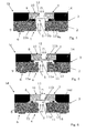
figure 2 is a section view of a first embodiment of an electronic device comprising MEMS devices according to the invention, -
figure 3 is a section view of a first version of the electronic device offigure 2 , -
figure 4 is a section view of a second version of the device offigure 2 , -
figure 5 is a section view of a third version of the device offigure 2 , -
figure 6 is a section view of a second embodiment of an electronic device comprising MEMS devices according to the invention, -
figure 7 is a section view of a third embodiment of an electronic device comprising MEMS devices according to the invention, -
figures 8 and 9 shows a section view of applications of the electronic devices comprising MEMS devices realised according to the invention, -
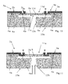
figures 10 and 11 are section view of known MEMS differential pressure sensors. - With reference to
figure 2 , a first embodiment is shown of anelectronic device 1 for MEMS differential sensor devices according to the invention which comprises asubstrate 2, for example of the LGA/BGA type, having anupper surface 3 and alower surface 4 opposed to theupper surface 3, provided with a passingopening 5 between these twosurfaces - In a known way a substrate of the LGA/BGA type is formed by conductive layers insulated from each other by means of layers of insulating or dielectric material. The conductive layers are conformed in conductive tracks insulated form each other by layers of insulating or dielectric material. Conductive holes, called "vias", are typically realised through the insulating layers with a vertical orientation with respect to the layers, to form conductive paths between conductive tracks belonging to different conductive layers.
- Moreover lands 6, connected to conductive tracks present on the
lower surface 4, are present on thelower surface 4 of thesubstrate 2. - The
electronic device 1 also comprises a MEMSdifferential sensor device 7 comprising adie 8, for example of silicon, having afirst surface 9 and asecond surface 10 opposed to thefirst surface 9. On the first surface 9 asensitive portion 11 of the MEMSdifferential sensor device 7 is integrated which leaves a firstactive surface 11a of thesensitive portion 11 exposed, while thesecond surface 10 is provided with anopening 12 which exposes a secondactive surface 11b, opposed to the firstactive surface 11a, of thesensitive portion 11. - According to the invention, the
first surface 9 of the MEMSdifferential sensor device 7 faces theupper surface 3 of thesubstrate 2 and is spaced therefrom by a determined distance and the sensitive portion 11 I aligned to theopening 5. - Moreover, the peripheral portion of the
first surface 9 of the MEMSdifferential sensor device 7 is provided with lands for the electric connection to conductive tracks present on theupper surface 3 of thesubstrate 2, by means ofelectric connections 13, for example bumps. - Advantageously, the MEMS
differential sensor device 7 is electrically mounted on thesubstrate 2 by means of the known "flip-chip" assembling method. - Still according to the invention, the
electronic device 1 comprises aprotective package 14, realised through moulding, which incorporates the MEMSdifferential sensor device 7, theelectric connections 13 and thesubstrate 2, leaving the firstactive surface 11a of thesensitive portion 11 of the MEMSdifferential sensor device 7 exposed through the passingopening 5 and the secondactive surface 11b of thesensitive portion 11 exposed through theopening 12 of thesecond surface 10. - Advantageously, the
protective package 14 leaves also thelower surface 4 of thesubstrate 2 exposed. - Advantageously, the
second surface 10 of the MEMSdifferential sensor device 7 flanked to an upper surface of theprotective package 14. - According to the invention, the
sensitive portion 11 is sensitive to chemical and/or physical variations of fluids present on or getting in contact with the twoactive surfaces sensitive portion 11. The fluids can be at least two, in such a case a first fluid interacts with the firstactive surface 11a of thesensitive portion 11 of the MEMSdifferential sensor device 7 through the passingopening 5, and the second fluid interacts with the secondactive surface 11b of thesensitive portion 11 of the MEMSdifferential sensor device 7 through theopening 12 provided on thesecond surface 10. - Advantageously, a
barrier element 15 is positioned between thefirst surface 9 of the MEMSdifferential sensor device 7 and theupper surface 3 of thesubstrate 2 so as to surround saidsensitive portion 11. - Advantageously according to the invention, the presence of this
barrier element 15 protects thesensitive portion 11 during the manufacturing process of theprotective package 14, though moulding, so that thissensitive portion 11 remains free. - In fact, in a known way, the formation of the
protective package 14 provides the introduction, inside a cavity of a mould, of thesubstrate 2 whereon the MEMSdifferential sensor device 7 is mounted. - In the mould cavity the injection is then provided, under pressure and at high temperature, of an electrically insulating material being melted, which will constitute the plastic body of the
protective package 14. This material is typically a synthetic resin, for example an epoxy resin. - The proper moulding step involves the injection of the resin into the cavity of the mould. This step is then followed by a cooling step for completing the
protective package 14. - For avoiding that the resin damages the
sensitive portion 11 of the MEMSdifferential sensor device 7 during the injection step of the resin, according to the invention, between theupper surface 3 of thesubstrate 2 and thefirst surface 9, thebarrier element 15 is provided which completely surrounds at least thesensitive portion 11 of the MEMSdifferential sensor device 7. - Advantageously, the
barrier element 15 is a ring which completely surrounds thesensitive portion 11 of theMEMS device 7, when theMEMS device 7 is mounted on thesubstrate 2, and contacts theupper surface 3 of thesubstrate 2 and thefirst surface 9 of the MEMSdifferential sensor device 7. - Advantageously, the
barrier element 15 is formed by a welding paste, thereby, in thus embodiment, the electric connection step and the gluing step of the MEMSdifferential sensor device 7 to thesubstrate 2 are carried out at the same time, resulting in a particularly compact structure of simple realisation, not needing critical alignments between different structures. - Moreover, the external edge of this
barrier element 15 is, for example, completely incorporated in theprotective package 14. - With reference to
figure 3 , a first embodiment is shown of an electronic device 1a according to the invention. - Elements being structurally and functionally identical with respect to the electric device described with reference to
figure 2 will be given the same reference numbers. - Advantageously, a
barrier element 15a is positioned at least in an area which surrounds thesensitive portion 11. - In this first embodiment, the
barrier element 15a i sanirregular area 15a formed on theupper surface 3 of thesubstrate 2. - Advantageously, this
irregular area 15a shows a corrugated surface. - Advantageously, this
irregular area 15a extends on theupper surface 3 of thesubstrate 2 in correspondence with the whole central free 3c. - Advantageously, according to the invention this
irregular area 15a is obtained by modifying the chemical properties of theupper surface 3 of thesubstrate 2, as shown infigure 3 . - Advantageously, the
irregular area 15a is formed by a non wettable material. - Nothing forbids that this
layer 15a of non wettable material is formed on theupper surface 3 of thesubstrate 2. - With reference to
figure 4 , a second version of the embodiment of an electronic device 1b according to the invention is shown. - Elements being structurally and functionally identical with respect to the
device 1 described with reference tofigure 2 will be given the same reference numbers. - Advantageously, a
barrier element 15b is positioned at least in an area which surrounds thesensitive portion 11. - In this second version, the
barrier element 15b is anirregular area 15b formed on thefirst surface 9 of the MEMSdifferential sensor device 7 and is obtained by modifying the chemical properties of thefirst surface 9 of the MEMSdifferential sensor device 7. - Advantageously, this
irregular area 15b extends on thefirst surface 9 of the MEMSdifferential sensor device 7 in correspondence with the wholesensitive portion 11 of the MEMSdifferential sensor device 7. - It is in fact known that a
silicon die 8, at least in correspondence with thefirst surface 9 of a MEMSdifferential sensor device 7, is coated by an insulating layer 9b of the non wettable type coated by a protection layer 9a comprising wettable material for example a plastic layer, for example comprising organic material such as Polyimide. - Advantageously, at least in correspondence with the
sensitive portion 11 of the MEMSdifferential sensor device 7, the layer of wettable material 9a is removed leaving the insulating layer 9b, for example formed by silicon oxide, exposed. - Advantageously, after the removal step from the
sensitive portion 11 of the MEMSdifferential sensor device 7 of the layer 9a of wettable material, the MEMS differential sensor device is welded onto thesubstrate 2 and is subjected to a cleaning operation for example in Plasma, by using a gas mixture including argon and oxygen. - Advantageously, the oxygen of the cleaning mixture chemically reacts with the layer 9a of wettable material increasing the wettability, while the dielectric layer 9b which coats the
sensitive portion 11 is inert to the treatment. - Therefore, as result after the treatment, an increased wettability is obtained of the layer 9a of wettable material, comparable to that of the
upper surface 3 of thesubstrate 2 and a reduced wettability of the surface of the dielectric layer 9b which coats thesensitive portion 11. - This wettability difference implies a sudden slow down of the resin flow during the moulding step of the
protective package 14 thereby the superficial voltage of the resin leads to the formation of a meniscus around the peripheral surface of the dielectric layer 9b which covers thesensitive portion 11. - Nothing forbids that a barrier layer 9b of non wettable material is formed not only on the
first surface 9 of the MEMS device, but also on theupper layer 3 of thesubstrate 2 aligned to thesensitive portion 11. - In a further version of these two latter embodiments of the invention the
irregular area - Advanatgeously, in the
irregular area differential sensor device 7, so as to realise a preferred path defined in thesubstrate 2 or on the MEMSdifferential sensor device 7 for the resin during the moulding step. - Advantageously, these trenches completely surround the
sensitive portion 11 of theMEMS device 7, as shown for example in thedevice 1c offigure 5 , wherein elements being structurally and functionally identical with respect to thedevice 1 described with reference tofigure 2 have been given the same reference numbers. - Advantageously, in this latter embodiment a layer of non wettable material can be present in correspondence with the
sensitive portion 11 of the MEMSdifferential sensor device 7 in correspondence with the area enclosed by the trenches, both on thesubstrate 2 and on the MEMSdifferential sensor device 7. - According to the invention, the presence of this
irregular area sensitive portion 11 during the manufacturing step of theprotective package 14, through moulding, so that the liquid resin is uniformly distributed around the electric connections without reaching thesensitive portion 11. - With reference to
figure 6 , a second embodiment of anelectronic device 1d according to the invention is shown. - Elements being structurally and functionally identical with respect to the
device 1 described with reference tofigure 2 will b given the same reference numbers. - In particular in this embodiment an
underfiller 16 incorporates theelectric connections 13 to mechanically strengthen theelectronic device 1 in the connection area between the MEMSdifferential sensor device 7 and thesubstrate 2. - Advantageously, the
underfiller 16 is formed by epoxy compounds, for example epoxy resin. - Advantageously, a
barrier element 15 can be provided between the MEMSdifferential sensor device 7 and thesubstrate 2. - Advantageously, the
underfiller 16 shows a tapered profile outwards of the MEMSdifferential sensor device 7, while it shows a substantially vertical profile in correspondence with thebarrier element 15. - In other words the cross section of the
underfiller 16 increases when approaching theupper surface 3 of thesubstrate 2. - The
electronic device 1d also comprises aprotective package 14d, realised through moulding, which incorporates the MEMSdifferential sensor device 7, theunderfiller 16 and thesubstrate 2, leaving the firstactive surface 11a of thesensitive portion 11 of the MEMSdifferential sensor device 7 exposed through the passingopening 5 of thesubstrate 2 and the secondactive surface 11b exposed through theopening 12 of thesecond surface 10. - Advantageously, the
protective package 14d leaves also thelower surface 4 of thesubstrate 2 exposed. - Advantageously, the
second surface 10 is flanked to an upper surface of theprotective package 14d. - The presence of the
barrier element 15 allows to maintain thesensitive portion 11 of the MEMSdifferential sensor device 7 free from theunderfiller 16. - Moreover, the
underfiller 16 protects thefirst surface 9 of the MEMSdifferential sensor device 7 during the manufacturing step of theplastic package 14d. - Advantageously, the
underfiller 16 is present outside thebarrier element figures 3 ,4 and 5 , at least in the area comprised between theupper surface 3 of thesubstrate 2 and thefirst surface 9 of the MEMSdifferential sensor device 7 so as to incorporate theelectric connections 13 for mechanically strengthen theelectronic device 1 in the connection area between the MEMSdifferential sensor device 7 and thesubstrate 2. - With reference to
figure 7 , a third embodiment of an electronic device 1e according to the invention is shown. - Elements being structurally and functionally identical with respect to the
device 1 described with reference tofigure 2 will be given the same reference numbers. - The electronic device 1e also comprises a
protective package 14e, realised through moulding, which incorporates the MEMSdifferential sensor device 7 and thesubstrate 2, leaving the firstactive surface 11a of thesensitive portion 11 of the MEMSdifferential sensor device 7 exposed through the passingopening 5, and advantageously, thelower surface 4 of thesubstrate 2. Theprotective package 14e coats thesecond surface 10 of the MEMSdifferential sensor device 7 and is provided with a further passingopening 17 aligned to theopening 12 present on thesecond surface 10 of the MEMSdifferential sensor device 7. - Advantageously, a
cylindrical projection 18 is formed on the passingopening 17 of theprotective package 14e to facilitate the access to thesensitive portion 11 of the MEMSdifferential sensor device 7. Advantageously, thiscylindrical projection 18 is realised simultaneously with theprotective package 14e during the same moulding step in which this package is formed. - Advantageously, a
barrier element 15 can be provided between the MEMSdifferential sensor device 7 and thesubstrate 2. - Advantageously, also in this embodiment of the invention the
barrier elements figures 3 to 5 or anunderfiller 16 like the one shown with reference tofigure 6 can be provided. - With reference to
figure 8 , thedevice 1 offigure 2 is shown wherein anintegrated circuit 19 is mounted on thesubstrate 2 flanked to the MEMSdifferential sensor device 7, and fixed onto thesubstrate 2 for example by means of a welding layer 20. - The
integrated circuit 19 is electrically connected to thesubstrate 2 by means of furtherelectric connections 21. - The
protective package 14, realised through moulding, incorporates the MEMSdifferential sensor device 7 with theelectric connections 13, theintegrated circuit 19 with the furtherelectric connections 21 and thesubstrate 2, leaving the firstactive surface 11a of thesensitive portion 11 of the MEMSdifferential sensor device 7 exposed through the passingopening 5 and the secondactive surface 11b of thesensitive portion 11 exposed through theopening 12 of thesecond surface 10. - Advantageously, the
protective package 14 leaves also thelower surface 4 of thesubstrate 2 exposed. - Advantageously, the
second surface 10 of the MEMSdifferential sensor device 7 is flanked to an upper surface of theprotective package 14. - With reference to
figure 9 , thedevice 1d offigure 6 is shown wherein anintegrated circuit 19 is mounted on thesubstrate 2 flanked to the MEMSdifferential sensor device 7, and fixed onto thesubstrate 2 for example by means of a welding layer 20. - The
integrated circuit 19 is electrically connected to thesubstrate 2 by means of furtherelectric connections 21. - The
protective package 14d, realised through moulding, incorporates the MEMSdifferential sensor device 7, theunderfiller 16, theintegrated circuit 19 with the furtherelectric connections 21 and thesubstrate 2, leaving the firstactive surface 11a of thesensitive portion 11 of the MEMSdifferential sensor device 7 exposed through the passingopening 5 and the secondactive surface 11b of thesensitive portion 11 exposed through theopening 12 of thesecond surface 10. - Advantageously, the
protective package 14d leaves also thelower surface 4 of thesubstrate 2 exposed. - Advantageously, the
second surface 10 of the MEMSdifferential device 7 is flanked to the upper surface of theprotective package 14d. - Advantageously, the MEMS
differential sensor device 7 used in the devices according to the invention is a differential pressure sensor device shown infigures 10 and 11 . - In particular, with reference to these figures, a
differential pressure sensor 7a is shown formed in asemiconductor die 8a for example of silicon. - In the semiconductor die 8a a
cavity 3a is realised next to afirst surface 9c of the semiconductor die 8a. - The portion of the semiconductor die 8a comprised between the
cavity 3a and thefirst surface 9c forms amembrane 11c, i.e. the sensitive element of thepressure sensor 7a. -
Resistive elements 6a are formed in the peripheral portion of themembrane 11c next to thefirst surface 9c. - An insulating
layer 4a, for example oxide, coats the firstactive surface 9c of thedie 2a, leaving a firstactive surface 11d of themembrane 11c, comprised between theresistive elements 6a, exposed. Moreover, openings are provided in the insulatinglayer 4a in correspondence with theseresistive elements 6a for allowing the electric connection to aconductive layer 2a which is formed on the insulatinglayer 4a. - Nothing forbids that the insulating layer coats the whole
active surface 9c of thedie 2a. - Advantageously, a passivation layer coats the first
active surface 9c of thedie 2a. - In particular, the
conductive layer 2a comprises twoportions resistive elements 6a. - An
opening second surface 10a of thesensor 7a, opposed to thefirst surface 9c, which puts thecavity 3a in communication with the outside of thesensor 7a. In this way theopening active surface 11e of themembrane 11c which is faced in thecavity 3a. - As shown in
figure 10 , if theopening 12a is realised through a dry etching, the walls of theopening 12a are substantially perpendicular with respect to thesecond surface 10a, i.e. the cross dimensions of theopening 12a are substantially constant. - As shown in
figure 11 instead, if theopening 12b is realised through an etching of the wet type the walls of theopening 12b are tapered, i.e. the cross dimensions of theopening 12b decrease when departing from thesecond surface 10a. - In conclusion, with the device according to the invention it is possible to realise microphones, pressure, gas, chemical differential sensors, which are encapsulated in a protective package realised trough moulding.
- According to the invention it is also possible to integrate more sensors (accelerometers and pressure sensors) in the same
protective package 14. - Advantageously, in a preferred embodiment, the overall
electronic device differential sensor device 7 shows a width of 1500 µm a length of 1500 µm and a thickness 700 µm and shows anopening 12 on thesecond surface 10 comprised between 100 and 500 µm. - The
sensitive portion 11 of the MEMSdifferential sensor device 7 is of circular or squared shape and has a diameter / side comprised between 100 µm and 1000 µm. - The distance between the
first surface 9 of the MEMSdifferential sensor device 7 and theupper surface 3 of the substrate is comprised between 50 and 500 µm, while the thickness of thesubstrate 2 is comprised between 150 and 300 µm, while the width of theopening 5 is comprised between 100 and 700um. - If the
barrier element 15 is realised by a ring of welding paste it has a thickness of a cross section comprised between 60 and 300 µm. - If the
barrier element - In conclusion, the electronic device according to the invention is particularly compact and uses technical solutions which do not provide critical alignments.
- Advantageously, the presence of the
barrier element sensitive portion 11 of the MEMSdifferential sensor device 7 during the manufacturing steps of theprotective package 14 or during the dispensing step of theunderfiller 16 in theelectronic device 1 according to the invention. - Advantageously, this
barrier element substrate 2 and on the MEMSdifferential sensor device 7.
Claims (32)
- Electronic device (1, 1a, 1b, 1c, 1d, 1e) comprising:- a substrate (2) provided with at least one passing opening (5),- a MEMS device (7) with function of differential sensor provided with a first and a second surface (9, 10) and of the type comprising at least one portion (11) sensitive to chemical and/or physical variations of fluids present in correspondence with a first and second opposed active surface (11a, 11b) thereof, said first surface (9) of said MEMS device (7) leaving said first active surface (11a) exposed and said second surface (10) being provided with a further opening (12) which exposes said second active opposed surface (11b), the electronic device (1, 1d, 1e) being characterised in that said first surface (9) of said MEMS device (7) faces said substrate (2) and is spaced therefrom by a determined distance, said sensitive portion (11) being aligned to said passing opening (5) of said substrate (2), and- a protective package (14, 14a, 14b), which incorporates at least partially said MEMS device (7) and said substrate (2) so as to leave said first and second opposed active surfaces (11a, 11b) exposed respectively through said passing opening (5) of said substrate (2) and said further opening (12) of said second surface (10),
characterized in that it further comprises:a barrier element (15, 15a, 15b) which surrounds said sensitive portion (11) for realising a protection structure for said MEMS differential sensor device (7), so that said first active surface (11a) of said sensitive portion (11) is free. - Electronic device (1) according to claim 1, characterised in that said barrier element (15) is of welding paste.
- Electronic device (1) according to claim 1, characterised in that said barrier element (15a) is an irregular area (15a) formed on the upper surface (3) of the substrate (2).
- Electronic device (1) according to claim 1, characterised in that this irregular area (15a), extends on the upper surface (3) of said substrate (2) in correspondence with said sensitive portion (11).
- Electronic device (1) according to claim 3 or 4, characterised in that this irregular area (15a) is obtained by modifying the chemical properties of the upper surface (3) of the substrate (2).
- Electronic device (1) according to claim 3 or 4, characterised in that said irregular area (15a) is formed by non wettable material.
- Electronic device (1) according to claim 1, characterised in that said barrier element (15b) is an irregular area (15b) formed on said first surface (9) of the MEMS differential sensor device (7).
- Electronic device (1) according to claim 7, characterised in that this irregular area (15b), extends on the sensitive portion (11) of the MEMS differential sensor device (7).
- Electronic device (1) according to claim 7 or 8, characterised in that this irregular area (15b) is obtained by modifying the chemical properties around said first surface (9) of the MEMS differential sensor device (7).
- Electronic device (1) according to claim 7 or 8, characterised in that said irregular area (15b) is formed by non wettable material.
- Electronic device (1) according to claim 10, wherein said first active surface (11a) of said sensitive portion (11) is coated by a non wettable insulating layer (9b) and a protection layer (9a) characterised in that said irregular area (15b) is formed through removal of said protection layer (9a) from said first surface (9) of the MEMS differential sensor device (7) for exposing said layer (9b) of non wettable material.
- Electronic device (1) according to claim 11, characterised in that said protection layer (9a) is Polyimide and said layer (9b) of non wettable material is oxide.
- Electronic device (1) according to claim 3 or 7, characterised in that said irregular area (15a, 15b) comprises trenches which form preferred paths during the formation steps of the protective package.
- Electronic device (1) according to claim 13, characterised in that a layer of non wettable material is formed in correspondence with said sensitive portion (11) of said MEMS differential sensor device (7).
- Electronic device (1) according to claim 1, characterised in that said second surface (10) is flanked to an upper surface of said protective package (14).
- Electronic device (1) according to claim 1, characterised in that said protective package (14e) also coats said second surface (10) and is provided with a passing opening (17) aligned to the opening (12) present on said second surface (10) of said MEMS differential sensor device (7).
- Electronic device (1) according to claim 16, characterised in that a cylindrical projection (18) is formed on said passing opening (17) of said protective package (14e) to facilitate the access to said sensitive portion (11) of said MEMS differential sensor device (7).
- Electronic device (1) according to claim 1, characterised in that electric connection (13) which electrically couple said MEMS differential sensor device (7) to said substrate (2) are present outside said barrier element (15, 15a) with respect to said sensitive portion (11).
- Electronic device (1) according to claim 18, characterised in that an underfiller (16) incorporates said electric connections (13).
- Electronic device (1) according to claim 19, characterised in that a barrier element (15, 15a, 15b) protects the sensitive portion (11) during the formation of said underfiller (16)
- Electronic device (1) according to claim 19, characterised in that said underfiller (16) shows a tapered profile outside said peripheral area, while it shows a substantially vertical profile in correspondence with said area which surrounds said sensitive portion (11).
- Electronic device (1) according to claim 7, characterised in that said electric connections (13) comprise bumps.
- Electronic device (1) according to claim 1, characterised in that said MEMS differential sensor device (7) is mounted on said substrate (2) through the known "flip-chip" assembling method.
- Electronic device (1) according to claim 1, characterised in that it comprises integrated circuits (19) mounted flanked to the MEMS differential sensor device (7).
- Electronic device (1) according to claim 1, characterised in that said integrated circuits (19) are electrically connected to conductive tracks present on said substrate (2), by means of further electric connections (21).
- Electronic device (1) according to claim 23, characterised in that said protective package (14) incorporates said integrated circuits (19) and said further electric connections (21).
- Electronic device (1) according to claim 1, characterised in that said substrate is of the LGA type.
- Electronic device (1) according to claim 1, characterised in that said substrate is of the BGA type.
- Electronic device (1) according to claim 1, characterised in that said MEMS differential sensor device (7) is a pressure sensor.
- Electronic device (1) according to claim 1, characterised in that said MEMS device is a gas sensor.
- Electronic device (1) according to claim 1, characterised in that said MEMS device is a chemical sensor.
- Electronic device (1) according to claim 1, characterised in that said protective package (14) is realised through moulding.
Applications Claiming Priority (2)
| Application Number | Priority Date | Filing Date | Title |
|---|---|---|---|
| IT000099A ITMI20070099A1 (en) | 2007-01-24 | 2007-01-24 | ELECTRONIC DEVICE INCLUDING DIFFERENTIAL SENSOR DEVICES MEMS AND SUBSTRATES LAUNDRY |
| EP08707208.8A EP2121513B1 (en) | 2007-01-24 | 2008-01-23 | Electronic device comprising differential sensor mems devices and drilled substrates |
Related Parent Applications (2)
| Application Number | Title | Priority Date | Filing Date |
|---|---|---|---|
| EP08707208.8 Division | 2008-01-23 | ||
| EP08707208.8A Division-Into EP2121513B1 (en) | 2007-01-24 | 2008-01-23 | Electronic device comprising differential sensor mems devices and drilled substrates |
Publications (2)
| Publication Number | Publication Date |
|---|---|
| EP2644563A2 true EP2644563A2 (en) | 2013-10-02 |
| EP2644563A3 EP2644563A3 (en) | 2013-12-04 |
Family
ID=39473216
Family Applications (2)
| Application Number | Title | Priority Date | Filing Date |
|---|---|---|---|
| EP13169983.7A Withdrawn EP2644563A3 (en) | 2007-01-24 | 2008-01-23 | Electronic device comprising differential MEMS sensor and substrate having through hole |
| EP08707208.8A Active EP2121513B1 (en) | 2007-01-24 | 2008-01-23 | Electronic device comprising differential sensor mems devices and drilled substrates |
Family Applications After (1)
| Application Number | Title | Priority Date | Filing Date |
|---|---|---|---|
| EP08707208.8A Active EP2121513B1 (en) | 2007-01-24 | 2008-01-23 | Electronic device comprising differential sensor mems devices and drilled substrates |
Country Status (6)
| Country | Link |
|---|---|
| US (3) | US8134214B2 (en) |
| EP (2) | EP2644563A3 (en) |
| JP (1) | JP5619425B2 (en) |
| CN (1) | CN101616863B (en) |
| IT (1) | ITMI20070099A1 (en) |
| WO (1) | WO2008089969A2 (en) |
Cited By (1)
| Publication number | Priority date | Publication date | Assignee | Title |
|---|---|---|---|---|
| DE102020212123A1 (en) | 2020-09-25 | 2021-12-16 | Robert Bosch Gesellschaft mit beschränkter Haftung | Sensor and method of manufacturing a sensor |
Families Citing this family (49)
| Publication number | Priority date | Publication date | Assignee | Title |
|---|---|---|---|---|
| ITMI20070099A1 (en) | 2007-01-24 | 2008-07-25 | St Microelectronics Srl | ELECTRONIC DEVICE INCLUDING DIFFERENTIAL SENSOR DEVICES MEMS AND SUBSTRATES LAUNDRY |
| US7992441B2 (en) * | 2008-07-31 | 2011-08-09 | Sensata Technologies, Inc. | Pressure sensor for measuring pressure in a medium |
| US7900521B2 (en) | 2009-02-10 | 2011-03-08 | Freescale Semiconductor, Inc. | Exposed pad backside pressure sensor package |
| US8359927B2 (en) | 2009-08-12 | 2013-01-29 | Freescale Semiconductor, Inc. | Molded differential PRT pressure sensor |
| EP2320453A1 (en) * | 2009-11-06 | 2011-05-11 | Nxp B.V. | Sensor packaging |
| DE102010001711A1 (en) * | 2010-02-09 | 2011-08-11 | Robert Bosch GmbH, 70469 | Semiconductor device and corresponding manufacturing method |
| DE102010022204B4 (en) * | 2010-05-20 | 2016-03-31 | Epcos Ag | Electric component with flat design and manufacturing process |
| JP2012073233A (en) * | 2010-08-31 | 2012-04-12 | Mitsumi Electric Co Ltd | Sensor device and mounting method of semiconductor sensor element |
| US8569861B2 (en) | 2010-12-22 | 2013-10-29 | Analog Devices, Inc. | Vertically integrated systems |
| DE102011006517A1 (en) | 2011-03-31 | 2012-10-04 | Endress + Hauser Gmbh + Co. Kg | Flameproof encapsulated differential pressure sensor |
| DE102011007604A1 (en) * | 2011-04-18 | 2012-10-18 | Robert Bosch Gmbh | Microelectromechanical sound detection device and method for producing such |
| KR101881732B1 (en) * | 2011-06-30 | 2018-07-27 | 무라타 일렉트로닉스 오와이 | A method of making a system-in-package device, and a system-in-package device |
| DE102012203373A1 (en) * | 2012-03-05 | 2013-09-05 | Robert Bosch Gmbh | Micromechanical sound transducer arrangement and a corresponding manufacturing method |
| US9402138B2 (en) | 2012-10-12 | 2016-07-26 | Infineon Technologies Ag | MEMS device and method of manufacturing a MEMS device |
| US8946833B2 (en) * | 2012-10-22 | 2015-02-03 | Freescale Semiconductor, Inc. | Packaging for semiconductor sensor devices and methods |
| JP2014126507A (en) * | 2012-12-27 | 2014-07-07 | Bosch Corp | Pressure sensor module |
| EP2759832B1 (en) * | 2013-01-23 | 2020-11-11 | Sciosense B.V. | Electrochemical sensor device |
| US20140374848A1 (en) * | 2013-06-24 | 2014-12-25 | Wen Shi Koh | Semiconductor sensor device with metal lid |
| US9627229B2 (en) * | 2013-06-27 | 2017-04-18 | STATS ChipPAC Pte. Ltd. | Semiconductor device and method of forming trench and disposing semiconductor die over substrate to control outward flow of underfill material |
| JP6339669B2 (en) | 2013-07-08 | 2018-06-06 | モーション・エンジン・インコーポレーテッド | MEMS device and method of manufacturing |
| US10273147B2 (en) | 2013-07-08 | 2019-04-30 | Motion Engine Inc. | MEMS components and method of wafer-level manufacturing thereof |
| ITTO20130651A1 (en) | 2013-07-31 | 2015-02-01 | St Microelectronics Srl | PROCESS OF MANUFACTURING AN ENCAPSULATED DEVICE, IN PARTICULAR AN ENCAPSULATED MICRO-ELECTRO-MECHANICAL SENSOR, EQUIPPED WITH AN ACCESSIBLE STRUCTURE, AS A MEMS MICROPHONE AND ENCAPSULATED DEVICE SO OBTAINED |
| WO2015013828A1 (en) | 2013-08-02 | 2015-02-05 | Motion Engine Inc. | Mems motion sensor and method of manufacturing |
| EP2857349B1 (en) * | 2013-10-01 | 2020-08-05 | LG Innotek Co., Ltd. | Gas sensor package |
| CN103539063A (en) * | 2013-11-05 | 2014-01-29 | 华进半导体封装先导技术研发中心有限公司 | Environment micro electrical mechanical system (MEMS) sensor base plate packaging structure and manufacturing method |
| US9190352B2 (en) | 2013-11-21 | 2015-11-17 | Freescale Semiconductor, Inc. | Multi-die sensor device |
| EP2884242B1 (en) | 2013-12-12 | 2021-12-08 | ams International AG | Sensor Package And Manufacturing Method |
| SG10201408698SA (en) * | 2013-12-26 | 2015-07-30 | Agency Science Tech & Res | Chemical Sensor Package For Highly Pressured Environment |
| WO2015103688A1 (en) | 2014-01-09 | 2015-07-16 | Motion Engine Inc. | Integrated mems system |
| TWI538113B (en) * | 2014-02-14 | 2016-06-11 | 南茂科技股份有限公司 | Microelectromechanical chip package and method of manufacturing same |
| US20170030788A1 (en) | 2014-04-10 | 2017-02-02 | Motion Engine Inc. | Mems pressure sensor |
| WO2015184531A1 (en) | 2014-06-02 | 2015-12-10 | Motion Engine Inc. | Multi-mass mems motion sensor |
| US10190931B2 (en) * | 2014-09-03 | 2019-01-29 | Cometnetwork Co., Ltd. | Differential pressure sensor |
| US9638597B2 (en) * | 2014-09-24 | 2017-05-02 | Nxp Usa, Inc. | Differential pressure sensor assembly |
| WO2016090467A1 (en) | 2014-12-09 | 2016-06-16 | Motion Engine Inc. | 3d mems magnetometer and associated methods |
| CN107110726A (en) * | 2014-12-24 | 2017-08-29 | 株式会社藤仓 | Pressure sensor and pressure sensor module |
| CA3220839A1 (en) | 2015-01-15 | 2016-07-21 | Motion Engine Inc. | 3d mems device with hermetic cavity |
| DE102015104257A1 (en) * | 2015-03-20 | 2016-09-22 | Rheinische Friedrich-Wilhelms-Universität Bonn | Sensor for determining pressure and / or flow |
| US9778129B2 (en) * | 2015-08-03 | 2017-10-03 | DunAn Sensing, LLC | Universal hermetically sealed button pressure sensor |
| DE102015116081A1 (en) | 2015-09-23 | 2017-03-23 | Infineon Technologies Ag | An electronic sensor device comprising a flip-chip mounted semiconductor chip and a substrate having an opening |
| FR3047560B1 (en) * | 2016-02-10 | 2018-03-16 | Jtekt Europe | METHOD FOR MANUFACTURING A TORQUE SENSOR COMPRISING AN ENCAPSULATION STEP OF THE SENSOR ELECTRONIC CIRCUIT |
| US10466125B2 (en) * | 2016-11-11 | 2019-11-05 | Measurement Specialties Inc. | Pressure sensor sub assembly and fabrication |
| IT201600121210A1 (en) | 2016-11-30 | 2018-05-30 | St Microelectronics Srl | MULTI-DEVICE TRANSDUCTION MODULE, ELECTRONIC EQUIPMENT INCLUDING THE TRANSDUCTION FORM AND METHOD OF MANUFACTURING THE TRANSDUCTION MODULE |
| EP3625554A1 (en) | 2017-05-15 | 2020-03-25 | Analog Devices Global Unlimited Company | Integrated ion sensing apparatus and methods |
| US10373883B2 (en) * | 2017-10-26 | 2019-08-06 | Advanced Semiconductor Engineering, Inc. | Semiconductor package device and method of manufacturing the same |
| US10730743B2 (en) | 2017-11-06 | 2020-08-04 | Analog Devices Global Unlimited Company | Gas sensor packages |
| CN108996467A (en) * | 2018-08-08 | 2018-12-14 | 宁波琻捷电子科技有限公司 | Sensor-packaging structure and method |
| US11587839B2 (en) | 2019-06-27 | 2023-02-21 | Analog Devices, Inc. | Device with chemical reaction chamber |
| US12474290B2 (en) | 2019-11-20 | 2025-11-18 | Analog Devices International Unlimited Company | Electrochemical device |
Family Cites Families (32)
| Publication number | Priority date | Publication date | Assignee | Title |
|---|---|---|---|---|
| JPS5828754B2 (en) * | 1977-05-19 | 1983-06-17 | 株式会社デンソー | Pressure-electric conversion device |
| US4763098A (en) * | 1985-04-08 | 1988-08-09 | Honeywell Inc. | Flip-chip pressure transducer |
| US5658828A (en) | 1989-11-30 | 1997-08-19 | Sgs-Thomson Microelectronics, Inc. | Method for forming an aluminum contact through an insulating layer |
| US5189777A (en) | 1990-12-07 | 1993-03-02 | Wisconsin Alumni Research Foundation | Method of producing micromachined differential pressure transducers |
| DE4207225C2 (en) | 1992-03-07 | 1994-06-16 | Bosch Gmbh Robert | Integrated circuit with adjustment components |
| US6140144A (en) * | 1996-08-08 | 2000-10-31 | Integrated Sensing Systems, Inc. | Method for packaging microsensors |
| JPH10274583A (en) * | 1997-03-31 | 1998-10-13 | Matsushita Electric Works Ltd | Semiconductor pressure sensor |
| US5923995A (en) | 1997-04-18 | 1999-07-13 | National Semiconductor Corporation | Methods and apparatuses for singulation of microelectromechanical systems |
| JPH11230846A (en) * | 1998-02-09 | 1999-08-27 | Denso Corp | Method of manufacturing semiconductor dynamic quantity sensor |
| JP3567740B2 (en) * | 1998-07-02 | 2004-09-22 | オムロン株式会社 | Semiconductor sensor and mounting structure |
| US6346742B1 (en) * | 1998-11-12 | 2002-02-12 | Maxim Integrated Products, Inc. | Chip-scale packaged pressure sensor |
| FR2801971B1 (en) | 1999-12-07 | 2002-02-15 | St Microelectronics Sa | INTEGRATED ACOUSTIC TRANSMITTER AND RECEIVER, AND MANUFACTURING METHOD THEREOF |
| US7434305B2 (en) | 2000-11-28 | 2008-10-14 | Knowles Electronics, Llc. | Method of manufacturing a microphone |
| US7439616B2 (en) | 2000-11-28 | 2008-10-21 | Knowles Electronics, Llc | Miniature silicon condenser microphone |
| US7166910B2 (en) | 2000-11-28 | 2007-01-23 | Knowles Electronics Llc | Miniature silicon condenser microphone |
| DE10059813A1 (en) * | 2000-12-01 | 2002-06-13 | Hahn Schickard Ges | Pressure measurement, especially differential pressure measurement between two fluids, in which gluing of support and pressure sensor is used |
| US6432737B1 (en) * | 2001-01-03 | 2002-08-13 | Amkor Technology, Inc. | Method for forming a flip chip pressure sensor die package |
| DE10205127A1 (en) * | 2002-02-07 | 2003-08-28 | Infineon Technologies Ag | Semiconductor component with sensor or actuator surface and method for its production |
| US6850133B2 (en) | 2002-08-14 | 2005-02-01 | Intel Corporation | Electrode configuration in a MEMS switch |
| DE10238581B4 (en) * | 2002-08-22 | 2008-11-27 | Qimonda Ag | Semiconductor component |
| US6781231B2 (en) | 2002-09-10 | 2004-08-24 | Knowles Electronics Llc | Microelectromechanical system package with environmental and interference shield |
| JP2004177343A (en) | 2002-11-28 | 2004-06-24 | Fujikura Ltd | Pressure sensor |
| US7382048B2 (en) | 2003-02-28 | 2008-06-03 | Knowles Electronics, Llc | Acoustic transducer module |
| US7501703B2 (en) | 2003-02-28 | 2009-03-10 | Knowles Electronics, Llc | Acoustic transducer module |
| US7262509B2 (en) * | 2004-05-11 | 2007-08-28 | Intel Corporation | Microelectronic assembly having a perimeter around a MEMS device |
| WO2006061025A2 (en) * | 2004-12-09 | 2006-06-15 | Inverness Medical Switzerland Gmbh | A method of producing a micro fluidic device and a micro fluidic device |
| EP1719993A1 (en) * | 2005-05-06 | 2006-11-08 | STMicroelectronics S.r.l. | Integrated differential pressure sensor and manufacturing process thereof |
| EP1775259A1 (en) | 2005-10-14 | 2007-04-18 | STMicroelectronics S.r.l. | Wafer level package for sensor devices |
| US20070215962A1 (en) | 2006-03-20 | 2007-09-20 | Knowles Elecronics, Llc | Microelectromechanical system assembly and method for manufacturing thereof |
| JP5248317B2 (en) * | 2006-11-29 | 2013-07-31 | 株式会社フジクラ | Pressure sensor module |
| ITMI20070099A1 (en) | 2007-01-24 | 2008-07-25 | St Microelectronics Srl | ELECTRONIC DEVICE INCLUDING DIFFERENTIAL SENSOR DEVICES MEMS AND SUBSTRATES LAUNDRY |
| TWI364804B (en) * | 2007-11-14 | 2012-05-21 | Ind Tech Res Inst | Wafer level sensor package structure and method therefor |
-
2007
- 2007-01-24 IT IT000099A patent/ITMI20070099A1/en unknown
-
2008
- 2008-01-23 JP JP2009546683A patent/JP5619425B2/en active Active
- 2008-01-23 WO PCT/EP2008/000495 patent/WO2008089969A2/en not_active Ceased
- 2008-01-23 EP EP13169983.7A patent/EP2644563A3/en not_active Withdrawn
- 2008-01-23 CN CN2008800030368A patent/CN101616863B/en active Active
- 2008-01-23 EP EP08707208.8A patent/EP2121513B1/en active Active
-
2009
- 2009-07-24 US US12/508,869 patent/US8134214B2/en active Active
-
2012
- 2012-01-25 US US13/358,318 patent/US8796059B2/en active Active
-
2013
- 2013-05-31 US US13/907,077 patent/US8847340B2/en active Active
Non-Patent Citations (1)
| Title |
|---|
| None |
Cited By (1)
| Publication number | Priority date | Publication date | Assignee | Title |
|---|---|---|---|---|
| DE102020212123A1 (en) | 2020-09-25 | 2021-12-16 | Robert Bosch Gesellschaft mit beschränkter Haftung | Sensor and method of manufacturing a sensor |
Also Published As
| Publication number | Publication date |
|---|---|
| CN101616863B (en) | 2013-08-21 |
| CN101616863A (en) | 2009-12-30 |
| US8796059B2 (en) | 2014-08-05 |
| US8847340B2 (en) | 2014-09-30 |
| US20120164775A1 (en) | 2012-06-28 |
| US20090278215A1 (en) | 2009-11-12 |
| EP2121513B1 (en) | 2015-01-21 |
| JP5619425B2 (en) | 2014-11-05 |
| US8134214B2 (en) | 2012-03-13 |
| EP2644563A3 (en) | 2013-12-04 |
| WO2008089969A2 (en) | 2008-07-31 |
| EP2121513A2 (en) | 2009-11-25 |
| JP2010517021A (en) | 2010-05-20 |
| ITMI20070099A1 (en) | 2008-07-25 |
| US20130264662A1 (en) | 2013-10-10 |
| WO2008089969A3 (en) | 2008-12-31 |
Similar Documents
| Publication | Publication Date | Title |
|---|---|---|
| EP2121513B1 (en) | Electronic device comprising differential sensor mems devices and drilled substrates | |
| US8043881B2 (en) | Electronic device including MEMS devices and holed substrates, in particular of the LGA or BGA type | |
| US9771259B2 (en) | Method for fabricating electronic device package | |
| CN104303262B (en) | Process for Hermetic MEMS Devices Parts of which Are Exposed to the Environment | |
| TWI455265B (en) | Package structure with MEMS components and its manufacturing method | |
| CN115403005B (en) | Pressure sensing module, resistance type pressure sensor and manufacturing method thereof | |
| KR102313151B1 (en) | Method for Fabricating Stress Decoupled Micromechanical Pressure Sensors | |
| KR100620810B1 (en) | MEMS device package and manufacturing method thereof | |
| US20090315169A1 (en) | Frame and method of manufacturing assembly | |
| CN112110409B (en) | Semiconductor device and method for manufacturing semiconductor device | |
| US11760623B2 (en) | No-gel pressure sensor package | |
| CN102464294B (en) | Manufacturing method of package structure with microelectromechanical components | |
| US7696083B2 (en) | Multi-layer device | |
| US6593651B1 (en) | Terminals for multi-layer devices | |
| ITMI20070008A1 (en) | ELECTRONIC DEVICE INCLUDING MEMS AND SUBSTRATES HANGED IN PARTICULAR OF LGA OR BGA TYPE | |
| KR20160135528A (en) | Sensor package and manufacturing method thereof |
Legal Events
| Date | Code | Title | Description |
|---|---|---|---|
| PUAI | Public reference made under article 153(3) epc to a published international application that has entered the european phase |
Free format text: ORIGINAL CODE: 0009012 |
|
| AC | Divisional application: reference to earlier application |
Ref document number: 2121513 Country of ref document: EP Kind code of ref document: P |
|
| AK | Designated contracting states |
Kind code of ref document: A2 Designated state(s): AT BE BG CH CY CZ DE DK EE ES FI FR GB GR HR HU IE IS IT LI LT LU LV MC MT NL NO PL PT RO SE SI SK TR |
|
| PUAL | Search report despatched |
Free format text: ORIGINAL CODE: 0009013 |
|
| AK | Designated contracting states |
Kind code of ref document: A3 Designated state(s): AT BE BG CH CY CZ DE DK EE ES FI FR GB GR HR HU IE IS IT LI LT LU LV MC MT NL NO PL PT RO SE SI SK TR |
|
| RIC1 | Information provided on ipc code assigned before grant |
Ipc: B81B 7/00 20060101AFI20131031BHEP Ipc: G01L 19/00 20060101ALI20131031BHEP Ipc: G01D 11/24 20060101ALI20131031BHEP Ipc: G01L 13/02 20060101ALI20131031BHEP |
|
| STAA | Information on the status of an ep patent application or granted ep patent |
Free format text: STATUS: THE APPLICATION IS DEEMED TO BE WITHDRAWN |
|
| 18D | Application deemed to be withdrawn |
Effective date: 20140605 |