EP2642668A1 - Transmitter and Receiver for Reducing Power Consumption in FM-UWB Communication System - Google Patents
Transmitter and Receiver for Reducing Power Consumption in FM-UWB Communication System Download PDFInfo
- Publication number
- EP2642668A1 EP2642668A1 EP13159692.6A EP13159692A EP2642668A1 EP 2642668 A1 EP2642668 A1 EP 2642668A1 EP 13159692 A EP13159692 A EP 13159692A EP 2642668 A1 EP2642668 A1 EP 2642668A1
- Authority
- EP
- European Patent Office
- Prior art keywords
- signal
- frequency
- uwb
- generated
- modulator
- Prior art date
- Legal status (The legal status is an assumption and is not a legal conclusion. Google has not performed a legal analysis and makes no representation as to the accuracy of the status listed.)
- Granted
Links
Images




Classifications
-
- H—ELECTRICITY
- H04—ELECTRIC COMMUNICATION TECHNIQUE
- H04W—WIRELESS COMMUNICATION NETWORKS
- H04W52/00—Power management, e.g. Transmission Power Control [TPC] or power classes
- H04W52/02—Power saving arrangements
- H04W52/0209—Power saving arrangements in terminal devices
- H04W52/0261—Power saving arrangements in terminal devices managing power supply demand, e.g. depending on battery level
- H04W52/0274—Power saving arrangements in terminal devices managing power supply demand, e.g. depending on battery level by switching on or off the equipment or parts thereof
- H04W52/028—Power saving arrangements in terminal devices managing power supply demand, e.g. depending on battery level by switching on or off the equipment or parts thereof switching on or off only a part of the equipment circuit blocks
-
- H—ELECTRICITY
- H04—ELECTRIC COMMUNICATION TECHNIQUE
- H04B—TRANSMISSION
- H04B14/00—Transmission systems not characterised by the medium used for transmission
- H04B14/02—Transmission systems not characterised by the medium used for transmission characterised by the use of pulse modulation
-
- H—ELECTRICITY
- H04—ELECTRIC COMMUNICATION TECHNIQUE
- H04B—TRANSMISSION
- H04B1/00—Details of transmission systems, not covered by a single one of groups H04B3/00 - H04B13/00; Details of transmission systems not characterised by the medium used for transmission
- H04B1/69—Spread spectrum techniques
- H04B1/7163—Spread spectrum techniques using impulse radio
- H04B1/71632—Signal aspects
-
- H—ELECTRICITY
- H04—ELECTRIC COMMUNICATION TECHNIQUE
- H04L—TRANSMISSION OF DIGITAL INFORMATION, e.g. TELEGRAPHIC COMMUNICATION
- H04L27/00—Modulated-carrier systems
- H04L27/10—Frequency-modulated carrier systems, i.e. using frequency-shift keying
-
- Y—GENERAL TAGGING OF NEW TECHNOLOGICAL DEVELOPMENTS; GENERAL TAGGING OF CROSS-SECTIONAL TECHNOLOGIES SPANNING OVER SEVERAL SECTIONS OF THE IPC; TECHNICAL SUBJECTS COVERED BY FORMER USPC CROSS-REFERENCE ART COLLECTIONS [XRACs] AND DIGESTS
- Y02—TECHNOLOGIES OR APPLICATIONS FOR MITIGATION OR ADAPTATION AGAINST CLIMATE CHANGE
- Y02D—CLIMATE CHANGE MITIGATION TECHNOLOGIES IN INFORMATION AND COMMUNICATION TECHNOLOGIES [ICT], I.E. INFORMATION AND COMMUNICATION TECHNOLOGIES AIMING AT THE REDUCTION OF THEIR OWN ENERGY USE
- Y02D30/00—Reducing energy consumption in communication networks
- Y02D30/70—Reducing energy consumption in communication networks in wireless communication networks
Definitions
- FM-UWB frequency modulation-ultra-wideband
- Ultra-wideband has drawn attention as a very promising technology in the fields of wireless communications, imaging, and sensors, as its capabilities of transmitting multimedia data at a high speed of hundreds of megabits per second (Mbps) to 1 gigabit per second (Gbps) and of detecting a precise location are highlighted.
- Mbps megabits per second
- Gbps gigabit per second
- UWB has been permitted for commercial use in the field of wireless communications, various attempts have been made to use UWB in short-range wireless personal area networks.
- UWB The Federal Communications Commission in the United States has defined UWB as a wireless communication technology including a spectrum that occupies a bandwidth greater than or equal to 20% of a center frequency, or a bandwidth of at least 500 megahertz (MHz). Accordingly, existing carrier modulation including a spectrum that occupies a bandwidth of at least 500 MHz may be considered as UWB.
- UWB is regarded as a low-power, high-speed, short-range wireless communication technology that may perform communication in a range from 3.1 to 10.6 gigahertz (GHz) at a rate of 100 Mbps or more over a band wider than that of a conventional communication technology.
- GHz gigahertz
- a UWB system is based on a lower power spectral density over a very wide frequency band than that of a conventional narrowband system or a wideband code division multiple access (CDMA) system. Since the UWB system spreads and transmits a signal over a bandwidth of several GHz in order to prevent interference with another communication system, the UWB system may provide communications without interfering with another narrowband signal and without being greatly affected by a frequency. As a result, the UWB system may share a frequency spectrum and require very low power.
- CDMA wideband code division multiple access
- UWB has been studied in Institute of Electrical and Electronics Engineers (IEEE) 802.15.3a, which is a UWB standard for a wireless personal area network (WPAN), and in IEEE 802.15.4A, which is a UWB standard for a low-rate and low-power WPAN including a wireless positioning function.
- IEEE 802.15.3a which is a UWB standard for a wireless personal area network (WPAN)
- IEEE 802.15.4A which is a UWB standard for a low-rate and low-power WPAN including a wireless positioning function.
- an impulse radio (IR)-UWB system includes a transmitter that discontinuously transmits a Gaussian monocycle pulse or a pulse with a narrow width of 1 nanosecond (ns) or so. Accordingly, the IR-UWB system may transmit a signal using a much wider band (hundreds of MHz to several GHz) than a data modulation band, and thus, may greatly reduce a power spectral density, thereby reducing interference. Also, since the IR-UWB system uses such a pulse, the IR-UWB system is very resilient to multi-path fading.
- the IR-UWB system modulates a baseband signal into an impulse signal, and directly transmits the impulse signal. Accordingly, the IR-UWB system may be simply constructed at low cost.
- a transmitter including a detector configured to generate a pulse signal when an edge of a digital signal is detected.
- the transmitter further includes a first modulator configured to modulate the digital signal into a first modulation signal based on a value of the digital signal.
- the transmitter further includes a second modulator configured to modulate the first modulation signal into a second modulation signal based on a frequency of the first modulation signal when the pulse signal is generated.
- the second modulator may be further configured to be cut off from a power supply when the pulse signal is not generated.
- the first modulator may be further configured to output the first modulation signal when the pulse signal is generated.
- the first modulator may be further configured to be cut off from a power supply when the pulse signal is not generated.
- the transmitter may further include an amplifier configured to amplify the second modulation signal when the pulse signal is generated.
- the transmitter may further include an amplifier configured to amplify the second modulation signal, and be cut off from a power supply when the pulse signal is not generated.
- the detector may include a time delay unit configured to delay the digital signal by a predetermined period of time to generate a delayed signal.
- the detector may further include an XOR gate configured to not output the pulse signal when the digital signal and the delayed signal include the same voltage, and output the pulse signal when the digital signal and the delayed signal include different voltages.
- a receiver including a detector configured to generate a pulse signal when an envelope of an input signal is detected.
- the receiver further includes a first demodulator configured to demodulate the input signal into a demodulation signal based on a waveform of the input signal when the pulse signal is generated.
- the receiver further includes a second demodulator configured to demodulate the demodulation signal into a digital signal based on a frequency of the demodulation signal.
- the first demodulator may be further configured to be cut off from a power supply when the pulse signal is not generated.
- the second demodulator may be further configured to output the digital signal when the pulse signal is generated.
- the second demodulator may be further configured to be cut off from a power supply when the pulse signal is not generated.
- the receiver may further include an amplifier configured to amplify the input signal when the pulse signal is generated.
- the receiver may further include an amplifier configured to amplify the input signal, and be cut off from a power supply when the pulse signal is not generated.
- the detector may include a rectifier configured to rectify the input signal.
- the detector may further include a low-pass filter configured to pass a low-frequency component of the rectified input signal to generate the pulse signal.
- a transmitting method including generating a pulse signal when an edge of a digital signal is detected.
- the transmitting method further includes modulating the digital signal into a first modulation signal based on a value of the digital signal.
- the transmitting method further includes modulating the first modulation signal into a second modulation signal based on a frequency of the first modulation signal when the pulse signal is generated.
- the transmitting method may further include determining the frequency of the first modulation signal based on the value of the digital signal.
- the transmitting method may further include determining a waveform of the second modulation signal based on the frequency of the first modulation signal, the second modulation signal being a ultra-wideband (UWB) signal.
- UWB ultra-wideband
- a receiving method including generating a pulse signal when an envelope of an input signal is detected.
- the receiving method further includes demodulating the input signal into a demodulation signal based on a waveform of the input signal when the pulse signal is generated.
- the receiving method further includes demodulating the demodulation signal into a digital signal based on a frequency of the demodulation signal.
- the receiving method may further include determining the frequency of the demodulation signal based on the waveform of the input signal, the input signal being a ultra-wideband (UWB) signal.
- the receiving method may further include determining a value of the digital signal based on the frequency of the demodulation signal.
- a computer-readable storage medium storing a program including instructions to cause a computer to generate a pulse signal based on a digital signal.
- the computer is further caused to modulate the digital signal into a modulation signal.
- the computer is further caused to modulate the modulation signal into an output signal based on the pulse signal.
- the computer may be further caused to modulate the modulation signal into the output signal when the pulse signal is generated.
- FIG. 1 is a block diagram illustrating an example of a frequency modulation-ultra-wideband (FM-UWB) communication system.
- FM-UWB frequency modulation-ultra-wideband
- FIG. 2 is a diagram illustrating examples of signals modulated in a transmitter of the FM-UWB communication system of FIG. 1 .
- FIG. 3 is a block diagram illustrating an example of the transmitter.
- FIG. 4 is a diagram illustrating an example of a method of modulating a digital signal into a UWB signal in the transmitter of FIG. 3 .
- FIG. 5 is a block diagram illustrating an example of an edge detector of the transmitter of FIG. 3 .
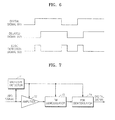
- FIG. 6 is a diagram illustrating examples of signals generated in the edge detector of FIG. 5 .
- FIG. 7 is a block diagram illustrating an example of a receiver of the FM-UWB communication system of FIG. 1 .
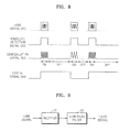
- FIG. 8 is a diagram illustrating an example of a method of demodulating a UWB signal in the receiver of FIG. 7 .
- FIG. 9 is a block diagram illustrating an example of an envelope detector of the receiver of FIG. 7 .
- FIG. 10 is a diagram illustrating examples of signals generated in the envelope detector of FIG. 9 .
- FIG. 11 is a flowchart illustrating an example of a method of modulating a digital signal in the transmitter.
- FIG. 12 is a flowchart illustrating an example of a method of demodulating a UWB signal in the receiver.
- FIG. 1 is a block diagram illustrating an example of a frequency modulation-ultra-wideband (FM-UWB) communication system.
- the FM-UWB communication system includes a transmitter 10 and a receiver 11.
- the transmitter 10 modulates a digital signal into a UWB signal, and transmits the UWB signal.
- the receiver 11 receives the UWB signal, and demodulates the UWB signal into a digital signal.
- the transmitter 10 receives a digital signal, modulates the digital signal into a frequency-shift keying (FSK) modulation signal through FSK modulation, modulates the FSK modulation signal into a UWB signal through FM, and transmits the UWB signal.
- FSK frequency-shift keying
- digital signal refers to data composed of 0 and 1.
- the transmitter 10 includes an FSK modulator ("FSK”) and an FM modulator (“FM MOD").
- the FSK modulator modulates a digital signal into an FSK modulation signal.
- the FSK modulation signal is a signal including a frequency that varies according to the digital signal being 0 and 1.
- the FSK modulator may output a signal including a frequency of 1 MHz when the digital signal is 0, may output a signal including a frequency of 5 MHz when the digital signal is 1, or vice versa.
- the FSK modulation signal is a triangle wave signal in FIG. 1 , the example is not limited thereto, and the FSK modulation signal may be modulated into an analog signal including a waveform other than a triangle wave signal.
- the frequency of the FSK modulation signal varies, a minimum voltage and a maximum voltage of the FSK modulation signal may be maintained to be constant. That is, the FSK modulation signal may include a constant amplitude and the varying frequency. For example, when an amplitude of a FSK modulation signal including a high frequency ranges from 1 volt (V) to 5 V, an amplitude of a FSK modulation signal including a low frequency may also range from 1 V to 5 V.
- the FM modulator modulates the FSK modulation signal into a UWB signal including another waveform according to the frequency of the FSK modulation signal input from the FSK modulator, and outputs the UWB signal, e.g., through an output amplifier ("OA") and an antenna.
- the UWB signal may be a sine wave signal.
- Frequencies of the UWB signal output from the FM modulator and the FSK modulation signal are proportional to each other, and include a linear relationship therebetween.
- the FM modulator outputs the UWB signal whose frequency is linearly increased from 3 GHz to 4 GHz while the triangle wave signal is increased from 1 V to 5 V.
- the frequency of the UWB signal may be more than several hundred times greater than the frequency of the triangle wave signal. Accordingly, more than several hundred cycles of a sine wave signal whose frequency is increased or decreased may be output from the FM modulator for one cycle of a triangle wave signal.
- the receiver 11 receives the UWB signal, e.g., through an antenna and a preamplifier ("PRE AMP"), and demodulates the UWB signal into a digital signal.
- the receiver 11 includes an FM demodulator (“FM DEMOD”) and an FSK demodulator (“FSK DEMOD”).
- FM DEMOD FM demodulator
- FSK DEMOD FSK demodulator
- the FM demodulator outputs a demodulation signal that varies according to the frequency of the UWB signal. That is, the FM demodulator outputs the demodulation signal that is increased when the frequency of the UWB signal input into the FM demodulator is increased, and that is decreased when the frequency of the UWB signal is decreased.
- the FM demodulator may correspond a minimum frequency and a maximum frequency of the UWB signal to respective voltage values, to generate the demodulation signal that varies between the voltage values. For example, if the minimum frequency of the UWB signal input into the FM demodulator is 3 GHz, the maximum frequency of the UWB signal is 4 GHz, a voltage corresponding to the minimum frequency of 3 GHz is 1 V, a voltage corresponding to the maximum frequency of 4 GHz is 5 V, the FM demodulator outputs the demodulation signal that is increased from 1 V to 5 V while the frequency of the UWB signal is changed from 3 GHz to 4 GHz. Also, the FM demodulator outputs the demodulation signal that is decreased from 5 V to 1 V while the frequency of the UWB signal is changed from 4 GHz to 3 GHz.
- the FSK demodulator receives the demodulation signal from the FM demodulator, and outputs a digital signal according to a frequency of the demodulation signal.
- the FSK demodulator discriminates two frequencies, and outputs the digital signal to be 0 when a signal including a low frequency is input, and outputs the digital signal to be 1 when a signal including a high frequency is input. That is, the FSK demodulator outputs a direct current (DC) signal including a low voltage when the frequency of the demodulation signal is low, and outputs a DC signal including a high voltage when the frequency of the demodulation signal is high.
- DC direct current
- FIG. 2 is a diagram illustrating examples of signals modulated in the transmitter 10 of the FM-UWB communication system of FIG. 1 .
- the transmitter 10 modulates a digital signal 21 into a modulation signal 22 including another frequency according to the digital signal 21, and outputs a UWB signal 23 whose frequency varies according to the modulation signal 22.
- the digital signal 21 includes two DC voltages including different levels 0 and 1. A low voltage may be expressed as 0, a high voltage may be expressed as 1, or vice versa.
- the modulation signal 22 is a signal whose frequency varies according to the digital signal 21.
- the modulation signal 22 is a triangle wave signal including a low frequency when the digital signal 21 includes the low voltage, and is a triangle wave signal including a high frequency when the digital signal 21 includes the high voltage. That is, the modulation signal 22 is a triangle wave signal including two frequencies and one amplitude.
- the UWB signal 23 is a signal generated by modulating the modulation signal 22 that is a triangle wave signal into a sine wave signal including a wide frequency band. That is, the UWB signal 23 is a sine wave signal whose frequency is increased when the modulation signal 22 is increased in voltage, and is decreased when the modulation signal 22 is decreased in voltage. Accordingly, the frequency of the UWB signal 23 is increased and decreased for one cycle of the modulation signal 22. Since the frequency of the UWB signal 23 is more than 10 times greater than the frequency of the modulation signal 22, more than 10 cycles of the UWB signal 23 is generated for one cycle of the modulation signal 22. The frequency of the UWB signal 23 is rapidly changed when the modulation signal 22 is rapidly changed in voltage.
- the frequency of the UWB signal 23 is slowly changed when the modulation signal 22 is slowly changed in voltage.
- a frequency band of the UWB signal 23 is previously set, and the frequency of the UWB signal 23 is repeatedly increased and decreased in the preset frequency band.
- the UWB signal 23 generated for one cycle of the modulation signal 22 is shown in FIG. 2 .
- FIG. 3 is a block diagram illustrating an example of the transmitter 10.
- the transmitter 10 includes an edge detector 31, an FSK modulator 32, an FM modulator 33, and an amplifier 34.
- the edge detector 31 receives a digital signal indicating data to be transmitted, and generates and outputs a pulse signal when each of edges of the digital is received. That is, the edge detector 31 outputs the pulse signal when the digital signal is changed.
- the edge detector 31 may output the pulse signal when the digital signal is changed from 0 to 1 and/or from 1 to 0.
- the edge detector 31 may be a circuit including an XOR logic gate and a time delay unit. The time delay unit delays the digital signal by a predetermined period of time to generate a delayed digital signal, and outputs the delayed digital signal to the XOR logic gate.
- the XOR logic gate receives the digital signal that is not delayed (referred to as a non-delayed digital signal) and the delayed digital signal, and outputs 1 when only one of the non-delayed digital signal and the delayed digital signal is 1. Accordingly, the XOR logic gate outputs 1 corresponding to the delayed digital signal when the digital signal is changed. That is, the XOR logic gate outputs the pulse signal during the delayed period of time.
- the edge detector 31 is not limited thereto, and may be any of various circuits.
- the edge detector 31 may output the pulse signal to the FSK modulator 32, the FM modulator 33, and/or the amplifier 34.
- the pulse signal output from the edge detector 31 may be used to control an operation time of the FSK modulator 32, the FM modulator 33, and/or the amplifier 34. That is, a power supply to the FSK modulator 32, the FM modulator 33, and/or the amplifier 34 may be continued when the FSK modulator 32, the FM modulator 33, and/or the amplifier 34 receive the pulse signal from the edge detector 31.
- the power supply to the FSK modulator 32, the FM modulator 33, and/or the amplifier 34 may be cut off when the FSK modulator 32, the FM modulator 33, and/or the amplifier 34 does not receive the pulse signal from the edge detector 31, thereby reducing unnecessary power consumption.
- the edge detector 31 outputs the pulse signal to the FSK modulator 32, the FM modulator 33, and the amplifier 34 in FIG. 3 , the example is not limited thereto, and the edge detector 31 may output the pulse signal to any one of the FM modulator 33, the FSK modulator 32, and the amplifier 34.
- the FSK modulator 32 receives the digital signal, and modulates the digital signal into another frequency based on a value of the digital signal, to generate and output a modulation signal.
- the FSK modulator 32 outputs a triangle wave signal including a low frequency when the digital signal input into the FSK modulator 32 includes a low voltage, and outputs a triangle wave signal including a high frequency when the digital signal input into the FSK modulator 32 includes a high voltage.
- the FSK modulator 32 may be supplied with power to operate only when the FSK modulator 32 receives the pulse signal from the edge detector 31. Accordingly, the power supply to the FSK modulator 32 may be cut off when the FSK modulator 32 does not receive the pulse signal from the edge detector 31, thereby reducing unnecessary power consumption.
- the FM modulator 33 receives the modulation signal from the FSK modulator 32, and modulates the modulation signal into another waveform based on a frequency of the modulation signal, to generate and output a signal.
- the signal generated from the FM modulator 33 is a UWB signal generated over a wide frequency band.
- the FM modulator 33 may generate a UWB signal whose bandwidth varies from 3 GHz to 4 GHz based on the modulation signal received from the FSK modulator 32.
- the FM modulator 33 may be supplied with power to operate only when the FM modulator 33 receives the pulse signal from the edge detector 31. Accordingly, the power supply to the FM modulator 33 may be cut off when the FM modulator 33 does not receive the pulse signal from the edge detector 31.
- the FM modulator 33 does not need to generate the UWB signal for all signals received from the FSK modulator 32. Since the FM modulator 33 may operate only when the FM modulator 33 receives the pulse signal from the edge detector 31, the FM modulator 33 does not operate for an unnecessary period of time, thereby reducing power consumption.
- a triangle wave signal is repeatedly input into the FM modulator 33 from the FSK modulator 32. Since the triangle wave signal is repeatedly input into the FM modulator 33 from the FSK modulator 32, although the triangle wave signal is shown to be input for only one cycle, the triangle wave signal is also input for other cycles.
- FIG. 4 is a diagram illustrating an example of a method of modulating a digital signal 41 into a UWB signal 44 in the transmitter 10 of FIG. 3 .
- the transmitter 10 modulates the digital signal 41 into a modulation signal 43, and generates an edge detection signal 42 including pulse signals generated when the digital signal 41 is changed.
- the digital signal 41 includes two DC voltages including different levels 0 and 1. A low voltage may be expressed as 0, a high voltage may be expressed as 1, or vice versa. The digital signal 41 indicates data to be transmitted.
- the edge detection signal 42 includes pulse signals generated when the digital signal 41 is changed. That is, the edge detection signal 42 includes the pulse signals generated when the digital signal 41 is changed from the low voltage to the high voltage, and/or from the high voltage to the low voltage.
- the edge detection signal 42 may be generated by inputting the digital signal 41 and a delayed digital signal passing through the time delay unit into the XOR logic gate.
- the XOR logic gate outputs 1 when the digital signal 41 and the delayed digital signal include different voltages, and outputs 0 when the digital signal 41 and the delayed digital signal include the same voltage. Accordingly, when the digital signal 41 and the delayed digital signal are input into the XOR logic gate and the digital signal 41 is changed, since the digital signal 41 is different than the delayed digital signal by as much as a predetermined period of time, the XOR logic gate outputs 1.
- the modulation signal 43 is generated by modulating the digital signal 41 through FM.
- the modulation signal 43 is a triangle wave signal including a low frequency when the digital signal 41 includes the low voltage, is a triangle wave signal including a high frequency when the digital signal 41 includes the high voltage, or vice versa.
- the UWB signal 44 is generated by modulating the modulation signal 43.
- the modulation signal 43 is a triangle wave signal modulated into the UWB signal 44 that is a sine wave signal including a wide frequency band.
- the UWB signal 44 is a sine wave signal whose frequency is increased when the modulation signal 43 is increased in voltage, and is a sine wave signal whose frequency is decreased when the modulation signal 43 is decreased in voltage. Accordingly, a frequency of the UWB signal 44 is increased and decreased for one cycle of the modulation signal 43.
- the frequency of the UWB signal 44 is rapidly changed when the modulation signal 43 is rapidly changed, and is slowly changed when the modulation signal 43 is slowly changed.
- a frequency band of the UWB signal 44 is previously set, and the frequency of the UWB signal 44 is repeatedly increased and decreased in the preset frequency band.
- the frequency of the UWB signal 44 may be more than several hundred times greater than a frequency of the modulation signal 43. Accordingly, more than 10 cycles of the UWB signal 44 may be generated for one cycle of the modulation signal 43.
- the UWB signal 44 generated for one cycle of the modulation signal 43 is shown in FIG. 4 , and the UWB signal 44 generated for other cycles are not shown.
- the UWB signal 44 is generated only when a pulse signal of the edge detection signal 42 is generated. Accordingly, since the UWB signal 44 is not generated when a pulse signal of the edge detection signal 42 is not generated, power consumption of the transmitter 10 may be further reduced than when the UWB signal 44 is generated continuously. Periods of time when the UWB signal 44 is generated and is not generated are indicated by ON and OFF, respectively, in FIG. 4 .
- FIG. 5 is a block diagram illustrating an example of the edge detector 31 of the transmitter 10 of FIG. 3 .
- the edge detector 31 includes a time delay unit 51 and an XOR logic gate 52.
- the edge detector 31 receives a digital signal indicating data to be transmitted, and generates and outputs a pulse signal ("an edge detection signal") when each of edges of the digital signal is received.
- the time delay unit 51 delays the digital signal input thereto by a predetermined period of time to generate a delayed digital signal, and outputs the delayed digital signal to the XOR logic gate 52.
- the XOR logic gate 52 receives the digital signal and the delayed digital signal, and outputs a constant voltage value (e.g., 1) when the digital signal and the delayed digital signal include different voltages. Accordingly, when the digital signal is changed, since the digital signal is different than the delayed digital signal by as much as the predetermined period of time, the edge detector 31 outputs the pulse signal including the constant voltage value during the delayed period of time.
- a constant voltage value e.g., 1
- edge detector 31 of FIG. 3 is shown in FIG. 5 , the example is not limited thereto. It will be understood by one of ordinary skill in the art that the edge detector 31 may be constructed in various other ways.
- FIG. 6 is a diagram illustrating examples of signals generated in the edge detector 31 of FIG. 5 .
- the edge detector 31 generates and outputs an edge detection signal 63 based on a digital signal 61 and a delayed signal 62.
- the time delay unit 51 of the edge detector 31 delays the digital signal 61 by a predetermined period of time to generate and output the delayed signal 62.
- the delayed signal 62 is the same as the digital signal 61 except that the delayed signal 62 is delayed from the digital signal 61.
- the edge detection signal 63 includes a constant voltage value (e.g., 1) when the digital signal 61 and the delayed signal 62 include different values.
- the edge detector 31 generates and outputs a pulse signal when the digital signal 61 is changed.
- both the digital signal 61 and the delayed signal 62 include the same value (e.g., 1 or 0)
- the edge detector 31 outputs 0, and when only one of the digital signal 61 and the delayed signal 62 includes 1, the edge detector 31 outputs 1.
- FIG. 7 is a block diagram illustrating an example of the receiver 11 of the FM-UWB communication system of FIG. 1 .
- the receiver 11 includes an envelope detector 71, an amplifier 72, an FM demodulator 73, and an FSK demodulator 74.
- the envelope detector 71 receives a UWB signal, and generates and outputs a pulse signal based on the received UWB signal to control operations of the amplifier 72, the FM demodulator 73, and/or the FSK demodulator 74.
- the amplifier 72, the FM demodulator 73, and/or the FSK demodulator 74 may operate only when the amplifier 72, the FM demodulator 73, and/or the FSK demodulator 74 receive the pulse signal from the envelope detector 71, thereby reducing power consumed by the amplifier 72, the FM demodulator 73, and/or the FSK demodulator 74.
- the receiver 11 may control the amplifier 72, the FM demodulator 73, and/or the FSK demodulator 74 to operate only when the amplifier 72, the FM demodulator 73, and/or the FSK demodulator 74 receive the pulse signal from the envelope detector 71.
- the receiver 11 may further cut off power supply to the amplifier 72, the FM demodulator 73, and/or the FSK demodulator 74 when the amplifier 72, the FM demodulator 73, and/or the FSK demodulator 74 do not receive the pulse signal, thereby reducing power consumed by the amplifier 72, the FM demodulator 73, and/or the FSK demodulator 74.
- the envelope detector 71 outputs the pulse signal to the amplifier 72, the FM demodulator 73, and the FSK demodulator 74 in FIG. 7
- the envelope detector 71 may output the pulse signal to any one of the amplifier 72, the FM demodulator 73, and the FSK demodulator 74.
- the envelope detector 71 detects an envelope of the UWB signal during periods of time when the UWB signal is received by the envelope detector 71.
- the envelope contacts all ripples of the UWB signal.
- the envelope is a curve that contacts all waves of the sine wave signal.
- the envelope may be a straight line.
- the UWB signal is transmitted from the transmitter 10 of FIG. 3 .
- the UWB signal is generated in the FM modulator 33 only during periods of time when the edge detector 31 generates and outputs a pulse signal. Since the FM modulator 33 generates the UWB signal only when the edge detector 31 outputs the pulse signal, the UWB signal received by the receiver 11 of FIG. 7 is received during some periods of time and is not received during other periods of time. Accordingly, the envelope of the UWB signal is the pulse signal during the periods of time when the UWB signal is received.
- the envelope detector 71 outputs the envelope, which is the pulse signal, to the amplifier 72, the FM demodulator 73, and/or the FSK demodulator 74.
- the pulse signal output from the envelope detector 71 during the periods of time when the UWB signal is received may be referred to as an envelope detection signal. Accordingly, the envelope detector 71 does not output any signal during the other periods of times when the UWB signal is not received.
- the FM demodulator 73 receives a UWB signal from the amplifier 72 amplifying the UWB signal, and demodulates the UWB signal into another frequency based on a waveform of the UWB signal, to generate and output a demodulated UWB signal.
- the FM demodulator 73 may operate only when the FM demodulator 73 receives the pulse signal from the envelope detector 71. Accordingly, since the pulse signal is output from the envelope detector 71 only during the periods of time when the UWB signal is received, the FM demodulator 73 operates only when the UWB signal is received.
- the FM demodulator 73 receives the UWB signal, and outputs the demodulated UWB signal proportional to a frequency of the UWB signal.
- the UWB signal input into the FM demodulator 73 may be a sine wave signal whose frequency is repeatedly increased and decreased.
- the FM demodulator 73 outputs a signal that is increased in voltage when the frequency of the UWB signal is increased, and outputs a signal that is decreased in voltage when the frequency of the UWB signal is decreased.
- the FM demodulator 73 previously sets a width corresponding to a variation range of the frequency of the UWB signal, and outputs a signal varying in the width.
- the frequency of the UWB signal is repeatedly increased and decreased.
- the FM demodulator 73 When a speed at which the frequency of the UWB signal is changed is high, the FM demodulator 73 outputs a signal including a high frequency, and when a speed at which the frequency of the UWB signal is changed is low, the FM demodulator 73 outputs a signal including a low frequency.
- the FSK demodulator 74 receives the demodulated UWB signal from the FM demodulator 73, demodulates the demodulated UWB signal into a digital signal based on a frequency of the demodulated UWB signal, and outputs the digital signal.
- the digital signal is changed in voltage value when the frequency of the demodulated UWB signal is changed. That is, when the frequency of the demodulation signal is a high frequency, the FSK demodulator 74 outputs a signal including a high DC voltage, and when the frequency of the demodulation signal is a low frequency, the FSK demodulator 74 outputs a signal including a low DC voltage.
- the signal including the high DC voltage may be a digital signal including a voltage expressed as 1
- the signal including the low DC voltage may be a digital signal including a voltage expressed as 0.
- FIG. 8 is a diagram illustrating an example of a method of demodulating a UWB signal 81 in the receiver 11 of FIG. 7 .
- a frequency of the UWB signal 81 is increased and decreased in a frequency band for a predetermined period of time.
- the UWB signal 81 is generated for one cycle of a demodulation signal 83, and the frequency of the UWB signal 81 may be more than 10 times greater than a frequency of the demodulation signal 83.
- An envelope detection signal 82 is a curve contacting all ripples of the UWB signal 81.
- the envelope detection signal 82 is a pulse signal including a constant amplitude while the UWB signal 81 is received in the receiver 11.
- the demodulation signal 83 is a triangle wave signal varying based on the frequency of the UWB signal 81.
- the demodulation signal 83 is increased in voltage when the frequency of the UWB signal 81 is increased, and is decreased in voltage when the frequency of the UWB signal 81 is decreased.
- the demodulation signal 83 is a triangle wave signal including a high frequency when the frequency of the UWB signal 81 is rapidly changed, and is a triangle wave signal including a low frequency when the frequency of the UWB signal 81 is slowly changed.
- the demodulation signal 83 is generated only when the UWB signal 81 is received.
- a digital signal 84 includes a value varying based on a frequency of the demodulation signal 83.
- the digital signal 84 includes a large value when the frequency of the demodulation signal 83 is high, and includes a small value when the frequency of the demodulation signal 83 is low.
- the value of the digital signal 84 is maintained when there is no demodulation signal 83.
- FIG. 9 is a block diagram illustrating an example of the envelope detector 71 of the receiver 11 of FIG. 7 .
- the envelope detector 71 includes a rectifier 91 and a low-pass filter 92.
- the envelope detector 71 receives a UWB signal, and generates and outputs a pulse signal (i.e., an envelope detection signal) only during periods of time when the UWB signal is received.
- a pulse signal i.e., an envelope detection signal
- the rectifier 91 receives the UWB signal, rectifies the UWB signal to generate a rectified signal, and outputs the rectified signal to the low-pass filter 92.
- the rectifier 91 rectifies the UWB signal in such a manner that components of the UWB signal under a reference line are moved upward to be located over the reference line, and thus, components are only allowed to be located over the reference line..
- the low-pass filter 92 passes only a low-frequency component of the rectified signal. Accordingly, the low-pass filter 92 outputs the pulse signal, which is the rectified signal without a high-frequency component and is a DC signal generated while the UWB signal is received.
- the envelope detector 71 is shown in FIG. 9 , the example is not limited thereto. It will be understood by one of ordinary skill in the art that the envelope detector 71 of FIG. 9 may be constructed in various other ways.
- FIG. 10 is a diagram illustrating examples of signals generated in the envelope detector 71 of FIG. 9 .
- a UWB signal 110 input into the envelope detector 71 is a sine wave signal whose frequency varies, and includes periods of time when the sine wave signal exists and other periods of time when the sine wave signal does not exist. Since the UWB signal 110 is output from the transmitter 10 of FIG. 3 , the UWB signal 110 includes the periods of time when the sine wave signal exists and the other periods of time when the sine wave signal does not exist based on a pulse signal output from the edge detector 31.
- the frequency of the UWB signal 110 varies in a frequency band. In this example, the frequency band is previously set. Also, a speed at which the frequency of the UWB signal 110 is changed varies. That is, the frequency of the UWB signal 110 is rapidly changed during some periods of time, and is slowly changed in other periods of time.
- a rectified signal 111 output from the rectifier 91 is generated by moving upward components of the UWB signal 110 under a reference line to be located over the reference line, and thus, allowing components to be located only over the reference line. Accordingly, half-period signals of the sine wave signal are located only over the reference line.
- An envelope detection signal 112 output from the low-pass filter 92 is generated by passing only a low-frequency component from among frequency components of the rectified signal 111. Accordingly, the envelope detection signal 112 is a pulse signal close to a DC signal. As shown in FIG. 9 , the envelope detection signal 112 is generated by passing the rectified signal 111 through the low-pass filter 92. Referring again to FIG. 10 , the envelope detection signal 112 is a line contacting all ripples of the rectified signal 111.
- FIG. 11 is a flowchart illustrating an example of a method of modulating a digital signal in the transmitter 10.
- the method includes operations sequentially performed by the transmitter 10 of FIG. 3 . Accordingly, although omitted, the description given with reference to the transmitter 10 applies to the method of FIG. 11 .
- the method of FIG. 11 includes the following operations.
- the edge detector 31 of the transmitter 10 receives the digital signal, and generates and outputs a pulse signal when each of edges of a digital signal indicating data to be transmitted is detected or received by the edge detector 31.
- the digital signal includes a high voltage and a low voltage. An edge of the digital signal indicates that the digital signal is changed from the high voltage to the low voltage, or from the low voltage to the high voltage.
- the edge detector 31 detects the edges of the digital signal, and generates and outputs the pulse signal when each of the edges of the digital signal is detected. The method of detecting the edges of the digital signal in the edge detector 31 has already been described in detail with reference to FIG. 5 .
- the pulse signal is output to the FSK modulator 32, the FM modulator 33, and/or the amplifier 34 to enable the FSK modulator 32, the FM modulator 33, and/or the amplifier 34 to operate.
- the FSK modulator 32 of the transmitter 10 receives the digital signal, and modulates the digital signal into a modulation signal based on a value of the digital signal to output the modulation signal.
- the FSK modulator 32 generates the modulation signal including a frequency that is previously set based on a voltage of the digital signal. That is, when the voltage of the digital signal is a low voltage, the FSK modulator 32 may generate the modulation signal to include a low frequency, when the voltage of the digital signal is a high voltage, the FSK modulator 32 may generate the modulation signal to include a high frequency, or vice versa.
- the low frequency and the high frequency are previously determined.
- the low frequency may be 1 MHz
- the high frequency may be 5 MHz.
- the FM modulator 33 of the transmitter 10 receives the modulation signal from the FSK modulator 32, and modulates the modulation signal into a UWB signal based on a frequency of the modulation signal to output the UWB signal.
- the FM modulator 33 modulates the modulation signal only during periods of time when the FM modulator 33 receives the pulse signal from the edge detector 31, i.e., when the pulse signal is generated. Accordingly, since the FM modulator 33 does not operate when the FM modulator 33 does not receive the pulse signal, power consumption may be reduced compared to a case where the FM modulator 33 operates continuously.
- the modulation signal received from the FM modulator 33 includes periods of time when the modulation signal is rapidly and slowly, repeatedly increased and decreased in voltage.
- the FM modulator 33 may generate and output a sine wave signal whose frequency is increased when the modulation signal is increased in voltage, and is decreased when the modulation signal is decreased in voltage. Since a speed at which the modulation signal is repeatedly increased and decreased in voltage is changed, a speed at which the frequency of the signal output from the FM modulator 33 is increased and decreased is also changed accordingly.
- FIG. 12 is a flowchart illustrating an example of a method of demodulating a UWB signal in the receiver 11.
- the method includes operations sequentially performed by the receiver 11 of FIG. 3 . Accordingly, although omitted, the description given with reference to the receiver 11 applies to the method of FIG. 12 .
- the method of FIG. 12 includes the following operations.
- the envelope detector 71 of the receiver 11 receives a UWB signal from the transmitter 10, and generates and outputs a pulse signal when an envelope of the UWB signal is detected or received by the envelope detector 71.
- the envelope is a curve contacting all ripples of the UWB signal.
- the UWB signal is a sine wave signal
- the envelope may be a straight line contacting all waves of the sine wave signal. Accordingly, the pulse signal may be close to a DC signal. Since the UWB signal is output from the transmitter 10 only when a pulse signal is generated by the edge detector 31 of the transmitter 10, the UWB signal may be received during some periods of time, and may not be received during other periods of time.
- the pulse signal output from the envelop detector 71 may be output during the periods of time when the UWB signal is received, and may not be received during the other periods of time when the UWB signal is not received.
- the method of detecting the envelope of the UWB signal in the envelope detector 71 has already been described in detail with reference to FIG. 9 .
- the FM demodulator 73 of the receiver 11 receives the UWB signal from the transmitter 10, and demodulates the UWB signal into a demodulation signal based on a frequency of the UWB signal to output the demodulation signal.
- the FM demodulator 73 demodulates the UWB signal only during periods of time when the FM demodulator 73 receives the pulse signal from the envelope detector 71, i.e., when the pulse signal is generated. Accordingly, since the FM demodulator 73 does not operate when the FM demodulator 73 does not receive the pulse signal (since power supply to the FM demodulator 73 is cut off), power consumed by the FM demodulator 73 may be reduced compared to a case where the FM demodulator 73 operates continuously.
- the FM demodulator 73 generates and outputs the demodulation signal proportional to a frequency of the UWB signal.
- an amplitude of the demodulation signal is previously set in a variation range based on the frequency of the UWB signal.
- the FM demodulator 73 may generate and output the demodulation signal to be increased in voltage when the frequency of the UWB signal is increased, and to be decreased in voltage when the frequency of the UWB signal is decreased.
- the demodulation signal may be previously set to be changed from 0 V to 5 V.
- the FSK demodulator 74 of the receiver 11 demodulates the demodulation signal into a digital signal based on a frequency of the demodulation signal to output the digital signal.
- the digital signal is a DC signal including a high voltage and a low voltage.
- the FSK demodulator 74 outputs the DC signal to include the high voltage when the demodulation signal includes a high frequency, and outputs the DC signal to include the low voltage when the demodulation signal includes a low frequency.
- a transmitter and a receiver which may reduce power consumption by generating a pulse signal and controlling modulators and demodulators to operate only when such modulators and demodulators receive the pulse signal.
- the units described herein may be implemented using hardware components and software components.
- the hardware components may include microphones, amplifiers, band-pass filters, audio to digital convertors, and processing devices.
- a processing device may be implemented using one or more general-purpose or special purpose computers, such as, for example, a processor, a controller and an arithmetic logic unit, a digital signal processor, a microcomputer, a field programmable array, a programmable logic unit, a microprocessor or any other device capable of responding to and executing instructions in a defined manner.
- the processing device may run an operating system (OS) and one or more software applications that run on the OS.
- the processing device also may access, store, manipulate, process, and create data in response to execution of the software.
- OS operating system
- a processing device may include multiple processing elements and multiple types of processing elements.
- a processing device may include multiple processors or a processor and a controller.
- different processing configurations are possible, such a parallel processors.
- the software may include a computer program, a piece of code, an instruction, or some combination thereof, to independently or collectively instruct or configure the processing device to operate as desired.
- Software and data may be embodied permanently or temporarily in any type of machine, component, physical or virtual equipment, computer storage medium or device, or in a propagated signal wave capable of providing instructions or data to or being interpreted by the processing device.
- the software also may be distributed over network coupled computer systems so that the software is stored and executed in a distributed fashion.
- the software and data may be stored by one or more computer readable recording mediums.
- the computer readable recording medium may include any data storage device that can store data which can be thereafter read by a computer system or processing device.
- non-transitory computer readable recording medium examples include read-only memory (ROM), random-access memory (RAM), CD-ROMs, magnetic tapes, floppy disks, optical data storage devices.
- ROM read-only memory
- RAM random-access memory
- CD-ROMs compact disc-read only memory
- magnetic tapes magnetic tapes
- floppy disks optical data storage devices.
- functional programs, codes, and code segments accomplishing the examples disclosed herein can be easily construed by programmers skilled in the art to which the examples pertain based on and using the flow diagrams and block diagrams of the figures and their corresponding descriptions as provided herein.
Landscapes
- Engineering & Computer Science (AREA)
- Computer Networks & Wireless Communication (AREA)
- Signal Processing (AREA)
- Digital Transmission Methods That Use Modulated Carrier Waves (AREA)
- Transmitters (AREA)
- Circuits Of Receivers In General (AREA)
Abstract
Description
- The following description relates to transmitters and receivers in frequency modulation-ultra-wideband (FM-UWB) communication systems.
- Ultra-wideband (UWB) has drawn attention as a very promising technology in the fields of wireless communications, imaging, and sensors, as its capabilities of transmitting multimedia data at a high speed of hundreds of megabits per second (Mbps) to 1 gigabit per second (Gbps) and of detecting a precise location are highlighted. As UWB has been permitted for commercial use in the field of wireless communications, various attempts have been made to use UWB in short-range wireless personal area networks.
- The Federal Communications Commission in the United States has defined UWB as a wireless communication technology including a spectrum that occupies a bandwidth greater than or equal to 20% of a center frequency, or a bandwidth of at least 500 megahertz (MHz). Accordingly, existing carrier modulation including a spectrum that occupies a bandwidth of at least 500 MHz may be considered as UWB. In general, UWB is regarded as a low-power, high-speed, short-range wireless communication technology that may perform communication in a range from 3.1 to 10.6 gigahertz (GHz) at a rate of 100 Mbps or more over a band wider than that of a conventional communication technology. UWB uses an extremely wide band, and requires relatively low power. A UWB system is based on a lower power spectral density over a very wide frequency band than that of a conventional narrowband system or a wideband code division multiple access (CDMA) system. Since the UWB system spreads and transmits a signal over a bandwidth of several GHz in order to prevent interference with another communication system, the UWB system may provide communications without interfering with another narrowband signal and without being greatly affected by a frequency. As a result, the UWB system may share a frequency spectrum and require very low power. UWB has been studied in Institute of Electrical and Electronics Engineers (IEEE) 802.15.3a, which is a UWB standard for a wireless personal area network (WPAN), and in IEEE 802.15.4A, which is a UWB standard for a low-rate and low-power WPAN including a wireless positioning function.
- Unlike a conventional wireless communication system using a continuous sine wave signal, an impulse radio (IR)-UWB system includes a transmitter that discontinuously transmits a Gaussian monocycle pulse or a pulse with a narrow width of 1 nanosecond (ns) or so. Accordingly, the IR-UWB system may transmit a signal using a much wider band (hundreds of MHz to several GHz) than a data modulation band, and thus, may greatly reduce a power spectral density, thereby reducing interference. Also, since the IR-UWB system uses such a pulse, the IR-UWB system is very resilient to multi-path fading. Unlike a conventional wireless communication system that puts a signal to be transmitted on a carrier, performs upward modulation and amplification of the signal, and transmits the modulated and amplified signal, the IR-UWB system modulates a baseband signal into an impulse signal, and directly transmits the impulse signal. Accordingly, the IR-UWB system may be simply constructed at low cost.
- In one general aspect, there is provided a transmitter including a detector configured to generate a pulse signal when an edge of a digital signal is detected. The transmitter further includes a first modulator configured to modulate the digital signal into a first modulation signal based on a value of the digital signal. The transmitter further includes a second modulator configured to modulate the first modulation signal into a second modulation signal based on a frequency of the first modulation signal when the pulse signal is generated.
- The second modulator may be further configured to be cut off from a power supply when the pulse signal is not generated.
- The first modulator may be further configured to output the first modulation signal when the pulse signal is generated.
- The first modulator may be further configured to be cut off from a power supply when the pulse signal is not generated.
- The transmitter may further include an amplifier configured to amplify the second modulation signal when the pulse signal is generated.
- The transmitter may further include an amplifier configured to amplify the second modulation signal, and be cut off from a power supply when the pulse signal is not generated.
- The detector may include a time delay unit configured to delay the digital signal by a predetermined period of time to generate a delayed signal. The detector may further include an XOR gate configured to not output the pulse signal when the digital signal and the delayed signal include the same voltage, and output the pulse signal when the digital signal and the delayed signal include different voltages.
- In another general aspect, there is provided a receiver including a detector configured to generate a pulse signal when an envelope of an input signal is detected. The receiver further includes a first demodulator configured to demodulate the input signal into a demodulation signal based on a waveform of the input signal when the pulse signal is generated. The receiver further includes a second demodulator configured to demodulate the demodulation signal into a digital signal based on a frequency of the demodulation signal.
- The first demodulator may be further configured to be cut off from a power supply when the pulse signal is not generated.
- The second demodulator may be further configured to output the digital signal when the pulse signal is generated.
- The second demodulator may be further configured to be cut off from a power supply when the pulse signal is not generated.
- The receiver may further include an amplifier configured to amplify the input signal when the pulse signal is generated.
- The receiver may further include an amplifier configured to amplify the input signal, and be cut off from a power supply when the pulse signal is not generated.
- The detector may include a rectifier configured to rectify the input signal. The detector may further include a low-pass filter configured to pass a low-frequency component of the rectified input signal to generate the pulse signal.
- In still another general aspect, there is provided a transmitting method including generating a pulse signal when an edge of a digital signal is detected. The transmitting method further includes modulating the digital signal into a first modulation signal based on a value of the digital signal. The transmitting method further includes modulating the first modulation signal into a second modulation signal based on a frequency of the first modulation signal when the pulse signal is generated.
- The transmitting method may further include determining the frequency of the first modulation signal based on the value of the digital signal. The transmitting method may further include determining a waveform of the second modulation signal based on the frequency of the first modulation signal, the second modulation signal being a ultra-wideband (UWB) signal.
- In yet another general aspect, there is provided a receiving method including generating a pulse signal when an envelope of an input signal is detected. The receiving method further includes demodulating the input signal into a demodulation signal based on a waveform of the input signal when the pulse signal is generated. The receiving method further includes demodulating the demodulation signal into a digital signal based on a frequency of the demodulation signal.
- The receiving method may further include determining the frequency of the demodulation signal based on the waveform of the input signal, the input signal being a ultra-wideband (UWB) signal. The receiving method may further include determining a value of the digital signal based on the frequency of the demodulation signal.
- In another general aspect, there is provided a computer-readable storage medium storing a program including instructions to cause a computer to generate a pulse signal based on a digital signal. The computer is further caused to modulate the digital signal into a modulation signal. The computer is further caused to modulate the modulation signal into an output signal based on the pulse signal.
- The computer may be further caused to modulate the modulation signal into the output signal when the pulse signal is generated.
- Other features and aspects may be apparent from the following detailed description, the drawings, and the claims.
- These and/or other aspects will become apparent and more readily appreciated from the following description of the examples, taken in conjunction with the accompanying drawings.
-
FIG. 1 is a block diagram illustrating an example of a frequency modulation-ultra-wideband (FM-UWB) communication system. -
FIG. 2 is a diagram illustrating examples of signals modulated in a transmitter of the FM-UWB communication system ofFIG. 1 . -
FIG. 3 is a block diagram illustrating an example of the transmitter. -
FIG. 4 is a diagram illustrating an example of a method of modulating a digital signal into a UWB signal in the transmitter ofFIG. 3 . -
FIG. 5 is a block diagram illustrating an example of an edge detector of the transmitter ofFIG. 3 . -
FIG. 6 is a diagram illustrating examples of signals generated in the edge detector ofFIG. 5 . -
FIG. 7 is a block diagram illustrating an example of a receiver of the FM-UWB communication system ofFIG. 1 . -
FIG. 8 is a diagram illustrating an example of a method of demodulating a UWB signal in the receiver ofFIG. 7 . -
FIG. 9 is a block diagram illustrating an example of an envelope detector of the receiver ofFIG. 7 . -
FIG. 10 is a diagram illustrating examples of signals generated in the envelope detector ofFIG. 9 . -
FIG. 11 is a flowchart illustrating an example of a method of modulating a digital signal in the transmitter. -
FIG. 12 is a flowchart illustrating an example of a method of demodulating a UWB signal in the receiver. - Throughout the drawings and the detailed description, unless otherwise described, the same drawing reference numerals will be understood to refer to the same elements, features, and structures. The relative size and depiction of these elements may be exaggerated for clarity, illustration, and convenience.
- As used herein, the term "and/or" includes any and all combinations of one or more of the associated listed items.
- The following detailed description is provided to assist the reader in gaining a comprehensive understanding of the methods, apparatuses, and/or systems described herein. Accordingly, various changes, modifications, and equivalents of the systems, apparatuses and/or methods described herein will be suggested to those of ordinary skill in the art. Also, descriptions of well-known functions and constructions may be omitted for increased clarity and conciseness.
-
FIG. 1 is a block diagram illustrating an example of a frequency modulation-ultra-wideband (FM-UWB) communication system. Referring toFIG. 1 , the FM-UWB communication system includes atransmitter 10 and areceiver 11. Thetransmitter 10 modulates a digital signal into a UWB signal, and transmits the UWB signal. Thereceiver 11 receives the UWB signal, and demodulates the UWB signal into a digital signal. - In more detail, the
transmitter 10 receives a digital signal, modulates the digital signal into a frequency-shift keying (FSK) modulation signal through FSK modulation, modulates the FSK modulation signal into a UWB signal through FM, and transmits the UWB signal. The term "digital signal" refers to data composed of 0 and 1. - The
transmitter 10 includes an FSK modulator ("FSK") and an FM modulator ("FM MOD"). The FSK modulator modulates a digital signal into an FSK modulation signal. The FSK modulation signal is a signal including a frequency that varies according to the digital signal being 0 and 1. For example, the FSK modulator may output a signal including a frequency of 1 MHz when the digital signal is 0, may output a signal including a frequency of 5 MHz when the digital signal is 1, or vice versa. Although the FSK modulation signal is a triangle wave signal inFIG. 1 , the example is not limited thereto, and the FSK modulation signal may be modulated into an analog signal including a waveform other than a triangle wave signal. While the frequency of the FSK modulation signal varies, a minimum voltage and a maximum voltage of the FSK modulation signal may be maintained to be constant. That is, the FSK modulation signal may include a constant amplitude and the varying frequency. For example, when an amplitude of a FSK modulation signal including a high frequency ranges from 1 volt (V) to 5 V, an amplitude of a FSK modulation signal including a low frequency may also range from 1 V to 5 V. - The FM modulator modulates the FSK modulation signal into a UWB signal including another waveform according to the frequency of the FSK modulation signal input from the FSK modulator, and outputs the UWB signal, e.g., through an output amplifier ("OA") and an antenna. The UWB signal may be a sine wave signal. When a triangle wave signal is input into the FM modulator, a frequency of the UWB signal output from the FM modulator is increased in sections where the triangle wave signal is increased, and is decreased in sections where the triangle wave signal is decreased. Accordingly, when the FSK modulation signal is rapidly increased or decreased, the frequency of the UWB signal output from the FM modulator is rapidly changed, and when the FSK modulation signal is slowly increased or decreased, the frequency of the UWB signal output from the FM modulator is slowly changed. Frequencies of the UWB signal output from the FM modulator and the FSK modulation signal are proportional to each other, and include a linear relationship therebetween. For example, if the FSK modulation signal is a triangle wave signal, a minimum voltage of the triangle wave signal is 1 V, a maximum voltage of the triangle wave signal is 5 V, a frequency corresponding to the minimum voltage of 1 V is 3 GHz, and a frequency corresponding to the maximum voltage of 5 V is 4 GHz, the FM modulator outputs the UWB signal whose frequency is linearly increased from 3 GHz to 4 GHz while the triangle wave signal is increased from 1 V to 5 V. In this example, the frequency of the UWB signal may be more than several hundred times greater than the frequency of the triangle wave signal. Accordingly, more than several hundred cycles of a sine wave signal whose frequency is increased or decreased may be output from the FM modulator for one cycle of a triangle wave signal.
- The
receiver 11 receives the UWB signal, e.g., through an antenna and a preamplifier ("PRE AMP"), and demodulates the UWB signal into a digital signal. Thereceiver 11 includes an FM demodulator ("FM DEMOD") and an FSK demodulator ("FSK DEMOD"). The FM demodulator outputs a demodulation signal that varies according to the frequency of the UWB signal. That is, the FM demodulator outputs the demodulation signal that is increased when the frequency of the UWB signal input into the FM demodulator is increased, and that is decreased when the frequency of the UWB signal is decreased. In this example, the FM demodulator may correspond a minimum frequency and a maximum frequency of the UWB signal to respective voltage values, to generate the demodulation signal that varies between the voltage values. For example, if the minimum frequency of the UWB signal input into the FM demodulator is 3 GHz, the maximum frequency of the UWB signal is 4 GHz, a voltage corresponding to the minimum frequency of 3 GHz is 1 V, a voltage corresponding to the maximum frequency of 4 GHz is 5 V, the FM demodulator outputs the demodulation signal that is increased from 1 V to 5 V while the frequency of the UWB signal is changed from 3 GHz to 4 GHz. Also, the FM demodulator outputs the demodulation signal that is decreased from 5 V to 1 V while the frequency of the UWB signal is changed from 4 GHz to 3 GHz. - The FSK demodulator receives the demodulation signal from the FM demodulator, and outputs a digital signal according to a frequency of the demodulation signal. In more detail, the FSK demodulator discriminates two frequencies, and outputs the digital signal to be 0 when a signal including a low frequency is input, and outputs the digital signal to be 1 when a signal including a high frequency is input. That is, the FSK demodulator outputs a direct current (DC) signal including a low voltage when the frequency of the demodulation signal is low, and outputs a DC signal including a high voltage when the frequency of the demodulation signal is high.
-
FIG. 2 is a diagram illustrating examples of signals modulated in thetransmitter 10 of the FM-UWB communication system ofFIG. 1 . Referring toFIG. 2 , thetransmitter 10 modulates adigital signal 21 into amodulation signal 22 including another frequency according to thedigital signal 21, and outputs aUWB signal 23 whose frequency varies according to themodulation signal 22. Thedigital signal 21 includes two DC voltages includingdifferent levels - The
modulation signal 22 is a signal whose frequency varies according to thedigital signal 21. For example, themodulation signal 22 is a triangle wave signal including a low frequency when thedigital signal 21 includes the low voltage, and is a triangle wave signal including a high frequency when thedigital signal 21 includes the high voltage. That is, themodulation signal 22 is a triangle wave signal including two frequencies and one amplitude. - The
UWB signal 23 is a signal generated by modulating themodulation signal 22 that is a triangle wave signal into a sine wave signal including a wide frequency band. That is, theUWB signal 23 is a sine wave signal whose frequency is increased when themodulation signal 22 is increased in voltage, and is decreased when themodulation signal 22 is decreased in voltage. Accordingly, the frequency of theUWB signal 23 is increased and decreased for one cycle of themodulation signal 22. Since the frequency of theUWB signal 23 is more than 10 times greater than the frequency of themodulation signal 22, more than 10 cycles of theUWB signal 23 is generated for one cycle of themodulation signal 22. The frequency of theUWB signal 23 is rapidly changed when themodulation signal 22 is rapidly changed in voltage. The frequency of theUWB signal 23 is slowly changed when themodulation signal 22 is slowly changed in voltage. A frequency band of theUWB signal 23 is previously set, and the frequency of theUWB signal 23 is repeatedly increased and decreased in the preset frequency band. TheUWB signal 23 generated for one cycle of themodulation signal 22 is shown inFIG. 2 . -
FIG. 3 is a block diagram illustrating an example of thetransmitter 10. Referring toFIG. 3 , thetransmitter 10 includes anedge detector 31, anFSK modulator 32, anFM modulator 33, and anamplifier 34. - The
edge detector 31 receives a digital signal indicating data to be transmitted, and generates and outputs a pulse signal when each of edges of the digital is received. That is, theedge detector 31 outputs the pulse signal when the digital signal is changed. Theedge detector 31 may output the pulse signal when the digital signal is changed from 0 to 1 and/or from 1 to 0. Theedge detector 31 may be a circuit including an XOR logic gate and a time delay unit. The time delay unit delays the digital signal by a predetermined period of time to generate a delayed digital signal, and outputs the delayed digital signal to the XOR logic gate. The XOR logic gate receives the digital signal that is not delayed (referred to as a non-delayed digital signal) and the delayed digital signal, andoutputs 1 when only one of the non-delayed digital signal and the delayed digital signal is 1. Accordingly, the XORlogic gate outputs 1 corresponding to the delayed digital signal when the digital signal is changed. That is, the XOR logic gate outputs the pulse signal during the delayed period of time. Theedge detector 31 is not limited thereto, and may be any of various circuits. - The
edge detector 31 may output the pulse signal to theFSK modulator 32, theFM modulator 33, and/or theamplifier 34. The pulse signal output from theedge detector 31 may be used to control an operation time of theFSK modulator 32, theFM modulator 33, and/or theamplifier 34. That is, a power supply to theFSK modulator 32, theFM modulator 33, and/or theamplifier 34 may be continued when theFSK modulator 32, theFM modulator 33, and/or theamplifier 34 receive the pulse signal from theedge detector 31. The power supply to theFSK modulator 32, theFM modulator 33, and/or theamplifier 34 may be cut off when theFSK modulator 32, theFM modulator 33, and/or theamplifier 34 does not receive the pulse signal from theedge detector 31, thereby reducing unnecessary power consumption. Although theedge detector 31 outputs the pulse signal to theFSK modulator 32, theFM modulator 33, and theamplifier 34 inFIG. 3 , the example is not limited thereto, and theedge detector 31 may output the pulse signal to any one of theFM modulator 33, theFSK modulator 32, and theamplifier 34. - The
FSK modulator 32 receives the digital signal, and modulates the digital signal into another frequency based on a value of the digital signal, to generate and output a modulation signal. TheFSK modulator 32 outputs a triangle wave signal including a low frequency when the digital signal input into theFSK modulator 32 includes a low voltage, and outputs a triangle wave signal including a high frequency when the digital signal input into theFSK modulator 32 includes a high voltage. TheFSK modulator 32 may be supplied with power to operate only when theFSK modulator 32 receives the pulse signal from theedge detector 31. Accordingly, the power supply to theFSK modulator 32 may be cut off when theFSK modulator 32 does not receive the pulse signal from theedge detector 31, thereby reducing unnecessary power consumption. - The
FM modulator 33 receives the modulation signal from theFSK modulator 32, and modulates the modulation signal into another waveform based on a frequency of the modulation signal, to generate and output a signal. The signal generated from theFM modulator 33 is a UWB signal generated over a wide frequency band. For example, theFM modulator 33 may generate a UWB signal whose bandwidth varies from 3 GHz to 4 GHz based on the modulation signal received from theFSK modulator 32. The FM modulator 33 may be supplied with power to operate only when theFM modulator 33 receives the pulse signal from theedge detector 31. Accordingly, the power supply to theFM modulator 33 may be cut off when theFM modulator 33 does not receive the pulse signal from theedge detector 31. TheFM modulator 33 does not need to generate the UWB signal for all signals received from theFSK modulator 32. Since theFM modulator 33 may operate only when theFM modulator 33 receives the pulse signal from theedge detector 31, theFM modulator 33 does not operate for an unnecessary period of time, thereby reducing power consumption. - A triangle wave signal is repeatedly input into the FM modulator 33 from the
FSK modulator 32. Since the triangle wave signal is repeatedly input into the FM modulator 33 from theFSK modulator 32, although the triangle wave signal is shown to be input for only one cycle, the triangle wave signal is also input for other cycles. -
FIG. 4 is a diagram illustrating an example of a method of modulating adigital signal 41 into aUWB signal 44 in thetransmitter 10 ofFIG. 3 . Referring toFIG. 4 , thetransmitter 10 modulates thedigital signal 41 into amodulation signal 43, and generates anedge detection signal 42 including pulse signals generated when thedigital signal 41 is changed. - In more detail, the
digital signal 41 includes two DC voltages includingdifferent levels digital signal 41 indicates data to be transmitted. - The
edge detection signal 42 includes pulse signals generated when thedigital signal 41 is changed. That is, theedge detection signal 42 includes the pulse signals generated when thedigital signal 41 is changed from the low voltage to the high voltage, and/or from the high voltage to the low voltage. Theedge detection signal 42 may be generated by inputting thedigital signal 41 and a delayed digital signal passing through the time delay unit into the XOR logic gate. The XORlogic gate outputs 1 when thedigital signal 41 and the delayed digital signal include different voltages, andoutputs 0 when thedigital signal 41 and the delayed digital signal include the same voltage. Accordingly, when thedigital signal 41 and the delayed digital signal are input into the XOR logic gate and thedigital signal 41 is changed, since thedigital signal 41 is different than the delayed digital signal by as much as a predetermined period of time, the XOR logic gate outputs 1. - The
modulation signal 43 is generated by modulating thedigital signal 41 through FM. For example, themodulation signal 43 is a triangle wave signal including a low frequency when thedigital signal 41 includes the low voltage, is a triangle wave signal including a high frequency when thedigital signal 41 includes the high voltage, or vice versa. - The
UWB signal 44 is generated by modulating themodulation signal 43. For example, themodulation signal 43 is a triangle wave signal modulated into theUWB signal 44 that is a sine wave signal including a wide frequency band. In this example, theUWB signal 44 is a sine wave signal whose frequency is increased when themodulation signal 43 is increased in voltage, and is a sine wave signal whose frequency is decreased when themodulation signal 43 is decreased in voltage. Accordingly, a frequency of theUWB signal 44 is increased and decreased for one cycle of themodulation signal 43. The frequency of theUWB signal 44 is rapidly changed when themodulation signal 43 is rapidly changed, and is slowly changed when themodulation signal 43 is slowly changed. A frequency band of theUWB signal 44 is previously set, and the frequency of theUWB signal 44 is repeatedly increased and decreased in the preset frequency band. The frequency of theUWB signal 44 may be more than several hundred times greater than a frequency of themodulation signal 43. Accordingly, more than 10 cycles of theUWB signal 44 may be generated for one cycle of themodulation signal 43. TheUWB signal 44 generated for one cycle of themodulation signal 43 is shown inFIG. 4 , and theUWB signal 44 generated for other cycles are not shown. - The
UWB signal 44 is generated only when a pulse signal of theedge detection signal 42 is generated. Accordingly, since theUWB signal 44 is not generated when a pulse signal of theedge detection signal 42 is not generated, power consumption of thetransmitter 10 may be further reduced than when theUWB signal 44 is generated continuously. Periods of time when theUWB signal 44 is generated and is not generated are indicated by ON and OFF, respectively, inFIG. 4 . -
FIG. 5 is a block diagram illustrating an example of theedge detector 31 of thetransmitter 10 ofFIG. 3 . Referring toFIG. 5 , theedge detector 31 includes atime delay unit 51 and anXOR logic gate 52. Theedge detector 31 receives a digital signal indicating data to be transmitted, and generates and outputs a pulse signal ("an edge detection signal") when each of edges of the digital signal is received. In more detail, thetime delay unit 51 delays the digital signal input thereto by a predetermined period of time to generate a delayed digital signal, and outputs the delayed digital signal to theXOR logic gate 52. TheXOR logic gate 52 receives the digital signal and the delayed digital signal, and outputs a constant voltage value (e.g., 1) when the digital signal and the delayed digital signal include different voltages. Accordingly, when the digital signal is changed, since the digital signal is different than the delayed digital signal by as much as the predetermined period of time, theedge detector 31 outputs the pulse signal including the constant voltage value during the delayed period of time. - Although the
edge detector 31 ofFIG. 3 is shown inFIG. 5 , the example is not limited thereto. It will be understood by one of ordinary skill in the art that theedge detector 31 may be constructed in various other ways. -
FIG. 6 is a diagram illustrating examples of signals generated in theedge detector 31 ofFIG. 5 . Referring toFIG. 6 , theedge detector 31 generates and outputs anedge detection signal 63 based on a digital signal 61 and a delayedsignal 62. When the digital signal 61 is input into theedge detector 31, thetime delay unit 51 of theedge detector 31 delays the digital signal 61 by a predetermined period of time to generate and output the delayedsignal 62. Accordingly, the delayedsignal 62 is the same as the digital signal 61 except that the delayedsignal 62 is delayed from the digital signal 61. Theedge detection signal 63 includes a constant voltage value (e.g., 1) when the digital signal 61 and the delayedsignal 62 include different values. That is, theedge detector 31 generates and outputs a pulse signal when the digital signal 61 is changed. When both the digital signal 61 and the delayedsignal 62 include the same value (e.g., 1 or 0), theedge detector 31outputs 0, and when only one of the digital signal 61 and the delayedsignal 62 includes 1, theedge detector 31outputs 1. -
FIG. 7 is a block diagram illustrating an example of thereceiver 11 of the FM-UWB communication system ofFIG. 1 . Referring toFIG. 7 , thereceiver 11 includes anenvelope detector 71, anamplifier 72, anFM demodulator 73, and anFSK demodulator 74. - The
envelope detector 71 receives a UWB signal, and generates and outputs a pulse signal based on the received UWB signal to control operations of theamplifier 72, theFM demodulator 73, and/or theFSK demodulator 74. In more detail, theamplifier 72, theFM demodulator 73, and/or theFSK demodulator 74 may operate only when theamplifier 72, theFM demodulator 73, and/or theFSK demodulator 74 receive the pulse signal from theenvelope detector 71, thereby reducing power consumed by theamplifier 72, theFM demodulator 73, and/or theFSK demodulator 74. - Accordingly, the
receiver 11 may control theamplifier 72, theFM demodulator 73, and/or theFSK demodulator 74 to operate only when theamplifier 72, theFM demodulator 73, and/or theFSK demodulator 74 receive the pulse signal from theenvelope detector 71. Thereceiver 11 may further cut off power supply to theamplifier 72, theFM demodulator 73, and/or theFSK demodulator 74 when theamplifier 72, theFM demodulator 73, and/or theFSK demodulator 74 do not receive the pulse signal, thereby reducing power consumed by theamplifier 72, theFM demodulator 73, and/or theFSK demodulator 74. Although theenvelope detector 71 outputs the pulse signal to theamplifier 72, theFM demodulator 73, and theFSK demodulator 74 inFIG. 7 , theenvelope detector 71 may output the pulse signal to any one of theamplifier 72, theFM demodulator 73, and theFSK demodulator 74. - To generate the pulse signal, the
envelope detector 71 detects an envelope of the UWB signal during periods of time when the UWB signal is received by theenvelope detector 71. The envelope contacts all ripples of the UWB signal. For example, when the UWB signal is a sine wave signal, the envelope is a curve that contacts all waves of the sine wave signal. When the UWB signal is a sine wave signal including a constant amplitude, the envelope may be a straight line. - The UWB signal is transmitted from the
transmitter 10 ofFIG. 3 . The UWB signal is generated in theFM modulator 33 only during periods of time when theedge detector 31 generates and outputs a pulse signal. Since theFM modulator 33 generates the UWB signal only when theedge detector 31 outputs the pulse signal, the UWB signal received by thereceiver 11 ofFIG. 7 is received during some periods of time and is not received during other periods of time. Accordingly, the envelope of the UWB signal is the pulse signal during the periods of time when the UWB signal is received. Theenvelope detector 71 outputs the envelope, which is the pulse signal, to theamplifier 72, theFM demodulator 73, and/or theFSK demodulator 74. The pulse signal output from theenvelope detector 71 during the periods of time when the UWB signal is received may be referred to as an envelope detection signal. Accordingly, theenvelope detector 71 does not output any signal during the other periods of times when the UWB signal is not received. - The
FM demodulator 73 receives a UWB signal from theamplifier 72 amplifying the UWB signal, and demodulates the UWB signal into another frequency based on a waveform of the UWB signal, to generate and output a demodulated UWB signal. The FM demodulator 73 may operate only when theFM demodulator 73 receives the pulse signal from theenvelope detector 71. Accordingly, since the pulse signal is output from theenvelope detector 71 only during the periods of time when the UWB signal is received, theFM demodulator 73 operates only when the UWB signal is received. - The
FM demodulator 73 receives the UWB signal, and outputs the demodulated UWB signal proportional to a frequency of the UWB signal. For example, the UWB signal input into theFM demodulator 73 may be a sine wave signal whose frequency is repeatedly increased and decreased. The FM demodulator 73 outputs a signal that is increased in voltage when the frequency of the UWB signal is increased, and outputs a signal that is decreased in voltage when the frequency of the UWB signal is decreased. In this example, theFM demodulator 73 previously sets a width corresponding to a variation range of the frequency of the UWB signal, and outputs a signal varying in the width. The frequency of the UWB signal is repeatedly increased and decreased. When a speed at which the frequency of the UWB signal is changed is high, theFM demodulator 73 outputs a signal including a high frequency, and when a speed at which the frequency of the UWB signal is changed is low, theFM demodulator 73 outputs a signal including a low frequency. - The
FSK demodulator 74 receives the demodulated UWB signal from theFM demodulator 73, demodulates the demodulated UWB signal into a digital signal based on a frequency of the demodulated UWB signal, and outputs the digital signal. The digital signal is changed in voltage value when the frequency of the demodulated UWB signal is changed. That is, when the frequency of the demodulation signal is a high frequency, theFSK demodulator 74 outputs a signal including a high DC voltage, and when the frequency of the demodulation signal is a low frequency, theFSK demodulator 74 outputs a signal including a low DC voltage. The signal including the high DC voltage may be a digital signal including a voltage expressed as 1, and the signal including the low DC voltage may be a digital signal including a voltage expressed as 0. -
FIG. 8 is a diagram illustrating an example of a method of demodulating aUWB signal 81 in thereceiver 11 ofFIG. 7 . Referring toFIG. 8 , a frequency of theUWB signal 81 is increased and decreased in a frequency band for a predetermined period of time. TheUWB signal 81 is generated for one cycle of a demodulation signal 83, and the frequency of theUWB signal 81 may be more than 10 times greater than a frequency of the demodulation signal 83. - An
envelope detection signal 82 is a curve contacting all ripples of theUWB signal 81. For example, when theUWB signal 81 is a sine wave signal including a constant amplitude, theenvelope detection signal 82 is a pulse signal including a constant amplitude while theUWB signal 81 is received in thereceiver 11. - The demodulation signal 83 is a triangle wave signal varying based on the frequency of the
UWB signal 81. For example, the demodulation signal 83 is increased in voltage when the frequency of theUWB signal 81 is increased, and is decreased in voltage when the frequency of theUWB signal 81 is decreased. Accordingly, the demodulation signal 83 is a triangle wave signal including a high frequency when the frequency of theUWB signal 81 is rapidly changed, and is a triangle wave signal including a low frequency when the frequency of theUWB signal 81 is slowly changed. The demodulation signal 83 is generated only when theUWB signal 81 is received. - A
digital signal 84 includes a value varying based on a frequency of the demodulation signal 83. For example, thedigital signal 84 includes a large value when the frequency of the demodulation signal 83 is high, and includes a small value when the frequency of the demodulation signal 83 is low. The value of thedigital signal 84 is maintained when there is no demodulation signal 83. -
FIG. 9 is a block diagram illustrating an example of theenvelope detector 71 of thereceiver 11 ofFIG. 7 . Referring toFIG. 9 , theenvelope detector 71 includes arectifier 91 and a low-pass filter 92. Theenvelope detector 71 receives a UWB signal, and generates and outputs a pulse signal (i.e., an envelope detection signal) only during periods of time when the UWB signal is received. - In more detail, the
rectifier 91 receives the UWB signal, rectifies the UWB signal to generate a rectified signal, and outputs the rectified signal to the low-pass filter 92. Therectifier 91 rectifies the UWB signal in such a manner that components of the UWB signal under a reference line are moved upward to be located over the reference line, and thus, components are only allowed to be located over the reference line.. - The low-
pass filter 92 passes only a low-frequency component of the rectified signal. Accordingly, the low-pass filter 92 outputs the pulse signal, which is the rectified signal without a high-frequency component and is a DC signal generated while the UWB signal is received. - Although the
envelope detector 71 is shown inFIG. 9 , the example is not limited thereto. It will be understood by one of ordinary skill in the art that theenvelope detector 71 ofFIG. 9 may be constructed in various other ways. -
FIG. 10 is a diagram illustrating examples of signals generated in theenvelope detector 71 ofFIG. 9 . Referring toFIG. 10 , aUWB signal 110 input into theenvelope detector 71 is a sine wave signal whose frequency varies, and includes periods of time when the sine wave signal exists and other periods of time when the sine wave signal does not exist. Since theUWB signal 110 is output from thetransmitter 10 ofFIG. 3 , theUWB signal 110 includes the periods of time when the sine wave signal exists and the other periods of time when the sine wave signal does not exist based on a pulse signal output from theedge detector 31. The frequency of theUWB signal 110 varies in a frequency band. In this example, the frequency band is previously set. Also, a speed at which the frequency of theUWB signal 110 is changed varies. That is, the frequency of theUWB signal 110 is rapidly changed during some periods of time, and is slowly changed in other periods of time. - A rectified
signal 111 output from therectifier 91 is generated by moving upward components of the UWB signal 110 under a reference line to be located over the reference line, and thus, allowing components to be located only over the reference line. Accordingly, half-period signals of the sine wave signal are located only over the reference line. - An
envelope detection signal 112 output from the low-pass filter 92 is generated by passing only a low-frequency component from among frequency components of the rectifiedsignal 111. Accordingly, theenvelope detection signal 112 is a pulse signal close to a DC signal. As shown inFIG. 9 , theenvelope detection signal 112 is generated by passing the rectifiedsignal 111 through the low-pass filter 92. Referring again toFIG. 10 , theenvelope detection signal 112 is a line contacting all ripples of the rectifiedsignal 111. -
FIG. 11 is a flowchart illustrating an example of a method of modulating a digital signal in thetransmitter 10. Referring toFIG. 11 , the method includes operations sequentially performed by thetransmitter 10 ofFIG. 3 . Accordingly, although omitted, the description given with reference to thetransmitter 10 applies to the method ofFIG. 11 . The method ofFIG. 11 includes the following operations. - In
operation 121, theedge detector 31 of thetransmitter 10 receives the digital signal, and generates and outputs a pulse signal when each of edges of a digital signal indicating data to be transmitted is detected or received by theedge detector 31. The digital signal includes a high voltage and a low voltage. An edge of the digital signal indicates that the digital signal is changed from the high voltage to the low voltage, or from the low voltage to the high voltage. Theedge detector 31 detects the edges of the digital signal, and generates and outputs the pulse signal when each of the edges of the digital signal is detected. The method of detecting the edges of the digital signal in theedge detector 31 has already been described in detail with reference toFIG. 5 . The pulse signal is output to theFSK modulator 32, theFM modulator 33, and/or theamplifier 34 to enable theFSK modulator 32, theFM modulator 33, and/or theamplifier 34 to operate. - In
operation 122, theFSK modulator 32 of thetransmitter 10 receives the digital signal, and modulates the digital signal into a modulation signal based on a value of the digital signal to output the modulation signal. For example, theFSK modulator 32 generates the modulation signal including a frequency that is previously set based on a voltage of the digital signal. That is, when the voltage of the digital signal is a low voltage, theFSK modulator 32 may generate the modulation signal to include a low frequency, when the voltage of the digital signal is a high voltage, theFSK modulator 32 may generate the modulation signal to include a high frequency, or vice versa. In this example, the low frequency and the high frequency are previously determined. For example, the low frequency may be 1 MHz, and the high frequency may be 5 MHz. - In
operation 123, theFM modulator 33 of thetransmitter 10 receives the modulation signal from theFSK modulator 32, and modulates the modulation signal into a UWB signal based on a frequency of the modulation signal to output the UWB signal. TheFM modulator 33 modulates the modulation signal only during periods of time when theFM modulator 33 receives the pulse signal from theedge detector 31, i.e., when the pulse signal is generated. Accordingly, since theFM modulator 33 does not operate when theFM modulator 33 does not receive the pulse signal, power consumption may be reduced compared to a case where theFM modulator 33 operates continuously. The modulation signal received from theFM modulator 33 includes periods of time when the modulation signal is rapidly and slowly, repeatedly increased and decreased in voltage. For example, theFM modulator 33 may generate and output a sine wave signal whose frequency is increased when the modulation signal is increased in voltage, and is decreased when the modulation signal is decreased in voltage. Since a speed at which the modulation signal is repeatedly increased and decreased in voltage is changed, a speed at which the frequency of the signal output from theFM modulator 33 is increased and decreased is also changed accordingly. -
FIG. 12 is a flowchart illustrating an example of a method of demodulating a UWB signal in thereceiver 11. Referring toFIG. 12 , the method includes operations sequentially performed by thereceiver 11 ofFIG. 3 . Accordingly, although omitted, the description given with reference to thereceiver 11 applies to the method ofFIG. 12 . The method ofFIG. 12 includes the following operations. - In
operation 131, theenvelope detector 71 of thereceiver 11 receives a UWB signal from thetransmitter 10, and generates and outputs a pulse signal when an envelope of the UWB signal is detected or received by theenvelope detector 71. The envelope is a curve contacting all ripples of the UWB signal. For example, when the UWB signal is a sine wave signal, the envelope may be a straight line contacting all waves of the sine wave signal. Accordingly, the pulse signal may be close to a DC signal. Since the UWB signal is output from thetransmitter 10 only when a pulse signal is generated by theedge detector 31 of thetransmitter 10, the UWB signal may be received during some periods of time, and may not be received during other periods of time. Accordingly, the pulse signal output from theenvelop detector 71 may be output during the periods of time when the UWB signal is received, and may not be received during the other periods of time when the UWB signal is not received. The method of detecting the envelope of the UWB signal in theenvelope detector 71 has already been described in detail with reference toFIG. 9 . - In
operation 132, theFM demodulator 73 of thereceiver 11 receives the UWB signal from thetransmitter 10, and demodulates the UWB signal into a demodulation signal based on a frequency of the UWB signal to output the demodulation signal. TheFM demodulator 73 demodulates the UWB signal only during periods of time when theFM demodulator 73 receives the pulse signal from theenvelope detector 71, i.e., when the pulse signal is generated. Accordingly, since theFM demodulator 73 does not operate when theFM demodulator 73 does not receive the pulse signal (since power supply to theFM demodulator 73 is cut off), power consumed by theFM demodulator 73 may be reduced compared to a case where theFM demodulator 73 operates continuously. TheFM demodulator 73 generates and outputs the demodulation signal proportional to a frequency of the UWB signal. In this example, an amplitude of the demodulation signal is previously set in a variation range based on the frequency of the UWB signal. For example, theFM demodulator 73 may generate and output the demodulation signal to be increased in voltage when the frequency of the UWB signal is increased, and to be decreased in voltage when the frequency of the UWB signal is decreased. For example, when the UWB signal is changed from 3 GHz to 4 GHz, the demodulation signal may be previously set to be changed from 0 V to 5 V. - In
operation 133, theFSK demodulator 74 of thereceiver 11 demodulates the demodulation signal into a digital signal based on a frequency of the demodulation signal to output the digital signal. The digital signal is a DC signal including a high voltage and a low voltage. TheFSK demodulator 74 outputs the DC signal to include the high voltage when the demodulation signal includes a high frequency, and outputs the DC signal to include the low voltage when the demodulation signal includes a low frequency. - According to the teachings above, there is provided a transmitter and a receiver, which may reduce power consumption by generating a pulse signal and controlling modulators and demodulators to operate only when such modulators and demodulators receive the pulse signal.
- The units described herein may be implemented using hardware components and software components. For example, the hardware components may include microphones, amplifiers, band-pass filters, audio to digital convertors, and processing devices. A processing device may be implemented using one or more general-purpose or special purpose computers, such as, for example, a processor, a controller and an arithmetic logic unit, a digital signal processor, a microcomputer, a field programmable array, a programmable logic unit, a microprocessor or any other device capable of responding to and executing instructions in a defined manner. The processing device may run an operating system (OS) and one or more software applications that run on the OS. The processing device also may access, store, manipulate, process, and create data in response to execution of the software. For purpose of simplicity, the description of a processing device is used as singular; however, one skilled in the art will appreciated that a processing device may include multiple processing elements and multiple types of processing elements. For example, a processing device may include multiple processors or a processor and a controller. In addition, different processing configurations are possible, such a parallel processors.
- The software may include a computer program, a piece of code, an instruction, or some combination thereof, to independently or collectively instruct or configure the processing device to operate as desired. Software and data may be embodied permanently or temporarily in any type of machine, component, physical or virtual equipment, computer storage medium or device, or in a propagated signal wave capable of providing instructions or data to or being interpreted by the processing device. The software also may be distributed over network coupled computer systems so that the software is stored and executed in a distributed fashion. The software and data may be stored by one or more computer readable recording mediums. The computer readable recording medium may include any data storage device that can store data which can be thereafter read by a computer system or processing device. Examples of the non-transitory computer readable recording medium include read-only memory (ROM), random-access memory (RAM), CD-ROMs, magnetic tapes, floppy disks, optical data storage devices. Also, functional programs, codes, and code segments accomplishing the examples disclosed herein can be easily construed by programmers skilled in the art to which the examples pertain based on and using the flow diagrams and block diagrams of the figures and their corresponding descriptions as provided herein.
- A number of examples have been described above. Nevertheless, it will be understood that various modifications may be made. For example, suitable results may be achieved if the described techniques are performed in a different order and/or if components in a described system, architecture, device, or circuit are combined in a different manner and/or replaced or supplemented by other components or their equivalents. Accordingly, other implementations are within the scope of the following claim.
Claims (15)
- A transmitter comprising:a detector configured to generate a pulse signal when an edge of a digital signal is detected;a first modulator configured to modulate the digital signal into a first modulation signal based on a value of the digital signal; anda second modulator configured to modulate the first modulation signal into a second modulation signal based on a frequency of the first modulation signal when the pulse signal is generated.
- The transmitter of claim 1, wherein:the second modulator is further configured to be cut off from a power supply when the pulse signal is not generated.
- The transmitter of claim 1 or 2, wherein:the first modulator is further configured to output the first modulation signal when the pulse signal is generated.
- The transmitter of one of claims 1 to 3, wherein:the first modulator is further configured to be cut off from a power supply when the pulse signal is not generated.
- The transmitter of one of claims 1 to 4, further comprising:an amplifier configured to amplify the second modulation signal when the pulse signal is generated.
- The transmitter of one of claims 1 to 5, further comprising:an amplifier configured to amplify the second modulation signal, and be cut off from a power supply when the pulse signal is not generated.
- The transmitter of one of claims 1 to 6, wherein the detector comprises:a time delay unit configured to delay the digital signal by a predetermined period of time to generate a delayed signal; andan XOR gate configured to not output the pulse signal when the digital signal and the delayed signal comprise the same voltage, and output the pulse signal when the digital signal and the delayed signal comprise different voltages.
- A receiver comprising:a detector configured to generate a pulse signal when an envelope of an input signal is detected;a first demodulator configured to demodulate the input signal into a demodulation signal based on a waveform of the input signal when the pulse signal is generated; anda second demodulator configured to demodulate the demodulation signal into a digital signal based on a frequency of the demodulation signal.
- The receiver of claim 8, wherein:the first demodulator is further configured to be cut off from a power supply when the pulse signal is not generated.
- The receiver of claim 8 or 9, wherein the second demodulator is further configured to perform one of:outputting the digital signal when the pulse signal is generated, andbeing cut off from a power supply when the pulse signal is not generated.
- The receiver of one of claims 8 to 10, further comprising:an amplifier configured to amplify the input signal when the pulse signal is generated.
- The receiver of one of claims 8 to 11, further comprising:an amplifier configured to amplify the input signal, and be cut off from a power supply when the pulse signal is not generated.
- The receiver of one of claims 8 to 12, wherein the detector comprises:a rectifier configured to rectify the input signal; anda low-pass filter configured to pass a low-frequency component of the rectified input signal to generate the pulse signal.
- A transmitting method comprising:generating, by a detector, a pulse signal when an edge of a digital signal is detected;modulating, by a first modulator, the digital signal into a first modulation signal based on a value of the digital signal; andmodulating, by a second modulator, the first modulation signal into a second modulation signal based on a frequency of the first modulation signal when the pulse signal is generated.
- A receiving method comprising:generating, by a detector, a pulse signal when an envelope of an input signal is detected;demodulating, by a first demodulator, the input signal into a demodulation signal based on a waveform of the input signal when the pulse signal is generated; anddemodulating, by a second demodulator, the demodulation signal into a digital signal based on a frequency of the demodulation signal.
Applications Claiming Priority (1)
| Application Number | Priority Date | Filing Date | Title |
|---|---|---|---|
| KR1020120027756A KR101997894B1 (en) | 2012-03-19 | 2012-03-19 | Transmitter and receiver for reducing power consumption in fm-uwb communication system |
Publications (2)
| Publication Number | Publication Date |
|---|---|
| EP2642668A1 true EP2642668A1 (en) | 2013-09-25 |
| EP2642668B1 EP2642668B1 (en) | 2017-08-09 |
Family
ID=47900901
Family Applications (1)
| Application Number | Title | Priority Date | Filing Date |
|---|---|---|---|
| EP13159692.6A Active EP2642668B1 (en) | 2012-03-19 | 2013-03-18 | Transmitter and receiver for reducing power consumption in FM-UWB communication system |
Country Status (4)
| Country | Link |
|---|---|
| US (1) | US9253730B2 (en) |
| EP (1) | EP2642668B1 (en) |
| KR (1) | KR101997894B1 (en) |
| CN (1) | CN103326744B (en) |
Families Citing this family (8)
| Publication number | Priority date | Publication date | Assignee | Title |
|---|---|---|---|---|
| TWI691187B (en) * | 2014-08-21 | 2020-04-11 | 日商新力股份有限公司 | Signal processing device and method |
| CN105306402B (en) * | 2015-10-26 | 2018-11-09 | 中山大学 | A kind of FFT realization structures of MB-OFDM UWB systems |
| CN105828217A (en) * | 2016-05-20 | 2016-08-03 | 湖南奥科网络技术股份有限公司 | Internet bidirectional response system |
| IL246991B (en) | 2016-07-27 | 2018-02-28 | Elbit Systems Land & C4I Ltd | Reduction of power consumption in integral ultra-wideband power amplifiers |
| CN109547052B (en) * | 2018-12-05 | 2020-07-07 | 北京理工大学 | A UWB FM Composite Transceiver for Communication and Ranging |
| CN113541852B (en) * | 2020-03-31 | 2022-06-10 | 华为技术有限公司 | Signal decoding method, decoding circuit and stylus pen |
| EP4063878B1 (en) * | 2021-03-25 | 2026-05-06 | Nxp B.V. | Integrated circuit and associated method |
| CN114189255B (en) * | 2021-11-09 | 2023-08-11 | 河南省联睿智能科技研究院有限公司 | BPSK modulated UWB transmitter radio frequency front end chip architecture |
Family Cites Families (25)
| Publication number | Priority date | Publication date | Assignee | Title |
|---|---|---|---|---|
| US5790946A (en) | 1993-07-15 | 1998-08-04 | Rotzoll; Robert R. | Wake up device for a communications system |
| US5594776A (en) | 1994-09-14 | 1997-01-14 | Ericsson Inc. | Efficient paging system |
| US6130602A (en) | 1996-05-13 | 2000-10-10 | Micron Technology, Inc. | Radio frequency data communications device |
| JP3681865B2 (en) * | 1997-03-31 | 2005-08-10 | 三菱電機株式会社 | Optical pulse position detection circuit and optical pulse position detection method |
| US7209523B1 (en) | 1997-05-16 | 2007-04-24 | Multispectral Solutions, Inc. | Ultra-wideband receiver and transmitter |
| US7010231B1 (en) * | 1997-08-04 | 2006-03-07 | Cisco Photonics Italy S.R.L. | System and method of high-speed transmission and appropriate transmission apparatus |
| US6442142B1 (en) | 1999-03-10 | 2002-08-27 | Mysticom Ltd. | Base-band receiver energy detection system |
| US7260369B2 (en) * | 2005-08-03 | 2007-08-21 | Kamilo Feher | Location finder, tracker, communication and remote control system |
| US6658053B1 (en) * | 1999-09-29 | 2003-12-02 | Pulse-Link, Inc. | Pulse shaping for a baseband wireless transmitter |
| KR100553539B1 (en) * | 2003-06-18 | 2006-02-20 | 삼성전자주식회사 | Asynchronous pulse position phase shift modulation transmission / reception system and its transmission / reception signal processing method |
| US7394869B2 (en) * | 2004-04-02 | 2008-07-01 | Broadcom Corporation | RF transmitter architecture for continuous switching between modulation modes |
| JP3816079B2 (en) | 2004-01-30 | 2006-08-30 | 株式会社半導体理工学研究センター | UWB receiver circuit |
| JP4779437B2 (en) | 2004-05-31 | 2011-09-28 | パナソニック株式会社 | Wireless communication method and wireless communication apparatus |
| JP4618082B2 (en) * | 2004-11-19 | 2011-01-26 | パナソニック株式会社 | Transmitting apparatus, receiving apparatus, and communication system |
| CA2568520A1 (en) * | 2005-11-21 | 2007-05-21 | Michael L. Davis | Method of migrating rfid transponders in situ |
| JP4820667B2 (en) * | 2006-03-06 | 2011-11-24 | 株式会社リコー | Image forming apparatus |
| US7800417B2 (en) * | 2006-07-19 | 2010-09-21 | Marvell Israel (M.I.S.L.) Ltd. | Method and apparatus for generating frequency divided signals |
| GB2440988A (en) | 2006-08-18 | 2008-02-20 | Iti Scotland Ltd | Wireless receiver with low resolution ADC power saving mode |
| KR100782791B1 (en) * | 2006-08-31 | 2007-12-05 | 삼성전기주식회사 | Digital modulation circuit |
| US7729670B2 (en) | 2006-09-29 | 2010-06-01 | Broadcom Corporation | Method and system for minimizing power consumption in a communication system |
| EP1919078A1 (en) | 2006-10-31 | 2008-05-07 | CSEM Centre Suisse d'Electronique et de Microtechnique SA Recherche et Développement | Sub-carrier filter and demodulator for FM-UWB receivers |
| US20100188148A1 (en) * | 2009-01-26 | 2010-07-29 | Texas Instruments Incorporated | Predistortion mechanism for compensation of transistor size mismatch in a digital power amplifier |
| US8306106B2 (en) * | 2010-04-27 | 2012-11-06 | Equiphon, Inc. | Multi-edge pulse width modulator with non-stationary residue assignment |
| CN101924574B (en) * | 2010-08-30 | 2013-10-16 | 复旦大学 | Pulse ultra-wideband transmitter with adjustable amplitude and spectrum |
| JP5218535B2 (en) * | 2010-12-09 | 2013-06-26 | 横河電機株式会社 | Pulse signal receiving apparatus and transmission system |
-
2012
- 2012-03-19 KR KR1020120027756A patent/KR101997894B1/en active Active
-
2013
- 2013-03-18 EP EP13159692.6A patent/EP2642668B1/en active Active
- 2013-03-19 US US13/846,978 patent/US9253730B2/en active Active
- 2013-03-19 CN CN201310088632.3A patent/CN103326744B/en active Active
Non-Patent Citations (3)
| Title |
|---|
| ANIS M ET AL: "A 2.5mW 2Mb/s fully integrated impulse-FM-UWB transceiver in 0.18Â[mu]m CMOS", MICROWAVE SYMPOSIUM DIGEST (MTT), 2011 IEEE MTT-S INTERNATIONAL, IEEE, 5 June 2011 (2011-06-05), pages 1 - 3, XP032006710, ISBN: 978-1-61284-754-2, DOI: 10.1109/MWSYM.2011.5972763 * |
| BHARAT GUPTA ET AL: "End to End Vital Sign Monitoring System with FM-UWB Technology", DEVICES AND COMMUNICATIONS (ICDECOM), 2011 INTERNATIONAL CONFERENCE ON, IEEE, 24 February 2011 (2011-02-24), pages 1 - 5, XP031932697, ISBN: 978-1-4244-9189-6, DOI: 10.1109/ICDECOM.2011.5738475 * |
| BO ZHOU ET AL: "A Gated FM-UWB System With Data-Driven Front-End Power Control", IEEE TRANSACTIONS ON CIRCUITS AND SYSTEMS I: REGULAR PAPERS, IEEE, US, vol. 59, no. 6, 6 June 2012 (2012-06-06), pages 1348 - 1358, XP011445458, ISSN: 1549-8328, DOI: 10.1109/TCSI.2011.2173401 * |
Also Published As
| Publication number | Publication date |
|---|---|
| KR101997894B1 (en) | 2019-07-08 |
| KR20130106111A (en) | 2013-09-27 |
| EP2642668B1 (en) | 2017-08-09 |
| CN103326744A (en) | 2013-09-25 |
| CN103326744B (en) | 2017-06-09 |
| US20130243043A1 (en) | 2013-09-19 |
| US9253730B2 (en) | 2016-02-02 |
Similar Documents
| Publication | Publication Date | Title |
|---|---|---|
| US9253730B2 (en) | Transmitter and receiver for reducing power consumption in FM-UWB communication system | |
| CN100361408C (en) | Method and apparatus for receiving differential ultra-wideband signals | |
| US9178568B2 (en) | Apparatus and method for communication using wireless power | |
| US11936509B2 (en) | Dual-modulation transmission in a wireless communication system | |
| KR102162491B1 (en) | Method and apparatus of detecting interference signal for low power envelope detector | |
| US10484215B2 (en) | Asynchronous transmission for NFC card emulation mode | |
| WO2015200710A2 (en) | Devices, systems, and methods for detecting gestures using multiple antennas and/or reflections of signals transmitted by the detecting device | |
| US20140171002A1 (en) | Apparatus and method to adaptively set threshold to detect transmission symbol in ook receiver | |
| US20130329773A1 (en) | Receiver and method of controlling a receiver | |
| JP2011524119A (en) | Short-range wireless signal transmitting / receiving apparatus and method using digital high-frequency processing technology | |
| US9954702B2 (en) | Radio communication device and radio communication method | |
| Gavrikov et al. | Using Bluetooth Low Energy to trigger an ultra-low power FSK wake-up receiver | |
| CN116961679B (en) | Dual-band WiFi backscattering system and implementation method | |
| WO2014103267A1 (en) | Receiving apparatus and demodulation method | |
| KR101210608B1 (en) | The automatic gain controller and the method that uses the efficient receiving structure of the impulse radio ultra-wide band wireless communication systems | |
| AU2010352627B2 (en) | Apparatus for receiving analog baseband signal | |
| JP4504149B2 (en) | Wireless communication system, wireless transmitter, wireless communication method, and wireless transmission method | |
| WO2018082793A1 (en) | Transmitter device and receiver device for a communication system | |
| Khan et al. | Performance analysis of MRC-chirp system over independent and correlated fading channels | |
| JP4408092B2 (en) | Wireless communication method, wireless transmission method, wireless communication system, and wireless transmitter | |
| Liu et al. | Time-hopping multiple-access for backscatter interference networks | |
| WO2007093937A2 (en) | Radio system, master transceiver, radio transceiver and method of transmitting data in a network | |
| Rhee et al. | Energy-efficient proprietary transceivers for IoT and smartphone-based WPAN | |
| Gursoy et al. | Power efficiency of joint frequency-phase modulation in the low-SNR regime over noncoherent Rician channels | |
| CN120075020A (en) | Information sending method, information configuring device and communication equipment |
Legal Events
| Date | Code | Title | Description |
|---|---|---|---|
| PUAI | Public reference made under article 153(3) epc to a published international application that has entered the european phase |
Free format text: ORIGINAL CODE: 0009012 |
|
| AK | Designated contracting states |
Kind code of ref document: A1 Designated state(s): AL AT BE BG CH CY CZ DE DK EE ES FI FR GB GR HR HU IE IS IT LI LT LU LV MC MK MT NL NO PL PT RO RS SE SI SK SM TR |
|
| AX | Request for extension of the european patent |
Extension state: BA ME |
|
| 17P | Request for examination filed |
Effective date: 20140318 |
|
| RBV | Designated contracting states (corrected) |
Designated state(s): AL AT BE BG CH CY CZ DE DK EE ES FI FR GB GR HR HU IE IS IT LI LT LU LV MC MK MT NL NO PL PT RO RS SE SI SK SM TR |
|
| GRAP | Despatch of communication of intention to grant a patent |
Free format text: ORIGINAL CODE: EPIDOSNIGR1 |
|
| RIC1 | Information provided on ipc code assigned before grant |
Ipc: H04B 1/7163 20110101AFI20170303BHEP Ipc: H04W 52/02 20090101ALI20170303BHEP |
|
| INTG | Intention to grant announced |
Effective date: 20170321 |
|
| GRAS | Grant fee paid |
Free format text: ORIGINAL CODE: EPIDOSNIGR3 |
|
| GRAA | (expected) grant |
Free format text: ORIGINAL CODE: 0009210 |
|
| AK | Designated contracting states |
Kind code of ref document: B1 Designated state(s): AL AT BE BG CH CY CZ DE DK EE ES FI FR GB GR HR HU IE IS IT LI LT LU LV MC MK MT NL NO PL PT RO RS SE SI SK SM TR |
|
| REG | Reference to a national code |
Ref country code: GB Ref legal event code: FG4D |
|
| REG | Reference to a national code |
Ref country code: CH Ref legal event code: EP Ref country code: AT Ref legal event code: REF Ref document number: 917863 Country of ref document: AT Kind code of ref document: T Effective date: 20170815 |
|
| REG | Reference to a national code |
Ref country code: IE Ref legal event code: FG4D |
|
| REG | Reference to a national code |
Ref country code: DE Ref legal event code: R096 Ref document number: 602013024627 Country of ref document: DE |
|
| REG | Reference to a national code |
Ref country code: NL Ref legal event code: FP |
|
| REG | Reference to a national code |
Ref country code: LT Ref legal event code: MG4D |
|
| REG | Reference to a national code |
Ref country code: AT Ref legal event code: MK05 Ref document number: 917863 Country of ref document: AT Kind code of ref document: T Effective date: 20170809 |
|
| PG25 | Lapsed in a contracting state [announced via postgrant information from national office to epo] |
Ref country code: AT Free format text: LAPSE BECAUSE OF FAILURE TO SUBMIT A TRANSLATION OF THE DESCRIPTION OR TO PAY THE FEE WITHIN THE PRESCRIBED TIME-LIMIT Effective date: 20170809 Ref country code: FI Free format text: LAPSE BECAUSE OF FAILURE TO SUBMIT A TRANSLATION OF THE DESCRIPTION OR TO PAY THE FEE WITHIN THE PRESCRIBED TIME-LIMIT Effective date: 20170809 Ref country code: SE Free format text: LAPSE BECAUSE OF FAILURE TO SUBMIT A TRANSLATION OF THE DESCRIPTION OR TO PAY THE FEE WITHIN THE PRESCRIBED TIME-LIMIT Effective date: 20170809 Ref country code: LT Free format text: LAPSE BECAUSE OF FAILURE TO SUBMIT A TRANSLATION OF THE DESCRIPTION OR TO PAY THE FEE WITHIN THE PRESCRIBED TIME-LIMIT Effective date: 20170809 Ref country code: HR Free format text: LAPSE BECAUSE OF FAILURE TO SUBMIT A TRANSLATION OF THE DESCRIPTION OR TO PAY THE FEE WITHIN THE PRESCRIBED TIME-LIMIT Effective date: 20170809 Ref country code: NO Free format text: LAPSE BECAUSE OF FAILURE TO SUBMIT A TRANSLATION OF THE DESCRIPTION OR TO PAY THE FEE WITHIN THE PRESCRIBED TIME-LIMIT Effective date: 20171109 |
|
| PG25 | Lapsed in a contracting state [announced via postgrant information from national office to epo] |
Ref country code: PL Free format text: LAPSE BECAUSE OF FAILURE TO SUBMIT A TRANSLATION OF THE DESCRIPTION OR TO PAY THE FEE WITHIN THE PRESCRIBED TIME-LIMIT Effective date: 20170809 Ref country code: GR Free format text: LAPSE BECAUSE OF FAILURE TO SUBMIT A TRANSLATION OF THE DESCRIPTION OR TO PAY THE FEE WITHIN THE PRESCRIBED TIME-LIMIT Effective date: 20171110 Ref country code: BG Free format text: LAPSE BECAUSE OF FAILURE TO SUBMIT A TRANSLATION OF THE DESCRIPTION OR TO PAY THE FEE WITHIN THE PRESCRIBED TIME-LIMIT Effective date: 20171109 Ref country code: RS Free format text: LAPSE BECAUSE OF FAILURE TO SUBMIT A TRANSLATION OF THE DESCRIPTION OR TO PAY THE FEE WITHIN THE PRESCRIBED TIME-LIMIT Effective date: 20170809 Ref country code: ES Free format text: LAPSE BECAUSE OF FAILURE TO SUBMIT A TRANSLATION OF THE DESCRIPTION OR TO PAY THE FEE WITHIN THE PRESCRIBED TIME-LIMIT Effective date: 20170809 Ref country code: IS Free format text: LAPSE BECAUSE OF FAILURE TO SUBMIT A TRANSLATION OF THE DESCRIPTION OR TO PAY THE FEE WITHIN THE PRESCRIBED TIME-LIMIT Effective date: 20171209 Ref country code: LV Free format text: LAPSE BECAUSE OF FAILURE TO SUBMIT A TRANSLATION OF THE DESCRIPTION OR TO PAY THE FEE WITHIN THE PRESCRIBED TIME-LIMIT Effective date: 20170809 |
|
| PG25 | Lapsed in a contracting state [announced via postgrant information from national office to epo] |
Ref country code: CZ Free format text: LAPSE BECAUSE OF FAILURE TO SUBMIT A TRANSLATION OF THE DESCRIPTION OR TO PAY THE FEE WITHIN THE PRESCRIBED TIME-LIMIT Effective date: 20170809 Ref country code: DK Free format text: LAPSE BECAUSE OF FAILURE TO SUBMIT A TRANSLATION OF THE DESCRIPTION OR TO PAY THE FEE WITHIN THE PRESCRIBED TIME-LIMIT Effective date: 20170809 Ref country code: RO Free format text: LAPSE BECAUSE OF FAILURE TO SUBMIT A TRANSLATION OF THE DESCRIPTION OR TO PAY THE FEE WITHIN THE PRESCRIBED TIME-LIMIT Effective date: 20170809 |
|
| REG | Reference to a national code |
Ref country code: DE Ref legal event code: R097 Ref document number: 602013024627 Country of ref document: DE |
|
| PG25 | Lapsed in a contracting state [announced via postgrant information from national office to epo] |
Ref country code: SK Free format text: LAPSE BECAUSE OF FAILURE TO SUBMIT A TRANSLATION OF THE DESCRIPTION OR TO PAY THE FEE WITHIN THE PRESCRIBED TIME-LIMIT Effective date: 20170809 Ref country code: IT Free format text: LAPSE BECAUSE OF FAILURE TO SUBMIT A TRANSLATION OF THE DESCRIPTION OR TO PAY THE FEE WITHIN THE PRESCRIBED TIME-LIMIT Effective date: 20170809 Ref country code: SM Free format text: LAPSE BECAUSE OF FAILURE TO SUBMIT A TRANSLATION OF THE DESCRIPTION OR TO PAY THE FEE WITHIN THE PRESCRIBED TIME-LIMIT Effective date: 20170809 Ref country code: EE Free format text: LAPSE BECAUSE OF FAILURE TO SUBMIT A TRANSLATION OF THE DESCRIPTION OR TO PAY THE FEE WITHIN THE PRESCRIBED TIME-LIMIT Effective date: 20170809 |
|
| PLBE | No opposition filed within time limit |
Free format text: ORIGINAL CODE: 0009261 |
|
| STAA | Information on the status of an ep patent application or granted ep patent |
Free format text: STATUS: NO OPPOSITION FILED WITHIN TIME LIMIT |
|
| 26N | No opposition filed |
Effective date: 20180511 |
|
| PG25 | Lapsed in a contracting state [announced via postgrant information from national office to epo] |
Ref country code: SI Free format text: LAPSE BECAUSE OF FAILURE TO SUBMIT A TRANSLATION OF THE DESCRIPTION OR TO PAY THE FEE WITHIN THE PRESCRIBED TIME-LIMIT Effective date: 20170809 |
|
| REG | Reference to a national code |
Ref country code: CH Ref legal event code: PL |
|
| PG25 | Lapsed in a contracting state [announced via postgrant information from national office to epo] |
Ref country code: MC Free format text: LAPSE BECAUSE OF FAILURE TO SUBMIT A TRANSLATION OF THE DESCRIPTION OR TO PAY THE FEE WITHIN THE PRESCRIBED TIME-LIMIT Effective date: 20170809 |
|
| REG | Reference to a national code |
Ref country code: BE Ref legal event code: MM Effective date: 20180331 |
|
| REG | Reference to a national code |
Ref country code: IE Ref legal event code: MM4A |
|
| PG25 | Lapsed in a contracting state [announced via postgrant information from national office to epo] |
Ref country code: LU Free format text: LAPSE BECAUSE OF NON-PAYMENT OF DUE FEES Effective date: 20180318 |
|
| PG25 | Lapsed in a contracting state [announced via postgrant information from national office to epo] |
Ref country code: IE Free format text: LAPSE BECAUSE OF NON-PAYMENT OF DUE FEES Effective date: 20180318 |
|
| PG25 | Lapsed in a contracting state [announced via postgrant information from national office to epo] |
Ref country code: CH Free format text: LAPSE BECAUSE OF NON-PAYMENT OF DUE FEES Effective date: 20180331 Ref country code: LI Free format text: LAPSE BECAUSE OF NON-PAYMENT OF DUE FEES Effective date: 20180331 Ref country code: BE Free format text: LAPSE BECAUSE OF NON-PAYMENT OF DUE FEES Effective date: 20180331 |
|
| PG25 | Lapsed in a contracting state [announced via postgrant information from national office to epo] |
Ref country code: FR Free format text: LAPSE BECAUSE OF NON-PAYMENT OF DUE FEES Effective date: 20180331 |
|
| PG25 | Lapsed in a contracting state [announced via postgrant information from national office to epo] |
Ref country code: MT Free format text: LAPSE BECAUSE OF NON-PAYMENT OF DUE FEES Effective date: 20180318 |
|
| PG25 | Lapsed in a contracting state [announced via postgrant information from national office to epo] |
Ref country code: TR Free format text: LAPSE BECAUSE OF FAILURE TO SUBMIT A TRANSLATION OF THE DESCRIPTION OR TO PAY THE FEE WITHIN THE PRESCRIBED TIME-LIMIT Effective date: 20170809 |
|
| PG25 | Lapsed in a contracting state [announced via postgrant information from national office to epo] |
Ref country code: PT Free format text: LAPSE BECAUSE OF FAILURE TO SUBMIT A TRANSLATION OF THE DESCRIPTION OR TO PAY THE FEE WITHIN THE PRESCRIBED TIME-LIMIT Effective date: 20170809 Ref country code: HU Free format text: LAPSE BECAUSE OF FAILURE TO SUBMIT A TRANSLATION OF THE DESCRIPTION OR TO PAY THE FEE WITHIN THE PRESCRIBED TIME-LIMIT; INVALID AB INITIO Effective date: 20130318 |
|
| PG25 | Lapsed in a contracting state [announced via postgrant information from national office to epo] |
Ref country code: CY Free format text: LAPSE BECAUSE OF FAILURE TO SUBMIT A TRANSLATION OF THE DESCRIPTION OR TO PAY THE FEE WITHIN THE PRESCRIBED TIME-LIMIT Effective date: 20170809 Ref country code: MK Free format text: LAPSE BECAUSE OF NON-PAYMENT OF DUE FEES Effective date: 20170809 |
|
| PG25 | Lapsed in a contracting state [announced via postgrant information from national office to epo] |
Ref country code: AL Free format text: LAPSE BECAUSE OF FAILURE TO SUBMIT A TRANSLATION OF THE DESCRIPTION OR TO PAY THE FEE WITHIN THE PRESCRIBED TIME-LIMIT Effective date: 20170809 |
|
| PGFP | Annual fee paid to national office [announced via postgrant information from national office to epo] |
Ref country code: NL Payment date: 20260220 Year of fee payment: 14 |
|
| PGFP | Annual fee paid to national office [announced via postgrant information from national office to epo] |
Ref country code: GB Payment date: 20260224 Year of fee payment: 14 |
|
| PGFP | Annual fee paid to national office [announced via postgrant information from national office to epo] |
Ref country code: DE Payment date: 20260220 Year of fee payment: 14 |