EP2642526A2 - Metal dentrite-free solar cell - Google Patents
Metal dentrite-free solar cell Download PDFInfo
- Publication number
- EP2642526A2 EP2642526A2 EP13159060.6A EP13159060A EP2642526A2 EP 2642526 A2 EP2642526 A2 EP 2642526A2 EP 13159060 A EP13159060 A EP 13159060A EP 2642526 A2 EP2642526 A2 EP 2642526A2
- Authority
- EP
- European Patent Office
- Prior art keywords
- solar cell
- electrical contact
- contact material
- wafer
- grid
- Prior art date
- Legal status (The legal status is an assumption and is not a legal conclusion. Google has not performed a legal analysis and makes no representation as to the accuracy of the status listed.)
- Ceased
Links
Images

Classifications
-
- H—ELECTRICITY
- H10—SEMICONDUCTOR DEVICES; ELECTRIC SOLID-STATE DEVICES NOT OTHERWISE PROVIDED FOR
- H10F—INORGANIC SEMICONDUCTOR DEVICES SENSITIVE TO INFRARED RADIATION, LIGHT, ELECTROMAGNETIC RADIATION OF SHORTER WAVELENGTH OR CORPUSCULAR RADIATION
- H10F77/00—Constructional details of devices covered by this subclass
- H10F77/20—Electrodes
- H10F77/206—Electrodes for devices having potential barriers
- H10F77/211—Electrodes for devices having potential barriers for photovoltaic cells
- H10F77/215—Geometries of grid contacts
-
- H—ELECTRICITY
- H10—SEMICONDUCTOR DEVICES; ELECTRIC SOLID-STATE DEVICES NOT OTHERWISE PROVIDED FOR
- H10F—INORGANIC SEMICONDUCTOR DEVICES SENSITIVE TO INFRARED RADIATION, LIGHT, ELECTROMAGNETIC RADIATION OF SHORTER WAVELENGTH OR CORPUSCULAR RADIATION
- H10F10/00—Individual photovoltaic cells, e.g. solar cells
- H10F10/10—Individual photovoltaic cells, e.g. solar cells having potential barriers
- H10F10/14—Photovoltaic cells having only PN homojunction potential barriers
-
- H—ELECTRICITY
- H10—SEMICONDUCTOR DEVICES; ELECTRIC SOLID-STATE DEVICES NOT OTHERWISE PROVIDED FOR
- H10F—INORGANIC SEMICONDUCTOR DEVICES SENSITIVE TO INFRARED RADIATION, LIGHT, ELECTROMAGNETIC RADIATION OF SHORTER WAVELENGTH OR CORPUSCULAR RADIATION
- H10F19/00—Integrated devices, or assemblies of multiple devices, comprising at least one photovoltaic cell covered by group H10F10/00, e.g. photovoltaic modules
- H10F19/20—Integrated devices, or assemblies of multiple devices, comprising at least one photovoltaic cell covered by group H10F10/00, e.g. photovoltaic modules comprising photovoltaic cells in arrays in or on a single semiconductor substrate, the photovoltaic cells having planar junctions
-
- H—ELECTRICITY
- H10—SEMICONDUCTOR DEVICES; ELECTRIC SOLID-STATE DEVICES NOT OTHERWISE PROVIDED FOR
- H10F—INORGANIC SEMICONDUCTOR DEVICES SENSITIVE TO INFRARED RADIATION, LIGHT, ELECTROMAGNETIC RADIATION OF SHORTER WAVELENGTH OR CORPUSCULAR RADIATION
- H10F19/00—Integrated devices, or assemblies of multiple devices, comprising at least one photovoltaic cell covered by group H10F10/00, e.g. photovoltaic modules
- H10F19/90—Structures for connecting between photovoltaic cells, e.g. interconnections or insulating spacers
- H10F19/902—Structures for connecting between photovoltaic cells, e.g. interconnections or insulating spacers for series or parallel connection of photovoltaic cells
- H10F19/904—Structures for connecting between photovoltaic cells, e.g. interconnections or insulating spacers for series or parallel connection of photovoltaic cells characterised by the shapes of the structures
-
- H—ELECTRICITY
- H10—SEMICONDUCTOR DEVICES; ELECTRIC SOLID-STATE DEVICES NOT OTHERWISE PROVIDED FOR
- H10F—INORGANIC SEMICONDUCTOR DEVICES SENSITIVE TO INFRARED RADIATION, LIGHT, ELECTROMAGNETIC RADIATION OF SHORTER WAVELENGTH OR CORPUSCULAR RADIATION
- H10F71/00—Manufacture or treatment of devices covered by this subclass
- H10F71/121—The active layers comprising only Group IV materials
-
- Y—GENERAL TAGGING OF NEW TECHNOLOGICAL DEVELOPMENTS; GENERAL TAGGING OF CROSS-SECTIONAL TECHNOLOGIES SPANNING OVER SEVERAL SECTIONS OF THE IPC; TECHNICAL SUBJECTS COVERED BY FORMER USPC CROSS-REFERENCE ART COLLECTIONS [XRACs] AND DIGESTS
- Y02—TECHNOLOGIES OR APPLICATIONS FOR MITIGATION OR ADAPTATION AGAINST CLIMATE CHANGE
- Y02E—REDUCTION OF GREENHOUSE GAS [GHG] EMISSIONS, RELATED TO ENERGY GENERATION, TRANSMISSION OR DISTRIBUTION
- Y02E10/00—Energy generation through renewable energy sources
- Y02E10/50—Photovoltaic [PV] energy
- Y02E10/547—Monocrystalline silicon PV cells
-
- Y—GENERAL TAGGING OF NEW TECHNOLOGICAL DEVELOPMENTS; GENERAL TAGGING OF CROSS-SECTIONAL TECHNOLOGIES SPANNING OVER SEVERAL SECTIONS OF THE IPC; TECHNICAL SUBJECTS COVERED BY FORMER USPC CROSS-REFERENCE ART COLLECTIONS [XRACs] AND DIGESTS
- Y02—TECHNOLOGIES OR APPLICATIONS FOR MITIGATION OR ADAPTATION AGAINST CLIMATE CHANGE
- Y02P—CLIMATE CHANGE MITIGATION TECHNOLOGIES IN THE PRODUCTION OR PROCESSING OF GOODS
- Y02P70/00—Climate change mitigation technologies in the production process for final industrial or consumer products
- Y02P70/50—Manufacturing or production processes characterised by the final manufactured product
Definitions
- This application relates to solar cells, such as multijunction solar cells, and, more particularly, to solar cells that are substantially free of metal dendrites.
- Solar cells convert the sun's energy into useful electrical energy by way of the photovoltaic effect.
- Modem multijunction solar cells operate at efficiencies significantly higher than traditional, silicon solar cells, with the added advantage of being lightweight. Therefore, solar cells provide a reliable, lightweight and sustainable source of electrical energy suitable for a variety of terrestrial and space applications.
- a solar cell typically includes a semiconductor material having a certain energy bandgap. Photons in sunlight having energy greater than the bandgap of the semiconductor material are absorbed by the semiconductor material, thereby freeing electrons within the semiconductor material. The freed electrons diffuse through the semiconductor material and flow through a circuit as an electric current.
- the disclosed metal dendrite-free solar cell assembly may include a semiconductor wafer having a solar cell portion and a wing portion, wherein the wing portion is electrically isolated from the solar cell portion, and an electrical contact material positioned on the solar cell portion, wherein the wing portion is substantially free of the electrical contact material.
- the electrical contact material comprises an electrically conductive metal or metal alloy or a highly electrically conductive metal or metal alloy.
- the electrical contact material comprises silver.
- the electrical contact material is arranged in a grid pattern.
- the grid pattern comprises a plurality of grid lines.
- the grid pattern comprises a bus bar and a plurality of grid lines.
- the at least one grid line of said plurality of grid lines comprises a tip, wherein said tip protrudes toward said wing portion.
- the at least one grid line of said plurality of grid lines comprises an outer end, and wherein said bus bar is positioned between said outer end and said wing portion.
- the solar cell is separated from said solar cell assembly.
- the method for forming the solar cell may include the steps of providing a semiconductor wafer, applying an electrical contact material to the semiconductor wafer, forming an isolation channel in the semiconductor wafer to define a solar cell portion and a wing portion, wherein the wing portion is electrically isolated from the solar cell portion, and wherein the wing portion is substantially free of the electrical contact material, and separating the solar cell portion from the wing portion.
- the disclosed metal dendrite-free solar cell assembly may include a semiconductor wafer having a solar cell portion and a wing portion, wherein the wing portion is electrically isolated from the solar cell portion, a first electrical contact material positioned on the solar cell portion and a second electrical contact material positioned on the wing portion, wherein the first electrical contact material is spaced at least 1 millimeter (or a few millimeters) from the second electrical contact material.
- the solar cell portion is separated from said wing portion by a spacer zone, and wherein said spacer zone is substantially free of said first electrical contact material and said second electrical contact material.
- the first electrical contact material is spaced at least 1.5 millimeters from said second electrical contact material.
- the first electrical contact material is spaced at least 2 millimeters from said second electrical contact material.
- the first electrical contact material is spaced at least 2.5 millimeters from said second electrical contact material.
- the first electrical contact material is spaced at least 3 millimeters from said second electrical contact material.
- the electrical contact material comprises an electrically conductive metal or metal alloy or a highly electrically conductive metal or metal alloy.
- both said first electrical contact material and said second electrical contact material comprise silver.
- the first electrical contact material is arranged in a grid pattern.
- the grid pattern comprises a plurality of grid lines.
- the at least one grid line of said plurality of grid lines comprises a tip, wherein said tip protrudes toward said wing portion.
- the grid pattern comprises a bus bar and a plurality of grid lines.
- the at least one grid line of said plurality of grid lines comprises an outer end, and wherein said bus bar is positioned between said outer end and said wing portion.
- the solar cell is separated from said solar cell assembly.
- the method for forming a solar cell may include the steps of providing a semiconductor wafer, applying an electrical contact material to the semiconductor wafer, forming an isolation channel in the semiconductor wafer to define a solar cell portion and a wing portion, wherein the wing portion is electrically isolated from the solar cell portion, and wherein both the wing portion and the solar cell portion include the electrical contact material, forming a spacer zone between the solar cell portion and the wing portion, the spacer zone being substantially free of the electrical contact material, wherein the spacer zone spaces the electrical contact material on the wing portion a minimum of at least 1 millimeter (or a few millimeters) from the electrical contact material on the solar cell portion, and/or separating the solar cell portion from the wing portion.
- a method for forming a metal dendrite-free solar cell may include the steps of providing a semiconductor wafer, applying an electrical contact material to the semiconductor wafer, forming an isolation channel in the semiconductor wafer to define a solar cell portion and a wing portion, wherein the wing portion is electrically isolated from the solar cell portion, and wherein both the wing portion and the solar cell portion include the electrical contact material, forming a spacer zone between the solar cell portion and the wing portion, the spacer zone being substantially free of the electrical contact material, wherein the spacer zone spaces the electrical contact material on the wing portion a minimum of at least 1 millimeter (or a few millimeters) from the electrical contact material on the solar cell portion, and/or separating the solar cell portion from the wing portion.
- a method for forming a metal dendrite-free solar cell may include the steps of providing a semiconductor wafer, applying an electrical contact material to the semiconductor wafer, forming an isolation channel in the semiconductor wafer to define a solar cell portion and a wing portion, wherein the wing portion is electrically isolated from the solar cell portion, and wherein the wing portion is substantially free of the electrical contact material, and separating the solar cell portion from the wing portion.
- Silver is often used in the manufacture of multiple junction solar cells as an electrical contact metal due to its high conductivity.
- the metal grid contact front side serves as the cathode of the cell, which has more negative charges than the silver metal contact on the wings due to more metal coverage and wafer perimeter electrical shunting.
- the silver ions from wings are transferred through aqueous medium to cell grids and reduced to silver dendrite by acquiring electrons.
- the silver dendrite introduces obscurity to sun light and reduces solar cell efficiency and compromises solar cell reliability. Therefore, disclosed are solar cell wafer front metal contact designs that reduce or eliminate silver dendrite growth on the metal grid.
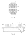
- a metal dendrite-free solar cell shown during various stages of manufacture. While a single semiconductor wafer 10 is shown yielding two of the disclosed metal dendrite-free solar cells 12, 14 ( Figs. 1C and 1D ) or solar cell assemblies ( Figs. 1C and 1E ), those skilled in the art will appreciate that the semiconductor wafer 10 may yield only one solar cell or more than two solar cells without departing from the scope of the present disclosure.
- the solar cell assemblies 12, 14 may be monolithic integrated solar cells with various electronic devices 11, such as protecting diodes, formed on the wafer wings.
- the semiconductor wafer 10 may have an upper surface 16, and may be grown on a substrate (see substrate 20 in Fig. 2 ). Portions of the upper surface 16 of the semiconductor wafer 10 may be coated with an anti-reflection coating 18. During the step of coating the upper surface 16 of the semiconductor wafer 10 with the anti-reflection coating 18, a masking material (not shown) may be applied over portions of the upper surface 16 such that only the desired portions of the upper surface 16 (i.e., the active portions) receive the anti-reflection coating 18.
- an electrical contact material 22 may be applied to portions of the upper surface 16 of the semiconductor wafer 10.
- a masking material (not shown) may be applied over portions of the upper surface 16 such that only the desired portions of the upper surface 16 receive the electrical contact material 22.
- the masking material may cover the anti-reflection coating 18 and, optionally, the areas of the semiconductor wafer 10 where isolation channels will be formed during the electrical isolation step.
- the electrical contact material 22 may be any electrically conductive material capable of being applied to the upper surface 16 of the semiconductor wafer 10.
- the electrical contact material 22 may be an electrically conductive metal or metal alloy.
- the electrical contact material 22 may be a highly electrically conductive metal or metal alloy.
- the electrical contact material 22 may be silver.
- the electrical contact material 22 may form an electrically conductive grid 24 on the upper surface 16 of the semiconductor wafer 10.
- the electrically conductive grid 24 may include grid lines 30 extending from a bus bar 32. Each grid line 30 may terminate at a grid tip 34.
- the solar cells 12, 14 may be electrically isolated from the wafer wings 26. Electrical isolation of the solar cells 12, 14 from the wafer wings 26 may be effected by forming one or more isolation channels 28 in the semiconductor wafer 10. The isolation channels 28 may extend through the semiconductor wafer 10 down to the underlying substrate 20.
- each solar cell 12, 14 may be separated from the adjacent solar cell 12, 14, and may or may not be separated from the wafer wings 26. Separation may be effected by cutting or other available means.
- metal dendrites such as silver dendrites
- a solvent e.g., deionized water.
- Metal dendrite growth may be particularly pronounced in certain solar cell fabrication processes, such as metal lift off at elevated temperatures after solar cell electrical isolation.
- Metal dendrites may obscure the passage of light to the underlying semiconductor wafer 10, thereby negatively impacting solar cell efficiency. Furthermore, metal dendrites may compromise solar cell reliability, particularly if the metal dendrites grow beyond the cap layer and contact the window layer of the solar cell structure.
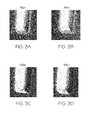
- Fig. 2 is a cross-sectional view of a portion of a solar cell wafer taken along a grid line 30.
- the grid lines 30 serve as a cathode, which has more negative charges than the electrical contact material 22 (silver) on the wafer wings 26 due to more electrical contact material coverage and wafer perimeter electrical shunting. Therefore, silver ions may transfer from the wafer wings 26, across the isolation channels 28 through the solvent (e.g., deionized water) and, ultimately, to the grid lines 30. At the grid lines 30, the silver ions may acquire electrons and may be reduced to silver, which may accumulate on the grid lines 30 as silver dendrite.
- solvent e.g., deionized water
- metal dendrite growth multiple factors may affect metal dendrite growth, including, but not limited to, the type of electrical contact material 22 used (e.g., silver), the geometry of the electrical contact material 22 on the solar cells 12, 14 and the wafer wings 26, the illumination condition, solar cell shunting resistance, and the type of solvent in which solar cell assembly is submerged. Many of these factors are dictated by the cell fabrication process being used to manufacture the solar cells 12, 14.
- the type of electrical contact material 22 used e.g., silver
- the geometry of the electrical contact material 22 on the solar cells 12, 14 and the wafer wings 26, the illumination condition, solar cell shunting resistance, and the type of solvent in which solar cell assembly is submerged are dictated by the cell fabrication process being used to manufacture the solar cells 12, 14.
- Dendrite growth rate is proportional to the electric field intensity between the solar cells 12, 14 and the wafer wings 26.
- the electrical potential difference between the solar cells 12, 14 and the wafer wings 26 may be generally constant at fixed light condition. Therefore, the shorter the distance D ( Fig. 2 ) between the grid lines 30 and the electrical contact material 22 on the wafer wings 26, the higher the electric field intensity that drives metal dendrite growth.
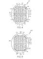
- the minimum distance D ( Fig. 2 ) between the grid lines 30 and the electrical contact material 22 on the wafer wings 26 has on metal dendrite growth four different wafer specimens were prepared with silver grid lines terminating at a tip, wherein the minimum distance D of the first specimen was 288 ⁇ m ( Fig. 3A ), the minimum distance D of the second specimen was 438 ⁇ m ( Fig. 3B ), the minimum distance D of the third specimen was 1038 ⁇ m ( Fig. 3C ) and the minimum distance D of the fourth specimen was 3438 ⁇ m ( Fig. 3D ).
- the specimens were submerged in isopropyl alcohol for 20 minutes under fluorescent room lighting conditions.
- the electrical potential difference between the cell and wafer wing was 1.83 volts.
- the grid tips were observed under 500 times magnification. The results are shown in Figs. 3A-3D .
- metal dendrite growth was reduced as the minimum distance D ( Fig. 2 ) between the grid lines 30 and the electrical contact material 22 on the wafer wings 26 increased. Significantly, little or no metal dendrite growth was observed when the distance D was about 1 mm ( Fig. 3C ), while no metal dendrite growth was observed when the distance D was about 3 mm ( Fig. 3D ).
- the orientation of the electrically conductive grid 24 may also have a significant impact on the growth rate of metal dendrites.
- the metal dendrites tend to deposit at sharp edges, specifically at the tips 34 of the grid lines 30. Without being limited to any particular theory, it is believed that the preference of dendrites to deposit on grid tips 34 is because direct current (“DC") flows more densely to the sharp edges of the grid tips 34 than the less accessible portions of the electrically conductive grid 24.
- DC direct current
- growth of metal dendrites on solar cell grid lines may be significantly reduced or eliminated by forming the solar cell assembly such that the wafer wings are substantially free of the electrical contact material.
- a solar cell assembly may include a semiconductor wafer 102, an anti-reflection coating 104 and an electrical contact material 106.
- the electrical contact material 106 may be applied in a grid pattern to form grid lines 108.
- the grid lines 108 may extend outward from a bus bar 110 and may terminate at a tip 112.
- Isolation channels may be formed in the solar cell assembly 100 to define and electrically isolate two solar cells 114, 116 from wafer wings 118.
- the wafer wings 118 may be substantially free of the electrical contact material 106 (e.g., silver) used to form the grid lines 108.
- each solar cell 114, 116 may be substantially free of metal dendrites.
- a solar cell assembly may include a semiconductor wafer 202, an anti-reflection coating 204 and an electrical contact material 206.
- the electrical contact material 206 may be applied in a grid pattern to form grid lines 208 that extend inward from a bus bar 210.
- Isolation channels may be formed in the solar cell assembly 200 to define and electrically isolate two solar cells 212, 214 from wafer wings 216.
- the wafer wings 216 may be substantially free of the electrical contact material 206 (e.g., silver) used to form the grid lines 208.
- the lack of electrical contact material 206 on the wafer wings 216 may preclude (or at least inhibit) the formation of metal dendrites on the grid lines 208.
- the grid lines 208 do not protrude toward, and open to, the wafer wings 216. Rather, the outer ends 218 of the grid lines 208 terminate at the bus bar 210 and, as such, do not present a sharp tip to the wafer wings 216, thereby further reducing the potential for dendrite formation on the grid lines 208. Therefore, when the solar cells 212, 214 are separated from the solar cell assembly 200, each solar cell 212, 214 may be substantially free of metal dendrites.
- growth of metal dendrites on solar cell grid lines may be significantly reduced or eliminated by providing a spacer zone between the grid lines and the electrical contact material on the wafer wings, wherein the spacer zone is substantially free of the electrical contact material.
- a solar cell assembly in a first implementation of the second embodiment, may include a semiconductor wafer 302, an anti-reflection coating 304 and an electrical contact material 306.
- the electrical contact material 306 may be applied in a grid pattern to form grid lines 308.
- the grid lines 308 may extend outward from a bus bar 310 and may terminate at a tip 312.
- Isolation channels may be formed in the solar cell assembly 300 to define and electrically isolate two solar cells 314, 316 from wafer wings 318.
- the wafer wings 318 may include the electrical contact material 306 (e.g., silver) used to form the grid lines 308.
- the electrical contact material 306 cannot feasibly be eliminated from the wafer wings 318.
- a test structure or other type of devices with electrical contact material 306 on the wafer wings 318 may be required or some electrical contact material 306 may be left on the wafer wings 318 to simplify the metal lift off process.
- a spacer zone 320 may be formed around the solar cells 314, 316 to space the electrical contact material 306 on the solar cells 314, 316, particularly the tips 312 of the grid lines 308, from the electrical contact material 306 on the wafer wings 318.
- the spacer zone 320 may be substantially free of the electrical contact material 306.
- the spacer zone 320 may be size and shaped to ensure a minimum distance of at least 1 millimeter between the electrical contact material 306 on the solar cells 314, 316 and the electrical contact material 306 on the wafer wings 318. In another expression, the spacer zone 320 may be size and shaped to ensure a minimum distance of at least 1.5 millimeters between the electrical contact material 306 on the solar cells 314, 316 and the electrical contact material 306 on the wafer wings 318. In another expression, the spacer zone 320 may be size and shaped to ensure a minimum distance of at least 2 millimeters between the electrical contact material 306 on the solar cells 314, 316 and the electrical contact material 306 on the wafer wings 318.
- the spacer zone 320 may be size and shaped to ensure a minimum distance of at least 2.5 millimeters between the electrical contact material 306 on the solar cells 314, 316 and the electrical contact material 306 on the wafer wings 318. In yet another expression, the spacer zone 320 may be size and shaped to ensure a minimum distance of at least 3 millimeters between the electrical contact material 306 on the solar cells 314, 316 and the electrical contact material 306 on the wafer wings 318.
- the spacer zone 320 may preclude (or at least inhibit) the formation of metal dendrites on the grid lines 308. Therefore, when the solar cells or solar cell assemblies 314, 316 are separated from the wafer, each solar cell 314, 316 may be substantially free of metal dendrites.
- a solar cell assembly may include a semiconductor wafer 402, an anti-reflection coating 404 and an electrical contact material 406.
- the electrical contact material 406 may be applied in a grid pattern to form grid lines 408 that extend inward from a bus bar 410.
- Isolation channels may be formed in the solar cell wafer 400 to define and electrically isolate two solar cells 412, 414 from wafer wings 416.
- the wafer wings 416 may include the electrical contact material 406 (e.g., silver) used to form the grid lines 408.
- a spacer zone 418 may be formed around the solar cells 412, 414 to space the electrical contact material 406 on the solar cells 412, 414 from the electrical contact material 406 on the wafer wings 416.
- the spacer zone 418 may be substantially free of the electrical contact material 406.
- the spacer zone 418 may be size and shaped to ensure a minimum distance of at least 1 millimeter between the electrical contact material 406 on the solar cells 412, 414 and the electrical contact material 406 on the wafer wings 416. In another expression, the spacer zone 418 may be size and shaped to ensure a minimum distance of at least 1.5 millimeter between the electrical contact material 406 on the solar cells 412, 414 and the electrical contact material 406 on the wafer wings 416. In another expression, the spacer zone 418 may be size and shaped to ensure a minimum distance of at least 2 millimeter between the electrical contact material 406 on the solar cells 412, 414 and the electrical contact material 406 on the wafer wings 416.
- the spacer zone 418 may be size and shaped to ensure a minimum distance of at least 2.5 millimeter between the electrical contact material 406 on the solar cells 412, 414 and the electrical contact material 406 on the wafer wings 416. In another expression, the spacer zone 418 may be size and shaped to ensure a minimum distance of at least 3 millimeter between the electrical contact material 406 on the solar cells 412, 414 and the electrical contact material 406 on the wafer wings 416.
- the spacer zone 418 may preclude (or at least inhibit) the formation of metal dendrites on the grid lines 408. Furthermore, since the grid lines 408 do not protrude toward, and open to, the wafer wings 416, but rather the outer ends 420 of the grid lines 408 terminate at the bus bar 410, no sharp tips are presented to the wafer wings 416, thereby further reducing the potential for dendrite formation on the grid lines 408. Therefore, when the solar cells or solar cell assemblies 412, 414 are separated from the wafer, each solar cell 412, 414 may be substantially free of metal dendrites.
- the disclosed solar cell may be substantially free of metal dendrites, including silver dendrites.
- the disclosed method for manufacturing solar cells may result in solar cells that are substantially free of metal dendrites, including silver dendrites.
Landscapes
- Photovoltaic Devices (AREA)
- Life Sciences & Earth Sciences (AREA)
- Sustainable Development (AREA)
- Health & Medical Sciences (AREA)
- Molecular Biology (AREA)
- Chemical & Material Sciences (AREA)
- Crystallography & Structural Chemistry (AREA)
Abstract
Description
- This application relates to solar cells, such as multijunction solar cells, and, more particularly, to solar cells that are substantially free of metal dendrites.
- Solar cells convert the sun's energy into useful electrical energy by way of the photovoltaic effect. Modem multijunction solar cells operate at efficiencies significantly higher than traditional, silicon solar cells, with the added advantage of being lightweight. Therefore, solar cells provide a reliable, lightweight and sustainable source of electrical energy suitable for a variety of terrestrial and space applications.
- A solar cell typically includes a semiconductor material having a certain energy bandgap. Photons in sunlight having energy greater than the bandgap of the semiconductor material are absorbed by the semiconductor material, thereby freeing electrons within the semiconductor material. The freed electrons diffuse through the semiconductor material and flow through a circuit as an electric current.
- Unfortunately, various components of a solar cell may interfere with the absorption of photons by the semiconductor material, thereby lowering the overall efficiency of the solar cell. Therefore, those skilled in the art continue with research and development efforts in the field of solar cells and, particularly, with research and development efforts aimed at improving solar cell efficiency.
- According to an aspect of the present invention, the disclosed metal dendrite-free solar cell assembly may include a semiconductor wafer having a solar cell portion and a wing portion, wherein the wing portion is electrically isolated from the solar cell portion, and an electrical contact material positioned on the solar cell portion, wherein the wing portion is substantially free of the electrical contact material.
- Advantageously the electrical contact material comprises an electrically conductive metal or metal alloy or a highly electrically conductive metal or metal alloy. Preferably the electrical contact material comprises silver.
- Advantageously the electrical contact material is arranged in a grid pattern.
- Preferably the grid pattern comprises a plurality of grid lines. Alternatively the grid pattern comprises a bus bar and a plurality of grid lines. Preferably the at least one grid line of said plurality of grid lines comprises a tip, wherein said tip protrudes toward said wing portion.
- Preferably the at least one grid line of said plurality of grid lines comprises an outer end, and wherein said bus bar is positioned between said outer end and said wing portion.
- Advantageously the solar cell is separated from said solar cell assembly.
- Advantageously the method for forming the solar cell may include the steps of providing a semiconductor wafer, applying an electrical contact material to the semiconductor wafer, forming an isolation channel in the semiconductor wafer to define a solar cell portion and a wing portion, wherein the wing portion is electrically isolated from the solar cell portion, and wherein the wing portion is substantially free of the electrical contact material, and separating the solar cell portion from the wing portion.
- According to a further aspect of the present invention, the disclosed metal dendrite-free solar cell assembly may include a semiconductor wafer having a solar cell portion and a wing portion, wherein the wing portion is electrically isolated from the solar cell portion, a first electrical contact material positioned on the solar cell portion and a second electrical contact material positioned on the wing portion, wherein the first electrical contact material is spaced at least 1 millimeter (or a few millimeters) from the second electrical contact material.
- Advantageously the solar cell portion is separated from said wing portion by a spacer zone, and wherein said spacer zone is substantially free of said first electrical contact material and said second electrical contact material.
- Advantageously the first electrical contact material is spaced at least 1.5 millimeters from said second electrical contact material. Alternatively the first electrical contact material is spaced at least 2 millimeters from said second electrical contact material. Alternatively, the first electrical contact material is spaced at least 2.5 millimeters from said second electrical contact material. Alternatively the first electrical contact material is spaced at least 3 millimeters from said second electrical contact material.
- Advantageously the electrical contact material comprises an electrically conductive metal or metal alloy or a highly electrically conductive metal or metal alloy. Preferably both said first electrical contact material and said second electrical contact material comprise silver.
- Advantageously the first electrical contact material is arranged in a grid pattern.
- Advantageously the grid pattern comprises a plurality of grid lines. Preferably the at least one grid line of said plurality of grid lines comprises a tip, wherein said tip protrudes toward said wing portion. Preferably the grid pattern comprises a bus bar and a plurality of grid lines. Preferably the at least one grid line of said plurality of grid lines comprises an outer end, and wherein said bus bar is positioned between said outer end and said wing portion.
- Advantageously the solar cell is separated from said solar cell assembly.
- Advantageously the method for forming a solar cell may include the steps of providing a semiconductor wafer, applying an electrical contact material to the semiconductor wafer, forming an isolation channel in the semiconductor wafer to define a solar cell portion and a wing portion, wherein the wing portion is electrically isolated from the solar cell portion, and wherein both the wing portion and the solar cell portion include the electrical contact material, forming a spacer zone between the solar cell portion and the wing portion, the spacer zone being substantially free of the electrical contact material, wherein the spacer zone spaces the electrical contact material on the wing portion a minimum of at least 1 millimeter (or a few millimeters) from the electrical contact material on the solar cell portion, and/or separating the solar cell portion from the wing portion.
- According to a further aspect of the present invention, disclosed is a method for forming a metal dendrite-free solar cell. The method may include the steps of providing a semiconductor wafer, applying an electrical contact material to the semiconductor wafer, forming an isolation channel in the semiconductor wafer to define a solar cell portion and a wing portion, wherein the wing portion is electrically isolated from the solar cell portion, and wherein both the wing portion and the solar cell portion include the electrical contact material, forming a spacer zone between the solar cell portion and the wing portion, the spacer zone being substantially free of the electrical contact material, wherein the spacer zone spaces the electrical contact material on the wing portion a minimum of at least 1 millimeter (or a few millimeters) from the electrical contact material on the solar cell portion, and/or separating the solar cell portion from the wing portion.
- According to yet another aspect of the present invention, disclosed is a method for forming a metal dendrite-free solar cell. The method may include the steps of providing a semiconductor wafer, applying an electrical contact material to the semiconductor wafer, forming an isolation channel in the semiconductor wafer to define a solar cell portion and a wing portion, wherein the wing portion is electrically isolated from the solar cell portion, and wherein the wing portion is substantially free of the electrical contact material, and separating the solar cell portion from the wing portion.
- Other aspects of the disclosed metal dendrite-free solar cell, solar cell assembly and method will become apparent from the following detailed description, the accompanying drawings and the appended claims.
-
-
Fig. 1A is a schematic top plan view of a semiconductor wafer having an anti-reflection coating applied thereto during the manufacture of the disclosed metal dendrite-free solar cell; -
Fig. 1B is a schematic top plan view of the semiconductor wafer ofFig. 1A , shown with an electrical contact material applied thereto; -
Fig. 1C is a schematic top plan view of the semiconductor wafer ofFig. 1B , shown with cell electrical isolation defining wafer wings; -
Fig. 1D is a schematic top plan view of the semiconductor wafer ofFig. 1C , shown after separation into two solar cells; -
Fig. 1E is a schematic top plan view of the semiconductor wafer ofFig. 1C , shown after separation into two solar cell assemblies which comprise solar cells and other devices on the wings; -
Fig. 2 is a schematic side elevational view, in section, of a solar cell assembly undergoing metal dendrite formation; -
Fig. 3A is a photograph of a silver grid tip that was spaced 288 µm from silver on a wafer wing during manufacture of a solar cell; -
Fig. 3B is a photograph of a silver grid tip that was spaced 438 µm from silver on a wafer wing during manufacture; -
Fig. 3C is a photograph of a silver grid tip that was spaced 1038 µm from silver on a wafer wing during manufacture of a solar cell; -
Fig. 3D is a photograph of a silver grid tip that was spaced 3438 µm from silver on a wafer wing during manufacture of a solar cell; -
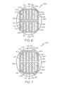
Fig. 4 is a top plan view of a first implementation of a first embodiment of the disclosed metal dendrite-free solar cell; -
Fig. 5 is a top plan view of a second implementation of the first embodiment of the disclosed metal dendrite-free solar cell; -
Fig. 6 is a top plan view of a first implementation of a second embodiment of the disclosed metal dendrite-free solar cell; and -
Fig. 7 is a top plan view of a second implementation of the second embodiment of the disclosed metal dendrite-free solar cell. - Silver is often used in the manufacture of multiple junction solar cells as an electrical contact metal due to its high conductivity. Under fluorescent light illumination, which is used in most solar cell manufacturing environments, for a typical triple junction solar cell, the metal grid contact (front side) serves as the cathode of the cell, which has more negative charges than the silver metal contact on the wings due to more metal coverage and wafer perimeter electrical shunting. The silver ions from wings are transferred through aqueous medium to cell grids and reduced to silver dendrite by acquiring electrons. The silver dendrite introduces obscurity to sun light and reduces solar cell efficiency and compromises solar cell reliability. Therefore, disclosed are solar cell wafer front metal contact designs that reduce or eliminate silver dendrite growth on the metal grid.
- Referring to
Figs. 1A-1E , disclosed is a metal dendrite-free solar cell shown during various stages of manufacture. While asingle semiconductor wafer 10 is shown yielding two of the disclosed metal dendrite-freesolar cells 12, 14 (Figs. 1C and 1D ) or solar cell assemblies (Figs. 1C and1E ), those skilled in the art will appreciate that thesemiconductor wafer 10 may yield only one solar cell or more than two solar cells without departing from the scope of the present disclosure. - As shown in
Fig. 1E , thesolar cell assemblies electronic devices 11, such as protecting diodes, formed on the wafer wings. - As shown in
Fig. 1A , thesemiconductor wafer 10 may have anupper surface 16, and may be grown on a substrate (seesubstrate 20 inFig. 2 ). Portions of theupper surface 16 of thesemiconductor wafer 10 may be coated with ananti-reflection coating 18. During the step of coating theupper surface 16 of thesemiconductor wafer 10 with theanti-reflection coating 18, a masking material (not shown) may be applied over portions of theupper surface 16 such that only the desired portions of the upper surface 16 (i.e., the active portions) receive theanti-reflection coating 18. - As shown in
Fig. 1B , anelectrical contact material 22 may be applied to portions of theupper surface 16 of thesemiconductor wafer 10. During the step of applying theelectrical contact material 22 to theupper surface 16 of thesemiconductor wafer 10, a masking material (not shown) may be applied over portions of theupper surface 16 such that only the desired portions of theupper surface 16 receive theelectrical contact material 22. For example, the masking material may cover theanti-reflection coating 18 and, optionally, the areas of thesemiconductor wafer 10 where isolation channels will be formed during the electrical isolation step. - The
electrical contact material 22 may be any electrically conductive material capable of being applied to theupper surface 16 of thesemiconductor wafer 10. In one general expression, theelectrical contact material 22 may be an electrically conductive metal or metal alloy. In another general expression, theelectrical contact material 22 may be a highly electrically conductive metal or metal alloy. In one particular expression, theelectrical contact material 22 may be silver. - Thus, the
electrical contact material 22 may form an electricallyconductive grid 24 on theupper surface 16 of thesemiconductor wafer 10. The electricallyconductive grid 24 may includegrid lines 30 extending from abus bar 32. Eachgrid line 30 may terminate at agrid tip 34. - As shown in
Fig. 1C , thesolar cells wafer wings 26. Electrical isolation of thesolar cells wafer wings 26 may be effected by forming one ormore isolation channels 28 in thesemiconductor wafer 10. Theisolation channels 28 may extend through thesemiconductor wafer 10 down to theunderlying substrate 20. - Finally, as shown in
Figs. 1D and1E , with thesolar cells wafer wings 26, thesolar cells solar cell solar cell wafer wings 26. Separation may be effected by cutting or other available means. - It has been discovered that metal dendrites, such as silver dendrites, may form on the
grid lines 30 of the electricallyconductive grid 24, particularly on thegrid tips 34 of the grid lines 30, after thesolar cells wafer wings 26, as shown inFig. 1C , and submerged in a solvent (e.g., deionized water). Metal dendrite growth may be particularly pronounced in certain solar cell fabrication processes, such as metal lift off at elevated temperatures after solar cell electrical isolation. - Metal dendrites may obscure the passage of light to the
underlying semiconductor wafer 10, thereby negatively impacting solar cell efficiency. Furthermore, metal dendrites may compromise solar cell reliability, particularly if the metal dendrites grow beyond the cap layer and contact the window layer of the solar cell structure. - The mechanism of silver dendrite growth is shown in
Fig. 2 , which is a cross-sectional view of a portion of a solar cell wafer taken along agrid line 30. Under certain lighting conditions, such as thefluorescent light 36 typically found in the solar cell manufacturing environment, the grid lines 30 (silver) serve as a cathode, which has more negative charges than the electrical contact material 22 (silver) on thewafer wings 26 due to more electrical contact material coverage and wafer perimeter electrical shunting. Therefore, silver ions may transfer from thewafer wings 26, across theisolation channels 28 through the solvent (e.g., deionized water) and, ultimately, to the grid lines 30. At the grid lines 30, the silver ions may acquire electrons and may be reduced to silver, which may accumulate on thegrid lines 30 as silver dendrite. - Multiple factors may affect metal dendrite growth, including, but not limited to, the type of
electrical contact material 22 used (e.g., silver), the geometry of theelectrical contact material 22 on thesolar cells wafer wings 26, the illumination condition, solar cell shunting resistance, and the type of solvent in which solar cell assembly is submerged. Many of these factors are dictated by the cell fabrication process being used to manufacture thesolar cells - Dendrite growth rate is proportional to the electric field intensity between the
solar cells wafer wings 26. The electrical potential difference between thesolar cells wafer wings 26 may be generally constant at fixed light condition. Therefore, the shorter the distance D (Fig. 2 ) between thegrid lines 30 and theelectrical contact material 22 on thewafer wings 26, the higher the electric field intensity that drives metal dendrite growth. - To show the effect that the minimum distance D (
Fig. 2 ) between thegrid lines 30 and theelectrical contact material 22 on thewafer wings 26 has on metal dendrite growth, four different wafer specimens were prepared with silver grid lines terminating at a tip, wherein the minimum distance D of the first specimen was 288 µm (Fig. 3A ), the minimum distance D of the second specimen was 438 µm (Fig. 3B ), the minimum distance D of the third specimen was 1038 µm (Fig. 3C ) and the minimum distance D of the fourth specimen was 3438 µm (Fig. 3D ). The specimens were submerged in isopropyl alcohol for 20 minutes under fluorescent room lighting conditions. The electrical potential difference between the cell and wafer wing was 1.83 volts. After the twenty minute bath, the grid tips were observed under 500 times magnification. The results are shown inFigs. 3A-3D . - As can be seen in
Figs. 3A-3D , metal dendrite growth was reduced as the minimum distance D (Fig. 2 ) between thegrid lines 30 and theelectrical contact material 22 on thewafer wings 26 increased. Significantly, little or no metal dendrite growth was observed when the distance D was about 1 mm (Fig. 3C ), while no metal dendrite growth was observed when the distance D was about 3 mm (Fig. 3D ). - In addition to the distance D between the
grid lines 30 and theelectrical contact material 22 on thewafer wings 26, the orientation of the electricallyconductive grid 24 may also have a significant impact on the growth rate of metal dendrites. The metal dendrites tend to deposit at sharp edges, specifically at thetips 34 of the grid lines 30. Without being limited to any particular theory, it is believed that the preference of dendrites to deposit ongrid tips 34 is because direct current ("DC") flows more densely to the sharp edges of thegrid tips 34 than the less accessible portions of the electricallyconductive grid 24. - In a first embodiment, growth of metal dendrites on solar cell grid lines may be significantly reduced or eliminated by forming the solar cell assembly such that the wafer wings are substantially free of the electrical contact material.
- Referring to
Fig. 4 , in a first implementation of the first embodiment, a solar cell assembly, generally designated 100, may include asemiconductor wafer 102, ananti-reflection coating 104 and anelectrical contact material 106. Theelectrical contact material 106 may be applied in a grid pattern to form grid lines 108. The grid lines 108 may extend outward from abus bar 110 and may terminate at atip 112. - Isolation channels (see
channel 28 inFig. 2 ) may be formed in thesolar cell assembly 100 to define and electrically isolate twosolar cells wafer wings 118. Thewafer wings 118 may be substantially free of the electrical contact material 106 (e.g., silver) used to form the grid lines 108. - Thus, despite the
tips 112 of thegrid lines 108 protruding toward thewafer wings 118, the lack ofelectrical contact material 106 on thewafer wings 118 may preclude (or at least inhibit) the formation of metal dendrites on the grid lines 108. Therefore, when thesolar cells Fig. 1D , eachsolar cell - Referring to
Fig. 5 , in a second implementation of the first embodiment, a solar cell assembly, generally designated 200, may include asemiconductor wafer 202, an anti-reflection coating 204 and anelectrical contact material 206. Theelectrical contact material 206 may be applied in a grid pattern to formgrid lines 208 that extend inward from abus bar 210. - Isolation channels may be formed in the
solar cell assembly 200 to define and electrically isolate twosolar cells wafer wings 216. Thewafer wings 216 may be substantially free of the electrical contact material 206 (e.g., silver) used to form the grid lines 208. - Thus, the lack of
electrical contact material 206 on thewafer wings 216 may preclude (or at least inhibit) the formation of metal dendrites on the grid lines 208. Furthermore, in the second implementation, thegrid lines 208 do not protrude toward, and open to, thewafer wings 216. Rather, the outer ends 218 of thegrid lines 208 terminate at thebus bar 210 and, as such, do not present a sharp tip to thewafer wings 216, thereby further reducing the potential for dendrite formation on the grid lines 208. Therefore, when thesolar cells solar cell assembly 200, eachsolar cell - In a second embodiment, growth of metal dendrites on solar cell grid lines may be significantly reduced or eliminated by providing a spacer zone between the grid lines and the electrical contact material on the wafer wings, wherein the spacer zone is substantially free of the electrical contact material.
- Referring to
Fig. 6 , in a first implementation of the second embodiment, a solar cell assembly, generally designated 300, may include a semiconductor wafer 302, ananti-reflection coating 304 and anelectrical contact material 306. Theelectrical contact material 306 may be applied in a grid pattern to form grid lines 308. The grid lines 308 may extend outward from abus bar 310 and may terminate at atip 312. - Isolation channels may be formed in the
solar cell assembly 300 to define and electrically isolate twosolar cells wafer wings 318. Thewafer wings 318 may include the electrical contact material 306 (e.g., silver) used to form the grid lines 308. - At this point, those skilled in the art will appreciate that in certain situations the
electrical contact material 306 cannot feasibly be eliminated from thewafer wings 318. For example, a test structure or other type of devices withelectrical contact material 306 on thewafer wings 318 may be required or someelectrical contact material 306 may be left on thewafer wings 318 to simplify the metal lift off process. - Therefore, a
spacer zone 320 may be formed around thesolar cells electrical contact material 306 on thesolar cells tips 312 of thegrid lines 308, from theelectrical contact material 306 on thewafer wings 318. Thespacer zone 320 may be substantially free of theelectrical contact material 306. - In one expression, the
spacer zone 320 may be size and shaped to ensure a minimum distance of at least 1 millimeter between theelectrical contact material 306 on thesolar cells electrical contact material 306 on thewafer wings 318. In another expression, thespacer zone 320 may be size and shaped to ensure a minimum distance of at least 1.5 millimeters between theelectrical contact material 306 on thesolar cells electrical contact material 306 on thewafer wings 318. In another expression, thespacer zone 320 may be size and shaped to ensure a minimum distance of at least 2 millimeters between theelectrical contact material 306 on thesolar cells electrical contact material 306 on thewafer wings 318. In another expression, thespacer zone 320 may be size and shaped to ensure a minimum distance of at least 2.5 millimeters between theelectrical contact material 306 on thesolar cells electrical contact material 306 on thewafer wings 318. In yet another expression, thespacer zone 320 may be size and shaped to ensure a minimum distance of at least 3 millimeters between theelectrical contact material 306 on thesolar cells electrical contact material 306 on thewafer wings 318. - Thus, despite the
tips 312 of thegrid lines 308 protruding toward, and opening to, thewafer wings 318, thespacer zone 320 may preclude (or at least inhibit) the formation of metal dendrites on the grid lines 308. Therefore, when the solar cells orsolar cell assemblies solar cell - Referring to
Fig. 7 , in a second implementation of the second embodiment, a solar cell assembly, generally designated 400, may include a semiconductor wafer 402, ananti-reflection coating 404 and anelectrical contact material 406. Theelectrical contact material 406 may be applied in a grid pattern to formgrid lines 408 that extend inward from abus bar 410. - Isolation channels may be formed in the
solar cell wafer 400 to define and electrically isolate twosolar cells wafer wings 416. Thewafer wings 416 may include the electrical contact material 406 (e.g., silver) used to form the grid lines 408. - A
spacer zone 418 may be formed around thesolar cells electrical contact material 406 on thesolar cells electrical contact material 406 on thewafer wings 416. Thespacer zone 418 may be substantially free of theelectrical contact material 406. - In one expression, the
spacer zone 418 may be size and shaped to ensure a minimum distance of at least 1 millimeter between theelectrical contact material 406 on thesolar cells electrical contact material 406 on thewafer wings 416. In another expression, thespacer zone 418 may be size and shaped to ensure a minimum distance of at least 1.5 millimeter between theelectrical contact material 406 on thesolar cells electrical contact material 406 on thewafer wings 416. In another expression, thespacer zone 418 may be size and shaped to ensure a minimum distance of at least 2 millimeter between theelectrical contact material 406 on thesolar cells electrical contact material 406 on thewafer wings 416. In another expression, thespacer zone 418 may be size and shaped to ensure a minimum distance of at least 2.5 millimeter between theelectrical contact material 406 on thesolar cells electrical contact material 406 on thewafer wings 416. In another expression, thespacer zone 418 may be size and shaped to ensure a minimum distance of at least 3 millimeter between theelectrical contact material 406 on thesolar cells electrical contact material 406 on thewafer wings 416. - Thus, the
spacer zone 418 may preclude (or at least inhibit) the formation of metal dendrites on the grid lines 408. Furthermore, since thegrid lines 408 do not protrude toward, and open to, thewafer wings 416, but rather the outer ends 420 of thegrid lines 408 terminate at thebus bar 410, no sharp tips are presented to thewafer wings 416, thereby further reducing the potential for dendrite formation on the grid lines 408. Therefore, when the solar cells orsolar cell assemblies solar cell - Accordingly, the disclosed solar cell may be substantially free of metal dendrites, including silver dendrites. Furthermore, the disclosed method for manufacturing solar cells may result in solar cells that are substantially free of metal dendrites, including silver dendrites.
- Although various aspects of the disclosed metal dendrite-free solar cell have been shown and described, modifications may occur to those skilled in the art upon reading the specification. The present application includes such modifications and is limited only by the scope of the claims.
- Further, the current invention comprises embodiments according to the following clauses:
- Clause 1. A solar cell assembly comprising:
- a semiconductor wafer comprising a solar cell portion and a wing portion, wherein said wing portion is electrically isolated from said solar cell portion; and
- an electrical contact material positioned on said solar cell portion,
- wherein said wing portion is substantially free of said electrical contact material.
- Clause 2. The solar cell assembly of clause 1 wherein said electrical contact material comprises silver.
- Clause 3. The solar cell assembly of clause 1 or 2 wherein said electrical contact material is arranged in a grid pattern.
- Clause 4. The solar cell assembly of clause 3 wherein said grid pattern comprises a plurality of grid lines.
- Clause 5. The solar cell assembly of clause 4 wherein at least one grid line of said plurality of grid lines comprises a tip, wherein said tip protrudes toward said wing portion.
- Clause 6. The solar cell assembly of clause 3 wherein said grid pattern comprises a bus bar and a plurality of grid lines.
- Clause 7. The solar cell assembly of clause 6 wherein at least one grid line of said plurality of grid lines comprises an outer end, and wherein said bus bar is positioned between said outer end and said wing portion.
- Clause 8. A solar cell separated from said solar cell assembly of any of clauses 1 to 7.
- Clause 9. A solar cell assembly comprising:
- a semiconductor wafer comprising a solar cell portion and a wing portion, wherein said wing portion is electrically isolated from said solar cell portion;
- a first electrical contact material positioned on said solar cell portion; and
- a second electrical contact material positioned on said wing portion,
- wherein said first electrical contact material is spaced at least 1 millimeter from said second electrical contact material.
-
Clause 10. The solar cell assembly of clause 9 wherein said solar cell portion is separated from said wing portion by a spacer zone, and wherein said spacer zone is substantially free of said first electrical contact material and said second electrical contact material. -
Clause 11. The solar cell assembly ofclause 9 or 10 wherein said first electrical contact material is spaced at least 1.5 millimeters from said second electrical contact material. -
Clause 12. The solar cell assembly ofclause 9 or 10 wherein said first electrical contact material is spaced at least 2 millimeters from said second electrical contact material. - Clause 13. The solar cell assembly of
clause 9 or 10 wherein said first electrical contact material is spaced at least 2.5 millimeters from said second electrical contact material. -
Clause 14. The solar cell assembly ofclause 9 or 10 wherein said first electrical contact material is spaced at least 3 millimeters from said second electrical contact material. - Clause 15. The solar cell assembly of any of clauses 9 to 14 wherein both said first electrical contact material and said second electrical contact material comprise silver.
-
Clause 16. The solar cell assembly of any of clauses 9 to 15 wherein said first electrical contact material is arranged in a grid pattern. - Clause 17. The solar cell assembly of
clause 16 wherein said grid pattern comprises a plurality of grid lines. -
Clause 18. The solar cell assembly of clause 17 wherein at least one grid line of said plurality of grid lines comprises a tip, wherein said tip protrudes toward said wing portion. - Clause 19. The solar cell assembly of
clause 16 wherein said grid pattern comprises a bus bar and a plurality of grid lines. -
Clause 20. The solar cell assembly of clause 19 wherein at least one grid line of said plurality of grid lines comprises an outer end, and wherein said bus bar is positioned between said outer end and said wing portion.
Claims (10)
- A solar cell assembly comprising:a semiconductor wafer (10, 102) comprising a solar cell portion (12, 14, 114, 116) and a wing (26, 118) portion, wherein said wing (26, 118) portion is electrically isolated from said solar cell portion (12, 14, 114, 116); andan electrical contact material (22, 106) positioned on said solar cell portion (12, 14, 114, 116),wherein said wing (26,118) portion is substantially free of said electrical contact material (22, 106).
- The solar cell assembly of Claim 1 wherein said electrical contact material (22, 106) comprisesan electrically conductive metal or metal alloy or a highly conductive metal or metal alloy.
- The solar cell assembly of Claim 1 or 2, wherein said electrical contact material (22, 106) comprises silver.
- The solar cell assembly of Claim 1 wherein said electrical contact material (22, 106) is arranged in a grid (24) pattern.
- The solar cell assembly of Claim 4 wherein said grid (24) pattern comprises a plurality of grid lines (30, 108).
- The solar cell assembly of Claim 5 wherein at least one grid line (30) of said plurality of grid lines (30, 108) comprises a tip (34, 112), wherein said tip (34, 112) protrudes toward said wing (26, 118) portion.
- The solar cell assembly of Claim 4 wherein said grid (30) pattern comprises a bus bar (32, 110) and a plurality of grid lines (30, 108).
- The solar cell assembly of Claim 7 wherein at least one grid line (30, 108) of said plurality of grid lines (30) comprises an outer end, and wherein said bus bar (32, 110) is positioned between said outer end and said wing (26, 118) portion.
- A solar cell (12, 14, 114, 116) separated from said solar cell assembly of any of Claims 1-8.
- A method for forming the solar cell (12, 14, 114, 116) of Claim 9 comprising the steps of:providing a semiconductor wafer (10, 102);applying an electrical contact material (22, 106) to the semiconductor wafer (10, 102);forming an isolation channel (28) in the semiconductor wafer to define a solar cell (12, 14, 114, 116) portion and a wing (26, 118) portion, wherein the wing (26, 118) portion is electrically isolated from the solar cell (12, 14, 114, 116) portion, and wherein the wing (26, 118) portion is substantially free of the electrical contact material (22, 106); and separating the solar cell (12, 14, 114, 116) portion from the wing (26, 118) portion.
Applications Claiming Priority (1)
| Application Number | Priority Date | Filing Date | Title |
|---|---|---|---|
| US13/423,231 US20130240009A1 (en) | 2012-03-18 | 2012-03-18 | Metal Dendrite-free Solar Cell |
Publications (2)
| Publication Number | Publication Date |
|---|---|
| EP2642526A2 true EP2642526A2 (en) | 2013-09-25 |
| EP2642526A3 EP2642526A3 (en) | 2016-08-17 |
Family
ID=47884177
Family Applications (1)
| Application Number | Title | Priority Date | Filing Date |
|---|---|---|---|
| EP13159060.6A Ceased EP2642526A3 (en) | 2012-03-18 | 2013-03-13 | Metal dentrite-free solar cell |
Country Status (4)
| Country | Link |
|---|---|
| US (3) | US20130240009A1 (en) |
| EP (1) | EP2642526A3 (en) |
| CN (1) | CN103325795A (en) |
| TW (2) | TWI685121B (en) |
Families Citing this family (4)
| Publication number | Priority date | Publication date | Assignee | Title |
|---|---|---|---|---|
| US20130240009A1 (en) * | 2012-03-18 | 2013-09-19 | The Boeing Company | Metal Dendrite-free Solar Cell |
| CN106100570B (en) * | 2016-06-12 | 2018-01-16 | 上海空间电源研究所 | A kind of semi-rigid solar cell circuit module and its mount method |
| US11978815B2 (en) | 2018-12-27 | 2024-05-07 | Solarpaint Ltd. | Flexible photovoltaic cell, and methods and systems of producing it |
| US11081606B2 (en) * | 2018-12-27 | 2021-08-03 | Solarpaint Ltd. | Flexible and rollable photovoltaic cell having enhanced properties of mechanical impact absorption |
Family Cites Families (24)
| Publication number | Priority date | Publication date | Assignee | Title |
|---|---|---|---|---|
| US4105471A (en) * | 1977-06-08 | 1978-08-08 | Arco Solar, Inc. | Solar cell with improved printed contact and method of making the same |
| JP3156973B2 (en) * | 1991-10-18 | 2001-04-16 | キヤノン株式会社 | Solar cell |
| US5340409A (en) * | 1992-04-23 | 1994-08-23 | Canon Kabushiki Kaisha | Photovoltaic element and method for forming the same |
| US5428249A (en) * | 1992-07-15 | 1995-06-27 | Canon Kabushiki Kaisha | Photovoltaic device with improved collector electrode |
| US5986204A (en) * | 1996-03-21 | 1999-11-16 | Canon Kabushiki Kaisha | Photovoltaic cell |
| US6488820B1 (en) * | 1999-08-23 | 2002-12-03 | Applied Materials, Inc. | Method and apparatus for reducing migration of conductive material on a component |
| US6825135B2 (en) * | 2002-06-06 | 2004-11-30 | Micron Technology, Inc. | Elimination of dendrite formation during metal/chalcogenide glass deposition |
| JP2005142268A (en) * | 2003-11-05 | 2005-06-02 | Canon Inc | Photovoltaic element and manufacturing method thereof |
| DE102004023856B4 (en) * | 2004-05-12 | 2006-07-13 | Rwe Space Solar Power Gmbh | Solar cell with integrated protection diode and additionally arranged on this tunnel diode |
| JP5171001B2 (en) * | 2005-09-30 | 2013-03-27 | 三洋電機株式会社 | Method for manufacturing solar cell module, solar cell and solar cell module |
| US7687707B2 (en) * | 2005-11-16 | 2010-03-30 | Emcore Solar Power, Inc. | Via structures in solar cells with bypass diode |
| JP4909032B2 (en) * | 2006-11-30 | 2012-04-04 | 三洋電機株式会社 | Solar cell module |
| US7851696B2 (en) * | 2006-12-08 | 2010-12-14 | Q-Cells Se | Solar cell |
| JP5142565B2 (en) * | 2007-03-20 | 2013-02-13 | 三洋電機株式会社 | Manufacturing method of solar cell |
| US20100012175A1 (en) * | 2008-07-16 | 2010-01-21 | Emcore Solar Power, Inc. | Ohmic n-contact formed at low temperature in inverted metamorphic multijunction solar cells |
| US20090283145A1 (en) * | 2008-05-13 | 2009-11-19 | Kim Yun-Gi | Semiconductor Solar Cells Having Front Surface Electrodes |
| US8263853B2 (en) * | 2008-08-07 | 2012-09-11 | Emcore Solar Power, Inc. | Wafer level interconnection of inverted metamorphic multijunction solar cells |
| US20100089447A1 (en) * | 2008-10-09 | 2010-04-15 | Solopower, Inc. | Conductive grids for solar cells |
| EP2214213A2 (en) * | 2009-01-29 | 2010-08-04 | SCHOTT Solar AG | Photovoltaic module |
| US7960201B2 (en) * | 2009-01-29 | 2011-06-14 | Emcore Solar Power, Inc. | String interconnection and fabrication of inverted metamorphic multijunction solar cells |
| US8337942B2 (en) * | 2009-08-28 | 2012-12-25 | Minsek David W | Light induced plating of metals on silicon photovoltaic cells |
| KR20110135203A (en) * | 2010-06-10 | 2011-12-16 | 삼성전자주식회사 | Solar cell module and manufacturing method thereof |
| JPWO2012086703A1 (en) * | 2010-12-22 | 2014-05-22 | 京セラ株式会社 | Photoelectric conversion device |
| US20130240009A1 (en) * | 2012-03-18 | 2013-09-19 | The Boeing Company | Metal Dendrite-free Solar Cell |
-
2012
- 2012-03-18 US US13/423,231 patent/US20130240009A1/en not_active Abandoned
-
2013
- 2013-02-22 CN CN2013100571376A patent/CN103325795A/en active Pending
- 2013-03-13 EP EP13159060.6A patent/EP2642526A3/en not_active Ceased
- 2013-03-13 TW TW102108757A patent/TWI685121B/en not_active IP Right Cessation
- 2013-03-13 TW TW106121997A patent/TWI685122B/en not_active IP Right Cessation
-
2017
- 2017-04-17 US US15/488,618 patent/US10224440B2/en not_active Expired - Fee Related
-
2019
- 2019-01-16 US US16/249,015 patent/US11139407B2/en not_active Expired - Fee Related
Non-Patent Citations (1)
| Title |
|---|
| None * |
Also Published As
| Publication number | Publication date |
|---|---|
| US20190148572A1 (en) | 2019-05-16 |
| US20170222070A1 (en) | 2017-08-03 |
| TWI685121B (en) | 2020-02-11 |
| US20130240009A1 (en) | 2013-09-19 |
| US10224440B2 (en) | 2019-03-05 |
| TW201349528A (en) | 2013-12-01 |
| TW201737505A (en) | 2017-10-16 |
| US11139407B2 (en) | 2021-10-05 |
| CN103325795A (en) | 2013-09-25 |
| TWI685122B (en) | 2020-02-11 |
| EP2642526A3 (en) | 2016-08-17 |
Similar Documents
| Publication | Publication Date | Title |
|---|---|---|
| US11139407B2 (en) | Metal dendrite-free solar cell | |
| US8293568B2 (en) | Crystalline silicon PV cell with selective emitter produced with low temperature precision etch back and passivation process | |
| TWI565092B (en) | Porous semiconductor photovoltaic cells designed with contact terminals/electrolytic etching modules and related production lines | |
| WO2010150947A1 (en) | Solar cell and fabrication method thereof | |
| US20170278998A1 (en) | Manufacturing method for solar cell and solar cell | |
| US20120270356A1 (en) | Method for manufacturing a solar cell | |
| JP2013537364A (en) | Photovoltaic power generation apparatus and manufacturing method thereof | |
| TW201405854A (en) | Solar cell unit cell manufacturing method | |
| TW201025622A (en) | Electrode for solar cell and fabricating method thereof | |
| US20140026936A1 (en) | Photovoltaic solar cell and a method for the production of same | |
| US20150214394A1 (en) | Opto-electrical conversion structure | |
| US4401840A (en) | Semicrystalline solar cell | |
| EP0721666A1 (en) | Process for metallising solar cells made of crystalline silicon | |
| WO2013094556A1 (en) | Solar cell with wiring sheet, solar cell module, and solar cell manufacturing method | |
| KR101193021B1 (en) | Solar cell having dot type electrode and manufacturing method of the same | |
| CN106653895B (en) | Local doped crystalline silicon solar cell and preparation method thereof | |
| Oh et al. | Investigation of selective emitter in single step diffusion process for plated Ni/Cu metallization crystalline silicon solar cells | |
| EP2528106A1 (en) | Photovoltaic power generation device and manufacturing method thereof | |
| TW201431108A (en) | A process of manufacturing an interdigitated back-contact solar cell | |
| JP2005260158A (en) | Solar cell module | |
| KR100322708B1 (en) | Method for fabricating self-voltage applying solar cell | |
| KR101382047B1 (en) | Method for fabricating selective emitter structure of solar cell | |
| KR101189378B1 (en) | Solar cell module and method of fabricating the same | |
| Malevskaya et al. | Effect of bus-bar material and configuration on the efficiency of GaInP/GaAs/Ge solar cells | |
| KR20240092798A (en) | Method For Manufacturing Solar Cell To Produce Renewable Energy |
Legal Events
| Date | Code | Title | Description |
|---|---|---|---|
| PUAI | Public reference made under article 153(3) epc to a published international application that has entered the european phase |
Free format text: ORIGINAL CODE: 0009012 |
|
| AK | Designated contracting states |
Kind code of ref document: A2 Designated state(s): AL AT BE BG CH CY CZ DE DK EE ES FI FR GB GR HR HU IE IS IT LI LT LU LV MC MK MT NL NO PL PT RO RS SE SI SK SM TR |
|
| AX | Request for extension of the european patent |
Extension state: BA ME |
|
| PUAL | Search report despatched |
Free format text: ORIGINAL CODE: 0009013 |
|
| AK | Designated contracting states |
Kind code of ref document: A3 Designated state(s): AL AT BE BG CH CY CZ DE DK EE ES FI FR GB GR HR HU IE IS IT LI LT LU LV MC MK MT NL NO PL PT RO RS SE SI SK SM TR |
|
| AX | Request for extension of the european patent |
Extension state: BA ME |
|
| RIC1 | Information provided on ipc code assigned before grant |
Ipc: H01L 31/18 20060101ALI20160712BHEP Ipc: H01L 31/0224 20060101AFI20160712BHEP |
|
| STAA | Information on the status of an ep patent application or granted ep patent |
Free format text: STATUS: REQUEST FOR EXAMINATION WAS MADE |
|
| 17P | Request for examination filed |
Effective date: 20170125 |
|
| RBV | Designated contracting states (corrected) |
Designated state(s): AL AT BE BG CH CY CZ DE DK EE ES FI FR GB GR HR HU IE IS IT LI LT LU LV MC MK MT NL NO PL PT RO RS SE SI SK SM TR |
|
| STAA | Information on the status of an ep patent application or granted ep patent |
Free format text: STATUS: EXAMINATION IS IN PROGRESS |
|
| 17Q | First examination report despatched |
Effective date: 20190503 |
|
| STAA | Information on the status of an ep patent application or granted ep patent |
Free format text: STATUS: THE APPLICATION HAS BEEN REFUSED |
|
| 18R | Application refused |
Effective date: 20221113 |
|
| RAP3 | Party data changed (applicant data changed or rights of an application transferred) |
Owner name: THE BOEING COMPANY |