EP2642372A1 - Touch-controlled electronic device and method for reducing wireless signal interference to touch sensing function - Google Patents
Touch-controlled electronic device and method for reducing wireless signal interference to touch sensing function Download PDFInfo
- Publication number
- EP2642372A1 EP2642372A1 EP12006045.4A EP12006045A EP2642372A1 EP 2642372 A1 EP2642372 A1 EP 2642372A1 EP 12006045 A EP12006045 A EP 12006045A EP 2642372 A1 EP2642372 A1 EP 2642372A1
- Authority
- EP
- European Patent Office
- Prior art keywords
- touch
- wireless communication
- synchronous signal
- communication module
- module
- Prior art date
- Legal status (The legal status is an assumption and is not a legal conclusion. Google has not performed a legal analysis and makes no representation as to the accuracy of the status listed.)
- Granted
Links
Images

Classifications
-
- G—PHYSICS
- G06—COMPUTING OR CALCULATING; COUNTING
- G06F—ELECTRIC DIGITAL DATA PROCESSING
- G06F3/00—Input arrangements for transferring data to be processed into a form capable of being handled by the computer; Output arrangements for transferring data from processing unit to output unit, e.g. interface arrangements
- G06F3/01—Input arrangements or combined input and output arrangements for interaction between user and computer
- G06F3/03—Arrangements for converting the position or the displacement of a member into a coded form
- G06F3/041—Digitisers, e.g. for touch screens or touch pads, characterised by the transducing means
- G06F3/0416—Control or interface arrangements specially adapted for digitisers
- G06F3/0418—Control or interface arrangements specially adapted for digitisers for error correction or compensation, e.g. based on parallax, calibration or alignment
-
- G—PHYSICS
- G06—COMPUTING OR CALCULATING; COUNTING
- G06F—ELECTRIC DIGITAL DATA PROCESSING
- G06F2203/00—Indexing scheme relating to G06F3/00 - G06F3/048
- G06F2203/041—Indexing scheme relating to G06F3/041 - G06F3/045
- G06F2203/04107—Shielding in digitiser, i.e. guard or shielding arrangements, mostly for capacitive touchscreens, e.g. driven shields, driven grounds
Definitions
- the present invention relates to a touch-controlled electronic device with a wireless communication function, and in particular relates to an electronic device capable of reducing wireless signal interference to touch sensing function.
- the touch sensing function is extremely susceptible to wireless wave interference.
- the wireless communication module is a near field communication module (NFC module, built in an electronic device for implementing an E-Ticket, an E-Card, a Radio-Frequency identification device and so on)
- NFC module near field communication module
- the Radio-Frequency (RF) waveform emitted from the antenna may considerably affect the touch sensing function of the projective capacitive touch panel when the wireless communication module enters a card reader mode or a peer-to-peer transmission mode.
- the technological field is in dire need of developing solutions to cope with wireless signal interference to the touch sensing function.
- a touch-controlled electronic device with a wireless communication function and a method of reducing wireless signal interference to a touch sensing function are disclosed.
- the disclosed touch-controlled electronic device comprises a wireless communication module, a touch sensing module and a synchronous signal interface.
- the wireless communication module has an antenna for receiving or transmitting a wireless signal.
- the touch sensing module is used for sensing a touch of an object.
- the synchronous signal interface is coupled between the touch sensing module and the wireless communication module for transmitting a synchronous signal.
- the touch sensing module stops sensing the touch according to the synchronous signal.
- the touch sensing module is used for sensing a touch of an objective
- the wireless communication module has an antenna for receiving or transmitting a wireless signal.
- the synchronous signal interface is coupled between the touch sensing module and the wireless communication module for transmitting a synchronous signal.
- the wireless communication module stops receiving or stops transmitting the wireless signal according to the synchronous signal.
- the disclosed method for reducing wireless signal interference to the touch sensing function is applied in a touch-controlled electronic device.
- the touch-controlled electronic device has a wireless communication module and a touch sensing module.
- the disclosed method comprises the steps as follows: receiving or transmitting a wireless signal by the wireless communication module; transmitting a synchronous signal to the wireless communication module when the touch sensing module senses a touch of an object; and according to the synchronous signal, stopping receiving or transmitting the wireless signal by the wireless communication module.
- the disclosed method for reducing wireless signal interference to the touch sensing function comprises the steps as follows: sensing a touch of an object by the touch sensing module; transmitting a synchronous signal to the touch sensing module when the wireless communication module transmits or receives a wireless signal; and according to the synchronous signal, stopping sensing the touch by the touch sensing module.
- Fig. 1 is a block diagram depicting an electronic device 100 in accordance with an exemplary embodiment of the invention
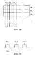
- Fig. 2A and Fig. 2B illustrate the operations of a projective capacitive touch panel 110
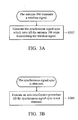
- Fig. 3A and Fig. 3B show a flowchart depicting an example in which the synchronous signal sync is provided from the wireless communication module 102;
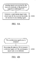
- Fig. 4A and Fig. 4B show a flowchart depicting an example in which the synchronous signal sync is provided from the touch sensing module 104.
- Fig. 1 is a block diagram depicting an electronic device 100 in accordance with an exemplary embodiment of the invention.
- the electronic device 100 comprises a wireless communication module 102, a touch sensing module 104 and at least one synchronous signal interface 105 electrically coupled between the wireless communication module 102 and the touch sensing module 104.
- the wireless communication module 102 may have an antenna 106 for receiving or transmitting a wireless signal.
- the touch sensing module 104 may be used for sensing a touch of an object.
- a synchronous signal sync is transmitted between the wireless communication module 102 and the touch sensing module 104, to prevent the touch sensing function of the touch sensing module 104 from being affected by the wireless signal output from the wireless communication module 102.
- the wireless communication module 102 comprises an antenna 106 and a wireless communication control chip 108.
- the wireless communication control chip 108 may provide a general purpose input/output pin GPIO to work as a synchronous transmission terminal of the synchronous signal interface 105 for outputting the synchronous signal sync to the touch sensing module 104.
- the synchronous signal sync may be generated by the touch sensing module 104 and provided to the wireless communication control chip 108, and the wireless communication control chip 108 may provide a general purpose input/output pin to receive the synchronous signal sync.
- the wireless communication control chip 108 may further contain an additional pin for transmitting/receiving the synchronous signal sync.
- the touch sensing module 104 comprises a projective capacitive touch panel 110 and a touch panel control chip 112.
- the touch panel control chip 112 may provide a general purpose input/output pin to work as a synchronous transmission terminal for outputting the synchronous signal sync to the wireless communication module 102.
- the synchronous signal sync may be generated by the wireless communication module 102 and the touch panel control chip 112 may provide a general purpose input/output pin to receive the synchronous signal sync.
- the touch panel control chip 112 may further contain an additional pin for transmitting/receiving the synchronous signal sync.
- Fig. 2A and Fig. 2B illustrate the operations of a projective capacitive touch panel 110.
- the projective capacitive touch panel has transmitter electrodes TX_1, TX_2, TX_3... and receiver electrodes RX_1, RX_2, RX_3...deployed thereon.
- Fig. 2B illustrates the signal timing of the transmitter electrodes TX_1, TX_2, TX_3....
- the transmitter electrodes TX_1, TX_2, TX_3... provide scanning signals at different times and, accordingly, the receiver electrodes RX_1, RX_2, RX_3... receive sensing signals from the areas corresponding to the transmitter electrodes.
- sensing signals received by the receiver electrodes RX_1, RX_2, RX_3... are sensed from the area corresponding to the transmitter electrode TX_1; when a scanning signal is provided at the transmitter electrode TX_2, sensing signals received by the receiver electrodes RX_1, RX_2, RX_3... are sensed from the area corresponding to the transmitter electrode TX_2; and when a scanning signal is provided at the transmitter electrode TX_3, sensing signals received by the receiver electrodes RX_1, RX_2, RX_3... are sensed from the area corresponding to the transmitter electrode TX_3.
- one solution disclosed in the disclosure is to stagger, in accordance with the synchronous signal sync, the timing of transmitting the wireless signal and the timing that the receiver electrodes receive the sensing signals.
- the sensing signals received by the receiver electrodes may further proceed with compensation operation so as to take the wireless signal interference into consideration, if necessary.
- the wireless communication module 102 may provide the synchronous signal sync.
- the synchronous signal sync may be generated by the wireless communication control chip 108 and may be an enable level, which indicates the interval for which the antenna 106 is emitting the wireless signal.
- the enable level may be a high voltage logic level (e.g. 5V) or a low voltage logic level (e.g. 0V).
- the wireless communication module 102 may generate the synchronous signal sync to be transmitted to the touch sensing module 104 through the synchronous signal interface 105.
- the touch sensing module 104 may stop sensing a touch accordingly to perform an anti-interference operation.
- the scanning timing (the timing that the transmitter electrodes TX_1, TX_2, TX_3... generate the scanning signals) of the projective capacitive touch panel 110 is adjusted by the touch panel control chip 112, so that the scanning timing of the touch panel is staggered from the wireless communication intervals of the wireless communication module 102. In this manner, when the wireless communication module 102 receives or transmits a wireless signal, the touch sensing module 104 may stop sensing a touch according to the synchronous signal sync.
- the touch panel control chip 112 may make wireless interference compensation to the sensing signals received by the receiver electrodes RX_1, RX_2, RX_3 ... of the projective capacitive touch panel 110, such that the interference, caused by the wireless communication module 102, to the touch sensing function could be reduced.
- the touch panel control chip 112 may generate the synchronous signal sync, which may be an enable level.
- the enable level may be a high voltage logic level (e.g. 5V) or a low voltage logic level (e.g. 0V).
- the synchronous signal sync indicates the intervals that the receiver electrodes of the projective capacitive touch panel 110 receive sensing signals.
- the wireless communication module 102 stops receiving or transmitting the wireless signal so that the transmission of the wireless signal is staggered from the timing of sensing a touch. In this manner, when the touch sensing module 104 senses a touch, the wireless communication module 102 may stop receiving or transmitting the wireless signal according to the synchronous signal sync.
- the wireless communication module 102 may be implemented in different means - for example, a near field communication module (NFC module), a Bluetooth module, a WiFi module, or a frequency modulation module and so on. Any module built in an electronic device for emitting a wireless signal by an antenna may be used to implement the wireless communication module 102 of the disclosure.
- NFC module near field communication module
- WiFi module WiFi module
- frequency modulation module any module built in an electronic device for emitting a wireless signal by an antenna may be used to implement the wireless communication module 102 of the disclosure.
- the near field communication module may be switched among a card mode, a reader mode and a standby mode.
- the antenna 106 may emit a radio frequency wave to detect the surrounding area to search for a card.
- the near field communication module may be switched to a peer-to-peer transmission mode to communicate with another electronic device which contains a near field communication mode as well, and thereby a peer-to-peer communication is established.
- the antenna 106 emits a radio frequency wave to communicate with a near field communication module equipped on another electronic device.
- the wireless communication module 102 In a case wherein the synchronous signal sync is provided from the wireless communication module 102, the wireless communication module 102. generates the synchronous signal sync (e.g. an enable level) in the reader mode and the peer-to-peer mode. In a case wherein the synchronous signal sync is generated from the touch sensing module 104, the reader mode and the peer-to-peer mode of the wireless communication module 102 are permitted only when the synchronous signal interface does not transmit the synchronous signal sync (i.e., when the synchronous signal sync is not received by the wireless communication module 102.)
- the synchronous signal sync e.g. an enable level
- the disclosed electronic device may be a smart phone.
- the wireless communication module may be a near field communication device.
- the touch sensing module may be implemented in accordance with a projective capacitive touch sensing technique.
- the antenna 106 of the near field communication device may be circled around the peripheral of the projective capacitive touch panel 110, which seriously affects the touch sensing function.
- the generation of the synchronous signal sync (e.g. an enable level) may be implemented by an interrupt procedure.
- Fig. 3A depicts an example in which the synchronous signal sync is provided from the wireless communication module 102.
- the step S302 is performed by the wireless communication control chip 108 to generate the synchronous signal sync (e.g. an enable level), which lasts till the antenna 106 stops emitting the wireless signal.
- Fig. 3B shows the operations of the touch sensing module 104.
- the step S304 is performed by the touch sensing chip 112 to execute an anti-interference operation till the synchronous signal sync is not detected.
- the anti-interference operation can be achieved by mean of stopping the touch sensing function by the touch sensing chip 112.
- Fig. 4A depicts an example in which the synchronous signal sync is provided from the touch sensing module 104.
- the step S402 is performed by the touch sensing chip 112 to generate a synchronous signal sync (e.g. an enable level), which lasts till the receiver electrodes do not receive any sensing signal.
- Fig. 4B shows the operations of the wireless communication module 102.
- the step S404 is performed by the wireless communication control chip 108 to stop using the antenna 106 to emit a wireless signal until the synchronous signal sync is not detected.
Landscapes
- Engineering & Computer Science (AREA)
- General Engineering & Computer Science (AREA)
- Theoretical Computer Science (AREA)
- Human Computer Interaction (AREA)
- Physics & Mathematics (AREA)
- General Physics & Mathematics (AREA)
- Transceivers (AREA)
- Position Input By Displaying (AREA)
- Telephone Function (AREA)
Abstract
Description
- The present invention relates to a touch-controlled electronic device with a wireless communication function, and in particular relates to an electronic device capable of reducing wireless signal interference to touch sensing function.
- Today, most electronic devices are equipped with touch panels and are generally equipped with built-in wireless communication modules.
- However, for a projective capacitive touch panel, the touch sensing function is extremely susceptible to wireless wave interference. In a case where the wireless communication module is a near field communication module (NFC module, built in an electronic device for implementing an E-Ticket, an E-Card, a Radio-Frequency identification device and so on) the Radio-Frequency (RF) waveform emitted from the antenna may considerably affect the touch sensing function of the projective capacitive touch panel when the wireless communication module enters a card reader mode or a peer-to-peer transmission mode.
- The technological field is in dire need of developing solutions to cope with wireless signal interference to the touch sensing function.
- A touch-controlled electronic device with a wireless communication function and a method of reducing wireless signal interference to a touch sensing function are disclosed.
- The disclosed touch-controlled electronic device comprises a wireless communication module, a touch sensing module and a synchronous signal interface.
- In an exemplary embodiment, the wireless communication module has an antenna for receiving or transmitting a wireless signal. The touch sensing module is used for sensing a touch of an object. The synchronous signal interface is coupled between the touch sensing module and the wireless communication module for transmitting a synchronous signal. When the wireless communication module receives or transmits the wireless signal, the touch sensing module stops sensing the touch according to the synchronous signal.
- In another exemplary embodiment, the touch sensing module is used for sensing a touch of an objective, and the wireless communication module has an antenna for receiving or transmitting a wireless signal. The synchronous signal interface is coupled between the touch sensing module and the wireless communication module for transmitting a synchronous signal. When the touch sensing module senses the touch, the wireless communication module stops receiving or stops transmitting the wireless signal according to the synchronous signal.
- The disclosed method for reducing wireless signal interference to the touch sensing function is applied in a touch-controlled electronic device. The touch-controlled electronic device has a wireless communication module and a touch sensing module. The disclosed method comprises the steps as follows: receiving or transmitting a wireless signal by the wireless communication module; transmitting a synchronous signal to the wireless communication module when the touch sensing module senses a touch of an object; and according to the synchronous signal, stopping receiving or transmitting the wireless signal by the wireless communication module.
- In another exemplary embodiment, the disclosed method for reducing wireless signal interference to the touch sensing function comprises the steps as follows: sensing a touch of an object by the touch sensing module; transmitting a synchronous signal to the touch sensing module when the wireless communication module transmits or receives a wireless signal; and according to the synchronous signal, stopping sensing the touch by the touch sensing module.
- A detailed description is given in the following embodiments with reference to the accompanying drawings.
- The present invention can be more fully understood by reading the subsequent detailed description and examples with references made to the accompanying drawings, wherein:
-
Fig. 1 is a block diagram depicting anelectronic device 100 in accordance with an exemplary embodiment of the invention; -
Fig. 2A and Fig. 2B illustrate the operations of a projectivecapacitive touch panel 110; -
Fig. 3A and Fig. 3B show a flowchart depicting an example in which the synchronous signal sync is provided from thewireless communication module 102; and -
Fig. 4A and Fig. 4B show a flowchart depicting an example in which the synchronous signal sync is provided from thetouch sensing module 104. -
Fig. 1 is a block diagram depicting anelectronic device 100 in accordance with an exemplary embodiment of the invention. Theelectronic device 100 comprises awireless communication module 102, atouch sensing module 104 and at least onesynchronous signal interface 105 electrically coupled between thewireless communication module 102 and thetouch sensing module 104. Thewireless communication module 102 may have anantenna 106 for receiving or transmitting a wireless signal. Thetouch sensing module 104 may be used for sensing a touch of an object. By thesynchronous signal interface 105, a synchronous signal sync is transmitted between thewireless communication module 102 and thetouch sensing module 104, to prevent the touch sensing function of thetouch sensing module 104 from being affected by the wireless signal output from thewireless communication module 102. - As shown in
Fig. 1 , in an exemplary embodiment, thewireless communication module 102 comprises anantenna 106 and a wirelesscommunication control chip 108. According to an exemplary embodiment, the wirelesscommunication control chip 108 may provide a general purpose input/output pin GPIO to work as a synchronous transmission terminal of thesynchronous signal interface 105 for outputting the synchronous signal sync to thetouch sensing module 104. In other exemplary embodiments, the synchronous signal sync may be generated by thetouch sensing module 104 and provided to the wirelesscommunication control chip 108, and the wirelesscommunication control chip 108 may provide a general purpose input/output pin to receive the synchronous signal sync. In other exemplary embodiments, the wirelesscommunication control chip 108 may further contain an additional pin for transmitting/receiving the synchronous signal sync. - Further, the
touch sensing module 104 comprises a projectivecapacitive touch panel 110 and a touchpanel control chip 112. In another exemplary embodiment, the touchpanel control chip 112 may provide a general purpose input/output pin to work as a synchronous transmission terminal for outputting the synchronous signal sync to thewireless communication module 102. In other exemplary embodiments, the synchronous signal sync may be generated by thewireless communication module 102 and the touchpanel control chip 112 may provide a general purpose input/output pin to receive the synchronous signal sync. In other exemplary embodiments, the touchpanel control chip 112 may further contain an additional pin for transmitting/receiving the synchronous signal sync. -
Fig. 2A and Fig. 2B illustrate the operations of a projectivecapacitive touch panel 110. As shown inFig. 2A , the projective capacitive touch panel has transmitter electrodes TX_1, TX_2, TX_3... and receiver electrodes RX_1, RX_2, RX_3...deployed thereon.Fig. 2B illustrates the signal timing of the transmitter electrodes TX_1, TX_2, TX_3.... The transmitter electrodes TX_1, TX_2, TX_3... provide scanning signals at different times and, accordingly, the receiver electrodes RX_1, RX_2, RX_3... receive sensing signals from the areas corresponding to the transmitter electrodes. For example, when a scanning signal is provided at the transmitter electrode TX_1, sensing signals received by the receiver electrodes RX_1, RX_2, RX_3... are sensed from the area corresponding to the transmitter electrode TX_1; when a scanning signal is provided at the transmitter electrode TX_2, sensing signals received by the receiver electrodes RX_1, RX_2, RX_3... are sensed from the area corresponding to the transmitter electrode TX_2; and when a scanning signal is provided at the transmitter electrode TX_3, sensing signals received by the receiver electrodes RX_1, RX_2, RX_3... are sensed from the area corresponding to the transmitter electrode TX_3. To prevent the sensing signals received by the receiver electrodes of the projectivecapacitive touch panel 110 from being affected by the wireless signal from theantenna 106, one solution disclosed in the disclosure is to stagger, in accordance with the synchronous signal sync, the timing of transmitting the wireless signal and the timing that the receiver electrodes receive the sensing signals. Alternatively, according to the synchronization signal sync, the sensing signals received by the receiver electrodes may further proceed with compensation operation so as to take the wireless signal interference into consideration, if necessary. - An example that uses the
wireless communication module 102 to provide the synchronous signal sync is discussed below. When theantenna 106 of thewireless communication module 102 emits a wireless signal, the synchronous signal sync may be generated by the wirelesscommunication control chip 108 and may be an enable level, which indicates the interval for which theantenna 106 is emitting the wireless signal. The enable level may be a high voltage logic level (e.g. 5V) or a low voltage logic level (e.g. 0V). For example, when thewireless communication module 102 receives or transmits a wireless signal, thewireless communication module 102 may generate the synchronous signal sync to be transmitted to thetouch sensing module 104 through thesynchronous signal interface 105. When detecting or receiving the synchronous signal sync, thetouch sensing module 104 may stop sensing a touch accordingly to perform an anti-interference operation. In an exemplary embodiment, the scanning timing (the timing that the transmitter electrodes TX_1, TX_2, TX_3... generate the scanning signals) of the projectivecapacitive touch panel 110 is adjusted by the touchpanel control chip 112, so that the scanning timing of the touch panel is staggered from the wireless communication intervals of thewireless communication module 102. In this manner, when thewireless communication module 102 receives or transmits a wireless signal, thetouch sensing module 104 may stop sensing a touch according to the synchronous signal sync. In another exemplary embodiment, the touchpanel control chip 112 may make wireless interference compensation to the sensing signals received by the receiver electrodes RX_1, RX_2, RX_3 ... of the projectivecapacitive touch panel 110, such that the interference, caused by thewireless communication module 102, to the touch sensing function could be reduced. - An example that uses the
touch sensing module 104 to provide the synchronous signal sync is discussed below. When the receiver electrodes of the projectivecapacitive touch panel 110 of thetouch sensing module 104 receive sensing signals, the touchpanel control chip 112 may generate the synchronous signal sync, which may be an enable level. The enable level may be a high voltage logic level (e.g. 5V) or a low voltage logic level (e.g. 0V). In this manner, the synchronous signal sync indicates the intervals that the receiver electrodes of the projectivecapacitive touch panel 110 receive sensing signals. According to the synchronous signal sync, thewireless communication module 102 stops receiving or transmitting the wireless signal so that the transmission of the wireless signal is staggered from the timing of sensing a touch. In this manner, when thetouch sensing module 104 senses a touch, thewireless communication module 102 may stop receiving or transmitting the wireless signal according to the synchronous signal sync. - The
wireless communication module 102 may be implemented in different means - for example, a near field communication module (NFC module), a Bluetooth module, a WiFi module, or a frequency modulation module and so on. Any module built in an electronic device for emitting a wireless signal by an antenna may be used to implement thewireless communication module 102 of the disclosure. - In this paragraph, an exemplary embodiment which uses a near field communication module to implement the
wireless communication module 102 is shown. For general operations, the near field communication module may be switched among a card mode, a reader mode and a standby mode. In the reader mode, theantenna 106 may emit a radio frequency wave to detect the surrounding area to search for a card. In another case, the near field communication module may be switched to a peer-to-peer transmission mode to communicate with another electronic device which contains a near field communication mode as well, and thereby a peer-to-peer communication is established. In the peer-to-peer communication mode, theantenna 106 emits a radio frequency wave to communicate with a near field communication module equipped on another electronic device. In a case wherein the synchronous signal sync is provided from thewireless communication module 102, thewireless communication module 102. generates the synchronous signal sync (e.g. an enable level) in the reader mode and the peer-to-peer mode. In a case wherein the synchronous signal sync is generated from thetouch sensing module 104, the reader mode and the peer-to-peer mode of thewireless communication module 102 are permitted only when the synchronous signal interface does not transmit the synchronous signal sync (i.e., when the synchronous signal sync is not received by thewireless communication module 102.) - In an exemplary embodiment, the disclosed electronic device may be a smart phone. The wireless communication module may be a near field communication device. The touch sensing module may be implemented in accordance with a projective capacitive touch sensing technique. The
antenna 106 of the near field communication device may be circled around the peripheral of the projectivecapacitive touch panel 110, which seriously affects the touch sensing function. By the technique of the disclosure, the interference caused by the radio frequency signal emitted from theantenna 106 of the near field communication device may be effectively reduced. - In an exemplary embodiment, the generation of the synchronous signal sync (e.g. an enable level) may be implemented by an interrupt procedure.
-
Fig. 3A depicts an example in which the synchronous signal sync is provided from thewireless communication module 102. When theantenna 106 emits a wireless signal (i.e. a communication signal,) the step S302 is performed by the wirelesscommunication control chip 108 to generate the synchronous signal sync (e.g. an enable level), which lasts till theantenna 106 stops emitting the wireless signal. Correspondingly,Fig. 3B shows the operations of thetouch sensing module 104. When detecting the synchronous signal sync (e.g. the enable level), the step S304 is performed by thetouch sensing chip 112 to execute an anti-interference operation till the synchronous signal sync is not detected. In the above method, the anti-interference operation can be achieved by mean of stopping the touch sensing function by thetouch sensing chip 112. -
Fig. 4A depicts an example in which the synchronous signal sync is provided from thetouch sensing module 104. When the receiver electrodes of the projectivecapacitive touch panel 110 receive sensing signals, the step S402 is performed by thetouch sensing chip 112 to generate a synchronous signal sync (e.g. an enable level), which lasts till the receiver electrodes do not receive any sensing signal. Correspondingly,Fig. 4B shows the operations of thewireless communication module 102. When detecting the synchronous signal sync (e.g. at the enable level,) the step S404 is performed by the wirelesscommunication control chip 108 to stop using theantenna 106 to emit a wireless signal until the synchronous signal sync is not detected. - While the invention has been described by way of example and in terms of the preferred embodiments, it is to be understood that the invention is not limited to the disclosed embodiments. To the contrary, it is intended to cover various modifications and similar arrangements (as would be apparent to those skilled in the art). Therefore, the scope of the appended claims should be accorded the broadest interpretation so as to encompass all such modifications and similar arrangements.
Claims (15)
- A touch-controlled electronic device, comprising:a wireless communication module, having an antenna for receiving or transmitting a wireless signal;a touch sensing module, for sensing a touch of an object; anda synchronous signal interface, coupled between the wireless communication module and the touch sensing module for transmitting a synchronous signal, wherein when the wireless communication module receives or transmits the wireless signal, the touch sensing module stops sensing the touch according to the synchronous signal.
- The touch-controlled electronic device as claimed in claim 1, wherein the wireless communication module has a wireless communication control chip, the touch sensing module has a touch panel control chip, and the synchronous signal interface is coupled between the wireless communication control chip and the touch panel control chip.
- The touch-controlled electronic device as claimed in claim 2, wherein the wireless communication control chip and the touch panel control chip each provide at least one general purpose input/output pin electrically connected to each other to form the synchronous signal interface.
- The touch-controlled electronic device as claimed in claim 1, wherein the wireless communication module is a near field communication device and outputs the synchronous signal in a reader mode or a peer-to-peer mode.
- The touch-controlled electronic device as claimed in claim 1, wherein the touch sensing module is a projective capacitive touch panel, and the touch sensing module stops sensing the touch by adjusting a scanning timing of the projective capacitive touch panel.
- The touch-controlled electronic device as claimed in claim 1, wherein the wireless communication module generates the synchronous signal and transmits the synchronous signal to the touch sensing module through the synchronous signal interface when receiving or transmitting the wireless signal.
- A touch-controlled electronic device, comprising:a touch sensing module, for sensing a touch of an object;a wireless communication module, having an antenna for receiving or transmitting a wireless signal; anda synchronous signal interface, coupled between the touch sensing module and the wireless communication module for transmitting a synchronous signal, wherein when the touch sensing module senses the touch, the wireless communication module stops receiving or transmitting the wireless signal according to the synchronous signal.
- The touch-controlled electronic device as claimed in claim 7, wherein the touch sensing module contains a touch panel control chip, the wireless communication module contains a wireless communication control chip, and the synchronous signal interface is coupled between the touch panel control chip and the wireless communication control chip.
- The touch-controlled electronic device as claimed in claim 8, wherein the touch panel control chip and the wireless communication control chip each provide at least one general purpose input/output pin electrically connected to each other to form the synchronous signal interface.
- The touch-controlled electronic device as claimed in claim 7, wherein the touch sensing module generates the synchronous signal and transmits the synchronous signal to the wireless communication module through the synchronous signal interface when sensing the touch,.
- The touch-controlled electronic device as claimed in claim 7, wherein the wireless communication module is a near field communication device, which enters a reader mode or a peer-peer mode when the synchronous signal is not transmitted by the synchronous signal interface.
- A method for reducing wireless signal interference to a touch sensing function in a touch-controlled electronic device, wherein the touch-controlled electronic device has a wireless communication module and a touch sensing module, the method comprising:receiving or transmitting a wireless signal by the wireless communication module;transmitting a synchronous signal to the wireless communication module when the touch sensing module senses a touch of an object; andstopping receiving or transmitting the wireless signal by the wireless communication module according to the synchronous signal.
- The method as claimed in claim 12, wherein the step of transmitting the synchronous signal to the wireless communication module when the touch sensing module senses the touch of the object further comprises:generating the synchronous signal and transmitting the synchronous signal to the wireless communication module when the touch sensing module senses the touch.
- A method for reducing wireless signal interference to a touch sensing function in a touch-controlled electronic device, wherein the touch-controlled device has a wireless communication module and a touch sensing module, the method comprising:sensing a touch of an object by the touch sensing module;transmitting a synchronous signal to the touch sensing module when the wireless communication module receives or transmits a wireless signal; andstopping sensing the touch by the touch sensing module according to the synchronous signal.
- The method as claimed in claim 14, wherein the touch sensing module is a projective capacitive touch panel and the step of stopping sensing the touch by the touch sensing module according to the synchronous signal further comprises:stopping the sensing of the touch by adjusting a scanning timing of the projective capacitive touch panel.
Applications Claiming Priority (1)
| Application Number | Priority Date | Filing Date | Title |
|---|---|---|---|
| US13/423,639 US8922525B2 (en) | 2012-03-19 | 2012-03-19 | Touch-controlled electronic device and method for reducing wireless signal interference to touch sensing function |
Publications (2)
| Publication Number | Publication Date |
|---|---|
| EP2642372A1 true EP2642372A1 (en) | 2013-09-25 |
| EP2642372B1 EP2642372B1 (en) | 2015-04-29 |
Family
ID=47008212
Family Applications (1)
| Application Number | Title | Priority Date | Filing Date |
|---|---|---|---|
| EP20120006045 Active EP2642372B1 (en) | 2012-03-19 | 2012-08-24 | Touch-controlled electronic device and method for reducing wireless signal interference to touch sensing function |
Country Status (4)
| Country | Link |
|---|---|
| US (1) | US8922525B2 (en) |
| EP (1) | EP2642372B1 (en) |
| CN (1) | CN103324333B (en) |
| TW (1) | TWI454022B (en) |
Cited By (2)
| Publication number | Priority date | Publication date | Assignee | Title |
|---|---|---|---|---|
| WO2014189824A1 (en) * | 2013-05-20 | 2014-11-27 | Google Inc. | Touch scanning and wireless scanning in a portable computing device |
| WO2015164033A1 (en) * | 2014-04-22 | 2015-10-29 | Google Inc. | Synchronization of sensor modules on a computing device |
Families Citing this family (29)
| Publication number | Priority date | Publication date | Assignee | Title |
|---|---|---|---|---|
| US20140078094A1 (en) * | 2012-09-14 | 2014-03-20 | Songnan Yang | Co-existence of touch sensor and nfc antenna |
| CN103259569B (en) * | 2013-05-14 | 2015-04-22 | 深圳市汇顶科技股份有限公司 | Touch terminals and near-field communication method and system thereof |
| AU2015218896B2 (en) | 2014-02-23 | 2018-03-29 | Apple Inc. | Adjusting filter in a coupled coil system |
| WO2015127303A1 (en) | 2014-02-23 | 2015-08-27 | Apple Inc. | Impedance matching for inductive power transfer systems |
| US10032557B1 (en) | 2014-05-29 | 2018-07-24 | Apple Inc. | Tuning of primary and secondary resonant frequency for improved efficiency of inductive power transfer |
| US9537353B1 (en) | 2014-06-03 | 2017-01-03 | Apple Inc. | Methods for detecting mated coils |
| US9685814B1 (en) | 2014-06-13 | 2017-06-20 | Apple Inc. | Detection of coil coupling in an inductive charging system |
| TWI543053B (en) * | 2014-06-19 | 2016-07-21 | 晨星半導體股份有限公司 | Touch control device |
| JP6494210B2 (en) * | 2014-08-08 | 2019-04-03 | キヤノン株式会社 | COMMUNICATION DEVICE, ITS CONTROL METHOD, PROGRAM |
| US10014733B2 (en) | 2014-08-28 | 2018-07-03 | Apple Inc. | Temperature management in a wireless energy transfer system |
| US10193372B2 (en) * | 2014-09-02 | 2019-01-29 | Apple Inc. | Operating an inductive energy transfer system |
| US9591175B2 (en) | 2014-11-02 | 2017-03-07 | Clover Network, Inc. | Connecting a printer and a mobile device using identification information printed by the printer |
| US9389742B2 (en) * | 2014-12-10 | 2016-07-12 | Pixart Imaging Inc. | Capacitive touch device, capacitive communication device and communication system |
| US10666084B2 (en) | 2015-07-10 | 2020-05-26 | Apple Inc. | Detection and notification of an unpowered releasable charging device |
| US9513756B1 (en) | 2015-08-28 | 2016-12-06 | Clover Network, Inc. | Providing near field communication through a touch screen |
| CN105224136B (en) * | 2015-10-13 | 2018-02-23 | 京东方科技集团股份有限公司 | A kind of touch-control display panel and preparation method thereof, driving method, display device |
| US10482810B2 (en) * | 2016-03-08 | 2019-11-19 | Dell Products L.P. | Integrated folded OLED display in an information handling system portable housing for disabling pixels based upon antenna activity |
| US9723434B1 (en) * | 2016-05-24 | 2017-08-01 | Dell Products L.P. | Information handling system proximity sensing |
| US10644531B1 (en) | 2016-09-22 | 2020-05-05 | Apple Inc. | Adaptable power rectifier for wireless charger system |
| US10523063B2 (en) | 2017-04-07 | 2019-12-31 | Apple Inc. | Common mode noise compensation in wireless power systems |
| US10389274B2 (en) | 2017-04-07 | 2019-08-20 | Apple Inc. | Boosted output inverter for electronic devices |
| CN107239173B (en) * | 2017-07-04 | 2023-10-24 | 北京集创北方科技股份有限公司 | Touch device, touch display device and driving method thereof |
| CN108762544A (en) * | 2018-04-25 | 2018-11-06 | 维沃移动通信有限公司 | The control method of a kind of electronic equipment and touching display screen |
| CN108900669B (en) * | 2018-06-26 | 2021-01-15 | 维沃移动通信有限公司 | Touch screen scanning method and mobile terminal |
| CN109358769B (en) * | 2018-10-16 | 2021-10-29 | 维沃移动通信有限公司 | A touch screen response triggering method and terminal |
| CN113675582A (en) * | 2020-05-15 | 2021-11-19 | 威速达(苏州)电子有限公司昆山分公司 | Touch control assembly with near field communication circuit |
| CN111638814B (en) * | 2020-06-02 | 2023-11-10 | 深圳市汇顶科技股份有限公司 | Synchronization method, wireless communication chip, touch chip and coding chip |
| CN112928830A (en) * | 2021-02-03 | 2021-06-08 | 维沃移动通信有限公司 | Double-coil wireless charging system, communication method and device thereof, and electronic equipment |
| CN119440291A (en) * | 2023-07-31 | 2025-02-14 | 北京京东方显示技术有限公司 | Touch display substrate and driving method thereof, driving circuit and display device |
Citations (4)
| Publication number | Priority date | Publication date | Assignee | Title |
|---|---|---|---|---|
| US20080162996A1 (en) * | 2007-01-03 | 2008-07-03 | Apple, Inc. | Multi-touch auto scanning |
| US20110148813A1 (en) * | 2008-12-02 | 2011-06-23 | Mikio Araki | Touch panel and electronic device equipped with touch panel |
| US20110248937A1 (en) * | 2009-10-14 | 2011-10-13 | Nec Casio Mobile Communications. Ltd. | Electronic device and recording medium |
| US20120050225A1 (en) * | 2010-08-27 | 2012-03-01 | Shih-Liang Chou | Integrated touch panel with anti-electromanetic interference capability |
Family Cites Families (2)
| Publication number | Priority date | Publication date | Assignee | Title |
|---|---|---|---|---|
| US7693500B2 (en) * | 2006-06-05 | 2010-04-06 | Palm, Inc. | Panoramic display for a wireless device |
| US7852325B2 (en) * | 2007-01-05 | 2010-12-14 | Apple Inc. | RF pulse synchronization for data acquisition operations |
-
2012
- 2012-03-19 US US13/423,639 patent/US8922525B2/en active Active
- 2012-04-19 TW TW101113901A patent/TWI454022B/en active
- 2012-04-26 CN CN201210126385.7A patent/CN103324333B/en active Active
- 2012-08-24 EP EP20120006045 patent/EP2642372B1/en active Active
Patent Citations (4)
| Publication number | Priority date | Publication date | Assignee | Title |
|---|---|---|---|---|
| US20080162996A1 (en) * | 2007-01-03 | 2008-07-03 | Apple, Inc. | Multi-touch auto scanning |
| US20110148813A1 (en) * | 2008-12-02 | 2011-06-23 | Mikio Araki | Touch panel and electronic device equipped with touch panel |
| US20110248937A1 (en) * | 2009-10-14 | 2011-10-13 | Nec Casio Mobile Communications. Ltd. | Electronic device and recording medium |
| US20120050225A1 (en) * | 2010-08-27 | 2012-03-01 | Shih-Liang Chou | Integrated touch panel with anti-electromanetic interference capability |
Cited By (4)
| Publication number | Priority date | Publication date | Assignee | Title |
|---|---|---|---|---|
| WO2014189824A1 (en) * | 2013-05-20 | 2014-11-27 | Google Inc. | Touch scanning and wireless scanning in a portable computing device |
| US9891760B2 (en) | 2013-05-20 | 2018-02-13 | Google Llc | Touch scanning and wireless scanning in a portable computing device |
| WO2015164033A1 (en) * | 2014-04-22 | 2015-10-29 | Google Inc. | Synchronization of sensor modules on a computing device |
| KR20160146896A (en) * | 2014-04-22 | 2016-12-21 | 구글 인코포레이티드 | Synchronization of sensor modules on a computing device |
Also Published As
| Publication number | Publication date |
|---|---|
| CN103324333B (en) | 2016-03-16 |
| EP2642372B1 (en) | 2015-04-29 |
| US20130241864A1 (en) | 2013-09-19 |
| US8922525B2 (en) | 2014-12-30 |
| TWI454022B (en) | 2014-09-21 |
| TW201340552A (en) | 2013-10-01 |
| CN103324333A (en) | 2013-09-25 |
Similar Documents
| Publication | Publication Date | Title |
|---|---|---|
| US8922525B2 (en) | Touch-controlled electronic device and method for reducing wireless signal interference to touch sensing function | |
| KR102272243B1 (en) | Card reader and operation method thereof | |
| US10503318B2 (en) | Touch sensitive processing apparatus and system for despreading and method thereof | |
| EP3293666B1 (en) | Near field communication device | |
| US9912567B2 (en) | Method of handling NFC device with non-fixed low power polling number and NFC device using the same | |
| EP3293887B1 (en) | Near field communication device | |
| WO2012053203A1 (en) | Short-distance wireless communication device | |
| WO2022000447A1 (en) | Stylus communicating with a device | |
| CN113992233B (en) | Antenna switching device and method and electronic equipment | |
| US9684808B2 (en) | Wireless communication apparatus and mobile device | |
| CN107623551A (en) | Method and circuit arrangement for detecting adjacent active near-field communication devices | |
| US9634725B2 (en) | Anticollision mechanism for an NFC device | |
| CN109213356B (en) | Control method of intelligent terminal and intelligent terminal | |
| US9939947B2 (en) | Touch communications device with multiple partial firmwares and related method | |
| CN201749478U (en) | A radio frequency card reader device communicating in the 2.4G frequency band | |
| US11190237B2 (en) | Wireless communication device for detecting card | |
| KR20190036436A (en) | Mobile terminal, communication module and control method of mobile terminal | |
| JP2007019692A (en) | IC card communication system and communication method therefor | |
| JP5328540B2 (en) | RFID communication device |
Legal Events
| Date | Code | Title | Description |
|---|---|---|---|
| PUAI | Public reference made under article 153(3) epc to a published international application that has entered the european phase |
Free format text: ORIGINAL CODE: 0009012 |
|
| 17P | Request for examination filed |
Effective date: 20120824 |
|
| AK | Designated contracting states |
Kind code of ref document: A1 Designated state(s): AL AT BE BG CH CY CZ DE DK EE ES FI FR GB GR HR HU IE IS IT LI LT LU LV MC MK MT NL NO PL PT RO RS SE SI SK SM TR |
|
| AX | Request for extension of the european patent |
Extension state: BA ME |
|
| RBV | Designated contracting states (corrected) |
Designated state(s): AL AT BE BG CH CY CZ DE DK EE ES FI FR GB GR HR HU IE IS IT LI LT LU LV MC MK MT NL NO PL PT RO RS SE SI SK SM TR |
|
| GRAP | Despatch of communication of intention to grant a patent |
Free format text: ORIGINAL CODE: EPIDOSNIGR1 |
|
| INTG | Intention to grant announced |
Effective date: 20141118 |
|
| RIN1 | Information on inventor provided before grant (corrected) |
Inventor name: TSUNG-PAO, KUAN Inventor name: TSAN-YUAN, CHEN |
|
| GRAS | Grant fee paid |
Free format text: ORIGINAL CODE: EPIDOSNIGR3 |
|
| RAP1 | Party data changed (applicant data changed or rights of an application transferred) |
Owner name: HTC CORPORATION |
|
| GRAA | (expected) grant |
Free format text: ORIGINAL CODE: 0009210 |
|
| AK | Designated contracting states |
Kind code of ref document: B1 Designated state(s): AL AT BE BG CH CY CZ DE DK EE ES FI FR GB GR HR HU IE IS IT LI LT LU LV MC MK MT NL NO PL PT RO RS SE SI SK SM TR |
|
| REG | Reference to a national code |
Ref country code: GB Ref legal event code: FG4D |
|
| REG | Reference to a national code |
Ref country code: CH Ref legal event code: EP |
|
| REG | Reference to a national code |
Ref country code: AT Ref legal event code: REF Ref document number: 724774 Country of ref document: AT Kind code of ref document: T Effective date: 20150515 |
|
| REG | Reference to a national code |
Ref country code: IE Ref legal event code: FG4D |
|
| REG | Reference to a national code |
Ref country code: DE Ref legal event code: R096 Ref document number: 602012006944 Country of ref document: DE Effective date: 20150611 |
|
| REG | Reference to a national code |
Ref country code: NL Ref legal event code: T3 |
|
| REG | Reference to a national code |
Ref country code: AT Ref legal event code: MK05 Ref document number: 724774 Country of ref document: AT Kind code of ref document: T Effective date: 20150429 |
|
| REG | Reference to a national code |
Ref country code: LT Ref legal event code: MG4D |
|
| PG25 | Lapsed in a contracting state [announced via postgrant information from national office to epo] |
Ref country code: LT Free format text: LAPSE BECAUSE OF FAILURE TO SUBMIT A TRANSLATION OF THE DESCRIPTION OR TO PAY THE FEE WITHIN THE PRESCRIBED TIME-LIMIT Effective date: 20150429 Ref country code: PT Free format text: LAPSE BECAUSE OF FAILURE TO SUBMIT A TRANSLATION OF THE DESCRIPTION OR TO PAY THE FEE WITHIN THE PRESCRIBED TIME-LIMIT Effective date: 20150831 Ref country code: HR Free format text: LAPSE BECAUSE OF FAILURE TO SUBMIT A TRANSLATION OF THE DESCRIPTION OR TO PAY THE FEE WITHIN THE PRESCRIBED TIME-LIMIT Effective date: 20150429 Ref country code: NO Free format text: LAPSE BECAUSE OF FAILURE TO SUBMIT A TRANSLATION OF THE DESCRIPTION OR TO PAY THE FEE WITHIN THE PRESCRIBED TIME-LIMIT Effective date: 20150729 Ref country code: FI Free format text: LAPSE BECAUSE OF FAILURE TO SUBMIT A TRANSLATION OF THE DESCRIPTION OR TO PAY THE FEE WITHIN THE PRESCRIBED TIME-LIMIT Effective date: 20150429 Ref country code: ES Free format text: LAPSE BECAUSE OF FAILURE TO SUBMIT A TRANSLATION OF THE DESCRIPTION OR TO PAY THE FEE WITHIN THE PRESCRIBED TIME-LIMIT Effective date: 20150429 |
|
| PG25 | Lapsed in a contracting state [announced via postgrant information from national office to epo] |
Ref country code: AT Free format text: LAPSE BECAUSE OF FAILURE TO SUBMIT A TRANSLATION OF THE DESCRIPTION OR TO PAY THE FEE WITHIN THE PRESCRIBED TIME-LIMIT Effective date: 20150429 Ref country code: IS Free format text: LAPSE BECAUSE OF FAILURE TO SUBMIT A TRANSLATION OF THE DESCRIPTION OR TO PAY THE FEE WITHIN THE PRESCRIBED TIME-LIMIT Effective date: 20150829 Ref country code: GR Free format text: LAPSE BECAUSE OF FAILURE TO SUBMIT A TRANSLATION OF THE DESCRIPTION OR TO PAY THE FEE WITHIN THE PRESCRIBED TIME-LIMIT Effective date: 20150730 Ref country code: LV Free format text: LAPSE BECAUSE OF FAILURE TO SUBMIT A TRANSLATION OF THE DESCRIPTION OR TO PAY THE FEE WITHIN THE PRESCRIBED TIME-LIMIT Effective date: 20150429 Ref country code: RS Free format text: LAPSE BECAUSE OF FAILURE TO SUBMIT A TRANSLATION OF THE DESCRIPTION OR TO PAY THE FEE WITHIN THE PRESCRIBED TIME-LIMIT Effective date: 20150429 |
|
| PG25 | Lapsed in a contracting state [announced via postgrant information from national office to epo] |
Ref country code: DK Free format text: LAPSE BECAUSE OF FAILURE TO SUBMIT A TRANSLATION OF THE DESCRIPTION OR TO PAY THE FEE WITHIN THE PRESCRIBED TIME-LIMIT Effective date: 20150429 Ref country code: EE Free format text: LAPSE BECAUSE OF FAILURE TO SUBMIT A TRANSLATION OF THE DESCRIPTION OR TO PAY THE FEE WITHIN THE PRESCRIBED TIME-LIMIT Effective date: 20150429 |
|
| REG | Reference to a national code |
Ref country code: DE Ref legal event code: R097 Ref document number: 602012006944 Country of ref document: DE |
|
| PG25 | Lapsed in a contracting state [announced via postgrant information from national office to epo] |
Ref country code: PL Free format text: LAPSE BECAUSE OF FAILURE TO SUBMIT A TRANSLATION OF THE DESCRIPTION OR TO PAY THE FEE WITHIN THE PRESCRIBED TIME-LIMIT Effective date: 20150429 Ref country code: SK Free format text: LAPSE BECAUSE OF FAILURE TO SUBMIT A TRANSLATION OF THE DESCRIPTION OR TO PAY THE FEE WITHIN THE PRESCRIBED TIME-LIMIT Effective date: 20150429 Ref country code: RO Free format text: LAPSE BECAUSE OF NON-PAYMENT OF DUE FEES Effective date: 20150429 Ref country code: CZ Free format text: LAPSE BECAUSE OF FAILURE TO SUBMIT A TRANSLATION OF THE DESCRIPTION OR TO PAY THE FEE WITHIN THE PRESCRIBED TIME-LIMIT Effective date: 20150429 |
|
| PLBE | No opposition filed within time limit |
Free format text: ORIGINAL CODE: 0009261 |
|
| STAA | Information on the status of an ep patent application or granted ep patent |
Free format text: STATUS: NO OPPOSITION FILED WITHIN TIME LIMIT |
|
| PG25 | Lapsed in a contracting state [announced via postgrant information from national office to epo] |
Ref country code: LU Free format text: LAPSE BECAUSE OF FAILURE TO SUBMIT A TRANSLATION OF THE DESCRIPTION OR TO PAY THE FEE WITHIN THE PRESCRIBED TIME-LIMIT Effective date: 20150824 Ref country code: MC Free format text: LAPSE BECAUSE OF FAILURE TO SUBMIT A TRANSLATION OF THE DESCRIPTION OR TO PAY THE FEE WITHIN THE PRESCRIBED TIME-LIMIT Effective date: 20150429 |
|
| REG | Reference to a national code |
Ref country code: CH Ref legal event code: PL |
|
| 26N | No opposition filed |
Effective date: 20160201 |
|
| PG25 | Lapsed in a contracting state [announced via postgrant information from national office to epo] |
Ref country code: IT Free format text: LAPSE BECAUSE OF FAILURE TO SUBMIT A TRANSLATION OF THE DESCRIPTION OR TO PAY THE FEE WITHIN THE PRESCRIBED TIME-LIMIT Effective date: 20150429 Ref country code: CH Free format text: LAPSE BECAUSE OF NON-PAYMENT OF DUE FEES Effective date: 20150831 Ref country code: LI Free format text: LAPSE BECAUSE OF NON-PAYMENT OF DUE FEES Effective date: 20150831 |
|
| PG25 | Lapsed in a contracting state [announced via postgrant information from national office to epo] |
Ref country code: SI Free format text: LAPSE BECAUSE OF FAILURE TO SUBMIT A TRANSLATION OF THE DESCRIPTION OR TO PAY THE FEE WITHIN THE PRESCRIBED TIME-LIMIT Effective date: 20150429 |
|
| REG | Reference to a national code |
Ref country code: IE Ref legal event code: MM4A |
|
| PG25 | Lapsed in a contracting state [announced via postgrant information from national office to epo] |
Ref country code: IE Free format text: LAPSE BECAUSE OF NON-PAYMENT OF DUE FEES Effective date: 20150824 |
|
| REG | Reference to a national code |
Ref country code: FR Ref legal event code: PLFP Year of fee payment: 5 |
|
| PG25 | Lapsed in a contracting state [announced via postgrant information from national office to epo] |
Ref country code: BE Free format text: LAPSE BECAUSE OF FAILURE TO SUBMIT A TRANSLATION OF THE DESCRIPTION OR TO PAY THE FEE WITHIN THE PRESCRIBED TIME-LIMIT Effective date: 20150429 |
|
| PG25 | Lapsed in a contracting state [announced via postgrant information from national office to epo] |
Ref country code: MT Free format text: LAPSE BECAUSE OF FAILURE TO SUBMIT A TRANSLATION OF THE DESCRIPTION OR TO PAY THE FEE WITHIN THE PRESCRIBED TIME-LIMIT Effective date: 20150429 |
|
| PG25 | Lapsed in a contracting state [announced via postgrant information from national office to epo] |
Ref country code: BG Free format text: LAPSE BECAUSE OF FAILURE TO SUBMIT A TRANSLATION OF THE DESCRIPTION OR TO PAY THE FEE WITHIN THE PRESCRIBED TIME-LIMIT Effective date: 20150429 Ref country code: HU Free format text: LAPSE BECAUSE OF FAILURE TO SUBMIT A TRANSLATION OF THE DESCRIPTION OR TO PAY THE FEE WITHIN THE PRESCRIBED TIME-LIMIT; INVALID AB INITIO Effective date: 20120824 Ref country code: SM Free format text: LAPSE BECAUSE OF FAILURE TO SUBMIT A TRANSLATION OF THE DESCRIPTION OR TO PAY THE FEE WITHIN THE PRESCRIBED TIME-LIMIT Effective date: 20150429 |
|
| PG25 | Lapsed in a contracting state [announced via postgrant information from national office to epo] |
Ref country code: CY Free format text: LAPSE BECAUSE OF FAILURE TO SUBMIT A TRANSLATION OF THE DESCRIPTION OR TO PAY THE FEE WITHIN THE PRESCRIBED TIME-LIMIT Effective date: 20150429 Ref country code: SE Free format text: LAPSE BECAUSE OF FAILURE TO SUBMIT A TRANSLATION OF THE DESCRIPTION OR TO PAY THE FEE WITHIN THE PRESCRIBED TIME-LIMIT Effective date: 20150429 |
|
| REG | Reference to a national code |
Ref country code: FR Ref legal event code: PLFP Year of fee payment: 6 |
|
| PG25 | Lapsed in a contracting state [announced via postgrant information from national office to epo] |
Ref country code: TR Free format text: LAPSE BECAUSE OF FAILURE TO SUBMIT A TRANSLATION OF THE DESCRIPTION OR TO PAY THE FEE WITHIN THE PRESCRIBED TIME-LIMIT Effective date: 20150429 Ref country code: MK Free format text: LAPSE BECAUSE OF FAILURE TO SUBMIT A TRANSLATION OF THE DESCRIPTION OR TO PAY THE FEE WITHIN THE PRESCRIBED TIME-LIMIT Effective date: 20150429 |
|
| REG | Reference to a national code |
Ref country code: FR Ref legal event code: PLFP Year of fee payment: 7 |
|
| PG25 | Lapsed in a contracting state [announced via postgrant information from national office to epo] |
Ref country code: AL Free format text: LAPSE BECAUSE OF FAILURE TO SUBMIT A TRANSLATION OF THE DESCRIPTION OR TO PAY THE FEE WITHIN THE PRESCRIBED TIME-LIMIT Effective date: 20150429 |
|
| P01 | Opt-out of the competence of the unified patent court (upc) registered |
Effective date: 20230602 |
|
| PGFP | Annual fee paid to national office [announced via postgrant information from national office to epo] |
Ref country code: NL Payment date: 20250704 Year of fee payment: 14 |
|
| PGFP | Annual fee paid to national office [announced via postgrant information from national office to epo] |
Ref country code: DE Payment date: 20250702 Year of fee payment: 14 |
|
| PGFP | Annual fee paid to national office [announced via postgrant information from national office to epo] |
Ref country code: GB Payment date: 20250703 Year of fee payment: 14 |
|
| PGFP | Annual fee paid to national office [announced via postgrant information from national office to epo] |
Ref country code: FR Payment date: 20250703 Year of fee payment: 14 |