EP2639877A1 - Directional coupler - Google Patents
Directional coupler Download PDFInfo
- Publication number
- EP2639877A1 EP2639877A1 EP11840244.5A EP11840244A EP2639877A1 EP 2639877 A1 EP2639877 A1 EP 2639877A1 EP 11840244 A EP11840244 A EP 11840244A EP 2639877 A1 EP2639877 A1 EP 2639877A1
- Authority
- EP
- European Patent Office
- Prior art keywords
- directional coupler
- port
- coupling
- series capacitor
- capacitance
- Prior art date
- Legal status (The legal status is an assumption and is not a legal conclusion. Google has not performed a legal analysis and makes no representation as to the accuracy of the status listed.)
- Withdrawn
Links
Images





Classifications
-
- H—ELECTRICITY
- H01—ELECTRIC ELEMENTS
- H01P—WAVEGUIDES; RESONATORS, LINES, OR OTHER DEVICES OF THE WAVEGUIDE TYPE
- H01P5/00—Coupling devices of the waveguide type
- H01P5/12—Coupling devices having more than two ports
- H01P5/16—Conjugate devices, i.e. devices having at least one port decoupled from one other port
- H01P5/18—Conjugate devices, i.e. devices having at least one port decoupled from one other port consisting of two coupled guides, e.g. directional couplers
- H01P5/184—Conjugate devices, i.e. devices having at least one port decoupled from one other port consisting of two coupled guides, e.g. directional couplers the guides being strip lines or microstrips
- H01P5/185—Edge coupled lines
-
- H—ELECTRICITY
- H01—ELECTRIC ELEMENTS
- H01P—WAVEGUIDES; RESONATORS, LINES, OR OTHER DEVICES OF THE WAVEGUIDE TYPE
- H01P5/00—Coupling devices of the waveguide type
- H01P5/12—Coupling devices having more than two ports
- H01P5/16—Conjugate devices, i.e. devices having at least one port decoupled from one other port
- H01P5/18—Conjugate devices, i.e. devices having at least one port decoupled from one other port consisting of two coupled guides, e.g. directional couplers
-
- H—ELECTRICITY
- H01—ELECTRIC ELEMENTS
- H01P—WAVEGUIDES; RESONATORS, LINES, OR OTHER DEVICES OF THE WAVEGUIDE TYPE
- H01P5/00—Coupling devices of the waveguide type
- H01P5/12—Coupling devices having more than two ports
- H01P5/16—Conjugate devices, i.e. devices having at least one port decoupled from one other port
- H01P5/18—Conjugate devices, i.e. devices having at least one port decoupled from one other port consisting of two coupled guides, e.g. directional couplers
- H01P5/184—Conjugate devices, i.e. devices having at least one port decoupled from one other port consisting of two coupled guides, e.g. directional couplers the guides being strip lines or microstrips
Definitions
- the present invention relates to directional couplers, and specifically relates to improvement of the characteristics of transmission line type directional couplers.
- Fig. 1(A) is a block diagram of an RF transmission circuit 100 used in, for example, cellular phones.
- the RF transmission circuit 100 includes an antenna 111, a directional coupler 120A, a transmission power amplifier 113, a modulation circuit 112, and an automatic gain control circuit 114.
- the directional coupler 120A which is of a transmission line type, includes a main line 121 and a coupling line (sub line) 122.
- the main line 121 is connected between the antenna 111 and the transmission power amplifier 113.
- the automatic gain control circuit 114 is connected to the directional coupler 120A and the sub line 122, and controls the transmission power amplifier 113 on the basis of a signal from the sub line 122 which is coupled to the main line 121.
- Fig. 1(B) is an equivalent circuit diagram of the directional coupler 120A.
- the directional coupler 120A is assumed to be an ideal circuit, in which the coupling factor of a mutual inductance M between the main line 121 and the sub line 122 is 1.
- the main line 121 has a signal input port RFin and a signal output port RFout
- the sub line 122 has a coupling port CPL and an isolation port ISO.
- the main line 121 and the sub line 122 are coupled to each other through electric field coupling due to distributed capacitances C between the two lines, and at the same time coupled to each other through magnetic field coupling due to the mutual inductance M.
- a signal S1 When a signal S1 is input from the signal input port RFin in the main line 121, a signal S2 propagates toward the coupling port CPL and a signal S3 propagates toward the isolation port ISO, in the sub line 22, due to electric field coupling caused by coupling capacitances C.
- a signal S4 and a signal S5 propagate in a direction from the isolation port ISO to the coupling port CPL in a closed loop formed of the sub line 22 and the ground (GND), due to magnetic field coupling caused by the mutual inductance M.
- the signal S2 and the signal S4 that flow to the coupling port CPL both have a phase of +90° with respect to the signal S1, i.e., the same phase.
- a signal having a power which is the sum of the power of the signal S2 and the power of the signal S4 is output from the coupling port CPL.
- the signals S3 and S5 that flow to and from the isolation port ISO the signal S3 has a phase of +90° with respect to the signal S1
- the signal S5 has a phase of - 90° with respect to the signal S1, that is, the signal S3 and the signal S5 have opposite phases.
- the power of the signal S3 and the power of the signal S5 cancel each other out, whereby no signals are output.
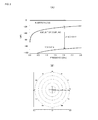
- Fig. 2 is a diagram illustrating the frequency characteristics and isolation characteristics of the directional coupler 120A.
- the insertion loss is approximately zero over the whole frequency range, and the amount of isolation of the isolation port ISO is extremely small compared with the amount of coupling of the coupling port CPL.
- the isolation characteristics illustrated in Fig. 2(B) illustrate, using polar coordinates, a signal output from the isolation port ISO, which is always approximately zero irrespective of the frequency.
- Patent Document 1 Japanese Unexamined Patent Application Publication No. 2009-044303
- the coupling factor of the mutual inductance M is 1, and a signal generated through electric field coupling and a signal generated through magnetic field coupling have opposite phases and cancel each other out at the isolation port ISO.
- the coupling factor of the mutual inductance M it is difficult to make the coupling factor of the mutual inductance M be 1 as described above, and usually there exists parasitic inductance generated due to routing lines or wiring lines.
- Fig. 3 is a diagram illustrating an influence from parasitic inductance in an actual directional coupler 120B.
- Fig. 3(A) illustrates the equivalent circuit of the directional coupler 120B.
- a parasitic inductance L1 is generated at the signal output port RFout of the main line 121
- a parasitic inductance L2 is generated at the coupling port CPL of the sub line 122.
- phase delays are generated in a signal generated through electric field coupling and a signal generated through magnetic field coupling in the sub line 122, whereby a signal that cannot be cancelled out by the sum of the two signals is generated in the isolation port ISO.
- sufficient isolation and directivity are not ensured.
- parasitic inductances may be generated also at the signal input port RFin and the isolation port ISO, but these inductances seldom degrade the isolation characteristics and directivity of the directional coupler, and hence it is assumed here that these inductances are not generated.
- series capacitors may be connected in series with the parasitic inductances L1 and L2, also in the case of the directional coupler 120B.
- Fig. 4 is a diagram illustrating a directional coupler 120C having a configuration in which series capacitors are connected in series with parasitic inductances.
- the isolation and directivity are improved at the frequency (approximately 2.0 GHz) at which the parasitic inductances and the series capacitors resonate in a series resonance mode.
- the device size of the whole directional coupler 120C is increased by the sizes of the series capacitors C1 and C2.
- the circuit needs to be designed in such a manner that the parasitic inductance L1 at the signal output port RFout is small and, in this case, the series capacitor C1 that resonates with the parasitic inductance L1 in a series resonance mode becomes extremely large.
- the device size is increased due to the series capacitor C1.
- the present invention relates to a transmission line type directional coupler.
- the directional coupler includes: a main line; and a sub line that is coupled to the main line through electric field coupling and magnetic field coupling.
- the main line includes a signal input port and a signal output port
- the sub line includes a coupling port and an isolation port.
- a series capacitor is connected to only one of the signal output port and the coupling port.
- a capacitance of the series capacitor is set smaller than or equal to the capacitance C1 or smaller than or equal to the capacitance C2.
- the isolation and directivity can be improved by inserting the series capacitor having the capacitance C1 or the capacitance C2, but improvement in the isolation and directivity increases as the capacitance becomes closer to the capacitance Cx, which is smaller than the capacitance C1 or the capacitance C2.
- the smaller the capacitance the smaller the size of the series capacitor, resulting in a reduction in device size.
- the series capacitor is preferably connected to only the coupling port among the signal output port and the coupling port.
- the main line, the sub line, and electrode patterns of the series capacitor are preferably formed using a thin-film process.
- At least one of the main line and the sub line is preferably used as an electrode for composing the series capacitor.
- the electrode, the main line, and the sub line that compose the series capacitor can be produced together and, hence, the number of processes added to the existing manufacturing processes can be decreased. Further, the device size is prevented from being increased by the size of an area occupied by the electrode of the series capacitor.
- the directional coupler described above preferably uses a semi-insulating substrate, resulting in a small loss and a reduction in the insertion loss of the directional coupler. In that case, reductions in device size and price can be realized by also mounting other active components together on the directional coupler.
- Fig. 5(A) is an equivalent circuit of a transmission line type directional coupler 20A according to a first embodiment of the present invention.
- the directional coupler 20A includes a main line 21 and a sub line 22.
- the main line 21 and the sub line 22 have respective inductances L, and are capacitively coupled to each other due to distributed capacitances C between the lines and coupled to each other through magnetic field coupling due to a mutual inductance M.
- the main line 21 has a signal input port RFin and a signal output port RFout.
- the sub line 22 has a coupling port CPL and an isolation port ISO.
- a signal due to electric field coupling and a signal due to magnetic field coupling have the same phase and strengthen each other at the coupling port CPL, and a signal due to electric field coupling and a signal due to magnetic field coupling have opposite phases and weaken each other at the isolation port ISO.
- the output of the coupling port CPL has only a +90° phase component with respect to the input power of the signal input port RFin. Further, the output of the isolation port ISO becomes approximately zero.
- the coupling factor of the mutual inductance M is not actually 1, and in the main line 21, there exists a parasitic inductance L1 due to the wiring and the like as well as the inductance L of the main line 21 itself. In the sub line 22, there exists a parasitic inductance L2 as well as the inductance of the inductance L of the sub line 22 itself.
- a series capacitor Cx is inserted in series with the parasitic inductance L2 in the sub line 22.
- the series capacitance Cx is made to be a capacitance which is obtained by connecting the series capacitor C1 in series with the series capacitor C2 provided in the directional coupler 120C described before (refer to Fig. 4 ).
- the series capacitance Cx satisfies the following equation. Note that the series capacitances C1 and C2 are capacitances respectively resonating with the parasitic inductances L1 and L2.
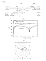
- Fig. 5(B) is a diagram illustrating the frequency characteristics of the directional coupler 20A
- Fig. 5(C) is a diagram illustrating the isolation characteristics using polar coordinates.
- the insertion loss at the signal output port RFout is substantially zero over the whole frequency range, and the isolation at the isolation port ISO is considerably improved by resonance at a frequency of approximately 2.0 GHz.
- the directivity which is the ratio of the amount of coupling to the amount of the isolation, is also considerably improved.
- the isolation characteristics and directivity can be improved by inserting the series capacitor Cx in series with the coupling port CPL.
- Fig. 6 illustrates comparisons of the directional coupler 20A with existing configurations in terms of frequency characteristics at a frequency of 2.0 GHz. Compared with the directional coupler 120A having an ideal configuration, the directional coupler 20A exhibits practically usable characteristics, since the isolation and directivity characteristics, although somewhat degraded, are sufficiently above 30 dB, which is a practical lower limit.
- the directional coupler 20A Compared with the directional coupler 120B, which is unfavorably influenced by a parasitic inductance, the directional coupler 20A exhibits improved isolation and directivity, and the directivity, in particular, is considerably improved in such a manner as to exceed 30 dB, which is a practical lower limit.
- the directional coupler 120C that includes the series capacitors C1 and C2 which resonate with the respective parasitic capacitances, an increase in device size is suppressed since only the single series capacitor Cx smaller than the series capacitors C1 and C2 is provided.
- the series capacitor Cx has a smaller capacitance and a smaller size than the series capacitors C1 and C2
- the directional coupler 20A is suitable for reduction in size also from this viewpoint. Consequently, in the directional coupler 20A in which the series capacitor Cx is connected in series with the coupling port CPL, an increase in device size can be significantly suppressed while avoiding an influence from the parasitic inductance.
- the parasitic inductance L1 is generated only at the signal output port RFout, it is preferable to provide the series capacitor C1 that resonates with the parasitic inductance L1 at the coupling port CPL.
- the parasitic inductance L2 is generated only at the coupling port CPL, it is preferable to provide the series capacitor C2 that resonates with the parasitic inductance L2 at the coupling port CPL.
- the isolation and directivity are improved also in these cases, similarly to the embodiment described above.
- the resonant frequency resulting from the use of the series capacitor Cx' shifts from a desired frequency (approximately 2.0 GHz).
- a desired frequency approximately 2.0 GHz.
- the effect of improvement in the isolation and directivity is limited and, hence, the isolation and directivity are expected to improve only to some extent.
- the device size is reduced by the size of the series capacitor C1, and degradation of the insertion loss due to insertion of the series capacitor C1 into the main line 21 is also suppressed.
- the resonant frequency resulting from the use of the series capacitor Cx is a desired frequency (approximately 2.0 GHz), and improvement in the isolation and directivity to some extent is expected.
- the device size is reduced by the size of the series capacitor C2.
- some degradation of the insertion loss is generated due to insertion of the series capacitor Cx into the main line 21.
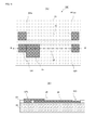
- FIG. 9(A) is a pattern diagram of a directional coupler 20D
- Fig. 9(B) illustrates a sectional view taken along line B-B' illustrated in Fig. 9(A) .
- the directional coupler 20D includes a main line 21, a sub line 22, a signal input port RFin, a signal output port RFout, a coupling port CPL, and an isolation port ISO formed on a semi-insulating substrate 24.
- a dielectric layer 23 having openings for exposing the ports is stacked on the semi-insulating substrate 24.
- An top electrode 25 is formed in the opening where the coupling port CPL is exposed and on the dielectric layer 23 in such a manner as to extend from the opening.
- a series capacitor Cx is formed by making the rectangular area of the end portion of the top electrode 25 overlap the rectangular area of the end portion of the sub line 22.
- the signal input port RFin, the signal output port RFout, the coupling port CPL, and the isolation port ISO are connected to external circuits using wiring lines or the like.
- Fig. 10 is a schematic diagram illustrating the process of manufacturing the directional coupler 20D.
- the directional coupler 20D which allows a plurality of devices to be arranged thereon, is manufactured using a wafer (substrate) made of a material with a low dielectric loss, such as gallium arsenide (GaAs).
- a wafer substrate
- GaAs gallium arsenide
- an area of the wafer in which an individual device is formed is illustrated as the semi-insulating substrate 24.
- the main line 21, the sub line 22, the signal input port RFin, the signal output port RFout, the coupling port CPL, and the isolation port ISO of the directional coupler 20D are formed on the semi-insulating substrate 24 using a thin-film process.
- the main line 21, the signal input port RFin, and the signal output port RFout are formed of Au or Al as an integral pattern so as to be electrically connected to one another.
- the sub line 22 and the isolation port ISO are also formed of Au or Al as an integral pattern so as to be electrically connected to each other.
- the coupling port CPL is formed of Au or Al as a pattern spaced apart from the sub line 22.
- a resist layer is formed using a photolithography process or the like, and an unnecessary electrode material is removed by etching.
- an electrode material is deposited in portions other than the resist layer pattern using evaporation, sputtering, plating, or the like, and finally the resist layer is lifted off, whereby electrode patterns are formed.
- silicon is generally used as a substrate material.
- a silicon substrate which is a semiconductor substrate and has a large loss
- the directional coupler of the present invention insertion loss in the main line increases.
- the semi-insulating substrate 24 which is formed of a low-loss material such as GaAs, the insertion loss can be reduced.
- the dielectric layer 23 is formed on the semi-insulating substrate 24 in such a manner that four openings are provided in the dielectric layer 23 for exposing the signal input port RFin, the signal output port RFout, the coupling port CPL, and the isolation port ISO.
- An etching process may be used to form the openings.
- the top electrode 25 is formed on the surface of the dielectric layer 23 using a thin-film process.
- the top electrode 25 is formed as a pattern in such a manner as to extend from the opening where the coupling port CPL is exposed to the rectangular area of an end of the sub line 22.
- a region in which the top electrode 25 and the sub line 22 face each other can be made to function as the series capacitor Cx, whereby the isolation and directivity of the directional coupler 20D can be improved.
- Fig. 11(A) a pattern diagram of a directional coupler 20E
- Fig. 11(B) illustrates a sectional view taken along line B-B' illustrated in Fig. 11(A)
- the rectangular region functioning as the series capacitor Cx is enlarged so as to have a shape with a larger area than the surrounding portion. With this configuration, the capacitance of the series capacitor Cx can be made relatively large.
- Fig. 12(A) is a pattern diagram of a directional coupler 20F
- Fig. 12(B) illustrates a sectional view taken along line B-B' illustrated in Fig. 12(A)
- the top electrode 25 is shaped like a line which overlaps the sub line 22, while the shape of the sub line 22 is maintained as it is, whereby the rectangular region which functions as the series capacitor Cx is made to have a large area. With this configuration, the capacitance of the series capacitor Cx can be ensured without increasing the device size.
- the present invention can be realized using various configurations, and the scope of the present invention is not limited to the embodiments described above.
- the scope of the present invention is described by the Claims, and it is to be understood that the present invention includes all the modifications that are within the scope, or its equivalent, of the present invention.
Landscapes
- Microwave Amplifiers (AREA)
- Transmitters (AREA)
- Near-Field Transmission Systems (AREA)
Abstract
Description
- The present invention relates to directional couplers, and specifically relates to improvement of the characteristics of transmission line type directional couplers.
- To date, directional couplers have been used for, for example, measurement of high-frequency signals (refer to, for example, Patent Document 1).
-
Fig. 1(A) is a block diagram of anRF transmission circuit 100 used in, for example, cellular phones. TheRF transmission circuit 100 includes anantenna 111, adirectional coupler 120A, atransmission power amplifier 113, amodulation circuit 112, and an automaticgain control circuit 114. Thedirectional coupler 120A, which is of a transmission line type, includes amain line 121 and a coupling line (sub line) 122. Themain line 121 is connected between theantenna 111 and thetransmission power amplifier 113. The automaticgain control circuit 114 is connected to thedirectional coupler 120A and thesub line 122, and controls thetransmission power amplifier 113 on the basis of a signal from thesub line 122 which is coupled to themain line 121. -
Fig. 1(B) is an equivalent circuit diagram of thedirectional coupler 120A. Here, thedirectional coupler 120A is assumed to be an ideal circuit, in which the coupling factor of a mutual inductance M between themain line 121 and thesub line 122 is 1. Themain line 121 has a signal input port RFin and a signal output port RFout, and thesub line 122 has a coupling port CPL and an isolation port ISO. Themain line 121 and thesub line 122 are coupled to each other through electric field coupling due to distributed capacitances C between the two lines, and at the same time coupled to each other through magnetic field coupling due to the mutual inductance M. - When a signal S1 is input from the signal input port RFin in the
main line 121, a signal S2 propagates toward the coupling port CPL and a signal S3 propagates toward the isolation port ISO, in thesub line 22, due to electric field coupling caused by coupling capacitances C. A signal S4 and a signal S5 propagate in a direction from the isolation port ISO to the coupling port CPL in a closed loop formed of thesub line 22 and the ground (GND), due to magnetic field coupling caused by the mutual inductance M. - In this ideal equivalent circuit, the signal S2 and the signal S4 that flow to the coupling port CPL both have a phase of +90° with respect to the signal S1, i.e., the same phase. Hence, a signal having a power which is the sum of the power of the signal S2 and the power of the signal S4 is output from the coupling port CPL. On the other hand, regarding the signals S3 and S5 that flow to and from the isolation port ISO, the signal S3 has a phase of +90° with respect to the signal S1, and the signal S5 has a phase of - 90° with respect to the signal S1, that is, the signal S3 and the signal S5 have opposite phases. Hence, the power of the signal S3 and the power of the signal S5 cancel each other out, whereby no signals are output.
-
Fig. 2 is a diagram illustrating the frequency characteristics and isolation characteristics of thedirectional coupler 120A. Referring to the frequency characteristics illustrated inFig. 2(A) , the insertion loss is approximately zero over the whole frequency range, and the amount of isolation of the isolation port ISO is extremely small compared with the amount of coupling of the coupling port CPL. Hence, a high directivity is obtained. The isolation characteristics illustrated inFig. 2(B) illustrate, using polar coordinates, a signal output from the isolation port ISO, which is always approximately zero irrespective of the frequency. - Patent Document 1: Japanese Unexamined Patent Application Publication No.
2009-044303 - In the ideal
directional coupler 120A described above, the coupling factor of the mutual inductance M is 1, and a signal generated through electric field coupling and a signal generated through magnetic field coupling have opposite phases and cancel each other out at the isolation port ISO. However, in an actual directional coupler, it is difficult to make the coupling factor of the mutual inductance M be 1 as described above, and usually there exists parasitic inductance generated due to routing lines or wiring lines. -
Fig. 3 is a diagram illustrating an influence from parasitic inductance in an actualdirectional coupler 120B.Fig. 3(A) illustrates the equivalent circuit of thedirectional coupler 120B. In thedirectional coupler 120B, a parasitic inductance L1 is generated at the signal output port RFout of themain line 121, and a parasitic inductance L2 is generated at the coupling port CPL of thesub line 122.Fig. 3(B) and Fig. 3(C) respectively illustrate the frequency characteristics and isolation characteristics of thedirectional coupler 120B for the case in which the parasitic inductance L1 = 0.5 nH and the parasitic inductance L2 = 1.0 nH. In this case, phase delays are generated in a signal generated through electric field coupling and a signal generated through magnetic field coupling in thesub line 122, whereby a signal that cannot be cancelled out by the sum of the two signals is generated in the isolation port ISO. As a result, sufficient isolation and directivity are not ensured. Note that parasitic inductances may be generated also at the signal input port RFin and the isolation port ISO, but these inductances seldom degrade the isolation characteristics and directivity of the directional coupler, and hence it is assumed here that these inductances are not generated. - Connecting a series capacitor in series with a parasitic inductance is a known technique to suppress an influence from parasitic inductance in a high-frequency circuit. Hence, series capacitors may be connected in series with the parasitic inductances L1 and L2, also in the case of the
directional coupler 120B. -
Fig. 4 is a diagram illustrating adirectional coupler 120C having a configuration in which series capacitors are connected in series with parasitic inductances. In thedirectional coupler 120C, a series capacitor C1 having a capacitance C1 (= 14 pF) that resonates in a series resonance mode with the inductance L1 (= 0.5 nH) at a desired frequency (approximately 2.0 GHz) is inserted into themain line 121, and a series capacitor C2 having a capacitance C2 (= 6 pF) that resonates in a series resonance mode with the inductance L2 (= 1.0 nH) at the desired frequency (approximately 2.0 GHz) is inserted into thesub line 122. In this case, the isolation and directivity are improved at the frequency (approximately 2.0 GHz) at which the parasitic inductances and the series capacitors resonate in a series resonance mode. - However, with such a circuit configuration in which series capacitors are inserted, the device size of the whole
directional coupler 120C is increased by the sizes of the series capacitors C1 and C2. In particular, from the view point of impedance matching with an external circuit at the signal output port RFout, the circuit needs to be designed in such a manner that the parasitic inductance L1 at the signal output port RFout is small and, in this case, the series capacitor C1 that resonates with the parasitic inductance L1 in a series resonance mode becomes extremely large. Hence, the device size is increased due to the series capacitor C1. - Accordingly, it is an object of the present invention to provide a directional coupler having a configuration in which, even when a parasitic inductance exists, good isolation characteristics are obtained and an increase in the size of the directional coupler is suppressed. Solution to Problem
- The present invention relates to a transmission line type directional coupler. The directional coupler includes: a main line; and a sub line that is coupled to the main line through electric field coupling and magnetic field coupling. The main line includes a signal input port and a signal output port, and the sub line includes a coupling port and an isolation port. Here, a series capacitor is connected to only one of the signal output port and the coupling port.
- With this configuration, by connecting a series capacitor to only one of the signal output port and the coupling port, the isolation and directivity can be improved, and an increase in device size is suppressed compared with the case in which a series capacitor is connected to both of the signal output port and the coupling port.
- Preferably, in the directional coupler described above, for a capacitance C1 that resonates with a parasitic inductance of the signal output port at a desired frequency and for a capacitance C2 that resonates with a parasitic inductance of the coupling port at the desired frequency, a capacitance of the series capacitor is set smaller than or equal to the capacitance C1 or smaller than or equal to the capacitance C2. More preferably, the capacitance of the series capacitor is set to a capacitance Cx that satisfies the following equation:

The isolation and directivity can be improved by inserting the series capacitor having the capacitance C1 or the capacitance C2, but improvement in the isolation and directivity increases as the capacitance becomes closer to the capacitance Cx, which is smaller than the capacitance C1 or the capacitance C2. Further, the smaller the capacitance, the smaller the size of the series capacitor, resulting in a reduction in device size. - In the directional coupler described above, the series capacitor is preferably connected to only the coupling port among the signal output port and the coupling port. With this configuration, since the series capacitor is not connected to the signal output port, an increase in insertion loss can be prevented.
- In the directional coupler described above, the main line, the sub line, and electrode patterns of the series capacitor are preferably formed using a thin-film process. By forming the directional coupler using a thin-film process, variations in the positions of the components can be suppressed, whereby variations in the electric characteristics of the directional coupler can be limited to very small variations.
- In the directional coupler described above, at least one of the main line and the sub line is preferably used as an electrode for composing the series capacitor. With this configuration, the electrode, the main line, and the sub line that compose the series capacitor can be produced together and, hence, the number of processes added to the existing manufacturing processes can be decreased. Further, the device size is prevented from being increased by the size of an area occupied by the electrode of the series capacitor.
- The directional coupler described above preferably uses a semi-insulating substrate, resulting in a small loss and a reduction in the insertion loss of the directional coupler. In that case, reductions in device size and price can be realized by also mounting other active components together on the directional coupler.
- According to the present invention, even when parasitic inductance exists in the main line or sub line, good isolation characteristics and directivity can be obtained by inserting a series capacitor at only one of the signal output port and coupling port. In that case, an increase in the device size can be suppressed since only one series capacitor is used instead of two series capacitors. Brief Description of Drawings
-
- [
Fig. 1] Fig. 1 is a diagram illustrating a transmission line type directional coupler provided in an RF transmission circuit. - [
Fig. 2] Fig. 2 is a diagram illustrating the frequency characteristics and isolation characteristics of the directional coupler illustrated inFig. 1 . - [
Fig. 3] Fig. 3 is a diagram illustrating an influence from a parasitic inductance in a transmission line type directional coupler. - [
Fig. 4] Fig. 4 is a diagram illustrating an influence from a series capacitance that resonates with a parasitic inductance in a transmission line type directional coupler. - [
Fig. 5] Fig. 5 is a diagram illustrating a directional coupler according to a first embodiment of the present invention. - [
Fig. 6] Fig. 6 illustrates comparisons of a configuration in the present invention and existing configurations in terms of frequency characteristics. - [
Fig. 7] Fig. 7 is a diagram illustrating a directional coupler according to a second embodiment of the present invention. - [
Fig. 8] Fig. 8 is a diagram illustrating a directional coupler according to a third embodiment of the present invention. - [
Fig. 9] Fig. 9 is a diagram illustrating an example of a directional coupler. - [
Fig. 10] Fig. 10 is a diagram illustrating an example of a thin-film process related to the manufacturing of a directional coupler. - [
Fig. 11] Fig. 11 is a diagram illustrating another example of a directional coupler. - [
Fig. 12] Fig. 12 is a diagram illustrating still another example of a directional coupler. - Hereinafter, the general configuration and operation of a transmission line type directional coupler according to an embodiment of the present invention will be described.
-
Fig. 5(A) is an equivalent circuit of a transmission line typedirectional coupler 20A according to a first embodiment of the present invention. - The
directional coupler 20A includes amain line 21 and asub line 22. Themain line 21 and thesub line 22 have respective inductances L, and are capacitively coupled to each other due to distributed capacitances C between the lines and coupled to each other through magnetic field coupling due to a mutual inductance M. Themain line 21 has a signal input port RFin and a signal output port RFout. Thesub line 22 has a coupling port CPL and an isolation port ISO. In thesub line 22, a signal due to electric field coupling and a signal due to magnetic field coupling have the same phase and strengthen each other at the coupling port CPL, and a signal due to electric field coupling and a signal due to magnetic field coupling have opposite phases and weaken each other at the isolation port ISO. - In the case of ideal directional coupling, by appropriately adjusting the mutual inductance M and the distributed capacitances C, the output of the coupling port CPL has only a +90° phase component with respect to the input power of the signal input port RFin. Further, the output of the isolation port ISO becomes approximately zero. However, the coupling factor of the mutual inductance M is not actually 1, and in the
main line 21, there exists a parasitic inductance L1 due to the wiring and the like as well as the inductance L of themain line 21 itself. In thesub line 22, there exists a parasitic inductance L2 as well as the inductance of the inductance L of thesub line 22 itself. - As a result, a phase delay caused by a parasitic inductance is generated between the signal due to magnetic field coupling and the signal due to electric field coupling generated in the
sub line 22. Hence the output powers due to electric field coupling and magnetic field coupling cannot be completely cancelled out at the isolation port ISO, causing degradation of the isolation characteristics. - Hence, in the present embodiment, a series capacitor Cx is inserted in series with the parasitic inductance L2 in the
sub line 22. Here, the series capacitance Cx is made to be a capacitance which is obtained by connecting the series capacitor C1 in series with the series capacitor C2 provided in thedirectional coupler 120C described before (refer toFig. 4 ). In other words, the series capacitance Cx satisfies the following equation. Note that the series capacitances C1 and C2 are capacitances respectively resonating with the parasitic inductances L1 and L2.
As a result, in thedirectional coupler 20A, the isolation and directivity at a desired frequency (approximately 2.0 GHz) are improved even though the parasitic inductances L1 and L2 exist.Fig. 5(B) is a diagram illustrating the frequency characteristics of thedirectional coupler 20A, andFig. 5(C) is a diagram illustrating the isolation characteristics using polar coordinates. In the frequency characteristics of thedirectional coupler 20A, the insertion loss at the signal output port RFout is substantially zero over the whole frequency range, and the isolation at the isolation port ISO is considerably improved by resonance at a frequency of approximately 2.0 GHz. At a frequency of approximately 2.0 GHz, the directivity, which is the ratio of the amount of coupling to the amount of the isolation, is also considerably improved. - In this manner, in the
directional coupler 20A, the isolation characteristics and directivity can be improved by inserting the series capacitor Cx in series with the coupling port CPL.Fig. 6 illustrates comparisons of thedirectional coupler 20A with existing configurations in terms of frequency characteristics at a frequency of 2.0 GHz. Compared with thedirectional coupler 120A having an ideal configuration, thedirectional coupler 20A exhibits practically usable characteristics, since the isolation and directivity characteristics, although somewhat degraded, are sufficiently above 30 dB, which is a practical lower limit. Compared with thedirectional coupler 120B, which is unfavorably influenced by a parasitic inductance, thedirectional coupler 20A exhibits improved isolation and directivity, and the directivity, in particular, is considerably improved in such a manner as to exceed 30 dB, which is a practical lower limit. Compared with thedirectional coupler 120C that includes the series capacitors C1 and C2 which resonate with the respective parasitic capacitances, an increase in device size is suppressed since only the single series capacitor Cx smaller than the series capacitors C1 and C2 is provided. Further, since the series capacitor Cx has a smaller capacitance and a smaller size than the series capacitors C1 and C2, thedirectional coupler 20A is suitable for reduction in size also from this viewpoint. Consequently, in thedirectional coupler 20A in which the series capacitor Cx is connected in series with the coupling port CPL, an increase in device size can be significantly suppressed while avoiding an influence from the parasitic inductance. - Note that in the case where the parasitic inductance L1 is generated only at the signal output port RFout, it is preferable to provide the series capacitor C1 that resonates with the parasitic inductance L1 at the coupling port CPL. In the case where the parasitic inductance L2 is generated only at the coupling port CPL, it is preferable to provide the series capacitor C2 that resonates with the parasitic inductance L2 at the coupling port CPL. The isolation and directivity are improved also in these cases, similarly to the embodiment described above.
- A
directional coupler 20B according to a second embodiment will now be described.Fig. 7(A) is an equivalent circuit diagram of thedirectional coupler 20B, which has a configuration in which a series capacitor Cx' having a capacitance Cx' (= C2 = 6pF) is inserted only at the coupling port CPL. - With this configuration, as illustrated by the frequency characteristics and isolation characteristics of
Figs. 7(B) and 7(C) , the resonant frequency resulting from the use of the series capacitor Cx' shifts from a desired frequency (approximately 2.0 GHz). As a result, the effect of improvement in the isolation and directivity is limited and, hence, the isolation and directivity are expected to improve only to some extent. However, since at least the series capacitor C1 provided at the signal output port RFout is omitted, the device size is reduced by the size of the series capacitor C1, and degradation of the insertion loss due to insertion of the series capacitor C1 into themain line 21 is also suppressed. Hence, it is thought to be preferable to connect the capacitor Cx which is equivalent to the series capacitor C1 and the series capacitor C2 connected in series to each other, as in thedirectional coupler 20A. - A directional coupler 20C according to a third embodiment will now be described.
Fig. 8(A) is an equivalent circuit diagram of the directional coupler 20C, which has a configuration in which the series capacitor Cx having the capacitance Cx (= 4.2 pF) is connected to only the signal output port RFout. - With this configuration, as illustrated by the frequency characteristics and isolation characteristics of
Figs. 8(B) and 8(C) , the resonant frequency resulting from the use of the series capacitor Cx is a desired frequency (approximately 2.0 GHz), and improvement in the isolation and directivity to some extent is expected. Further, since at least the series capacitor C2 provided at the coupling port CPL is omitted, the device size is reduced by the size of the series capacitor C2. However, some degradation of the insertion loss is generated due to insertion of the series capacitor Cx into themain line 21. As a result, it is thought to be preferable to connect a series capacitor to the coupling port CPL as in thedirectional coupler 20A. - A method of manufacturing a directional coupler of the present invention will now be described.
Fig. 9(A) is a pattern diagram of adirectional coupler 20D, andFig. 9(B) illustrates a sectional view taken along line B-B' illustrated inFig. 9(A) . - The
directional coupler 20D includes amain line 21, asub line 22, a signal input port RFin, a signal output port RFout, a coupling port CPL, and an isolation port ISO formed on asemi-insulating substrate 24. Adielectric layer 23 having openings for exposing the ports is stacked on thesemi-insulating substrate 24. Antop electrode 25 is formed in the opening where the coupling port CPL is exposed and on thedielectric layer 23 in such a manner as to extend from the opening. A series capacitor Cx is formed by making the rectangular area of the end portion of thetop electrode 25 overlap the rectangular area of the end portion of thesub line 22. The signal input port RFin, the signal output port RFout, the coupling port CPL, and the isolation port ISO are connected to external circuits using wiring lines or the like. -
Fig. 10 is a schematic diagram illustrating the process of manufacturing thedirectional coupler 20D. - The
directional coupler 20D, which allows a plurality of devices to be arranged thereon, is manufactured using a wafer (substrate) made of a material with a low dielectric loss, such as gallium arsenide (GaAs). In the figure, an area of the wafer in which an individual device is formed is illustrated as thesemi-insulating substrate 24. - First, as illustrated in
Fig. 10(B) , themain line 21, thesub line 22, the signal input port RFin, the signal output port RFout, the coupling port CPL, and the isolation port ISO of thedirectional coupler 20D are formed on thesemi-insulating substrate 24 using a thin-film process. Note that themain line 21, the signal input port RFin, and the signal output port RFout are formed of Au or Al as an integral pattern so as to be electrically connected to one another. Thesub line 22 and the isolation port ISO are also formed of Au or Al as an integral pattern so as to be electrically connected to each other. The coupling port CPL is formed of Au or Al as a pattern spaced apart from thesub line 22. - In the thin-film process, after an electrode material has been formed over the whole surface using evaporation, sputtering, plating, or the like, a resist layer is formed using a photolithography process or the like, and an unnecessary electrode material is removed by etching. Alternatively, after a resist layer pattern has been first formed using a photolithography process, an electrode material is deposited in portions other than the resist layer pattern using evaporation, sputtering, plating, or the like, and finally the resist layer is lifted off, whereby electrode patterns are formed. By using such a thin-film process, variations in the positions of the electrodes can be suppressed to 10 µm or less and, hence, variations in the electrical characteristics of the directional coupler can be made very small, whereby the yield of the directional coupler can be increased.
- Note that when devices are manufactured using a thin-film process, silicon is generally used as a substrate material. However, when a silicon substrate, which is a semiconductor substrate and has a large loss, is used in the directional coupler of the present invention, insertion loss in the main line increases. On the other hand, by using the
semi-insulating substrate 24, which is formed of a low-loss material such as GaAs, the insertion loss can be reduced. - Then, as illustrated in
Fig. 10(C) , thedielectric layer 23 is formed on thesemi-insulating substrate 24 in such a manner that four openings are provided in thedielectric layer 23 for exposing the signal input port RFin, the signal output port RFout, the coupling port CPL, and the isolation port ISO. An etching process may be used to form the openings. - Then, as illustrated in
Fig. 10(D) , thetop electrode 25 is formed on the surface of thedielectric layer 23 using a thin-film process. Thetop electrode 25 is formed as a pattern in such a manner as to extend from the opening where the coupling port CPL is exposed to the rectangular area of an end of thesub line 22. As a result, a region in which thetop electrode 25 and thesub line 22 face each other can be made to function as the series capacitor Cx, whereby the isolation and directivity of thedirectional coupler 20D can be improved. - Another example of the directional coupler of the present invention will now be described.
Fig. 11(A) a pattern diagram of adirectional coupler 20E, andFig. 11(B) illustrates a sectional view taken along line B-B' illustrated inFig. 11(A) . In thesub line 22 and thetop electrode 25 of thedirectional coupler 20E, the rectangular region functioning as the series capacitor Cx is enlarged so as to have a shape with a larger area than the surrounding portion. With this configuration, the capacitance of the series capacitor Cx can be made relatively large. - Still another example of the directional coupler of the present invention will now be described.
Fig. 12(A) is a pattern diagram of adirectional coupler 20F, andFig. 12(B) illustrates a sectional view taken along line B-B' illustrated inFig. 12(A) . In thedirectional coupler 20F, to ensure that the series capacitor Cx has a relatively large capacitance, thetop electrode 25 is shaped like a line which overlaps thesub line 22, while the shape of thesub line 22 is maintained as it is, whereby the rectangular region which functions as the series capacitor Cx is made to have a large area. With this configuration, the capacitance of the series capacitor Cx can be ensured without increasing the device size. - As described in the embodiments and examples above, the present invention can be realized using various configurations, and the scope of the present invention is not limited to the embodiments described above. The scope of the present invention is described by the Claims, and it is to be understood that the present invention includes all the modifications that are within the scope, or its equivalent, of the present invention.
-
- CPL:
- coupling port
- ISO:
- isolation port
- RFin:
- signal input port
- RFout:
- signal output port
- 20A-20F:
- directional couplers
- 21:
- main line
- 22:
- sub line
- 23:
- dielectric layer
- 24:
- semi-insulating substrate
- 25:
- top electrode
Claims (7)
- A directional coupler comprising:a main line including a signal input port and a signal output port; anda sub line that includes a coupling port and an isolation port and that is coupled to the main line through electric field coupling and magnetic field coupling,wherein a series capacitor is connected to only one of the signal output port and the coupling port.
- The directional coupler according to Claim 1, wherein for a capacitance C1 that resonates with a parasitic inductance of the signal output port at a desired frequency and for a capacitance C2 that resonates with a parasitic inductance of the coupling port at the desired frequency, a capacitance of the series capacitor is set smaller than or equal to the capacitance C1 or smaller than or equal to the capacitance C2.
- The directional coupler according to Claim 2, wherein for the capacitance C1 that resonates with the parasitic inductance of the signal output port at the desired frequency and for the capacitance C2 that resonates with the parasitic inductance of the coupling port at the desired frequency, the capacitance of the series capacitor is set to a capacitance Cx that satisfies the following equation:

- The directional coupler according to any one of Claims 1 to 3, wherein the series capacitor is connected to only the coupling port among the signal output port and the coupling port.
- The directional coupler according to any one of Claims 1 to 4, wherein the main line, the sub line, and electrode patterns of the series capacitor are formed using a thin-film process.
- The directional coupler according to any one of Claims 1 to 5, wherein at least one of the main line and the sub line is used as an electrode for composing the series capacitor.
- The directional coupler according to any one of Claims 1 to 6, further comprising a semi-insulating substrate on which the main line, the sub line, and electrodes for composing the series capacitor are formed.
Applications Claiming Priority (2)
| Application Number | Priority Date | Filing Date | Title |
|---|---|---|---|
| JP2010253854 | 2010-11-12 | ||
| PCT/JP2011/075895 WO2012063887A1 (en) | 2010-11-12 | 2011-11-10 | Directional coupler |
Publications (2)
| Publication Number | Publication Date |
|---|---|
| EP2639877A1 true EP2639877A1 (en) | 2013-09-18 |
| EP2639877A4 EP2639877A4 (en) | 2017-12-27 |
Family
ID=46051024
Family Applications (1)
| Application Number | Title | Priority Date | Filing Date |
|---|---|---|---|
| EP11840244.5A Withdrawn EP2639877A4 (en) | 2010-11-12 | 2011-11-10 | Directional coupler |
Country Status (6)
| Country | Link |
|---|---|
| US (1) | US8803633B2 (en) |
| EP (1) | EP2639877A4 (en) |
| JP (1) | JP5633574B2 (en) |
| KR (1) | KR101440369B1 (en) |
| CN (1) | CN103201899B (en) |
| WO (1) | WO2012063887A1 (en) |
Families Citing this family (22)
| Publication number | Priority date | Publication date | Assignee | Title |
|---|---|---|---|---|
| US9287624B2 (en) * | 2013-10-21 | 2016-03-15 | Hong Kong Applied Science and Technology Research Institute Company Limited | Antenna circuit and a method of optimisation thereof |
| JP6660892B2 (en) | 2014-06-12 | 2020-03-11 | スカイワークス ソリューションズ, インコーポレイテッドSkyworks Solutions, Inc. | Devices and methods related to directional couplers |
| JP6210029B2 (en) * | 2014-07-23 | 2017-10-11 | 株式会社村田製作所 | Directional coupler |
| US9496902B2 (en) | 2014-07-24 | 2016-11-15 | Skyworks Solutions, Inc. | Apparatus and methods for reconfigurable directional couplers in an RF transceiver with selectable phase shifters |
| TWI720014B (en) | 2015-09-10 | 2021-03-01 | 美商西凱渥資訊處理科技公司 | Electromagnetic couplers for multi-frequency power detection and system having the same |
| CN105226368B (en) * | 2015-11-12 | 2017-12-15 | 无锡中普微电子有限公司 | Braodband directional coupler |
| WO2017136631A1 (en) | 2016-02-05 | 2017-08-10 | Skyworks Solutions, Inc. | Electromagnetic couplers with multi-band filtering |
| TWI720128B (en) | 2016-02-29 | 2021-03-01 | 美商天工方案公司 | Integrated filter and directional coupler assemblies |
| KR20180121791A (en) * | 2016-03-30 | 2018-11-08 | 스카이워크스 솔루션즈, 인코포레이티드 | Adjustable active silicon for improved coupler linearity and reconfiguration |
| WO2017189824A1 (en) | 2016-04-29 | 2017-11-02 | Skyworks Solutions, Inc. | Compensated electromagnetic coupler |
| TW201739099A (en) | 2016-04-29 | 2017-11-01 | 天工方案公司 | Tunable electromagnetic coupler and modules and devices using same |
| CN109417215B (en) | 2016-05-09 | 2021-08-24 | 天工方案公司 | Self-regulating electromagnetic coupler with automatic frequency detection |
| US10164681B2 (en) | 2016-06-06 | 2018-12-25 | Skyworks Solutions, Inc. | Isolating noise sources and coupling fields in RF chips |
| CN109565292B (en) | 2016-06-22 | 2021-02-05 | 天工方案公司 | Electromagnetic coupler device for multi-frequency power detection and apparatus containing the same |
| CN106207363A (en) * | 2016-08-30 | 2016-12-07 | 宇龙计算机通信科技(深圳)有限公司 | A kind of directional coupler |
| TWI628844B (en) * | 2016-08-31 | 2018-07-01 | 璟德電子工業股份有限公司 | Miniature directional coupler |
| US10742189B2 (en) | 2017-06-06 | 2020-08-11 | Skyworks Solutions, Inc. | Switched multi-coupler apparatus and modules and devices using same |
| WO2020185560A1 (en) * | 2019-03-13 | 2020-09-17 | Avx Corporation | Compact thin film surface mountable coupler having wide-band performance |
| CN111817684B (en) * | 2020-07-15 | 2023-06-06 | 武汉博畅通信设备有限责任公司 | Magnetic core type 3dB electric bridge |
| DE102022201807A1 (en) | 2021-02-23 | 2022-08-25 | Skyworks Solutions, Inc. | INTELLIGENT BIDIRECTIONAL COUPLER WITH SWITCHABLE INDUCTORS |
| US12057611B2 (en) | 2021-06-02 | 2024-08-06 | Skyworks Solutions, Inc. | Directional coupler with multiple arrangements of termination |
| CN114865265B (en) * | 2022-06-14 | 2023-02-21 | 江南大学 | Broadband low-loss directional coupler and frequency modulation transmitter system |
Family Cites Families (17)
| Publication number | Priority date | Publication date | Assignee | Title |
|---|---|---|---|---|
| US4795989A (en) * | 1988-02-11 | 1989-01-03 | Honeywell, Inc. | MMW microstrip coupler having movable test probe |
| JP2651336B2 (en) | 1993-06-07 | 1997-09-10 | 株式会社エイ・ティ・アール光電波通信研究所 | Directional coupler |
| JPH08307286A (en) * | 1995-04-28 | 1996-11-22 | Taise:Kk | Power controller |
| US6342681B1 (en) * | 1997-10-15 | 2002-01-29 | Avx Corporation | Surface mount coupler device |
| JP3744249B2 (en) * | 1999-03-29 | 2006-02-08 | 株式会社村田製作所 | Transmission output control device and wireless device using the same |
| US7327582B2 (en) * | 2000-09-21 | 2008-02-05 | Ultrasource, Inc. | Integrated thin film capacitor/inductor/interconnect system and method |
| JP2002223135A (en) * | 2001-01-29 | 2002-08-09 | Tdk Corp | High frequency amplifier and high frequency output circuit using the same |
| US6825738B2 (en) * | 2002-12-18 | 2004-11-30 | Analog Devices, Inc. | Reduced size microwave directional coupler |
| JP2006333290A (en) * | 2005-05-30 | 2006-12-07 | Fujitsu Ltd | Monitor circuit |
| JP4599302B2 (en) * | 2006-01-18 | 2010-12-15 | 株式会社ケンウッド | Directional coupler |
| JP5081237B2 (en) * | 2006-07-06 | 2012-11-28 | ジ・オハイオ・ステイト・ユニバーシティ・リサーチ・ファウンデイション | Emulation of anisotropic media in transmission lines |
| JP2009044303A (en) | 2007-08-07 | 2009-02-26 | Panasonic Corp | Attenuator composite coupler |
| FR2933540B1 (en) * | 2008-07-01 | 2011-12-02 | St Microelectronics Tours Sas | INTEGRATED DIRECTIVE COUPLER |
| JP5169844B2 (en) | 2009-01-06 | 2013-03-27 | 三菱電機株式会社 | Directional coupler |
| US7961064B2 (en) | 2009-01-30 | 2011-06-14 | Tdk Corporation | Directional coupler including impedance matching and impedance transforming attenuator |
| CN201509200U (en) * | 2009-06-22 | 2010-06-16 | 摩比天线技术(深圳)有限公司 | Directional coupler and signal detection system |
| WO2011102187A1 (en) * | 2010-02-19 | 2011-08-25 | 株式会社村田製作所 | Directional coupler |
-
2011
- 2011-11-10 KR KR1020137011119A patent/KR101440369B1/en active Active
- 2011-11-10 JP JP2012542969A patent/JP5633574B2/en active Active
- 2011-11-10 CN CN201180054132.7A patent/CN103201899B/en active Active
- 2011-11-10 EP EP11840244.5A patent/EP2639877A4/en not_active Withdrawn
- 2011-11-10 WO PCT/JP2011/075895 patent/WO2012063887A1/en not_active Ceased
-
2013
- 2013-05-09 US US13/891,075 patent/US8803633B2/en active Active
Non-Patent Citations (1)
| Title |
|---|
| See references of WO2012063887A1 * |
Also Published As
| Publication number | Publication date |
|---|---|
| WO2012063887A1 (en) | 2012-05-18 |
| US8803633B2 (en) | 2014-08-12 |
| CN103201899B (en) | 2015-01-21 |
| JP5633574B2 (en) | 2014-12-03 |
| JPWO2012063887A1 (en) | 2014-05-12 |
| CN103201899A (en) | 2013-07-10 |
| EP2639877A4 (en) | 2017-12-27 |
| US20130241668A1 (en) | 2013-09-19 |
| KR20130093635A (en) | 2013-08-22 |
| KR101440369B1 (en) | 2014-09-15 |
Similar Documents
| Publication | Publication Date | Title |
|---|---|---|
| EP2639877A1 (en) | Directional coupler | |
| CN106505962B (en) | Impedance matching device with coupled resonator structure | |
| EP2822091B1 (en) | Directional coupler | |
| US7710338B2 (en) | Slot antenna apparatus eliminating unstable radiation due to grounding structure | |
| US8421553B2 (en) | Directional coupler | |
| US11121444B2 (en) | Directional coupler | |
| US7696929B2 (en) | Tunable microstrip devices | |
| EP2515435B1 (en) | Power amplifier | |
| US20040155729A1 (en) | Multi-bit phase shifter and manufacturing method thereof | |
| JP2013183351A (en) | Directional coupler | |
| US9362604B2 (en) | RF planar filter having resonator segments connected by adjustable electrical links | |
| JPH11274411A (en) | Microwave / millimeter wave circuit device and manufacturing method thereof | |
| US7342469B2 (en) | Air cavity module for planar type filter operating in millimeter-wave frequency bands | |
| JP4189971B2 (en) | Variable frequency type high frequency filter | |
| TW202308218A (en) | Dielectric resonator, and dielectric filter and multiplexer using same | |
| JP7658465B2 (en) | Power Amplifiers | |
| US7276981B2 (en) | 3D MMIC VCO and methods of making the same | |
| KR20070075936A (en) | SIR Type Band Pass Filter | |
| US12519429B2 (en) | High frequency amplifier | |
| Hettak et al. | High-performance 3D on-chip air-gap spiral inductor and its application to filter design |
Legal Events
| Date | Code | Title | Description |
|---|---|---|---|
| PUAI | Public reference made under article 153(3) epc to a published international application that has entered the european phase |
Free format text: ORIGINAL CODE: 0009012 |
|
| 17P | Request for examination filed |
Effective date: 20130507 |
|
| AK | Designated contracting states |
Kind code of ref document: A1 Designated state(s): AL AT BE BG CH CY CZ DE DK EE ES FI FR GB GR HR HU IE IS IT LI LT LU LV MC MK MT NL NO PL PT RO RS SE SI SK SM TR |
|
| DAX | Request for extension of the european patent (deleted) | ||
| RA4 | Supplementary search report drawn up and despatched (corrected) |
Effective date: 20171128 |
|
| RIC1 | Information provided on ipc code assigned before grant |
Ipc: H01P 5/18 20060101AFI20171122BHEP |
|
| STAA | Information on the status of an ep patent application or granted ep patent |
Free format text: STATUS: EXAMINATION IS IN PROGRESS |
|
| 17Q | First examination report despatched |
Effective date: 20190301 |
|
| GRAP | Despatch of communication of intention to grant a patent |
Free format text: ORIGINAL CODE: EPIDOSNIGR1 |
|
| STAA | Information on the status of an ep patent application or granted ep patent |
Free format text: STATUS: GRANT OF PATENT IS INTENDED |
|
| INTG | Intention to grant announced |
Effective date: 20200306 |
|
| RIN1 | Information on inventor provided before grant (corrected) |
Inventor name: MUKAIYAMA, KAZUTAKA Inventor name: TOKUDA, DAISUKE |
|
| STAA | Information on the status of an ep patent application or granted ep patent |
Free format text: STATUS: THE APPLICATION IS DEEMED TO BE WITHDRAWN |
|
| 18D | Application deemed to be withdrawn |
Effective date: 20200717 |