EP2639827A1 - Electronic circuit and heat sink - Google Patents
Electronic circuit and heat sink Download PDFInfo
- Publication number
- EP2639827A1 EP2639827A1 EP11840114.0A EP11840114A EP2639827A1 EP 2639827 A1 EP2639827 A1 EP 2639827A1 EP 11840114 A EP11840114 A EP 11840114A EP 2639827 A1 EP2639827 A1 EP 2639827A1
- Authority
- EP
- European Patent Office
- Prior art keywords
- heat sink
- heat
- porous ceramics
- silicon carbide
- electronic component
- Prior art date
- Legal status (The legal status is an assumption and is not a legal conclusion. Google has not performed a legal analysis and makes no representation as to the accuracy of the status listed.)
- Granted
Links
Images
Classifications
-
- H—ELECTRICITY
- H05—ELECTRIC TECHNIQUES NOT OTHERWISE PROVIDED FOR
- H05K—PRINTED CIRCUITS; CASINGS OR CONSTRUCTIONAL DETAILS OF ELECTRIC APPARATUS; MANUFACTURE OF ASSEMBLAGES OF ELECTRICAL COMPONENTS
- H05K1/00—Printed circuits
- H05K1/02—Details
- H05K1/0201—Thermal arrangements, e.g. for cooling, heating or preventing overheating
- H05K1/0203—Cooling of mounted components
-
- F—MECHANICAL ENGINEERING; LIGHTING; HEATING; WEAPONS; BLASTING
- F28—HEAT EXCHANGE IN GENERAL
- F28F—DETAILS OF HEAT-EXCHANGE AND HEAT-TRANSFER APPARATUS, OF GENERAL APPLICATION
- F28F13/00—Arrangements for modifying heat-transfer, e.g. increasing, decreasing
- F28F13/003—Arrangements for modifying heat-transfer, e.g. increasing, decreasing by using permeable mass, perforated or porous materials
-
- F—MECHANICAL ENGINEERING; LIGHTING; HEATING; WEAPONS; BLASTING
- F28—HEAT EXCHANGE IN GENERAL
- F28F—DETAILS OF HEAT-EXCHANGE AND HEAT-TRANSFER APPARATUS, OF GENERAL APPLICATION
- F28F21/00—Constructions of heat-exchange apparatus characterised by the selection of particular materials
- F28F21/04—Constructions of heat-exchange apparatus characterised by the selection of particular materials of ceramic; of concrete; of natural stone
-
- H—ELECTRICITY
- H10—SEMICONDUCTOR DEVICES; ELECTRIC SOLID-STATE DEVICES NOT OTHERWISE PROVIDED FOR
- H10W—GENERIC PACKAGES, INTERCONNECTIONS, CONNECTORS OR OTHER CONSTRUCTIONAL DETAILS OF DEVICES COVERED BY CLASS H10
- H10W40/00—Arrangements for thermal protection or thermal control
- H10W40/20—Arrangements for cooling
- H10W40/25—Arrangements for cooling characterised by their materials
- H10W40/257—Arrangements for cooling characterised by their materials having a heterogeneous or anisotropic structure, e.g. powder or fibres in a matrix, wire mesh or porous structures
Definitions
- the present invention relates to an electronic circuit, which is provided with a circuit board on which an electronic component is mounted, a heat conducting sheet stacked on the electronic component, and a heat sink stacked on the heat conducting sheet.
- the present invention further relates to a heat sink available for the electronic circuit.
- any of the above heat sinks are conductors
- the heat sink when the heat sink is stacked on the surfaces of the electronic component with the heat conducting sheet interposed therebetween, it would be configured so that two conductors are arranged in parallel, with the interposing heat conducting sheet being an insulator. According to this configuration, high frequency noise was likely to be generated. Therefore, so as not to generate this high frequency noise, an approach, for example, has been considered to connect the heat sink to an earth electrode of the circuit board. In this case, limitation on designing of the electronic circuit occurs.
- the present invention has been made for the purpose of providing an electronic circuit having an improved freedom of designing by use of a heat sink made of an insulator and for the purpose of providing an insulating heat sink available for the electronic circuit.
- An electronic circuit of the present invention made in order to achieve the above object includes a circuit board on which an electronic component is mounted, a heat conducting sheet stacked on the electronic component, and a heat sink stacked on the heat conducting sheet, and in that the heat sink includes a porous ceramics having a volume resistivity of 10 10 Ohm ⁇ cm or more and a porosity of 15-50 vol%.
- the heat sink is made of the porous ceramics having a volume resistivity of 10 10 Ohmxcm or more, which is a level of volume resistivity to be generally defined as an insulator. Therefore, it is possible to inhibit high frequency noise from occurring without an approach to connect the heat sink to an earth electrode as described above.
- the porous ceramics configuring the heat sink has the porosity of 15-50 vol%, it is lightweight, excels in heat releasing, and excels in workability when it is formed into a given shape. Therefore, in the electronic circuit of the present invention, freedom of designing is improved widely.
- the heat sink of the present invention includes the porous ceramics having a volume resistivity of 10 10 Ohmxcm or more and a porosity of 15-50 vol%.
- the heat sink of the present invention configured as described above includes the porous ceramics having a volume resistivity of 10 10 Ohmxcm or more, which is a level of volume resistivity to be generally defined as an insulator.
- the porous ceramics configuring the heat sink has the porosity of 15-50 vol%, it is lightweight, excels in heat releasing, and excels in workability when it is formed into a given shape.
- porous ceramics having a volume resistivity of 10 10 Ohm ⁇ cm or more which is a level of volume resistivity to be generally defined as an insulator, alumina (Al z O 3 ), silica (silica dioxide: SiO 2 ), zirconia (ZrO 2 ), etc. are listed.
- the porosity of the porous ceramics of the present invention can be set to a target porosity by mixing a volatile element, which volatiles and disappears when baking, to the above mentioned alumina, silica, etc. It is set by mixing the volatile element, such as PVA for example, by the degree of a target porosity and by baking after molding into a given shape of the heat sink. Besides this, a method of making some conventional ceramics porous is available.
- the density of the porous ceramics may be 1.6-3 g/cm 3 .
- the heat sink has remarkably good lightweight properties and can be applied preferably to an electronic circuit of an electronic device required to be smaller and lighter.
- the porous ceramics may be made by sintering granulated particles obtained by mixing at least silica dioxide, alumina, and silicon carbide (SiC).
- a particle diameter of each particle of the granulated particles may be 10 ⁇ m.
- a large particle having a particle diameter of 10 ⁇ m or more is usually used as a polishing agent and is unfavorable as a material for ceramics because a sintered body obtained is not densified.
- an applicant of the present invention has found that it is possible to easily manufacture the above described porous ceramics by sintering the granulated particles, each particle having a particle diameter of 10 ⁇ m or more, obtained by mixing at least silica dioxide, alumina, and silicon carbide.
- each particle having a particle diameter of 10 ⁇ m or more, obtained by mixing at least silica dioxide, alumina, and silicon carbide it is possible to reduce preferably manufacturing (material) costs of the heat sink.
- an upper limit of the particle diameter of the granulated particle is 1250 ⁇ m.
- Granulated particles having any greater particle diameters than this one have difficulty in being manufactured and is likely to crumble after being molded in to a predetermined shape and to have difficulty in remaining in the same shape. Therefore, the particle diameter of the granulated particle is preferably in the range of 10-1250 ⁇ m.
- the average particle diameter of the silicon carbide is 10 ⁇ m or more and 150 ⁇ m or less.
- the average particle diameter is 150 ⁇ m or less.
- the volume resistivity is further increased, so that a value of 10 10 Ohm-centimeter (Ohm ⁇ cm) or more can be achieved easily.
- the granulated particles can be granulated easily, in other words in a short amount of time.
- the silicon carbide being one of the particles configuring the granulated particles is fine, the silicon carbide can disperse uniformly inside the granulated particles.
- a porous ceramics i.e., heat sink, having a stabilized physical property can be obtained.
- the average particle diameter of the silicon carbide is 10 ⁇ m or more
- a procurement of the material is allowed at a low price (because the particle of the silicon carbide is large, for example, such as that kind of silicon carbide used as a polishing agent), thereby enabling to reduce the manufacturing (material) costs easily.
- the average particle diameter of each is 1 ⁇ m or more.
- the particle diameter is 1 ⁇ m or more, a procurement of the material is allowed at a low cost, thereby enabling to reduce the manufacturing (material) cost easily.
- the upper limits of the average particle diameters of the silica dioxide and the alumina are not limited specifically as far as the particle diameter of the granulated particle obtained therefrom becomes 10-1250 ⁇ m. However, in general, it is preferable that the average particle diameter is less than 10 ⁇ m. It is because the granulated particles can be granulated easily, i.e., in a short amount of time.
- the granulated particles are manufactured by mixing the above materials for ceramics and binder by use of a mixer, kneader for example.
- the porous ceramics may be made by sintering granulated particles obtained by mixing 60-85 weight% of silicon carbide and at least 10 weight% or more of silica dioxide. In this case, it is possible to manufacture further stably and easily the porous ceramics having the above described volume resistivity and porosity.
- material such as water, iron oxide, used to sinter a generally used ceramics may be added supplementarily in addition to the above composition.
- the silicon carbide when the silicon carbide is 60 weight% or more, further sufficient heat releasing characteristics can be obtained. This attributes to that, since the silicon carbide having a good thermal conductivity is rich in the matrix, it is possible to sufficiently ensure a heat conduction path and that, since the amounts of silica dioxide and alumina are reduced relatively, the porosity is increased and convective effect of the heat is lowered.
- the strength of the heat sink is increased. Therefore, even if the heat sink is shaped so that it becomes brittle having multiple protrusions for example, it is possible to ensure a sufficient strength as a heat sink.
- granulated particles may be obtained by mixing at least 1 weight% or more of alumina with the above-described silicon carbide and silica dioxide.
- the heat sink of the present invention may be shaped to have such protrusions, and "stacking" of the present invention may be an arrangement of at least overlapping.
- the above described sintering is performed at the oxygen ambient (for example, in the air).
- the silicon carbide exposed to the surface as a result of oxidation, its carbon element is desorbed as carbon dioxide and its silicon element is formed to silica dioxide.
- silica dioxide has thermal emittance higher than the one of silicon carbide. Further, (2) at the surface of the silicon carbide, a surface area per unit weight is increased by roughness caused by decarburization.
- the above descried effects (1) and (2) further enhances the heat releasing characteristics of the heat sink. Therefore, when it is applied to the electronic circuit as described above, it is possible to further favorably inhibit an electronic component from overheating.
- a heat-releasing paint having a thermal emittance of 0.9 or more may be applied on its surface.
- the above 0.9 is a value arbitrarily set as a value higher than a thermal emittance of silicon carbide in consideration of that the thermal emittance of silicon carbide is 0.7.
- the heat-releasing paint may be applied to the entire circumferential surface of the heat sink and a heat conducting tape may be adhesively attached to one surface of the heat sink.
- the heat sink can be directly attached to the electronic component via the heat conducting tape. Accordingly, it can be configured easily such that the heat sink is stacked on the electronic component with the heat conducting tape, as an example of the heat conducting sheet, interposed therebetween.
- the porous ceramics may possess some liquid substance having thermal conductivity in the pores.
- This type of heat sink is sometimes stacked on the electronic component via some liquid substance, such as thermal conductive grease, thermal conductive adhesive, having thermal conductivity. Since the heat sink of the present invention is configured with the porous ceramics as described above, it is possible to retain the liquid substance in the pores. Accordingly, in this case, it is possible to inhibit the liquid substance from dripping.
- the heat sink of the present invention may be 0.1-5.0 mm in thickness.
- the heat sink becomes light and easy to use, and can be applied further favorably to an electronic circuit for an electronic device required to be smaller and lighter.
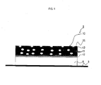
- FIG. 1 is a schematic cross sectional view illustrating a configuration of an electronic circuit 1 which the present invention is applied to.
- the electronic circuit 1 of the embodiment has a known configuration in which an electronic component 5, such as IC tip, is mounted on a surface of a printed circuit board 3 serving as an example of a circuit board.
- a heat sink 10 as described below is stacked on a surface of the electronic component 5.
- the heat sink 10 includes a porous ceramics 13 being 0-1-5.0 mm in thickness and having multiple pores 11. At a surface of the porous ceramics 13, a heat-releasing paint 15 having thermal emittance of 0.9 or more is applied on an entire circumferential surface as indicated by a black line in FIG. 1 . Further, a heat conducting tape 17 (one example of heat conducting sheet) is adhesively attached to one surface of the porous ceramics 13 (surface at the side stacked on the electronic component 5) while covering the heat-releasing paint 15.
- a heat conducting tape 17 one example of heat conducting sheet
- the porous ceramics 13 can be produced as described below for example. That is, it is able to be produced by weighing PVA, water, and ceramic raw materials described below, kneading by a kneader and granulating, forming by a mold, and sintering at a low temperature being 1200 °C or more and below 1400 °C (preferably 1300 °C or more and below 1400 °C) in the air.
- the composition of the ceramic raw materials can be formed, for example, by adding 1 part by weight of iron oxide into an entire raw material which is 100 parts by weight with 60-85 weight% of silicon carbide having an average particle diameter of 150 ⁇ m, 10-30 weight% of silica dioxide, and 1-10 weight% of alumina.
- the porous ceramics 13 having a volume resistivity of 10 10 Ohmxcm or more, a density of 1.6-3 g/cm 3 , and a porosity of 15-50 vol%.
- the heat-releasing paint 15 a commercial item, such as "CT-100" (product name: manufactured by okitsumo), can be used. Applying the heat-releasing paint 15 about 100 ⁇ m thickness ( ⁇ 10%) is preferable in order to ensure heat releasing characteristics of the heat sink 10 and to prevent ceramic powder from falling off. Still further, as the heat conducting tape 17, it is possible to use a tape made by filling alumina in an acryl adhesive material.
- the silicon carbide on the surface is converted to silica dioxide and the surface of the heat sink becomes roughened.
- the silica dioxide has thermal emittance higher than the one of the silicon carbide, and the roughness increases a surface area of the porous ceramics 13. Therefore, it is possible to further improve the heat releasing characteristics of the heat sink 10.
- the pores 11 are exposed also on an upper surface of the porous ceramics 13 (opposite side to the electronic component 5), and the heat-releasing paint 15 is applied on the entire circumferential surface, the heat releasing characteristics of the heat sink 10 is further improved.
- the heat sink 10 is configured with the porous ceramics 13 having a volume resistivity of 10 10 Ohm ⁇ cm or more which is a level of volume resistivity to be defined as an insulator in general. Therefore, it is possible to eliminate the occurrence of high frequency noise without an approach to be connected to an earth electrode.
- the porous ceramics 13 configuring the heat sink 10 has a porosity of 15-50 vol%. Therefore, it is lightweight with a density of 1.6-3.0 g/cm 3 and excels in workability when being processed into a given shape. Therefore, in the electronic circuit 1, freedom of designing is widely improved. Further, the heat sink 10 is 0.1-5.0 mm in thickness and is lightweight as described above, so that it is successfully applicable to an electronic circuit of an electronic device required to be smaller and lighter.
- the porous ceramics 13 does not use fine silicon carbide, which is less than 10 ⁇ m and is costly, used to obtain a dense sintered body. Further, the producing method is easy as described above. Therefore, it is possible to reduce the manufacturing cost. Further, the porous ceramics 13 manufactured as described above has a low thermal expansion coefficient, which is a linear expansion coefficient of about 3-5 ppm that is close to the one of a ceramic substrate. Therefore, it does not provide stress in vain to the electronic component 5.
- the heat-releasing paint 15 does not have to be applied at all, may be applied only to the upper surface of the porous ceramics 13, or may be applied to the entire surface excluding a bottom surface of the porous ceramics 13.
- This type of heat sink 10 sometimes may be stacked on the electronic component 5 via a liquid substance having thermal conductivity, such as thermal conductive grease or thermal conductive adhesive.
- thermal conductivity such as thermal conductive grease or thermal conductive adhesive.
- the heat sink 10 is configured with the porous ceramics 13 as described above, it is possible to maintain the liquid substance in the pores. Accordingly, in this case, it is possible to inhibit the liquid substance dripping.
- the heat sink 10 is stacked on the electronic component 5 interposing a commercial heat conducting sheet such as "COOL PROVEIDE (product name: manufactured by Kitagawa Industries Co., Ltd.)" for example.
- COOL PROVEIDE product name: manufactured by Kitagawa Industries Co., Ltd.
- the heat conducting tape 17 by directly sticking the heat sink 10 onto the electronic component 5 via the heat conducting tap 17, it can be configured easily such that the heat sink 10 is stacked on the electronic component 5 with the heat conducting tape 17, as one example of a heat conducting sheet, interposed therebetween.
- Porosity it was measured by use of a testing machine (product name: AutoPore IV 9500, manufactured by Micromeritics).
- Volume resistivity it was measured by a testing machine (product name: Hiresta, manufactured by Mitsubishi Chemical). When the value was less than 1 ⁇ 10 10 Ohm-centimeter (Ohm ⁇ cm), it was evaluated “x”. When the value was within 1 ⁇ 10 10 Ohm-centimeter (Ohmxcm) to 2 ⁇ 10 10 Ohm-centimeter (Ohm ⁇ cm), it was evaluated “ ⁇ ”. When the value was 2 ⁇ 10 10 Ohm-centimeter (Ohmxcm) or more, it was evaluated " ⁇ ".
- Heat-releasing characteristics a heat source was set to have a surface temperature at 90 °C, the specimen was mounted on its surface, and the surface temperature of the heat source stabilized in thirty minutes after being left was measured by use of a K-type thermocouple.
- 20.9 °C drop 69.1 °C being a value of an aluminum plate (20 x 20 x 3 mm) of which heat-releasing characteristics was measured under the same condition
- when the reduction in temperature was less than 20 °C it was evaluated "x”.
- the reduction in temperature was within 20-20.9 °C, it was evaluated " ⁇ ”.
- the reduction in temperature was 20.9 °C or more, it was evaluated " ⁇ ".
- the overall evaluation was made considering all of the above evaluations together. Specifically, when all the evaluations were " ⁇ ”, it was overall evaluated “ ⁇ ”. When there was at least one " ⁇ ”, it was overall evaluated “ ⁇ ”. When there was at least one "x”, it was overall evaluated "x”.
- the volume resistivity was 1x10 10 Ohm-centimeter (Ohmxcm) or more and that heat-releasing characteristics was able to be ensured to be equal to or greater than the one of aluminum (overall evaluation " ⁇ , ⁇ ").
- Example 2 Example 3, and Example 4
- the volume resistivities were 2x10 10 Ohm-centimeter (Ohmxcm), 21.5x10 10 Ohm-centimeter (Ohmxcm), and 50x10 10 Ohm-centimeter (Ohmxcm), respectively.
Landscapes
- Engineering & Computer Science (AREA)
- Mechanical Engineering (AREA)
- General Engineering & Computer Science (AREA)
- Physics & Mathematics (AREA)
- Thermal Sciences (AREA)
- Ceramic Engineering (AREA)
- Dispersion Chemistry (AREA)
- Chemical & Material Sciences (AREA)
- Microelectronics & Electronic Packaging (AREA)
- Cooling Or The Like Of Semiconductors Or Solid State Devices (AREA)
- Porous Artificial Stone Or Porous Ceramic Products (AREA)
- Compositions Of Oxide Ceramics (AREA)
- Cooling Or The Like Of Electrical Apparatus (AREA)
Abstract
Description
- This international application claims the benefits of Japanese Patent Application No.
2010-253005 filed November 11, 2010 2011-246722 filed November 10, 2011 2010-253005 2011-246722 - The present invention relates to an electronic circuit, which is provided with a circuit board on which an electronic component is mounted, a heat conducting sheet stacked on the electronic component, and a heat sink stacked on the heat conducting sheet. The present invention further relates to a heat sink available for the electronic circuit.
- In an electronic circuit having an electronic component, such as IC, mounted on a circuit board, it has been an object to release efficiently heat which the electronic component generates. It has been thus proposed to stack a heat sink on a surface of the electronic component mounted on the circuit board via a heat conducting sheet having high thermal conductivity. Accordingly, it is possible to release the heat generated by the electronic component to the side of the heat sink via the heat conducting sheet, thereby enabling to release the heat from the heat sink.
- As this type of heat sink, some metallic heat sink has been commonly used, which is given with microfabrication by die-casting or machine processing and then of which surface area is increased. Meanwhile, some heat sink has been proposed, which is produced by casting metallic molten metal into a porous ceramics obtained by sintering silicon carbide (e.g., see Patent Document 1).
-
- Patent Document 1: Japanese Patent No.
4233133 - However, because any of the above heat sinks are conductors, when the heat sink is stacked on the surfaces of the electronic component with the heat conducting sheet interposed therebetween, it would be configured so that two conductors are arranged in parallel, with the interposing heat conducting sheet being an insulator. According to this configuration, high frequency noise was likely to be generated. Therefore, so as not to generate this high frequency noise, an approach, for example, has been considered to connect the heat sink to an earth electrode of the circuit board. In this case, limitation on designing of the electronic circuit occurs.
- In light of the forgoing, the present invention has been made for the purpose of providing an electronic circuit having an improved freedom of designing by use of a heat sink made of an insulator and for the purpose of providing an insulating heat sink available for the electronic circuit.
- An electronic circuit of the present invention made in order to achieve the above object includes a circuit board on which an electronic component is mounted, a heat conducting sheet stacked on the electronic component, and a heat sink stacked on the heat conducting sheet, and in that the heat sink includes a porous ceramics having a volume resistivity of 1010 Ohm×cm or more and a porosity of 15-50 vol%.
- In the electronic circuit of the present invention configured as described above, it is possible to let heat generated by the electronic component go to the side of the heat sink via the heat conducting sheet and to release the heat from the heat sink.
- Further, the heat sink is made of the porous ceramics having a volume resistivity of 1010 Ohmxcm or more, which is a level of volume resistivity to be generally defined as an insulator. Therefore, it is possible to inhibit high frequency noise from occurring without an approach to connect the heat sink to an earth electrode as described above.
- In addition, since the porous ceramics configuring the heat sink has the porosity of 15-50 vol%, it is lightweight, excels in heat releasing, and excels in workability when it is formed into a given shape. Therefore, in the electronic circuit of the present invention, freedom of designing is improved widely.
- The heat sink of the present invention includes the porous ceramics having a volume resistivity of 1010 Ohmxcm or more and a porosity of 15-50 vol%. The heat sink of the present invention configured as described above includes the porous ceramics having a volume resistivity of 1010 Ohmxcm or more, which is a level of volume resistivity to be generally defined as an insulator.
- Therefore, when the heat sink is stacked on the electronic component via the heat conducting sheet, it is possible to inhibit high frequency noise from occurring without an approach to connect the heat sink to an earth electrode as described above.
- In addition, since the porous ceramics configuring the heat sink has the porosity of 15-50 vol%, it is lightweight, excels in heat releasing, and excels in workability when it is formed into a given shape.
- As material for the porous ceramics having a volume resistivity of 1010 Ohm×cm or more, which is a level of volume resistivity to be generally defined as an insulator, alumina (AlzO3), silica (silica dioxide: SiO2), zirconia (ZrO2), etc. are listed.
- The porosity of the porous ceramics of the present invention can be set to a target porosity by mixing a volatile element, which volatiles and disappears when baking, to the above mentioned alumina, silica, etc. It is set by mixing the volatile element, such as PVA for example, by the degree of a target porosity and by baking after molding into a given shape of the heat sink. Besides this, a method of making some conventional ceramics porous is available.
- When the porosity of the porous ceramics is 15 vol% or more, insulation properties are good and volume resistivity can be secured.
- Meanwhile, when it is 50 vol% or less, air having high thermal insulation properties becomes less inside the porous ceramics. Therefore, heat releasing is good.
- The density of the porous ceramics may be 1.6-3 g/cm3. In this case, the heat sink has remarkably good lightweight properties and can be applied preferably to an electronic circuit of an electronic device required to be smaller and lighter.
- The porous ceramics may be made by sintering granulated particles obtained by mixing at least silica dioxide, alumina, and silicon carbide (SiC). Here, a particle diameter of each particle of the granulated particles may be 10 µm.
- A large particle having a particle diameter of 10 µm or more is usually used as a polishing agent and is unfavorable as a material for ceramics because a sintered body obtained is not densified. However, an applicant of the present invention has found that it is possible to easily manufacture the above described porous ceramics by sintering the granulated particles, each particle having a particle diameter of 10 µm or more, obtained by mixing at least silica dioxide, alumina, and silicon carbide.
- Accordingly, when the above described porous ceramics is made by sintering the granulated particles, each particle having a particle diameter of 10 µm or more, obtained by mixing at least silica dioxide, alumina, and silicon carbide, it is possible to reduce preferably manufacturing (material) costs of the heat sink.
- Further, it is preferable to set an upper limit of the particle diameter of the granulated particle at 1250 µm. Granulated particles having any greater particle diameters than this one have difficulty in being manufactured and is likely to crumble after being molded in to a predetermined shape and to have difficulty in remaining in the same shape. Therefore, the particle diameter of the granulated particle is preferably in the range of 10-1250 µm.
- Further, it is preferable that the average particle diameter of the silicon carbide is 10 µm or more and 150 µm or less.
- When the average particle diameter is 150 µm or less, following advantages are given. That is: (1) It is possible to enhance insulation properties of the heat sink configured with the porous ceramics obtained therefrom. That is, the volume resistivity is further increased, so that a value of 1010 Ohm-centimeter (Ohm×cm) or more can be achieved easily. This is because, when the average particle diameter of the silicon carbide exceeds 150 µm, respective particles of the silicon carbide are drawn near one another in the matrix of the porous ceramics. Separate intervals therebetween are hence shortened, so that electric conduction becomes easier via the silicon carbide. (2) The granulated particles can be granulated easily, in other words in a short amount of time. This is because, when the silicon carbide being one of the particles configuring the granulated particles is fine, the silicon carbide can disperse uniformly inside the granulated particles. As described above, from the granulated particles configured with materials each dispersed uniformly, a porous ceramics, i.e., heat sink, having a stabilized physical property can be obtained.
- Meanwhile, when the average particle diameter of the silicon carbide is 10 µm or more, a procurement of the material is allowed at a low price (because the particle of the silicon carbide is large, for example, such as that kind of silicon carbide used as a polishing agent), thereby enabling to reduce the manufacturing (material) costs easily.
- Still further, also regarding the silica dioxide and the alumina, it is preferable that the average particle diameter of each is 1 µm or more. When the particle diameter is 1 µm or more, a procurement of the material is allowed at a low cost, thereby enabling to reduce the manufacturing (material) cost easily.
- Meanwhile, the upper limits of the average particle diameters of the silica dioxide and the alumina are not limited specifically as far as the particle diameter of the granulated particle obtained therefrom becomes 10-1250 µm. However, in general, it is preferable that the average particle diameter is less than 10 µm. It is because the granulated particles can be granulated easily, i.e., in a short amount of time.
- The granulated particles are manufactured by mixing the above materials for ceramics and binder by use of a mixer, kneader for example.
- Regarding the heat sink of the present invention, the porous ceramics may be made by sintering granulated particles obtained by mixing 60-85 weight% of silicon carbide and at least 10 weight% or more of silica dioxide. In this case, it is possible to manufacture further stably and easily the porous ceramics having the above described volume resistivity and porosity.
- Further, it is needless to say that material, such as water, iron oxide, used to sinter a generally used ceramics may be added supplementarily in addition to the above composition.
- Specifically, when the silicon carbide is 60 weight% or more, further sufficient heat releasing characteristics can be obtained. This attributes to that, since the silicon carbide having a good thermal conductivity is rich in the matrix, it is possible to sufficiently ensure a heat conduction path and that, since the amounts of silica dioxide and alumina are reduced relatively, the porosity is increased and convective effect of the heat is lowered.
- Meanwhile, when the silicon carbide is 85 weight% or less, relative permittivity is lowered, thereby enabling to ensure higher insulation properties.
- When the silica dioxide is 10 weight% or more, the strength of the heat sink is increased. Therefore, even if the heat sink is shaped so that it becomes brittle having multiple protrusions for example, it is possible to ensure a sufficient strength as a heat sink.
- Meanwhile, when the silica dioxide is 40 weight% or less, heat releasing characteristics is further improved. This is because, when the amount of silica dioxide is 40 weight% or less, the silica dioxide is bound with silicon carbide more strongly when baking the porous ceramics, the diameter of each pore hence becomes less, and heat transferring by air convention in each pore becomes worse. This means that a porous ceramics having a less amount of silica dioxide shows higher heat releasing characteristics even if the porosities are the same.
- Further, granulated particles may be obtained by mixing at least 1 weight% or more of alumina with the above-described silicon carbide and silica dioxide.
- When this alumina is 1 weight% or more, the strength of the heat sink is further increased. Therefore, even when the heat sink is shaped such that it becomes brittle having multiple protrusions for example, it is possible to ensure a sufficient strength as a heat sink. That is, the heat sink of the present invention may be shaped to have such protrusions, and "stacking" of the present invention may be an arrangement of at least overlapping.
- Meanwhile, when the alumina exceeds 10 weight%, it should be noted that there is a possibility that a problem of lowering of heat releasing characteristics becomes obvious, which is due to the diminishing of the pore diameter as described above.
- Besides the above, it is preferable that the above described sintering is performed at the oxygen ambient (for example, in the air). In this case, regarding the silicon carbide exposed to the surface, as a result of oxidation, its carbon element is desorbed as carbon dioxide and its silicon element is formed to silica dioxide.
- Here, (1) it has been known that silica dioxide has thermal emittance higher than the one of silicon carbide. Further, (2) at the surface of the silicon carbide, a surface area per unit weight is increased by roughness caused by decarburization.
- The above descried effects (1) and (2) further enhances the heat releasing characteristics of the heat sink. Therefore, when it is applied to the electronic circuit as described above, it is possible to further favorably inhibit an electronic component from overheating.
- According to the heat sink of the present invention, a heat-releasing paint having a thermal emittance of 0.9 or more may be applied on its surface. In this case, it is possible to further improve heat releasing characteristics of the heat sink and furthermore possible to further favorably inhibit an electronic component from overheating when it is applied to the electronic circuit as described above. The above 0.9 is a value arbitrarily set as a value higher than a thermal emittance of silicon carbide in consideration of that the thermal emittance of silicon carbide is 0.7.
- In addition, in this case, the heat-releasing paint may be applied to the entire circumferential surface of the heat sink and a heat conducting tape may be adhesively attached to one surface of the heat sink. In this case, the heat sink can be directly attached to the electronic component via the heat conducting tape. Accordingly, it can be configured easily such that the heat sink is stacked on the electronic component with the heat conducting tape, as an example of the heat conducting sheet, interposed therebetween.
- According to the heat sink of the present invention, the porous ceramics may possess some liquid substance having thermal conductivity in the pores. This type of heat sink is sometimes stacked on the electronic component via some liquid substance, such as thermal conductive grease, thermal conductive adhesive, having thermal conductivity. Since the heat sink of the present invention is configured with the porous ceramics as described above, it is possible to retain the liquid substance in the pores. Accordingly, in this case, it is possible to inhibit the liquid substance from dripping.
- The heat sink of the present invention may be 0.1-5.0 mm in thickness. In this case, the heat sink becomes light and easy to use, and can be applied further favorably to an electronic circuit for an electronic device required to be smaller and lighter.
-
-
FIG. 1 is a schematic cross sectional view illustrating a configuration of an electronic circuit to which the present invention is applied. -
- 1
- electronic circuit,
- 3
- printed circuit board,
- 5
- electronic component,
- 10
- heat sink,
- 11
- pores,
- 13
- porous ceramics,
- 15
- heat-releasing paint,
- 17
- heat conducting tape
- Next, an embodiment of the present invention will be described with reference to the drawing.
FIG. 1 is a schematic cross sectional view illustrating a configuration of an electronic circuit 1 which the present invention is applied to. As illustrated inFIG. 1 , the electronic circuit 1 of the embodiment has a known configuration in which an electronic component 5, such as IC tip, is mounted on a surface of a printed circuit board 3 serving as an example of a circuit board. Aheat sink 10 as described below is stacked on a surface of the electronic component 5. - The
heat sink 10 includes aporous ceramics 13 being 0-1-5.0 mm in thickness and havingmultiple pores 11. At a surface of theporous ceramics 13, a heat-releasingpaint 15 having thermal emittance of 0.9 or more is applied on an entire circumferential surface as indicated by a black line inFIG. 1 . Further, a heat conducting tape 17 (one example of heat conducting sheet) is adhesively attached to one surface of the porous ceramics 13 (surface at the side stacked on the electronic component 5) while covering the heat-releasingpaint 15. - Here, the
porous ceramics 13 can be produced as described below for example. That is, it is able to be produced by weighing PVA, water, and ceramic raw materials described below, kneading by a kneader and granulating, forming by a mold, and sintering at a low temperature being 1200 °C or more and below 1400 °C (preferably 1300 °C or more and below 1400 °C) in the air. - The composition of the ceramic raw materials can be formed, for example, by adding 1 part by weight of iron oxide into an entire raw material which is 100 parts by weight with 60-85 weight% of silicon carbide having an average particle diameter of 150 µm, 10-30 weight% of silica dioxide, and 1-10 weight% of alumina. By such method of producing, it is possible to obtain preferably the
porous ceramics 13 having a volume resistivity of 1010 Ohmxcm or more, a density of 1.6-3 g/cm3, and a porosity of 15-50 vol%. - Further, as the heat-releasing
paint 15, a commercial item, such as "CT-100" (product name: manufactured by okitsumo), can be used. Applying the heat-releasingpaint 15 about 100 µm thickness (±10%) is preferable in order to ensure heat releasing characteristics of theheat sink 10 and to prevent ceramic powder from falling off. Still further, as theheat conducting tape 17, it is possible to use a tape made by filling alumina in an acryl adhesive material. - In the
porous ceramics 13 produced as described above, at a time of sintering, the silicon carbide on the surface is converted to silica dioxide and the surface of the heat sink becomes roughened. The silica dioxide has thermal emittance higher than the one of the silicon carbide, and the roughness increases a surface area of theporous ceramics 13. Therefore, it is possible to further improve the heat releasing characteristics of theheat sink 10. In addition, as illustrated inFIG. 1 , since thepores 11 are exposed also on an upper surface of the porous ceramics 13 (opposite side to the electronic component 5), and the heat-releasingpaint 15 is applied on the entire circumferential surface, the heat releasing characteristics of theheat sink 10 is further improved. - Therefore, in the electronic circuit 1 in which the
heat sink 10 described above is stacked on the electronic component 5 with theheat conducting tape 17 interposed therebetween, it is possible to let heat generated by the electronic component 5 go to the side of theheat sink 10 via theheat conducing tape 17 and to release successfully the heat from theheat sink 10. In addition, theheat sink 10 is configured with theporous ceramics 13 having a volume resistivity of 1010 Ohm×cm or more which is a level of volume resistivity to be defined as an insulator in general. Therefore, it is possible to eliminate the occurrence of high frequency noise without an approach to be connected to an earth electrode. - Further, the
porous ceramics 13 configuring theheat sink 10 has a porosity of 15-50 vol%. Therefore, it is lightweight with a density of 1.6-3.0 g/cm3 and excels in workability when being processed into a given shape. Therefore, in the electronic circuit 1, freedom of designing is widely improved. Further, theheat sink 10 is 0.1-5.0 mm in thickness and is lightweight as described above, so that it is successfully applicable to an electronic circuit of an electronic device required to be smaller and lighter. - Still further, the
porous ceramics 13 does not use fine silicon carbide, which is less than 10 µm and is costly, used to obtain a dense sintered body. Further, the producing method is easy as described above. Therefore, it is possible to reduce the manufacturing cost. Further, theporous ceramics 13 manufactured as described above has a low thermal expansion coefficient, which is a linear expansion coefficient of about 3-5 ppm that is close to the one of a ceramic substrate. Therefore, it does not provide stress in vain to the electronic component 5. - The present invention should not be construed as limited to the embodiment set forth above and can be achieved in any modes within the scope of the present invention. For example, the heat-releasing
paint 15 does not have to be applied at all, may be applied only to the upper surface of theporous ceramics 13, or may be applied to the entire surface excluding a bottom surface of theporous ceramics 13. This type ofheat sink 10 sometimes may be stacked on the electronic component 5 via a liquid substance having thermal conductivity, such as thermal conductive grease or thermal conductive adhesive. In this case, since theheat sink 10 is configured with theporous ceramics 13 as described above, it is possible to maintain the liquid substance in the pores. Accordingly, in this case, it is possible to inhibit the liquid substance dripping. In addition, when inhibitory effect of such dripping is expected, it may be sometimes preferable not to apply the heat-releasingpaint 15 or apply excluding the bottom surface. - Further, it is possible to omit the
heat conducting tape 17. In this case, theheat sink 10 is stacked on the electronic component 5 interposing a commercial heat conducting sheet such as "COOL PROVEIDE (product name: manufactured by Kitagawa Industries Co., Ltd.)" for example. However, as described above, when theheat conducting tape 17 is provided, by directly sticking theheat sink 10 onto the electronic component 5 via theheat conducting tap 17, it can be configured easily such that theheat sink 10 is stacked on the electronic component 5 with theheat conducting tape 17, as one example of a heat conducting sheet, interposed therebetween. - Experimental examples concerning the heat sink of the present invention will be explained below in detail.
- 1. The granulated particles are manufactured by mixing the ceramic raw materials blended in accordance with the blend ratio (weight%) indicated at the right column of Table 1 with the other component (1 parts by weight or less of iron oxide out of 100 parts by weight of ceramic raw materials) at a required amount and binder, whereby each of the granulated particles is sized to a required particle diameter. The mixed quantity of the binder is determined in a manner that a specimen (heat sink) obtains a certain level of porosity.
- 2. A plate-like body is molded from the granulated particles, which is then formed to be a plate-like specimen (heat sink) of 20 x 20 x 3 mm after baking.
- 3. The specimen is obtained by baking the plate-like body under the condition of 1350 °C at an ambient environment.
- 4. The handling (moldability) of the plate-like body and the porosity, volume resistivity, and heat-releasing characteristics, of the specimen obtained were measured and evaluated by the method described below.
- Handling (moldability): If, at the time of molding the plate-like body at the step of the above 2, the plate-like body was moldable, was able to be thrown to a baking furnace, and the baking was completed while maintaining the shape of the plate-like body, it was evaluated "o". If the plate-like body was not able to be molded (e.g., crumbling), or if the plate-like body was molded but was not able to be thrown to the baking furnace and the baking was not completed, it was evaluated "x".
- Porosity: it was measured by use of a testing machine (product name: AutoPore IV 9500, manufactured by Micromeritics).
- Volume resistivity: it was measured by a testing machine (product name: Hiresta, manufactured by Mitsubishi Chemical). When the value was less than 1×10¹⁰ Ohm-centimeter (Ohm×cm), it was evaluated "x". When the value was within 1×10¹⁰ Ohm-centimeter (Ohmxcm) to 2×10¹⁰ Ohm-centimeter (Ohm×cm), it was evaluated "Δ". When the value was 2×10¹⁰ Ohm-centimeter (Ohmxcm) or more, it was evaluated "○".
- Heat-releasing characteristics: a heat source was set to have a surface temperature at 90 °C, the specimen was mounted on its surface, and the surface temperature of the heat source stabilized in thirty minutes after being left was measured by use of a K-type thermocouple. With reference to 20.9 °C drop (69.1 °C) being a value of an aluminum plate (20 x 20 x 3 mm) of which heat-releasing characteristics was measured under the same condition, when the reduction in temperature was less than 20 °C, it was evaluated "x". When the reduction in temperature was within 20-20.9 °C, it was evaluated "Δ". When the reduction in temperature was 20.9 °C or more, it was evaluated "○".
- The overall evaluation was made considering all of the above evaluations together. Specifically, when all the evaluations were "○", it was overall evaluated "⊚". When there was at least one "Δ", it was overall evaluated "○". When there was at least one "x", it was overall evaluated "x".
- Materials employed were as follows respectively.
- SiC: product name: GP1000, manufactured by Shinano Electric Refining Co., Ltd. (average particle diameter 12 µm)
- SiC: product name: GP400, manufactured by Shinano Electric Refining Co., Ltd. (average particle diameter 35 µm)
- SiC: product name: GC100, manufactured by Shinano Electric Refining Co., Ltd. (average particle diameter 150 µm)
- SiC: product name: GC80, manufactured by Shinano Electric Refining Co., Ltd. (average particle diameter 180 µm)
- SiO2: product name: silicon oxide(IV), powder, 1.0 micron, 99.9%, manufactured by Wako Pure Chemical Industries, Ltd. (average particle diameter 1 µm)
- AlaO3: product name: AL-43-L, manufactured by Showa Denko K.K. (average particle diameter 1 µm)
- iron oxide (Fe2O3): product name: iron oxide (III), manufactured by Wako Pure Chemical Industries, Ltd. (average particle diameter 1 µm)
- binder: PVA (product name: JP-05, manufactured by Japan Vam & Poval Co., Ltd.)
- Regarding the porosity of the specimen obtained, as indicated in Table 1, within the range of 15-50 vol%, it was confirmed that the volume resistivity was 1x10¹⁰ Ohm-centimeter (Ohmxcm) or more and that heat-releasing characteristics was able to be ensured to be equal to or greater than the one of aluminum (overall evaluation "⊚, ○").
- When the porosity was less than 15 vol%, it was not possible to ensure the volume resistivity of 1x10¹⁰ Ohm-centimeter (Ohmxcm) (comparative example 1). when this porosity exceeded 50 vol%, it was not possible to ensure heat-releasing characteristics (comparative example 2).
- When the blend ratio of the silicon carbide was in the range of 60-85 weight%, it was confirmed that the high heat-releasing characteristics and the volume resistivity of 1x10¹⁰ Ohm×cm or more was ensured regardless the average particle diameter of the silicon carbide.
- When the blend ratio of the silicon carbide was less than 60 weight%, it was not possible to ensure heat-releasing characteristics (comparative example 5). When the blend ratio exceeded 85 weight%, it was not possible to ensure the volume resistivity of 1x10¹⁰ Ohm-centimeter (Ohmxcm) (comparative example 6).
- Further, regarding Example 2, Example 3, and Example 4, the volume resistivities were 2x10¹⁰ Ohm-centimeter (Ohmxcm), 21.5x10¹⁰ Ohm-centimeter (Ohmxcm), and 50x1010 Ohm-centimeter (Ohmxcm), respectively. The reduction in temperature, which denotes the heat-releasing characteristics of Example 3, was 23.4 °C.
- Regarding the granulated particles, when its particle diameter was 1250 µm or less, it was confirmed to be able to ensure moldability and to be able to manufacture optimally a heat sink of the present invention. Meanwhile, when its particle exceeds 1250 µm (comparative example 3), it was not possible to ensure moldability.
| Experimental Example | SiC(µm) | Al2O3 | SiO3 | Granulated Particle (µm) | Porosity (vol%) | Moldability | Volume Resistivity | Host Releasing Characteristics | Overall Evaluation | |||
| 12 | 36 | 150 | 180 | |||||||||
| Example 1 | 30 | 30 | 10 | 30 | 100∼500 | 15 | ○ | Δ | ○ | ○ | ||
| Example 2 | ↑ | ↑ | ↑ | ↑ | ↑ | 35 | ○ | ○ (2×10¹⁰Ω·cm) | ○ | ⊚ | ||
| Example 3 | ↑ | ↑ | ↑ | ↑ | ↑ | 45 | ○ | ○ (21.5×10¹⁰Ω·cm) | ○ (23.4°C) | ⊚ | ||
| Example 4 | ↑ | ↑ | ↑ | ↑ | ↑ | 50 | ○ | ○ (50×1010Ω·cm) | Δ | ○ | ||
| Example 5 | 30 | 35 | 5 | 30 | ↑ | 15 | ○ | Δ | ○ | ○ | ||
| Example 6 | ↑ | ↑ | ↑ | ↑ | ↑ | 50 | ○ | ○ | Δ | ○ | ||
| Comparative Example 1 | 35 | 40 | 5 | 20 | ↑ | 10 | ○ | × | ○ | × | ||
| Example 7 | ↑ | ↑ | ↑ | ↑ | ↑ | 15 | ○ | Δ | ○ | ○ | ||
| Example 8 | ↑ | ↑ | ↑ | ↑ | ↑ | 35 | ○ | ○ | ○ | ⊚ | ||
| Example 9 | ↑ | ↑ | ↑ | ↑ | ↑ | 50 | ○ | ○ | Δ | ○ | ||
| Comparative Example 2 | ↑ | ↑ | ↑ | ↑ | ↑ | 55 | ○ | ○ | × | × | ||
| Comparative Example 3 | ↑ | ↑ | ↑ | ↑ | 1300∼1500 | 35 | × | not moldable so not measured | × | |||
| Example 10 | ↑ | ↑ | ↑ | ↑ | 500∼1250 | ↑ | ○ | ○ | ○ | ⊚ | ||
| Example 11 | ↑ | ↑ | 25 | 100∼500 | 35 | ○ | ○ | ○ | ⊚ | |||
| Example 12 | 75 | 5 | 20 | ↑ | 35 | ○ | ○ | ○ | ⊚ | |||
| Example 13 | 75 | ↑ | ↑ | ↑ | ↑ | ○ | ○ | ○ | ⊚ | |||
| Example 14 | 75 | ↑ | ↑ | ↑ | 15 | ○ | ○ | ○ | ⊚ | |||
| Example 15 | ↑ | ↑ | ↑ | ↑ | 35 | ○ | Δ | ○ | ○ | |||
| Example 16 | 75 | ↑ | ↑ | ↑ | 15 | ○ | Δ | ○ | ○ | |||
| Comparative Example 4 | ↑ | ↑ | ↑ | ↑ | 35 | ○ | × | ○ | × | |||
| Example 17 | 25 | 25 | 25 | ↑ | ↑ | ↑ | ↑ | ○ | ○ | ○ | ○ | |
| Example 18 | 40 | 45 | 5 | 10 | ↑ | 15 | ○ | Δ | ○ | ○ | ||
| Example 19 | ↑ | ↑ | ↑ | ↑ | ↑ | 35 | ○ | ○ | ○ | ⊚ | ||
| Example 20 | ↑ | ↑ | ↑ | ↑ | ↑ | 50 | ○ | ○ | Δ | ○ | ||
| Example 21 | 45 | 40 | ↑ | ↑ | ↑ | 15 | ○ | Δ | ○ | ○ | ||
| Example 22 | ↑ | ↑ | ↑ | ↑ | ↑ | 35 | ○ | ○ | ○ | ⊚ | ||
| Example 23 | ↑ | ↑ | ↑ | ↑ | ↑ | 50 | ○ | ○ | Δ | ○ | ||
| Comparative Example 5 | 25 | 30 | 15 | 30 | ↑ | 35 | ○ | ○ | × | × | ||
| Comparative Example 6 | 40 | 50 | ↑ | 9 | ↑ | ↑ | ○ | × | ○ | × | ||
Claims (5)
- An electronic circuit comprising: a circuit board on which an electronic component is mounted; a heat conducting sheet stacked on the electronic component; and a heat sink stacked on the heat conducting sheet, wherein the heat sink comprises a porous ceramics having a volume resistivity of 1010 Ohmxcm or more and a porosity of 15-50 vol%.
- A heat sink characterized in comprising a porous ceramics having a volume resistivity of 1010 Ohmxcm or more and a porosity of 15-50 vol%.
- The heat sink according to claim 2, wherein the porous ceramics is made by sintering granulated particles obtained by mixing at least silica dioxide, alumina, and silicon carbide, and each particle of the granulated particles has a particle diameter of 10 µm or more.
- The heat sink according to claim 3, wherein the silicon carbide has an average particle diameter of 150 µm or less.
- The heat sink according to any one of claims 2-4, wherein the porous ceramics is made by sintering granulated particles obtained by mixing 60-85 weight% of silicon carbide and at least 10 weight% or more of silica dioxide.
Applications Claiming Priority (3)
| Application Number | Priority Date | Filing Date | Title |
|---|---|---|---|
| JP2010253005 | 2010-11-11 | ||
| JP2011246722A JP2012119671A (en) | 2010-11-11 | 2011-11-10 | Electronic circuit and heat sink |
| PCT/JP2011/076099 WO2012063942A1 (en) | 2010-11-11 | 2011-11-11 | Electronic circuit and heat sink |
Publications (3)
| Publication Number | Publication Date |
|---|---|
| EP2639827A1 true EP2639827A1 (en) | 2013-09-18 |
| EP2639827A4 EP2639827A4 (en) | 2017-12-27 |
| EP2639827B1 EP2639827B1 (en) | 2020-12-09 |
Family
ID=46051079
Family Applications (1)
| Application Number | Title | Priority Date | Filing Date |
|---|---|---|---|
| EP11840114.0A Active EP2639827B1 (en) | 2010-11-11 | 2011-11-11 | Method for manufacturing an electronic circuit comprising a heat sink |
Country Status (5)
| Country | Link |
|---|---|
| US (2) | US20130220676A1 (en) |
| EP (1) | EP2639827B1 (en) |
| JP (1) | JP2012119671A (en) |
| CN (1) | CN103222046B (en) |
| WO (1) | WO2012063942A1 (en) |
Families Citing this family (5)
| Publication number | Priority date | Publication date | Assignee | Title |
|---|---|---|---|---|
| CN104752375A (en) * | 2013-12-27 | 2015-07-01 | 奇鋐科技股份有限公司 | Semiconductor cooling structure |
| US10568205B2 (en) | 2016-07-27 | 2020-02-18 | Corning Incorporated | Ceramic and polymer composite, and uses thereof |
| CN207869432U (en) * | 2018-03-07 | 2018-09-14 | 东莞市国研电热材料有限公司 | A multi-temperature zone ceramic heating element |
| WO2020145365A1 (en) * | 2019-01-10 | 2020-07-16 | 日本碍子株式会社 | Heat dissipation member |
| CN117203176A (en) | 2021-04-21 | 2023-12-08 | 三菱电机株式会社 | Cooling components and radiators |
Family Cites Families (30)
| Publication number | Priority date | Publication date | Assignee | Title |
|---|---|---|---|---|
| CA1043666A (en) * | 1973-01-08 | 1978-12-05 | Champion Spark Plug Company | Method for producing a semi-conductor body comprising silicon carbide, silica and alumina |
| JPS58101442A (en) * | 1981-12-11 | 1983-06-16 | Hitachi Ltd | Substrate for electric device |
| US5347426A (en) * | 1988-09-13 | 1994-09-13 | Pechiney Recherche | Electronic device including a passive electronic component |
| FR2639343B1 (en) * | 1988-11-21 | 1991-02-15 | Eyquem | SEMICONDUCTOR CERAMIC COMPOSITION AND ITS APPLICATION IN THE MANUFACTURE OF SPARK PLUGS |
| KR0177972B1 (en) * | 1990-12-17 | 1999-03-20 | 김정배 | Inner Sealed Clip |
| US5386143A (en) * | 1991-10-25 | 1995-01-31 | Digital Equipment Corporation | High performance substrate, electronic package and integrated circuit cooling process |
| JP3072189B2 (en) * | 1992-08-12 | 2000-07-31 | イビデン株式会社 | Heat dissipation board for semiconductor devices |
| JP3596910B2 (en) * | 1993-06-14 | 2004-12-02 | 新原 ▲晧▼一 | Porous ceramic body and method for producing the same |
| DE19529627C1 (en) * | 1995-08-11 | 1997-01-16 | Siemens Ag | Thermally conductive, electrically insulating connection and method for its production |
| JPH1129379A (en) * | 1997-02-14 | 1999-02-02 | Ngk Insulators Ltd | Composite material for semiconductor heat sink and method of manufacturing the same |
| JP4233133B2 (en) | 1997-10-21 | 2009-03-04 | 電気化学工業株式会社 | Silicon carbide composite and heat dissipation component using the same |
| JP3983362B2 (en) * | 1997-12-10 | 2007-09-26 | 日本碍子株式会社 | Porous composite ceramics and method for producing the same |
| JP3468358B2 (en) * | 1998-11-12 | 2003-11-17 | 電気化学工業株式会社 | Silicon carbide composite, method for producing the same, and heat radiation component using the same |
| KR20010079642A (en) * | 1999-06-14 | 2001-08-22 | 오카야마 노리오 | Composite Material and Semiconductor Device Using the Same |
| ES2341274T3 (en) * | 1999-09-29 | 2010-06-17 | Ibiden Co., Ltd. | PANAL FILTER AND CERAMIC FILTER ASSEMBLY. |
| JP4426083B2 (en) * | 2000-11-17 | 2010-03-03 | 日本碍子株式会社 | Silicon carbide based porous material and method for producing the same |
| CN1341578A (en) * | 2001-08-17 | 2002-03-27 | 中国科学院上海硅酸盐研究所 | Method for preparing silicon carbide porous ceramic pipe |
| US6705393B1 (en) * | 2003-02-25 | 2004-03-16 | Abc Taiwan Electronics Corp. | Ceramic heat sink with micro-pores structure |
| JP3100267U (en) * | 2003-09-04 | 2004-05-13 | 千如電機工業股▲ふん▼有限公司 | Porous ceramic radiator |
| JP2006261519A (en) | 2005-03-18 | 2006-09-28 | Sharp Corp | Semiconductor device and manufacturing method thereof |
| JP2007173338A (en) * | 2005-12-20 | 2007-07-05 | Mitsubishi Gas Chem Co Inc | High thermal conductive adhesive sheet and method of using the same |
| EP1973157B1 (en) * | 2006-01-13 | 2017-06-21 | Denka Company Limited | Aluminum/silicon carbide composite and heat dissipation device employing the same |
| JP2008010761A (en) * | 2006-06-30 | 2008-01-17 | Fanuc Ltd | Electronic component heat sink |
| WO2008008496A2 (en) * | 2006-07-14 | 2008-01-17 | Dow Global Technologies Inc. | Improved composite material and method of making the composite material |
| US20080203557A1 (en) * | 2007-01-30 | 2008-08-28 | Sanyo Electric Co., Ltd. | Semiconductor module and method of manufacturing the same |
| JP2008311375A (en) * | 2007-06-13 | 2008-12-25 | Denso Corp | Amorphous carbon-nitrogen-silicon film and method for producing the same |
| JP5086174B2 (en) * | 2008-05-23 | 2012-11-28 | 太平洋セメント株式会社 | High heat dissipation carbon material and electronic parts using the same |
| TWM351450U (en) * | 2008-07-24 | 2009-02-21 | Yi-Min Lin | Integrated circuit having porous ceramic heat dissipation plate |
| WO2011025299A2 (en) * | 2009-08-31 | 2011-03-03 | 주식회사 에스에이치이씨 | Heat sink including silicon carbide and manufacturing method thereof |
| TW201242501A (en) * | 2011-04-08 | 2012-10-16 | Yuen Jinn Electrical Ceramic Co Ltd | Ceramic heat sink module and manufacturing method thereof |
-
2011
- 2011-11-10 JP JP2011246722A patent/JP2012119671A/en active Pending
- 2011-11-11 WO PCT/JP2011/076099 patent/WO2012063942A1/en not_active Ceased
- 2011-11-11 CN CN201180054310.6A patent/CN103222046B/en active Active
- 2011-11-11 US US13/884,672 patent/US20130220676A1/en not_active Abandoned
- 2011-11-11 EP EP11840114.0A patent/EP2639827B1/en active Active
-
2016
- 2016-04-21 US US15/134,526 patent/US10034364B2/en active Active
Also Published As
| Publication number | Publication date |
|---|---|
| WO2012063942A1 (en) | 2012-05-18 |
| EP2639827A4 (en) | 2017-12-27 |
| EP2639827B1 (en) | 2020-12-09 |
| US20130220676A1 (en) | 2013-08-29 |
| JP2012119671A (en) | 2012-06-21 |
| CN103222046A (en) | 2013-07-24 |
| CN103222046B (en) | 2017-02-15 |
| US20160242272A1 (en) | 2016-08-18 |
| US10034364B2 (en) | 2018-07-24 |
Similar Documents
| Publication | Publication Date | Title |
|---|---|---|
| US10034364B2 (en) | Method of manufacturing an alectronic circuit | |
| TWI575634B (en) | Ceramic heater, heater electrode and ceramic heater system | |
| KR102167571B1 (en) | Ceramic member and member for semiconductor manufacturing equipment | |
| EP0196865B1 (en) | Electronic circuit substrates | |
| TWI445682B (en) | Alumina sintered body, and its manufacturing method and semiconductor manufacturing device parts | |
| EP2767524B1 (en) | Silicon nitride substrate and method for manufacturing silicon nitride substrate | |
| KR20100108290A (en) | Alumina sintered body, method for manufacturing the same, and semiconductor manufacturing apparatus member | |
| KR20170101782A (en) | Ceramic structure, method for manufacturing the same, and member for semiconductor manufacturing apparatus | |
| TW201234540A (en) | Substrate for light-emitting element, and light-emitting device | |
| JP2012119675A (en) | Electronic circuit and heat sink | |
| KR20200133744A (en) | Electrostatic chuck device and manufacturing method of electrostatic chuck device | |
| WO2024190346A1 (en) | Aluminum nitride sintered body, and method for manufacturing aluminum nitride sintered body | |
| JP2004006624A (en) | Wiring board and method of manufacturing the same | |
| JPS6033265A (en) | Silicon carbide electroconductive ceramics | |
| KR101874959B1 (en) | Heat radiated grapheme sheet and manufacturing method thereof | |
| JP4587758B2 (en) | Glass ceramic substrate | |
| JP2004043197A (en) | Method for producing ceramic slurry, ceramic green sheet and ceramic sintered body | |
| TW201228055A (en) | Substrate for light-emitting element, and light-emitting device | |
| Hsi et al. | Characteristics of thick film resistors embedded in low temperature co-fired ceramic (LTCC) substrates | |
| CN116670087A (en) | Ceramic substrates, green sheets for ceramic substrates, and composite powders for ceramic substrates | |
| KR20090093777A (en) | Heat treating setter for glass substrate, Manufacturing method thereof, and Heat treatment method for glass substrate | |
| JP2011060826A (en) | Electrostatic chuck and method of manufacturing the same | |
| JP7576209B2 (en) | Silicon nitride sintered body, its manufacturing method, bonded body, and power module | |
| JP4762711B2 (en) | Ceramic sintered body and wiring board | |
| JP2012138432A (en) | Ceramic wiring board for probe card |
Legal Events
| Date | Code | Title | Description |
|---|---|---|---|
| PUAI | Public reference made under article 153(3) epc to a published international application that has entered the european phase |
Free format text: ORIGINAL CODE: 0009012 |
|
| 17P | Request for examination filed |
Effective date: 20130531 |
|
| AK | Designated contracting states |
Kind code of ref document: A1 Designated state(s): AL AT BE BG CH CY CZ DE DK EE ES FI FR GB GR HR HU IE IS IT LI LT LU LV MC MK MT NL NO PL PT RO RS SE SI SK SM TR |
|
| DAX | Request for extension of the european patent (deleted) | ||
| RAP1 | Party data changed (applicant data changed or rights of an application transferred) |
Owner name: KITAGAWA INDUSTRIES CO., LTD. Owner name: TYK CORPORATION |
|
| REG | Reference to a national code |
Ref country code: DE Ref legal event code: R079 Ref document number: 602011069609 Country of ref document: DE Free format text: PREVIOUS MAIN CLASS: H01L0023360000 Ipc: H01L0023373000 |
|
| RA4 | Supplementary search report drawn up and despatched (corrected) |
Effective date: 20171123 |
|
| RIC1 | Information provided on ipc code assigned before grant |
Ipc: H05K 7/20 20060101ALI20171117BHEP Ipc: H01L 23/373 20060101AFI20171117BHEP Ipc: H01L 23/36 20060101ALI20171117BHEP |
|
| GRAP | Despatch of communication of intention to grant a patent |
Free format text: ORIGINAL CODE: EPIDOSNIGR1 |
|
| STAA | Information on the status of an ep patent application or granted ep patent |
Free format text: STATUS: GRANT OF PATENT IS INTENDED |
|
| INTG | Intention to grant announced |
Effective date: 20200120 |
|
| GRAJ | Information related to disapproval of communication of intention to grant by the applicant or resumption of examination proceedings by the epo deleted |
Free format text: ORIGINAL CODE: EPIDOSDIGR1 |
|
| STAA | Information on the status of an ep patent application or granted ep patent |
Free format text: STATUS: REQUEST FOR EXAMINATION WAS MADE |
|
| GRAP | Despatch of communication of intention to grant a patent |
Free format text: ORIGINAL CODE: EPIDOSNIGR1 |
|
| STAA | Information on the status of an ep patent application or granted ep patent |
Free format text: STATUS: GRANT OF PATENT IS INTENDED |
|
| INTC | Intention to grant announced (deleted) | ||
| INTG | Intention to grant announced |
Effective date: 20200624 |
|
| GRAS | Grant fee paid |
Free format text: ORIGINAL CODE: EPIDOSNIGR3 |
|
| GRAA | (expected) grant |
Free format text: ORIGINAL CODE: 0009210 |
|
| STAA | Information on the status of an ep patent application or granted ep patent |
Free format text: STATUS: THE PATENT HAS BEEN GRANTED |
|
| AK | Designated contracting states |
Kind code of ref document: B1 Designated state(s): AL AT BE BG CH CY CZ DE DK EE ES FI FR GB GR HR HU IE IS IT LI LT LU LV MC MK MT NL NO PL PT RO RS SE SI SK SM TR |
|
| REG | Reference to a national code |
Ref country code: GB Ref legal event code: FG4D |
|
| REG | Reference to a national code |
Ref country code: AT Ref legal event code: REF Ref document number: 1344267 Country of ref document: AT Kind code of ref document: T Effective date: 20201215 Ref country code: CH Ref legal event code: EP |
|
| REG | Reference to a national code |
Ref country code: DE Ref legal event code: R096 Ref document number: 602011069609 Country of ref document: DE |
|
| REG | Reference to a national code |
Ref country code: IE Ref legal event code: FG4D |
|
| PG25 | Lapsed in a contracting state [announced via postgrant information from national office to epo] |
Ref country code: GR Free format text: LAPSE BECAUSE OF FAILURE TO SUBMIT A TRANSLATION OF THE DESCRIPTION OR TO PAY THE FEE WITHIN THE PRESCRIBED TIME-LIMIT Effective date: 20210310 Ref country code: NO Free format text: LAPSE BECAUSE OF FAILURE TO SUBMIT A TRANSLATION OF THE DESCRIPTION OR TO PAY THE FEE WITHIN THE PRESCRIBED TIME-LIMIT Effective date: 20210309 Ref country code: FI Free format text: LAPSE BECAUSE OF FAILURE TO SUBMIT A TRANSLATION OF THE DESCRIPTION OR TO PAY THE FEE WITHIN THE PRESCRIBED TIME-LIMIT Effective date: 20201209 Ref country code: RS Free format text: LAPSE BECAUSE OF FAILURE TO SUBMIT A TRANSLATION OF THE DESCRIPTION OR TO PAY THE FEE WITHIN THE PRESCRIBED TIME-LIMIT Effective date: 20201209 |
|
| REG | Reference to a national code |
Ref country code: AT Ref legal event code: MK05 Ref document number: 1344267 Country of ref document: AT Kind code of ref document: T Effective date: 20201209 |
|
| PG25 | Lapsed in a contracting state [announced via postgrant information from national office to epo] |
Ref country code: SE Free format text: LAPSE BECAUSE OF FAILURE TO SUBMIT A TRANSLATION OF THE DESCRIPTION OR TO PAY THE FEE WITHIN THE PRESCRIBED TIME-LIMIT Effective date: 20201209 Ref country code: LV Free format text: LAPSE BECAUSE OF FAILURE TO SUBMIT A TRANSLATION OF THE DESCRIPTION OR TO PAY THE FEE WITHIN THE PRESCRIBED TIME-LIMIT Effective date: 20201209 Ref country code: BG Free format text: LAPSE BECAUSE OF FAILURE TO SUBMIT A TRANSLATION OF THE DESCRIPTION OR TO PAY THE FEE WITHIN THE PRESCRIBED TIME-LIMIT Effective date: 20210309 |
|
| REG | Reference to a national code |
Ref country code: NL Ref legal event code: MP Effective date: 20201209 |
|
| PG25 | Lapsed in a contracting state [announced via postgrant information from national office to epo] |
Ref country code: NL Free format text: LAPSE BECAUSE OF FAILURE TO SUBMIT A TRANSLATION OF THE DESCRIPTION OR TO PAY THE FEE WITHIN THE PRESCRIBED TIME-LIMIT Effective date: 20201209 Ref country code: HR Free format text: LAPSE BECAUSE OF FAILURE TO SUBMIT A TRANSLATION OF THE DESCRIPTION OR TO PAY THE FEE WITHIN THE PRESCRIBED TIME-LIMIT Effective date: 20201209 |
|
| REG | Reference to a national code |
Ref country code: LT Ref legal event code: MG9D |
|
| PG25 | Lapsed in a contracting state [announced via postgrant information from national office to epo] |
Ref country code: SK Free format text: LAPSE BECAUSE OF FAILURE TO SUBMIT A TRANSLATION OF THE DESCRIPTION OR TO PAY THE FEE WITHIN THE PRESCRIBED TIME-LIMIT Effective date: 20201209 Ref country code: RO Free format text: LAPSE BECAUSE OF FAILURE TO SUBMIT A TRANSLATION OF THE DESCRIPTION OR TO PAY THE FEE WITHIN THE PRESCRIBED TIME-LIMIT Effective date: 20201209 Ref country code: PT Free format text: LAPSE BECAUSE OF FAILURE TO SUBMIT A TRANSLATION OF THE DESCRIPTION OR TO PAY THE FEE WITHIN THE PRESCRIBED TIME-LIMIT Effective date: 20210409 Ref country code: LT Free format text: LAPSE BECAUSE OF FAILURE TO SUBMIT A TRANSLATION OF THE DESCRIPTION OR TO PAY THE FEE WITHIN THE PRESCRIBED TIME-LIMIT Effective date: 20201209 Ref country code: SM Free format text: LAPSE BECAUSE OF FAILURE TO SUBMIT A TRANSLATION OF THE DESCRIPTION OR TO PAY THE FEE WITHIN THE PRESCRIBED TIME-LIMIT Effective date: 20201209 Ref country code: EE Free format text: LAPSE BECAUSE OF FAILURE TO SUBMIT A TRANSLATION OF THE DESCRIPTION OR TO PAY THE FEE WITHIN THE PRESCRIBED TIME-LIMIT Effective date: 20201209 Ref country code: CZ Free format text: LAPSE BECAUSE OF FAILURE TO SUBMIT A TRANSLATION OF THE DESCRIPTION OR TO PAY THE FEE WITHIN THE PRESCRIBED TIME-LIMIT Effective date: 20201209 |
|
| PG25 | Lapsed in a contracting state [announced via postgrant information from national office to epo] |
Ref country code: PL Free format text: LAPSE BECAUSE OF FAILURE TO SUBMIT A TRANSLATION OF THE DESCRIPTION OR TO PAY THE FEE WITHIN THE PRESCRIBED TIME-LIMIT Effective date: 20201209 Ref country code: AT Free format text: LAPSE BECAUSE OF FAILURE TO SUBMIT A TRANSLATION OF THE DESCRIPTION OR TO PAY THE FEE WITHIN THE PRESCRIBED TIME-LIMIT Effective date: 20201209 |
|
| REG | Reference to a national code |
Ref country code: DE Ref legal event code: R097 Ref document number: 602011069609 Country of ref document: DE |
|
| PG25 | Lapsed in a contracting state [announced via postgrant information from national office to epo] |
Ref country code: IS Free format text: LAPSE BECAUSE OF FAILURE TO SUBMIT A TRANSLATION OF THE DESCRIPTION OR TO PAY THE FEE WITHIN THE PRESCRIBED TIME-LIMIT Effective date: 20210409 |
|
| PLBE | No opposition filed within time limit |
Free format text: ORIGINAL CODE: 0009261 |
|
| STAA | Information on the status of an ep patent application or granted ep patent |
Free format text: STATUS: NO OPPOSITION FILED WITHIN TIME LIMIT |
|
| PG25 | Lapsed in a contracting state [announced via postgrant information from national office to epo] |
Ref country code: AL Free format text: LAPSE BECAUSE OF FAILURE TO SUBMIT A TRANSLATION OF THE DESCRIPTION OR TO PAY THE FEE WITHIN THE PRESCRIBED TIME-LIMIT Effective date: 20201209 Ref country code: IT Free format text: LAPSE BECAUSE OF FAILURE TO SUBMIT A TRANSLATION OF THE DESCRIPTION OR TO PAY THE FEE WITHIN THE PRESCRIBED TIME-LIMIT Effective date: 20201209 |
|
| 26N | No opposition filed |
Effective date: 20210910 |
|
| PG25 | Lapsed in a contracting state [announced via postgrant information from national office to epo] |
Ref country code: SI Free format text: LAPSE BECAUSE OF FAILURE TO SUBMIT A TRANSLATION OF THE DESCRIPTION OR TO PAY THE FEE WITHIN THE PRESCRIBED TIME-LIMIT Effective date: 20201209 Ref country code: DK Free format text: LAPSE BECAUSE OF FAILURE TO SUBMIT A TRANSLATION OF THE DESCRIPTION OR TO PAY THE FEE WITHIN THE PRESCRIBED TIME-LIMIT Effective date: 20201209 Ref country code: ES Free format text: LAPSE BECAUSE OF FAILURE TO SUBMIT A TRANSLATION OF THE DESCRIPTION OR TO PAY THE FEE WITHIN THE PRESCRIBED TIME-LIMIT Effective date: 20201209 |
|
| PG25 | Lapsed in a contracting state [announced via postgrant information from national office to epo] |
Ref country code: IS Free format text: LAPSE BECAUSE OF FAILURE TO SUBMIT A TRANSLATION OF THE DESCRIPTION OR TO PAY THE FEE WITHIN THE PRESCRIBED TIME-LIMIT Effective date: 20210409 |
|
| PG25 | Lapsed in a contracting state [announced via postgrant information from national office to epo] |
Ref country code: MC Free format text: LAPSE BECAUSE OF FAILURE TO SUBMIT A TRANSLATION OF THE DESCRIPTION OR TO PAY THE FEE WITHIN THE PRESCRIBED TIME-LIMIT Effective date: 20201209 |
|
| REG | Reference to a national code |
Ref country code: CH Ref legal event code: PL |
|
| GBPC | Gb: european patent ceased through non-payment of renewal fee |
Effective date: 20211111 |
|
| PG25 | Lapsed in a contracting state [announced via postgrant information from national office to epo] |
Ref country code: LU Free format text: LAPSE BECAUSE OF NON-PAYMENT OF DUE FEES Effective date: 20211111 Ref country code: BE Free format text: LAPSE BECAUSE OF NON-PAYMENT OF DUE FEES Effective date: 20211130 |
|
| REG | Reference to a national code |
Ref country code: BE Ref legal event code: MM Effective date: 20211130 |
|
| PG25 | Lapsed in a contracting state [announced via postgrant information from national office to epo] |
Ref country code: IE Free format text: LAPSE BECAUSE OF NON-PAYMENT OF DUE FEES Effective date: 20211111 Ref country code: GB Free format text: LAPSE BECAUSE OF NON-PAYMENT OF DUE FEES Effective date: 20211111 |
|
| PG25 | Lapsed in a contracting state [announced via postgrant information from national office to epo] |
Ref country code: HU Free format text: LAPSE BECAUSE OF FAILURE TO SUBMIT A TRANSLATION OF THE DESCRIPTION OR TO PAY THE FEE WITHIN THE PRESCRIBED TIME-LIMIT; INVALID AB INITIO Effective date: 20111111 Ref country code: CY Free format text: LAPSE BECAUSE OF FAILURE TO SUBMIT A TRANSLATION OF THE DESCRIPTION OR TO PAY THE FEE WITHIN THE PRESCRIBED TIME-LIMIT Effective date: 20201209 |
|
| PG25 | Lapsed in a contracting state [announced via postgrant information from national office to epo] |
Ref country code: LI Free format text: LAPSE BECAUSE OF NON-PAYMENT OF DUE FEES Effective date: 20220630 Ref country code: CH Free format text: LAPSE BECAUSE OF NON-PAYMENT OF DUE FEES Effective date: 20220630 |
|
| PG25 | Lapsed in a contracting state [announced via postgrant information from national office to epo] |
Ref country code: MK Free format text: LAPSE BECAUSE OF FAILURE TO SUBMIT A TRANSLATION OF THE DESCRIPTION OR TO PAY THE FEE WITHIN THE PRESCRIBED TIME-LIMIT Effective date: 20201209 |
|
| PG25 | Lapsed in a contracting state [announced via postgrant information from national office to epo] |
Ref country code: TR Free format text: LAPSE BECAUSE OF FAILURE TO SUBMIT A TRANSLATION OF THE DESCRIPTION OR TO PAY THE FEE WITHIN THE PRESCRIBED TIME-LIMIT Effective date: 20201209 |
|
| PG25 | Lapsed in a contracting state [announced via postgrant information from national office to epo] |
Ref country code: MT Free format text: LAPSE BECAUSE OF FAILURE TO SUBMIT A TRANSLATION OF THE DESCRIPTION OR TO PAY THE FEE WITHIN THE PRESCRIBED TIME-LIMIT Effective date: 20201209 |
|
| PGFP | Annual fee paid to national office [announced via postgrant information from national office to epo] |
Ref country code: FR Payment date: 20240910 Year of fee payment: 14 |
|
| PGFP | Annual fee paid to national office [announced via postgrant information from national office to epo] |
Ref country code: DE Payment date: 20240924 Year of fee payment: 14 |
|
| REG | Reference to a national code |
Ref country code: DE Ref legal event code: R079 Ref document number: 602011069609 Country of ref document: DE Free format text: PREVIOUS MAIN CLASS: H01L0023373000 Ipc: H10W0040250000 |
|
| REG | Reference to a national code |
Ref country code: DE Ref legal event code: R119 Ref document number: 602011069609 Country of ref document: DE |