EP2639699B1 - Verfahren und System zur Fehlereindämmung - Google Patents
Verfahren und System zur Fehlereindämmung Download PDFInfo
- Publication number
- EP2639699B1 EP2639699B1 EP13001212.3A EP13001212A EP2639699B1 EP 2639699 B1 EP2639699 B1 EP 2639699B1 EP 13001212 A EP13001212 A EP 13001212A EP 2639699 B1 EP2639699 B1 EP 2639699B1
- Authority
- EP
- European Patent Office
- Prior art keywords
- cpu
- error
- output signal
- write transaction
- delay
- Prior art date
- Legal status (The legal status is an assumption and is not a legal conclusion. Google has not performed a legal analysis and makes no representation as to the accuracy of the status listed.)
- Active
Links
Images


Classifications
-
- G—PHYSICS
- G06—COMPUTING OR CALCULATING; COUNTING
- G06F—ELECTRIC DIGITAL DATA PROCESSING
- G06F11/00—Error detection; Error correction; Monitoring
- G06F11/07—Responding to the occurrence of a fault, e.g. fault tolerance
- G06F11/0703—Error or fault processing not based on redundancy, i.e. by taking additional measures to deal with the error or fault not making use of redundancy in operation, in hardware, or in data representation
- G06F11/0751—Error or fault detection not based on redundancy
- G06F11/0763—Error or fault detection not based on redundancy by bit configuration check, e.g. of formats or tags
-
- G—PHYSICS
- G06—COMPUTING OR CALCULATING; COUNTING
- G06F—ELECTRIC DIGITAL DATA PROCESSING
- G06F11/00—Error detection; Error correction; Monitoring
- G06F11/07—Responding to the occurrence of a fault, e.g. fault tolerance
- G06F11/16—Error detection or correction of the data by redundancy in hardware
- G06F11/1629—Error detection by comparing the output of redundant processing systems
- G06F11/1654—Error detection by comparing the output of redundant processing systems where the output of only one of the redundant processing components can drive the attached hardware, e.g. memory or I/O
-
- G—PHYSICS
- G06—COMPUTING OR CALCULATING; COUNTING
- G06F—ELECTRIC DIGITAL DATA PROCESSING
- G06F11/00—Error detection; Error correction; Monitoring
- G06F11/07—Responding to the occurrence of a fault, e.g. fault tolerance
- G06F11/16—Error detection or correction of the data by redundancy in hardware
- G06F11/1695—Error detection or correction of the data by redundancy in hardware which are operating with time diversity
-
- G—PHYSICS
- G06—COMPUTING OR CALCULATING; COUNTING
- G06F—ELECTRIC DIGITAL DATA PROCESSING
- G06F11/00—Error detection; Error correction; Monitoring
- G06F11/07—Responding to the occurrence of a fault, e.g. fault tolerance
- G06F11/16—Error detection or correction of the data by redundancy in hardware
- G06F11/1629—Error detection by comparing the output of redundant processing systems
- G06F11/1641—Error detection by comparing the output of redundant processing systems where the comparison is not performed by the redundant processing components
Definitions
- the present invention relates generally to a method and system for fault containment in systems for multi-CPU or multi-core microcontrollers, and, in particular, to fault or error containment duplex systems for high integrity microcontrollers in automotive electronic control units (ECUs). More particularly, the invention relates to a system and a method for avoiding error propagation in a multi-CPU system.
- ECUs automotive electronic control units
- electronics plays an increasing role in providing advanced driving assistance functions which particularly help to prevent hazards and to reduce the number of fatal injuries.
- the integration of said assistance functions inside an ECU is mainly concentrated around a multi-CPU microcontroller that plays a decisive role by hosting the critical computation and control functions.
- a multi-CPU microcontroller may be regarded as a cluster of computation nodes with defined and encapsulated tasks.
- the invention aims at providing a new approach in safely managing errors.
- the at least one delay unit is adapted to delay all output signals of the first CPU.
- the at least one delay unit is adapted to delay all output signals of the first CPU related to a write transaction of the first CPU.
- the at least one delay unit is adapted to delay at least one output signal of the first CPU related to a predetermined category of write transactions of the first CPU.
- the at least one delay unit is adapted to delay at least one output signal of the first CPU related to write transactions of the first CPU to peripherals and memory attached to a shared internal bus of the first CPU and the at least one second CPU.
- the error blocking unit is protected in that the system further comprises:
- the protected error blocking unit is adapted to block the write transaction of the first CPU from being executed.
- the protected error blocking unit is adapted to cause aborting the write transaction of the first CPU as soon as the error is determined.
- the protected error blocking unit is adapted to modify a write transaction address of the write transaction to point to a location reserved for fault containment.
- the protected error blocking unit is adapted to corrupt an address signature of the write transaction if the write transaction is protected by error detection/correction codes, leading to:
- a system comprises:
- the at least one delay unit is adapted to delay at least one output signal of the processing unit related to a write transaction of the processing unit to modify at least one write transaction of the processing unit such that the processing error is kept from propagating through the system.
- system further comprises:
- the error blocking unit is protected in that the system further comprises:
- a delay provided by the at least one delay unit is long enough to enable aborting at least one write transaction of the processing unit.
- a method for avoiding error propagation in a multi-CPU system with a first CPU and at least a second CPU comprising:
- delaying comprises delaying all output signals of the first CPU.
- delaying comprises delaying all output signals of the first CPU related to a write transaction of the first CPU.
- delaying comprises delaying at least one output signal of the first CPU related to a predetermined category of write transactions of the first CPU.
- delaying comprises delaying at least one output signal of the first CPU related to write transactions of the first CPU to peripherals and memory attached to a shared internal bus of the first CPU and the at least one second CPU.
- a method for error containment in a system comprises:
- delaying comprises delaying at least one output signal of the processing unit related to a write transaction of the processing unit to modify at least one write transaction of the processing unit by an error block unit such that the detected error is kept from propagating through the system.
- modifying the at least one write transaction of the processing unit comprises blocking the write transaction of the first CPU from being executed.
- modifying the at least one write transaction of the processing unit comprises causing the write transaction of the first CPU to abort as soon as the error is detected.
- modifying the at least one write transaction of the processing unit comprises modifying at least one write transaction address of the at least one write transaction to point to a location reserved for fault containment.
- a method for error containment in a system comprises:
- system availability describes the fact that - if an error occurs in one of the CPUs - the other CPUs should keep running their respective application.
- duplex systems for a computation cluster also know as lockstep execution of two CPUs.
- Said lockstep execution of CPUs describes the fact that e.g. two CPUs execute the same process delayed by - for instance - two clock cycles to mitigate common cause failures.
- embodiments relate to a prevention or containment of the above-mentioned error propagation - in short - to fault containment.
- embodiments comprise a system and method adapted to delay any output signal of a first CPU - such as typically a signal related to a write transaction of the first CPU - that might cause a propagation of an error while the error is detected.
- this error detection is typically performed on the basis of delayed processing of the same input signal by at least one second CPU, such as in a delayed duplex system, and on the basis of a subsequent comparison of appropriate output signals of the first CPU and the at least one second CPU to generate a corresponding error signal.
- a write transaction of the first lockstep CPU that is ahead of a corresponding write transaction of the second lockstep CPU is delayed.
- this allows then to block the write transaction - for instance by an error blocking unit. Consequently, such error blocking may help to avoid corrupting any resource in the system by the write transaction that has been affected by the error before the error actually could be detected.
- Figure 1 shows a schematical signal flow diagram in a typical implementation of delayed lockstep CPUs.
- an input signal 10 - e.g. a processor command - is fed to a first CPU 11 and processed by the first CPU 11 to output a first output signal 14.
- the input signal 10 is also fed via a first delay unit 21 as a delayed input signal 13 to a second CPU 12 to output a second output signal 25.
- the delayed lockstep configuration of the first CPU 11 and the second CPU 12 means that the first CPU 11 and the second CPU 12 operate in a fixed temporal relation with respect to each other.
- the second CPU 12 is operated by a clock signal, which has the same frequency as the clock signal of the first CPU 11 but is two clock cycles delayed with respect to the latter.
- any common cause at a certain point in time affects the processing of the delayed input signal 13 by the second CPU 12 in the same way as the processing of the input signal 10 by the first CPU 11.
- Such common cause might be an electromagnetic interference (EMI) event, a short drop in the supply voltage for the CPUs or any other event that affects the correct processing of the input signal 10 by the first CPU 11.
- EMI electromagnetic interference
- the second output signal 25 of the second CPU 12 is fed to a comparator unit 30 to be compared with a correspondingly delayed version of the first output signal 14, namely the delayed first output signal 15.
- the first output signal 14 is delayed by a second delay unit 22 to yield the delayed first output signal 15.
- the delayed first output signal 15 of the first CPU 11 will correspond to the second output signal 25 of the second CPU 12.
- the comparator unit 30 will output an error signal 40 which indicates that no error has occurred.
- the delayed first output signal 15 of the first CPU 11 will most likely not correspond to the second output signal 25 of the second CPU 12.
- the comparator unit 30 will then output an error signal 40 which indicates that an error actually has occurred.
- the corrupted first output signal 14 may be related to a write transaction of the first CPU 11 such that the correspondingly corrupted write transaction may cause corruption of the target of this write transaction before the error is actually detected by the comparator unit 30.
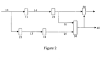
- Figure 2 shows a schematical signal flow diagram in an embodiment for corruption protected delayed lockstep CPUs.
- the input signal 10 is fed to the first CPU 11 and processed by the first CPU 11 to output the first output signal 14.
- the input signal 10 is also fed in parallel via the first delay unit 21 as the delayed input signal 13 to the second CPU 12 to output the second output signal 25.
- the second output signal 25 of the second CPU 12 is fed again to the comparator unit 30 to be compared with a correspondingly delayed version of the first output signal 14 in order to detect an error in the processing by the first CPU 11.
- a further second delay unit 23 not only delays the first output signal 14 to yield a further delayed first output signal 16 for the purpose of comparison of the further delayed first output signal 16 with the second output signal 25 by the comparator unit 30. Rather, the further second delay unit 23 applies a delay also to the first output signal 14 for the purpose of delaying the first output signal 14 in general before it may be further processed by subsequent stages.
- the further second delay unit 23 may delay a first output signal 14 related to a write transaction. In this way, there is enough time for the comparator unit 30 to detect an error in the processing by the first CPU 11 by comparing the second output signal 25 of the second CPU 12 with the further delayed first output signal 16 of the first CPU 11 before the corrupted first output signal 14 related to a write transaction may propagate to further stages of the system and corrupt them too.
- the system comprises an error blocking unit 50 adapted to receive the error signal 40 from the comparator unit 30.
- the error signal 40 from the comparator unit 30 may be used to block the further delayed first output signal 16 of the first CPU 11 from propagating into the subsequent parts of the system. As a result, in this case of an error in a write transaction, the integrity of the system may be maintained.
- embodiments may enable delaying write transactions to totally block them or to provide enough time to abort them. This may help multi-core systems to avoid corruption or to restrain it to known memory ranges so that part of the system can keep running.
- the further second delay unit 23 may be implemented in a lot of different ways.
- the further second delay unit 23 may delay all signals from the first CPU 11.
- the further second delay unit 23 may delay only signals related to write transactions.
- the further second delay unit 23 may delay only signals related to a category of write transactions.
- the further second delay unit 23 may delay signals related to write transactions to peripherals and memory attached to a shared internal bus and not delay signals related to write transactions to tightly coupled memories.
- error blocking unit 50 may be implemented in many different ways. In one embodiment, the error blocking unit 50 may actually block a write transaction originating from the first CPU 11 from further propagating through the system.
- the error blocking unit 50 may let a write transaction pass onto the system bus but then send a command to abort the write transaction as soon as an error is detected.
- the error blocking unit 50 may be adapted to modify the address of the write transaction to point to a reserved location or to a "safe" location reserved for that purpose.
- the write transaction may be protected by error detection/correction codes.
- the error blocking unit 50 may be adapted to corrupt the address signature of the write transaction which leads to an error at the target of the write transaction and which - ultimately - aborts the write transaction.
- Figure 3 shows an embodiment of a method for avoiding error propagation in a multi-CPU system.
- step 60 of the method an input signal is received by a first CPU.
- step 61 of the method the input signal is fed by a first delay unit to a second CPU.
- step 62 of the method at least one output signal of the first CPU related to write transactions of the first CPU is delayed by a second delay unit.
- step 63 of the method as shown in Figure 3 at least one output signal of the first CPU is compared by a comparator with at least one output signal of the second CPU.
- step 64 of the method as a result of the above comparison, it is determined if an error occurred during processing the input signal by the first or the second CPU to output a corresponding error signal.
- the error signal is used by an error blocking unit to modify a write transaction of the first CPU such that the error is kept from propagating through the system.
- a first embodiment relates to a system for avoiding error propagation in a multi-CPU system comprising a first CPU and at least one second CPU.
- the at least one second CPU is adapted to operate in delayed lockstep configuration with the first CPU to detect an error by comparing at least one output signal from the first CPU with at least one output signal from the at least one second CPU.
- this system comprises at least one delay unit adapted to delay at least one output signal of the first CPU related to a write transaction of the first CPU to modify at least one write transaction of the first CPU such that the error is kept from propagating through the system.
- the at least one delay unit is adapted to delay all output signals of the first CPU.
- the at least one delay unit is adapted to delay all output signals of the first CPU related to a write transaction of the first CPU.
- the at least one delay unit is adapted to delay at least one output signal of the first CPU related to a predetermined category of write transactions of the first CPU.
- the at least one delay unit is adapted to delay at least one output signal of the first CPU related to write transactions of the first CPU to peripherals and memory attached to a shared internal bus of the first CPU and the at least one second CPU.
- a further embodiment relates to a system comprising a first CPU coupled to receive an input signal, a second CPU and a first delay unit coupled to feed the input signal to the second CPU.
- a second delay unit is coupled to delay at least one output signal of the first CPU related to write transactions of the first CPU.
- said system comprises a comparator unit coupled to compare at least one output signal of the first CPU with at least one output signal of the second CPU to determine if an error occurred during processing the input signal by the first CPU or the second CPU, and output a corresponding error signal.
- said system comprises a protected error blocking unit coupled to use the error signal to modify - under a protection condition - a write transaction of the first CPU such that the error is kept from propagating through the system.
- the error blocking unit is protected in that the system further comprises a further comparator unit coupled to compare the at least one output signal of the first CPU with the at least one output signal of the second CPU.
- the purpose of the further comparator unit is to redundantly determine if an error occurred during processing the input signal by the first CPU or the second CPU, and output a corresponding negated error signal.
- the above system comprises a third comparator unit coupled to verify said protection condition that the error signal and the negated error signal correspondingly agree.
- the protection of the error blocking unit may help to provide a system that is fully compliant with the ISO26262 standard. Specifically, the protection may help to detect and avoid any dangerous situations where the error blocking unit might perform an "unintended" blocking in the absence of a lockstep error.
- the protected error blocking unit is adapted to block the write transaction of the first CPU from being executed.
- the protected error blocking unit is adapted to cause aborting the write transaction of the first CPU as soon as the error is determined.
- the protected error blocking unit is adapted to modify a write transaction address of the write transaction to point to a location reserved for fault containment.
- the protected error blocking unit is adapted to corrupt an address signature of the write transaction if the write transaction is protected by error detection/correction codes leading to an error at the target of the write transaction, and the target of the write transaction aborting the write transaction.
- a still further embodiment relates to a system comprising a processing unit and at least one further processing unit.
- the at least one further processing unit is adapted to process an input signal with a predetermined delay with respect to the processing unit to detect a processing error by comparison of predetermined output signals of the processing unit and the at least one further processing unit.
- this system comprises at least one delay unit adapted to delay at least one output signal of the processing unit to avoid unmodified propagation of at least one output signal of the processing unit through the system if a processing error has been detected.
- the at least one delay unit is adapted to delay at least one output signal of the processing unit related to a write transaction of the processing unit to modify at least one write transaction of the processing unit such that the processing error is kept from propagating through the system.
- system further comprises a protected error blocking unit coupled to use the result of said comparison of the predetermined output signals of the processing unit and the at least one further processing unit to modify - under a protection condition - a write transaction of the processing unit such that the processing error is kept from propagating through the system.
- the error blocking unit is protected in that the system further comprises means to perform a redundant comparison of the predetermined output signals of the processing unit and the at least one further processing unit to redundantly detect if a processing error occurred during processing the input signal by the processing unit or the at least one further processing unit.
- this embodiment comprises means to verify said protection condition that said comparison and said redundant comparison correspondingly agree.
- a delay provided by the at least one delay unit is long enough to enable aborting at least one write transaction of the processing unit.
- a further embodiment relates to a method for avoiding error propagation in a multi-CPU system with a first CPU and at least a second CPU.
- at least one second CPU is operated in delayed lockstep configuration with the first CPU to detect an error in form of at least one different processing result.
- At least one output signal of the first CPU related to a write transaction of the first CPU is delayed to modify at least one write transaction of the first CPU such that the error is kept from propagating through the system.
- delaying comprises delaying all output signals of the first CPU.
- delaying comprises delaying all output signals of the first CPU related to a write transaction of the first CPU.
- delaying comprises delaying at least one output signal of the first CPU related to a predetermined category of write transactions of the first CPU.
- delaying comprises delaying at least one output signal of the first CPU related to write transactions of the first CPU to peripherals and memory attached to a shared internal bus of the first CPU and the at least one second CPU.
- a further embodiment relates to a method for error containment in a system.
- This method comprises the step of processing an input signal by a processing unit and at least one further processing unit to detect an error in form of at least one different processing result.
- at least one output signal of the processing unit is delayed to enable - in case an error has been detected - modifying at least one output signal of the processing unit that would cause propagation of the error through the system.
- delaying comprises delaying at least one output signal of the processing unit related to a write transaction of the processing unit to modify at least one write transaction of the processing unit by an error block unit such that the detected error is kept from propagating through the system.
- modifying the at least one write transaction of the processing unit comprises blocking the write transaction of the first CPU from being executed.
- modifying the at least one write transaction of the processing unit comprises causing the write transaction of the first CPU to abort as soon as the error is detected.
- modifying the at least one write transaction of the processing unit comprises modifying at least one write transaction address of the at least one write transaction to point to a location reserved for fault containment.
- a further embodiment relates to a method for error containment in a system comprising a step of detecting an error by processing an input signal by multiple processing units.
- at least one output signal of a processing unit is delayed to enable - in case an error has been detected - modifying at least one output signal of the processing unit that would cause propagation of the error through the system.
Landscapes
- Engineering & Computer Science (AREA)
- Theoretical Computer Science (AREA)
- Quality & Reliability (AREA)
- Physics & Mathematics (AREA)
- General Engineering & Computer Science (AREA)
- General Physics & Mathematics (AREA)
- Hardware Redundancy (AREA)
Claims (8)
- System zum Vermeiden der Fehlerverbreitung in einem Mehr-CPU-System, mit:einer ersten CPU (11) und wenigstens einer zweiten CPU (12), wobei die wenigstens eine zweite CPU dazu ausgelegt ist, in einer verzögerten Gleichschritt-Konfiguration mit der ersten CPU zu arbeiten, um einen Fehler durch Vergleichen wenigstens eines Ausgangssignals von der ersten CPU (11), das von einer Verzögerungseinheit (23) verzögert wird, mit wenigstens einem Ausgangssignal von der wenigstens einen zweiten CPU (12), das nicht von einer Verzögerungseinheit verzögert wird, zu ermitteln,dadurch gekennzeichnet, dassdas von der Verzögerungseinheit (23) verzögerte Ausgangssignal an einen Komparator (30) geliefert wird, und zusätzlich an eine Fehlerblockiereinheit (50), um das Ausgangssignal, das sich auf eine Schreibtransaktion der ersten CPU (11) bezieht, durch Modifizieren einer Adresse der Schreibtransaktion zu modifizieren, um auf eine reservierte Stelle oder eine für diesen Zweck reservierte sichere Stelle zu zeigen.
- System nach Anspruch 1, wobei die Verzögerungseinheit dazu ausgelegt ist, alle Ausgangssignale der ersten CPU zu verzögern.
- System nach Anspruch 1, wobei die Verzögerungseinheit dazu ausgelegt ist, alle Ausgangssignale der ersten CPU, die sich auf eine Schreibtransaktion der ersten CPU beziehen, zu verzögern.
- System nach Anspruch 1, wobei die Verzögerungseinheit dazu ausgelegt ist, wenigstens ein Ausgangssignal der ersten CPU, das sich auf eine vorgegebene Kategorie von Schreibtransaktionen der ersten CPU bezieht, zu verzögern.
- System nach Anspruch 1, wobei die Verzögerungseinheit dazu ausgelegt ist, wenigstens ein Ausgangssignal der ersten CPU zu verzögern, das sich auf Schreibtransaktionen der ersten CPU an Peripheriegeräte und Speicher bezieht, die mit einem gemeinsamen internen Bus der ersten CPU und der wenigstens einen zweiten CPU verbunden sind.
- Verfahren zum Vermeiden der Fehlerverbreitung in einem Mehr-CPU-System mit einer ersten CPU und wenigstens einer zweiten CPU, wobei das Verfahren umfasst:Betreiben der wenigstens einen zweiten CPU (12) in einer verzögerten Gleichschritt-Konfiguration mit der ersten CPU (11), um einen Fehler in Form wenigstens eines unterschiedlichen Verarbeitungsergebnisses zu ermitteln; undVerzögern wenigstens eines Ausgangssignals der ersten CPU durch eine Verzögerungseinheit (23),gekennzeichnet durchVergleichen, durch einen Komparator (30), des Ausgangssignals der ersten CPU, das von der Verzögerungseinheit (23) verzögert wird, mit wenigstens einem Ausgangssignal von der wenigstens einen zweiten CPU (12), wobei das von der Verzögerungseinheit (23) verzögerte Ausgangssignal an den Komparator (30) geliefert wird, und zusätzlich an eine Fehlerblockiereinheit (50), um das Ausgangssignal, das sich auf eine Schreibtransaktion der ersten CPU (11) bezieht, durch Modifizieren einer Adresse der Schreibtransaktion zu modifizieren, um auf eine reservierte Stelle oder eine für diesen Zweck reservierte sichere Stelle zu zeigen.
- Verfahren nach Anspruch 6, wobei das Verzögern das Verzögern aller Ausgangssignale der ersten CPU umfasst.
- Verfahren nach Anspruch 6, wobei das Verzögern das Verzögern aller Ausgangssignale der ersten CPU umfasst, die sich auf eine Schreibtransaktion der ersten CPU beziehen.
Applications Claiming Priority (1)
| Application Number | Priority Date | Filing Date | Title |
|---|---|---|---|
| US13/417,382 US8819485B2 (en) | 2012-03-12 | 2012-03-12 | Method and system for fault containment |
Publications (2)
| Publication Number | Publication Date |
|---|---|
| EP2639699A1 EP2639699A1 (de) | 2013-09-18 |
| EP2639699B1 true EP2639699B1 (de) | 2015-08-05 |
Family
ID=47915390
Family Applications (1)
| Application Number | Title | Priority Date | Filing Date |
|---|---|---|---|
| EP13001212.3A Active EP2639699B1 (de) | 2012-03-12 | 2013-03-11 | Verfahren und System zur Fehlereindämmung |
Country Status (3)
| Country | Link |
|---|---|
| US (2) | US8819485B2 (de) |
| EP (1) | EP2639699B1 (de) |
| CN (1) | CN103309760A (de) |
Families Citing this family (14)
| Publication number | Priority date | Publication date | Assignee | Title |
|---|---|---|---|---|
| US8819485B2 (en) * | 2012-03-12 | 2014-08-26 | Infineon Technologies Ag | Method and system for fault containment |
| KR20140134376A (ko) * | 2013-05-14 | 2014-11-24 | 한국전자통신연구원 | 오류감지가 가능한 프로세서 및 이를 이용한 프로세서 코어 오류 감지 방법 |
| CN103544087B (zh) * | 2013-10-30 | 2015-10-28 | 中国航空工业集团公司第六三一研究所 | 一种锁步的处理器总线监控方法与计算机 |
| US10761925B2 (en) * | 2015-03-24 | 2020-09-01 | Nxp Usa, Inc. | Multi-channel network-on-a-chip |
| US10002056B2 (en) * | 2015-09-15 | 2018-06-19 | Texas Instruments Incorporated | Integrated circuit chip with cores asymmetrically oriented with respect to each other |
| US10331532B2 (en) * | 2017-01-19 | 2019-06-25 | Qualcomm Incorporated | Periodic non-intrusive diagnosis of lockstep systems |
| US10303566B2 (en) * | 2017-07-10 | 2019-05-28 | Arm Limited | Apparatus and method for checking output data during redundant execution of instructions |
| DE102018120328A1 (de) * | 2017-08-24 | 2019-02-28 | Infineon Technologies Ag | Sicherheitseinrichtung mit erweiterter Zuverlässigkeit |
| US10802932B2 (en) * | 2017-12-04 | 2020-10-13 | Nxp Usa, Inc. | Data processing system having lockstep operation |
| US10761561B2 (en) * | 2018-05-25 | 2020-09-01 | Arm Limited | Error checking for primary signal transmitted between first and second clock domains |
| US11424621B2 (en) | 2020-01-28 | 2022-08-23 | Qualcomm Incorporated | Configurable redundant systems for safety critical applications |
| US11636227B2 (en) * | 2020-11-16 | 2023-04-25 | Nxp B.V. | Protection against fault attacks by duplication |
| US11687428B2 (en) | 2021-01-20 | 2023-06-27 | Stmicroelectronics International N.V. | Glitch suppression apparatus and method |
| US11928475B2 (en) * | 2021-11-05 | 2024-03-12 | Ceremorphic, Inc. | Fast recovery for dual core lock step |
Family Cites Families (16)
| Publication number | Priority date | Publication date | Assignee | Title |
|---|---|---|---|---|
| US4635223A (en) | 1983-05-16 | 1987-01-06 | Motorola, Inc. | Fail safe protection circuitry for a commerical microprocessor in encryption equipment |
| JPH0721769B2 (ja) | 1988-08-12 | 1995-03-08 | 日本電気株式会社 | マイクロプロセッサの冗長構成による機能監視方式 |
| CN1168004C (zh) * | 1989-05-17 | 2004-09-22 | 国际商业机器公司 | 在数据处理系统中提供容错环境和体系结构的装置 |
| JPH05128080A (ja) | 1991-10-14 | 1993-05-25 | Mitsubishi Electric Corp | 情報処理装置 |
| US5748873A (en) * | 1992-09-17 | 1998-05-05 | Hitachi,Ltd. | Fault recovering system provided in highly reliable computer system having duplicated processors |
| GB2317032A (en) * | 1996-09-07 | 1998-03-11 | Motorola Gmbh | Microprocessor fail-safe system |
| GB2340627B (en) * | 1998-08-13 | 2000-10-04 | Plessey Telecomm | Data processing system |
| US6615366B1 (en) * | 1999-12-21 | 2003-09-02 | Intel Corporation | Microprocessor with dual execution core operable in high reliability mode |
| JP2003316599A (ja) * | 2002-02-22 | 2003-11-07 | Seiko Epson Corp | 集積回路 |
| DE102004038590A1 (de) | 2004-08-06 | 2006-03-16 | Robert Bosch Gmbh | Verfahren zur Verzögerung von Zugriffen auf Daten und/oder Befehle eines Zweirechnersystems sowie entsprechende Verzögerungseinheit |
| US20080244305A1 (en) * | 2007-03-30 | 2008-10-02 | Texas Instruments Deutschland, Gmbh | Delayed lock-step cpu compare |
| US20090177866A1 (en) * | 2008-01-08 | 2009-07-09 | Choate Michael L | System and method for functionally redundant computing system having a configurable delay between logically synchronized processors |
| US8019861B2 (en) * | 2009-01-29 | 2011-09-13 | Vmware, Inc. | Speculative virtual machine resource scheduling |
| US8275977B2 (en) * | 2009-04-08 | 2012-09-25 | Freescale Semiconductor, Inc. | Debug signaling in a multiple processor data processing system |
| US9146835B2 (en) * | 2012-01-05 | 2015-09-29 | International Business Machines Corporation | Methods and systems with delayed execution of multiple processors |
| US8819485B2 (en) * | 2012-03-12 | 2014-08-26 | Infineon Technologies Ag | Method and system for fault containment |
-
2012
- 2012-03-12 US US13/417,382 patent/US8819485B2/en active Active
-
2013
- 2013-03-11 EP EP13001212.3A patent/EP2639699B1/de active Active
- 2013-03-12 CN CN2013100775886A patent/CN103309760A/zh active Pending
-
2014
- 2014-07-22 US US14/337,699 patent/US9417946B2/en active Active
Also Published As
| Publication number | Publication date |
|---|---|
| US9417946B2 (en) | 2016-08-16 |
| US8819485B2 (en) | 2014-08-26 |
| US20140337670A1 (en) | 2014-11-13 |
| US20130238945A1 (en) | 2013-09-12 |
| EP2639699A1 (de) | 2013-09-18 |
| CN103309760A (zh) | 2013-09-18 |
Similar Documents
| Publication | Publication Date | Title |
|---|---|---|
| US9417946B2 (en) | Method and system for fault containment | |
| CN101243407B (zh) | 用于控制计算器系统的方法和装置 | |
| CN103262045B (zh) | 具有容错架构的微处理器系统 | |
| US20080163035A1 (en) | Method for Data Distribution and Data Distribution Unit in a Multiprocessor System | |
| US11392385B2 (en) | System and method for auto-recovery in lockstep processors | |
| US9207661B2 (en) | Dual core architecture of a control module of an engine | |
| US20180111626A1 (en) | Method and device for handling safety critical errors | |
| EP2824573B1 (de) | Mikrocomputertest | |
| US20080244305A1 (en) | Delayed lock-step cpu compare | |
| CN102640119B (zh) | 用于运行计算单元的方法 | |
| CN104346306B (zh) | 高完整性dma操作的系统和方法 | |
| US8954794B2 (en) | Method and system for detection of latent faults in microcontrollers | |
| US9218236B2 (en) | Error signal handling unit, device and method for outputting an error condition signal | |
| JP2012068788A (ja) | 情報処理装置、異常検出方法 | |
| JP2005215809A (ja) | コンピュータシステム、バスコントローラ及びそれらに用いるバス障害処理方法 | |
| KR101576848B1 (ko) | 에러 상태 신호를 출력하기 위한 에러 신호 처리 유닛, 장치 및 방법 | |
| CN112424753B (zh) | 多核系统 | |
| JP2011095837A (ja) | フェールセーフシステム | |
| CN107423029B (zh) | 计算单元 | |
| US20070294559A1 (en) | Method and Device for Delaying Access to Data and/or Instructions of a Multiprocessor System | |
| JP5287198B2 (ja) | 情報処理装置 | |
| Schneider et al. | Basic single-microcontroller monitoring concept for safety critical systems | |
| JP6668226B2 (ja) | 電子制御装置 | |
| JP2009093393A (ja) | データ処理装置及びデータ処理装置の自己診断方法 | |
| TS | Multi-Level Approaches of Fail Safe Techniques in Safety Critical Automotive Embedded Control Applications |
Legal Events
| Date | Code | Title | Description |
|---|---|---|---|
| PUAI | Public reference made under article 153(3) epc to a published international application that has entered the european phase |
Free format text: ORIGINAL CODE: 0009012 |
|
| AK | Designated contracting states |
Kind code of ref document: A1 Designated state(s): AL AT BE BG CH CY CZ DE DK EE ES FI FR GB GR HR HU IE IS IT LI LT LU LV MC MK MT NL NO PL PT RO RS SE SI SK SM TR |
|
| AX | Request for extension of the european patent |
Extension state: BA ME |
|
| 17P | Request for examination filed |
Effective date: 20140107 |
|
| RBV | Designated contracting states (corrected) |
Designated state(s): AL AT BE BG CH CY CZ DE DK EE ES FI FR GB GR HR HU IE IS IT LI LT LU LV MC MK MT NL NO PL PT RO RS SE SI SK SM TR |
|
| 17Q | First examination report despatched |
Effective date: 20140407 |
|
| GRAP | Despatch of communication of intention to grant a patent |
Free format text: ORIGINAL CODE: EPIDOSNIGR1 |
|
| RIC1 | Information provided on ipc code assigned before grant |
Ipc: G06F 11/16 20060101AFI20150219BHEP Ipc: G06F 11/07 20060101ALI20150219BHEP |
|
| INTG | Intention to grant announced |
Effective date: 20150316 |
|
| GRAS | Grant fee paid |
Free format text: ORIGINAL CODE: EPIDOSNIGR3 |
|
| GRAA | (expected) grant |
Free format text: ORIGINAL CODE: 0009210 |
|
| AK | Designated contracting states |
Kind code of ref document: B1 Designated state(s): AL AT BE BG CH CY CZ DE DK EE ES FI FR GB GR HR HU IE IS IT LI LT LU LV MC MK MT NL NO PL PT RO RS SE SI SK SM TR |
|
| REG | Reference to a national code |
Ref country code: GB Ref legal event code: FG4D |
|
| REG | Reference to a national code |
Ref country code: CH Ref legal event code: EP |
|
| REG | Reference to a national code |
Ref country code: AT Ref legal event code: REF Ref document number: 741065 Country of ref document: AT Kind code of ref document: T Effective date: 20150815 |
|
| REG | Reference to a national code |
Ref country code: IE Ref legal event code: FG4D |
|
| REG | Reference to a national code |
Ref country code: DE Ref legal event code: R096 Ref document number: 602013002465 Country of ref document: DE |
|
| REG | Reference to a national code |
Ref country code: AT Ref legal event code: MK05 Ref document number: 741065 Country of ref document: AT Kind code of ref document: T Effective date: 20150805 |
|
| REG | Reference to a national code |
Ref country code: LT Ref legal event code: MG4D |
|
| REG | Reference to a national code |
Ref country code: NL Ref legal event code: MP Effective date: 20150805 |
|
| PG25 | Lapsed in a contracting state [announced via postgrant information from national office to epo] |
Ref country code: NO Free format text: LAPSE BECAUSE OF FAILURE TO SUBMIT A TRANSLATION OF THE DESCRIPTION OR TO PAY THE FEE WITHIN THE PRESCRIBED TIME-LIMIT Effective date: 20151105 Ref country code: FI Free format text: LAPSE BECAUSE OF FAILURE TO SUBMIT A TRANSLATION OF THE DESCRIPTION OR TO PAY THE FEE WITHIN THE PRESCRIBED TIME-LIMIT Effective date: 20150805 Ref country code: LV Free format text: LAPSE BECAUSE OF FAILURE TO SUBMIT A TRANSLATION OF THE DESCRIPTION OR TO PAY THE FEE WITHIN THE PRESCRIBED TIME-LIMIT Effective date: 20150805 Ref country code: GR Free format text: LAPSE BECAUSE OF FAILURE TO SUBMIT A TRANSLATION OF THE DESCRIPTION OR TO PAY THE FEE WITHIN THE PRESCRIBED TIME-LIMIT Effective date: 20151106 Ref country code: LT Free format text: LAPSE BECAUSE OF FAILURE TO SUBMIT A TRANSLATION OF THE DESCRIPTION OR TO PAY THE FEE WITHIN THE PRESCRIBED TIME-LIMIT Effective date: 20150805 |
|
| PG25 | Lapsed in a contracting state [announced via postgrant information from national office to epo] |
Ref country code: SE Free format text: LAPSE BECAUSE OF FAILURE TO SUBMIT A TRANSLATION OF THE DESCRIPTION OR TO PAY THE FEE WITHIN THE PRESCRIBED TIME-LIMIT Effective date: 20150805 Ref country code: AT Free format text: LAPSE BECAUSE OF FAILURE TO SUBMIT A TRANSLATION OF THE DESCRIPTION OR TO PAY THE FEE WITHIN THE PRESCRIBED TIME-LIMIT Effective date: 20150805 Ref country code: IS Free format text: LAPSE BECAUSE OF FAILURE TO SUBMIT A TRANSLATION OF THE DESCRIPTION OR TO PAY THE FEE WITHIN THE PRESCRIBED TIME-LIMIT Effective date: 20151205 Ref country code: ES Free format text: LAPSE BECAUSE OF FAILURE TO SUBMIT A TRANSLATION OF THE DESCRIPTION OR TO PAY THE FEE WITHIN THE PRESCRIBED TIME-LIMIT Effective date: 20150805 Ref country code: HR Free format text: LAPSE BECAUSE OF FAILURE TO SUBMIT A TRANSLATION OF THE DESCRIPTION OR TO PAY THE FEE WITHIN THE PRESCRIBED TIME-LIMIT Effective date: 20150805 Ref country code: PT Free format text: LAPSE BECAUSE OF FAILURE TO SUBMIT A TRANSLATION OF THE DESCRIPTION OR TO PAY THE FEE WITHIN THE PRESCRIBED TIME-LIMIT Effective date: 20151207 Ref country code: PL Free format text: LAPSE BECAUSE OF FAILURE TO SUBMIT A TRANSLATION OF THE DESCRIPTION OR TO PAY THE FEE WITHIN THE PRESCRIBED TIME-LIMIT Effective date: 20150805 Ref country code: RS Free format text: LAPSE BECAUSE OF FAILURE TO SUBMIT A TRANSLATION OF THE DESCRIPTION OR TO PAY THE FEE WITHIN THE PRESCRIBED TIME-LIMIT Effective date: 20150805 |
|
| REG | Reference to a national code |
Ref country code: FR Ref legal event code: PLFP Year of fee payment: 4 |
|
| PG25 | Lapsed in a contracting state [announced via postgrant information from national office to epo] |
Ref country code: NL Free format text: LAPSE BECAUSE OF FAILURE TO SUBMIT A TRANSLATION OF THE DESCRIPTION OR TO PAY THE FEE WITHIN THE PRESCRIBED TIME-LIMIT Effective date: 20150805 |
|
| PG25 | Lapsed in a contracting state [announced via postgrant information from national office to epo] |
Ref country code: EE Free format text: LAPSE BECAUSE OF FAILURE TO SUBMIT A TRANSLATION OF THE DESCRIPTION OR TO PAY THE FEE WITHIN THE PRESCRIBED TIME-LIMIT Effective date: 20150805 Ref country code: DK Free format text: LAPSE BECAUSE OF FAILURE TO SUBMIT A TRANSLATION OF THE DESCRIPTION OR TO PAY THE FEE WITHIN THE PRESCRIBED TIME-LIMIT Effective date: 20150805 Ref country code: IT Free format text: LAPSE BECAUSE OF FAILURE TO SUBMIT A TRANSLATION OF THE DESCRIPTION OR TO PAY THE FEE WITHIN THE PRESCRIBED TIME-LIMIT Effective date: 20150805 Ref country code: CZ Free format text: LAPSE BECAUSE OF FAILURE TO SUBMIT A TRANSLATION OF THE DESCRIPTION OR TO PAY THE FEE WITHIN THE PRESCRIBED TIME-LIMIT Effective date: 20150805 Ref country code: SK Free format text: LAPSE BECAUSE OF FAILURE TO SUBMIT A TRANSLATION OF THE DESCRIPTION OR TO PAY THE FEE WITHIN THE PRESCRIBED TIME-LIMIT Effective date: 20150805 |
|
| REG | Reference to a national code |
Ref country code: DE Ref legal event code: R097 Ref document number: 602013002465 Country of ref document: DE |
|
| PG25 | Lapsed in a contracting state [announced via postgrant information from national office to epo] |
Ref country code: RO Free format text: LAPSE BECAUSE OF FAILURE TO SUBMIT A TRANSLATION OF THE DESCRIPTION OR TO PAY THE FEE WITHIN THE PRESCRIBED TIME-LIMIT Effective date: 20150805 |
|
| PLBE | No opposition filed within time limit |
Free format text: ORIGINAL CODE: 0009261 |
|
| STAA | Information on the status of an ep patent application or granted ep patent |
Free format text: STATUS: NO OPPOSITION FILED WITHIN TIME LIMIT |
|
| 26N | No opposition filed |
Effective date: 20160509 |
|
| PG25 | Lapsed in a contracting state [announced via postgrant information from national office to epo] |
Ref country code: BE Free format text: LAPSE BECAUSE OF NON-PAYMENT OF DUE FEES Effective date: 20160331 Ref country code: SI Free format text: LAPSE BECAUSE OF FAILURE TO SUBMIT A TRANSLATION OF THE DESCRIPTION OR TO PAY THE FEE WITHIN THE PRESCRIBED TIME-LIMIT Effective date: 20150805 |
|
| PG25 | Lapsed in a contracting state [announced via postgrant information from national office to epo] |
Ref country code: LU Free format text: LAPSE BECAUSE OF FAILURE TO SUBMIT A TRANSLATION OF THE DESCRIPTION OR TO PAY THE FEE WITHIN THE PRESCRIBED TIME-LIMIT Effective date: 20160311 Ref country code: MC Free format text: LAPSE BECAUSE OF FAILURE TO SUBMIT A TRANSLATION OF THE DESCRIPTION OR TO PAY THE FEE WITHIN THE PRESCRIBED TIME-LIMIT Effective date: 20150805 |
|
| REG | Reference to a national code |
Ref country code: CH Ref legal event code: PL |
|
| REG | Reference to a national code |
Ref country code: IE Ref legal event code: MM4A |
|
| PG25 | Lapsed in a contracting state [announced via postgrant information from national office to epo] |
Ref country code: BE Free format text: LAPSE BECAUSE OF FAILURE TO SUBMIT A TRANSLATION OF THE DESCRIPTION OR TO PAY THE FEE WITHIN THE PRESCRIBED TIME-LIMIT Effective date: 20150805 |
|
| PG25 | Lapsed in a contracting state [announced via postgrant information from national office to epo] |
Ref country code: CH Free format text: LAPSE BECAUSE OF NON-PAYMENT OF DUE FEES Effective date: 20160331 Ref country code: LI Free format text: LAPSE BECAUSE OF NON-PAYMENT OF DUE FEES Effective date: 20160331 Ref country code: IE Free format text: LAPSE BECAUSE OF NON-PAYMENT OF DUE FEES Effective date: 20160311 |
|
| REG | Reference to a national code |
Ref country code: FR Ref legal event code: PLFP Year of fee payment: 5 |
|
| PG25 | Lapsed in a contracting state [announced via postgrant information from national office to epo] |
Ref country code: MT Free format text: LAPSE BECAUSE OF FAILURE TO SUBMIT A TRANSLATION OF THE DESCRIPTION OR TO PAY THE FEE WITHIN THE PRESCRIBED TIME-LIMIT Effective date: 20150805 |
|
| GBPC | Gb: european patent ceased through non-payment of renewal fee |
Effective date: 20170311 |
|
| PG25 | Lapsed in a contracting state [announced via postgrant information from national office to epo] |
Ref country code: GB Free format text: LAPSE BECAUSE OF NON-PAYMENT OF DUE FEES Effective date: 20170311 |
|
| REG | Reference to a national code |
Ref country code: FR Ref legal event code: PLFP Year of fee payment: 6 |
|
| PG25 | Lapsed in a contracting state [announced via postgrant information from national office to epo] |
Ref country code: HU Free format text: LAPSE BECAUSE OF FAILURE TO SUBMIT A TRANSLATION OF THE DESCRIPTION OR TO PAY THE FEE WITHIN THE PRESCRIBED TIME-LIMIT; INVALID AB INITIO Effective date: 20130311 Ref country code: CY Free format text: LAPSE BECAUSE OF FAILURE TO SUBMIT A TRANSLATION OF THE DESCRIPTION OR TO PAY THE FEE WITHIN THE PRESCRIBED TIME-LIMIT Effective date: 20150805 Ref country code: SM Free format text: LAPSE BECAUSE OF FAILURE TO SUBMIT A TRANSLATION OF THE DESCRIPTION OR TO PAY THE FEE WITHIN THE PRESCRIBED TIME-LIMIT Effective date: 20150805 |
|
| PG25 | Lapsed in a contracting state [announced via postgrant information from national office to epo] |
Ref country code: MT Free format text: LAPSE BECAUSE OF FAILURE TO SUBMIT A TRANSLATION OF THE DESCRIPTION OR TO PAY THE FEE WITHIN THE PRESCRIBED TIME-LIMIT Effective date: 20160331 Ref country code: TR Free format text: LAPSE BECAUSE OF FAILURE TO SUBMIT A TRANSLATION OF THE DESCRIPTION OR TO PAY THE FEE WITHIN THE PRESCRIBED TIME-LIMIT Effective date: 20150805 Ref country code: MK Free format text: LAPSE BECAUSE OF FAILURE TO SUBMIT A TRANSLATION OF THE DESCRIPTION OR TO PAY THE FEE WITHIN THE PRESCRIBED TIME-LIMIT Effective date: 20150805 |
|
| PG25 | Lapsed in a contracting state [announced via postgrant information from national office to epo] |
Ref country code: BG Free format text: LAPSE BECAUSE OF FAILURE TO SUBMIT A TRANSLATION OF THE DESCRIPTION OR TO PAY THE FEE WITHIN THE PRESCRIBED TIME-LIMIT Effective date: 20150805 |
|
| PG25 | Lapsed in a contracting state [announced via postgrant information from national office to epo] |
Ref country code: AL Free format text: LAPSE BECAUSE OF FAILURE TO SUBMIT A TRANSLATION OF THE DESCRIPTION OR TO PAY THE FEE WITHIN THE PRESCRIBED TIME-LIMIT Effective date: 20150805 |
|
| PGFP | Annual fee paid to national office [announced via postgrant information from national office to epo] |
Ref country code: FR Payment date: 20230327 Year of fee payment: 11 |
|
| P01 | Opt-out of the competence of the unified patent court (upc) registered |
Effective date: 20230528 |
|
| PG25 | Lapsed in a contracting state [announced via postgrant information from national office to epo] |
Ref country code: FR Free format text: LAPSE BECAUSE OF NON-PAYMENT OF DUE FEES Effective date: 20240331 |
|
| PG25 | Lapsed in a contracting state [announced via postgrant information from national office to epo] |
Ref country code: FR Free format text: LAPSE BECAUSE OF NON-PAYMENT OF DUE FEES Effective date: 20240331 |
|
| PGFP | Annual fee paid to national office [announced via postgrant information from national office to epo] |
Ref country code: DE Payment date: 20250521 Year of fee payment: 13 |