EP2637219B1 - Junction box for a photovoltaic solar panel - Google Patents
Junction box for a photovoltaic solar panel Download PDFInfo
- Publication number
- EP2637219B1 EP2637219B1 EP13170289.6A EP13170289A EP2637219B1 EP 2637219 B1 EP2637219 B1 EP 2637219B1 EP 13170289 A EP13170289 A EP 13170289A EP 2637219 B1 EP2637219 B1 EP 2637219B1
- Authority
- EP
- European Patent Office
- Prior art keywords
- junction box
- coupling
- lid
- solar panel
- top wall
- Prior art date
- Legal status (The legal status is an assumption and is not a legal conclusion. Google has not performed a legal analysis and makes no representation as to the accuracy of the status listed.)
- Not-in-force
Links
- 229910000679 solder Inorganic materials 0.000 claims description 91
- 230000008878 coupling Effects 0.000 claims description 66
- 238000010168 coupling process Methods 0.000 claims description 66
- 238000005859 coupling reaction Methods 0.000 claims description 66
- 239000000463 material Substances 0.000 claims description 35
- 238000000034 method Methods 0.000 claims description 15
- 238000004519 manufacturing process Methods 0.000 claims description 8
- 239000000853 adhesive Substances 0.000 claims description 7
- 230000001070 adhesive effect Effects 0.000 claims description 7
- 238000005452 bending Methods 0.000 description 7
- 239000011521 glass Substances 0.000 description 7
- XLYOFNOQVPJJNP-UHFFFAOYSA-N water Substances O XLYOFNOQVPJJNP-UHFFFAOYSA-N 0.000 description 7
- 239000006260 foam Substances 0.000 description 4
- 239000004033 plastic Substances 0.000 description 4
- 229920003023 plastic Polymers 0.000 description 4
- 238000007789 sealing Methods 0.000 description 4
- 238000003466 welding Methods 0.000 description 4
- 230000007423 decrease Effects 0.000 description 3
- 238000002347 injection Methods 0.000 description 3
- 239000007924 injection Substances 0.000 description 3
- 230000003647 oxidation Effects 0.000 description 3
- 238000007254 oxidation reaction Methods 0.000 description 3
- 239000004417 polycarbonate Substances 0.000 description 3
- 229920000515 polycarbonate Polymers 0.000 description 3
- RNFJDJUURJAICM-UHFFFAOYSA-N 2,2,4,4,6,6-hexaphenoxy-1,3,5-triaza-2$l^{5},4$l^{5},6$l^{5}-triphosphacyclohexa-1,3,5-triene Chemical compound N=1P(OC=2C=CC=CC=2)(OC=2C=CC=CC=2)=NP(OC=2C=CC=CC=2)(OC=2C=CC=CC=2)=NP=1(OC=1C=CC=CC=1)OC1=CC=CC=C1 RNFJDJUURJAICM-UHFFFAOYSA-N 0.000 description 2
- 229920004142 LEXAN™ Polymers 0.000 description 2
- 239000004418 Lexan Substances 0.000 description 2
- 238000013005 condensation curing Methods 0.000 description 2
- 230000000694 effects Effects 0.000 description 2
- 239000003063 flame retardant Substances 0.000 description 2
- 238000004382 potting Methods 0.000 description 2
- 229920002379 silicone rubber Polymers 0.000 description 2
- 239000004945 silicone rubber Substances 0.000 description 2
- 229910001369 Brass Inorganic materials 0.000 description 1
- 229910000906 Bronze Inorganic materials 0.000 description 1
- RYGMFSIKBFXOCR-UHFFFAOYSA-N Copper Chemical compound [Cu] RYGMFSIKBFXOCR-UHFFFAOYSA-N 0.000 description 1
- 239000004831 Hot glue Substances 0.000 description 1
- XUIMIQQOPSSXEZ-UHFFFAOYSA-N Silicon Chemical compound [Si] XUIMIQQOPSSXEZ-UHFFFAOYSA-N 0.000 description 1
- 239000004411 aluminium Substances 0.000 description 1
- XAGFODPZIPBFFR-UHFFFAOYSA-N aluminium Chemical compound [Al] XAGFODPZIPBFFR-UHFFFAOYSA-N 0.000 description 1
- 229910052782 aluminium Inorganic materials 0.000 description 1
- 239000010951 brass Substances 0.000 description 1
- 239000010974 bronze Substances 0.000 description 1
- 150000001875 compounds Chemical class 0.000 description 1
- 238000009833 condensation Methods 0.000 description 1
- 230000005494 condensation Effects 0.000 description 1
- 239000010949 copper Substances 0.000 description 1
- 229910052802 copper Inorganic materials 0.000 description 1
- KUNSUQLRTQLHQQ-UHFFFAOYSA-N copper tin Chemical compound [Cu].[Sn] KUNSUQLRTQLHQQ-UHFFFAOYSA-N 0.000 description 1
- 230000007797 corrosion Effects 0.000 description 1
- 238000005260 corrosion Methods 0.000 description 1
- 238000009826 distribution Methods 0.000 description 1
- 230000007613 environmental effect Effects 0.000 description 1
- 239000012943 hotmelt Substances 0.000 description 1
- 238000003780 insertion Methods 0.000 description 1
- 230000037431 insertion Effects 0.000 description 1
- 239000007788 liquid Substances 0.000 description 1
- 230000007257 malfunction Effects 0.000 description 1
- 230000007935 neutral effect Effects 0.000 description 1
- 229910052710 silicon Inorganic materials 0.000 description 1
- 239000010703 silicon Substances 0.000 description 1
Images






Classifications
-
- H—ELECTRICITY
- H01—ELECTRIC ELEMENTS
- H01R—ELECTRICALLY-CONDUCTIVE CONNECTIONS; STRUCTURAL ASSOCIATIONS OF A PLURALITY OF MUTUALLY-INSULATED ELECTRICAL CONNECTING ELEMENTS; COUPLING DEVICES; CURRENT COLLECTORS
- H01R13/00—Details of coupling devices of the kinds covered by groups H01R12/70 or H01R24/00 - H01R33/00
- H01R13/66—Structural association with built-in electrical component
- H01R13/6608—Structural association with built-in electrical component with built-in single component
- H01R13/6641—Structural association with built-in electrical component with built-in single component with diode
-
- H—ELECTRICITY
- H10—SEMICONDUCTOR DEVICES; ELECTRIC SOLID-STATE DEVICES NOT OTHERWISE PROVIDED FOR
- H10F—INORGANIC SEMICONDUCTOR DEVICES SENSITIVE TO INFRARED RADIATION, LIGHT, ELECTROMAGNETIC RADIATION OF SHORTER WAVELENGTH OR CORPUSCULAR RADIATION
- H10F19/00—Integrated devices, or assemblies of multiple devices, comprising at least one photovoltaic cell covered by group H10F10/00, e.g. photovoltaic modules
- H10F19/80—Encapsulations or containers for integrated devices, or assemblies of multiple devices, having photovoltaic cells
-
- H—ELECTRICITY
- H02—GENERATION; CONVERSION OR DISTRIBUTION OF ELECTRIC POWER
- H02S—GENERATION OF ELECTRIC POWER BY CONVERSION OF INFRARED RADIATION, VISIBLE LIGHT OR ULTRAVIOLET LIGHT, e.g. USING PHOTOVOLTAIC [PV] MODULES
- H02S40/00—Components or accessories in combination with PV modules, not provided for in groups H02S10/00 - H02S30/00
- H02S40/30—Electrical components
- H02S40/34—Electrical components comprising specially adapted electrical connection means to be structurally associated with the PV module, e.g. junction boxes
-
- H—ELECTRICITY
- H01—ELECTRIC ELEMENTS
- H01R—ELECTRICALLY-CONDUCTIVE CONNECTIONS; STRUCTURAL ASSOCIATIONS OF A PLURALITY OF MUTUALLY-INSULATED ELECTRICAL CONNECTING ELEMENTS; COUPLING DEVICES; CURRENT COLLECTORS
- H01R11/00—Individual connecting elements providing two or more spaced connecting locations for conductive members which are, or may be, thereby interconnected, e.g. end pieces for wires or cables supported by the wire or cable and having means for facilitating electrical connection to some other wire, terminal, or conductive member, blocks of binding posts
- H01R11/03—Individual connecting elements providing two or more spaced connecting locations for conductive members which are, or may be, thereby interconnected, e.g. end pieces for wires or cables supported by the wire or cable and having means for facilitating electrical connection to some other wire, terminal, or conductive member, blocks of binding posts characterised by the relationship between the connecting locations
- H01R11/09—Individual connecting elements providing two or more spaced connecting locations for conductive members which are, or may be, thereby interconnected, e.g. end pieces for wires or cables supported by the wire or cable and having means for facilitating electrical connection to some other wire, terminal, or conductive member, blocks of binding posts characterised by the relationship between the connecting locations the connecting locations being identical
-
- H—ELECTRICITY
- H01—ELECTRIC ELEMENTS
- H01R—ELECTRICALLY-CONDUCTIVE CONNECTIONS; STRUCTURAL ASSOCIATIONS OF A PLURALITY OF MUTUALLY-INSULATED ELECTRICAL CONNECTING ELEMENTS; COUPLING DEVICES; CURRENT COLLECTORS
- H01R31/00—Coupling parts supported only by co-operation with counterpart
- H01R31/06—Intermediate parts for linking two coupling parts, e.g. adapter
- H01R31/065—Intermediate parts for linking two coupling parts, e.g. adapter with built-in electric apparatus
-
- Y—GENERAL TAGGING OF NEW TECHNOLOGICAL DEVELOPMENTS; GENERAL TAGGING OF CROSS-SECTIONAL TECHNOLOGIES SPANNING OVER SEVERAL SECTIONS OF THE IPC; TECHNICAL SUBJECTS COVERED BY FORMER USPC CROSS-REFERENCE ART COLLECTIONS [XRACs] AND DIGESTS
- Y02—TECHNOLOGIES OR APPLICATIONS FOR MITIGATION OR ADAPTATION AGAINST CLIMATE CHANGE
- Y02E—REDUCTION OF GREENHOUSE GAS [GHG] EMISSIONS, RELATED TO ENERGY GENERATION, TRANSMISSION OR DISTRIBUTION
- Y02E10/00—Energy generation through renewable energy sources
- Y02E10/50—Photovoltaic [PV] energy
-
- Y—GENERAL TAGGING OF NEW TECHNOLOGICAL DEVELOPMENTS; GENERAL TAGGING OF CROSS-SECTIONAL TECHNOLOGIES SPANNING OVER SEVERAL SECTIONS OF THE IPC; TECHNICAL SUBJECTS COVERED BY FORMER USPC CROSS-REFERENCE ART COLLECTIONS [XRACs] AND DIGESTS
- Y10—TECHNICAL SUBJECTS COVERED BY FORMER USPC
- Y10T—TECHNICAL SUBJECTS COVERED BY FORMER US CLASSIFICATION
- Y10T29/00—Metal working
- Y10T29/49—Method of mechanical manufacture
- Y10T29/49002—Electrical device making
- Y10T29/49117—Conductor or circuit manufacturing
-
- Y—GENERAL TAGGING OF NEW TECHNOLOGICAL DEVELOPMENTS; GENERAL TAGGING OF CROSS-SECTIONAL TECHNOLOGIES SPANNING OVER SEVERAL SECTIONS OF THE IPC; TECHNICAL SUBJECTS COVERED BY FORMER USPC CROSS-REFERENCE ART COLLECTIONS [XRACs] AND DIGESTS
- Y10—TECHNICAL SUBJECTS COVERED BY FORMER USPC
- Y10T—TECHNICAL SUBJECTS COVERED BY FORMER US CLASSIFICATION
- Y10T29/00—Metal working
- Y10T29/49—Method of mechanical manufacture
- Y10T29/49002—Electrical device making
- Y10T29/49117—Conductor or circuit manufacturing
- Y10T29/49204—Contact or terminal manufacturing
- Y10T29/49208—Contact or terminal manufacturing by assembling plural parts
-
- Y—GENERAL TAGGING OF NEW TECHNOLOGICAL DEVELOPMENTS; GENERAL TAGGING OF CROSS-SECTIONAL TECHNOLOGIES SPANNING OVER SEVERAL SECTIONS OF THE IPC; TECHNICAL SUBJECTS COVERED BY FORMER USPC CROSS-REFERENCE ART COLLECTIONS [XRACs] AND DIGESTS
- Y10—TECHNICAL SUBJECTS COVERED BY FORMER USPC
- Y10T—TECHNICAL SUBJECTS COVERED BY FORMER US CLASSIFICATION
- Y10T29/00—Metal working
- Y10T29/49—Method of mechanical manufacture
- Y10T29/49002—Electrical device making
- Y10T29/49117—Conductor or circuit manufacturing
- Y10T29/49204—Contact or terminal manufacturing
- Y10T29/49208—Contact or terminal manufacturing by assembling plural parts
- Y10T29/49222—Contact or terminal manufacturing by assembling plural parts forming array of contacts or terminals
Definitions
- the invention relates to a device for affixing to a photovoltaic solar panel module in order to provide a connection between solar panel modules of a photovoltaic array or a connection between solar panel modules and other devices such as a bus system or cables.
- the lid comprises further embossments that are arranged such that they extend through the opening into the interior space when being mounted onto the housing. Due to said further embossments filling material is forced to flow through the opening into the overflow space, when said lid is mounted onto the housing when filled fully with filling material.
- a method for manufacturing a junction box according to one of the claims 1 to 10 comprises the steps of
- junction box With such a method a pre-mounted junction box is provided. Said junction box can be mounted on a solar panel.
- the resilient zone is designed as a bending structure, wherein bending of said bending structure results in said adjustment. This allows an easy adjustment of the length.
- the housing 1 comprises sidewalls (here a first sidewall 11 and a second sidewall 12) and a top wall 13.
- the sidewalls 11, 12 extend from the top wall 13.
- An interior space 10 is defined by said sidewalls 11, 12 and said top wall 13.
- Said interior space 10 is provided to accommodate electrical contact elements which are in an electrical contact with a solar cell of a solar panel.
- the interior space 10 shall be sealed off from environmental influences such as water, air etc. to prevent oxidation of the electrical contact elements.
- the terms external and internal will be used.
- the term external or exterior space is to be understood that it comprises everything that is arranged outside of the housing 1, whereas the term internal is to be understood as to comprise everything that is arranged within the interior space 10.
- Figure 9a - 9d illustrate a method for manufacturing a junction box according to the present invention.
- solder tail 9 which may also be designated as solder element or solder tag can be used not only with the junction box as described herein, but with every other electrical device. The same applies to the solder tail 7 as it is described above.
- the contact zone 91 is provided to establish an electrical contact with a first electrical device (e.g. the first contact element 5 or second contact element 6).
- a first electrical device e.g. the first contact element 5 or second contact element 6
- the contact zone 91 is designed such that it may be connected to the electrical device by means of a solder connection, welded connection or a crimped connection etc.
- the contact zone 91 is formed as tubular body 910.
- Said tubular body 910 comprises a first end having several cut outs 911 and a lid portion 912 and a second end on which the resilient zone 92 is formed.
- the contact zone 91 can also be designated as being cylindrical.
- the term cylindrical is to be understood as having a circular, rectangular, oval, triangular or elliptical shaped as viewed along axis A.
- the solder zone 94 is provided to establish an electrical contact with a second electrical device (e.g. a solar panel). Said solder zone 94 extends from the transfer zone 93. In the present example there is one solder zone 94 arranged but in other examples it is also possible to arranged more than one solder zone 94.
- the solder zone 94 here extends angular from the tubular body of the transfer zone 93.
Landscapes
- Photovoltaic Devices (AREA)
- Engineering & Computer Science (AREA)
- Manufacturing & Machinery (AREA)
- Connections Effected By Soldering, Adhesion, Or Permanent Deformation (AREA)
- Coupling Device And Connection With Printed Circuit (AREA)
Description
- The invention relates to a device for affixing to a photovoltaic solar panel module in order to provide a connection between solar panel modules of a photovoltaic array or a connection between solar panel modules and other devices such as a bus system or cables.
- Such devices are also known under the designation junction boxes or connection boxes. Such junction boxes are well known from prior art. Usually said junction boxes provide an electrical contact between contacts of a photovoltaic solar panel and cables which are connected to a further photovoltaic solar panel or to any other device, such as a distribution box or a bus system
-
EP 1 501 157 shows an example of such a junction box. Contacts of a solar panel extend above the surface on which the junction box is arranged and protrude through openings into the interior of the junction box. Said contacts are received by a contact element that is arranged in the interior of the junction box. Furthermore the junction box comprises openings through which cables can be inserted into the interior of the junction box in order to be received by said contact element. The contact element provides an electrical contact between the contacts of a solar panel and the wire. Said junction box further comprises an opening in order to provide access to the interior of the box. The opening is sealed by means of a sealing ring and a lid. -
US 4 654 470 is another example of a junction box. - Since the solar panels are usually exposed to effects of weather such as rain, snow, wind etc. it is particularly important that the junction boxes or connecting boxes have weatherproof properties. Such weatherproof properties include the resistance against moisture, water or temperature differences.
- The inflow of water into the interior of such a junction box should be avoided under any circumstances, since it may cause short circuits and/or lead to corrosion of the metallic connection elements. The presence of water in the interior of a junction box is not only a result from water that enters through leaky portions of the junction box, but may also be the result of water condensation. However, the presence of water decreases the operational reliability and the lifetime of such a junction box.
- Furthermore junction boxes are exposed to thermal differences that result in thermal expansion of the junction box itself. Such an expansion can lead to a malfunction of a sealing element, such as the above mentioned sealing ring.
- Usually such an expansion leads to mechanical stresses which may lead to cracks in the boxes. Especially sensitive to such mechanical stresses are glued sections.
- A further drawback of devices according to prior art is the manufacturing process. Still a high percentage of such a box is manufactured by hand. This leads to high costs. Furthermore quality issues may also arise, since precision and reliability of each craftsman is variable.
- Quite often the electrical connection of the electrical contacts between the junction box and the solar panel are designed as a spring contacts. Such spring contacts are susceptible to oxidation and mechanical influences. Said negative influences can lower the efficiency of a solar panel arrangement.
- An object of the present invention is to provide a junction box, which does not have the disadvantages of the junction boxes known from prior art. In particular the junction box shall have an enhanced lifetime.
- This object is achieved by a junction box having the features of claim 1. Accordingly a junction box for a solar panel comprises a housing, a lid, a first coupling and a second coupling. The housing comprises sidewalls and a top wall defining an interior space. The first coupling comprises a first contact element and the second coupling comprises a second contact element. Said contact elements penetrate at least one of the sidewalls, so that the contact elements provide an electrical contact from external contact elements to internal contact elements, such as solder tails. Internal contact elements are arranged at least partially in said interior space. The top wall comprises an opening extending only partially in said top wall. Said opening is located such in the top wall that access to said internal contact elements, such as said solder tails in a perpendicular direction to the surface of a solar panel for connecting the solder tail to the solar panel is provided. The couplings are arranged angular to each other, as defined in the characterizing part of claim 1.
- Due to the specific arrangement of the couplings the cables to be connected can be guided in an advantageous manner so that mechanical stress from the cable on the junction box can be reduced:
- Preferably the top wall comprises an outer sidewall that extends perpendicular from the top wall and that surrounds the outer circumference of the top wall, so that an overflow space is defined by the top wall and the outer sidewall.
- Preferably the opening is surrounded by an inner sidewall which extends perpendicular from said top wall. Such a sidewall limits the overflow space to the opening.
- If the interior space is filled with a filling material excess filling material may flow into the overflow space defined by the top wall, the outer sidewall and the inner sidewall. The filling material is preferably a potting compound (pottant) or a foam.
- Preferably filling material is injectable into the interior space through said opening, so that the interior space is fully filled with said filling material, and in that the opening is closeable with the lid. Preferably the filling material is a material that is injected in a liquid state and hardens after being injected. Preferably the filling material is a pottant or a foam.
- Preferably the lid comprises a wall extending perpendicular to the lid and having a shape that fits into the opening in the top surface.
- Such a wall provides a good and easily sealable contact between the opening and the lid.
- Preferably the lid comprises further embossments that are arranged such that they extend through the opening into the interior space when being mounted onto the housing. Due to said further embossments filling material is forced to flow through the opening into the overflow space, when said lid is mounted onto the housing when filled fully with filling material.
- Due to that overflow the lid is connected to the housing in tightly sealed manner. The embossments are advantageous, since they reduce the volume in the interior space so that filling material and air that may be present is forced out of the interior space. Additionally a closure force is provided.
- A method for manufacturing a junction box according to one of the claims 1 to 10 comprises the steps of
- providing the first coupling with a first contact element and the second coupling with a second contact element;
- connecting the first coupling and the second coupling with the housing;
- providing each of the contact elements with a solder tail;
- affixing the diode at the first contact element and at the second contact element
- With such a method a pre-mounted junction box is provided. Said junction box can be mounted on a solar panel.
- A method for providing a solar panel with a junction box according to one of the claims 1 to 10 comprises the steps of:
- Applying adhesive to the junction box base perimeter or flange;
- arranging the junction box on a surface of a solar panel module;
- affixing solder tail to the contacts of a solar panel;
- filling the interior space of the housing with a filling material; and
- mounting the lid on the top wall, so that parts of the lid, extend into the interior space of the housing.
- Thereby the pre-assembled junction box can be mounted onto a solar panel in an effective and automatic manner. The arrangement of the opening giving access to the solder tail is a particular advantage in terms of automatic manufacturing.
- An example of a solder element which is not part of the invention for providing an electrical connection between a first electrical device and a second electrical device comprises a cylindrically shaped contact zone to be contacted to the first electrical device, a resilient zone and a cylindrically shaped transfer zone having a solder zone to be contacted to the second electrical device. The axes of the contact zone and of the transfer zone are axially arranged in alignment of a longitudinal axis. The resilient zone enables adjustment of the axial distance between the contact zone and the solder zone.
- Such a solder element is particularly advantageous as the adjustment of the length enables the solder element to be used in a flexible manner.
- Preferably the resilient zone is arranged between the contact zone and the solder zone.
- Preferably the resilient zone is designed as a bending structure, wherein bending of said bending structure results in said adjustment. This allows an easy adjustment of the length.
- The resilient section comprises at least one, preferably at least two, even more preferably at least three to six, resilient web.
- Preferably the solder element is produced by a stamping and/or forming process.
- The drawings will be explained in greater detail by means of a description of an exemplary embodiment, with reference to the following figures:
- Fig. 1
- shows a perspective view of a junction box according to the present invention with a lid according to the present invention;
- Fig. 2
- shows a bottom view of the junction box of
figure 1 ; - Fig. 3
- shows a top view of the junction box of
figure 1 ; - Fig. 4
- shows a side view of the junction box of
figure 1 ; - Fig. 5 a-b
- show a perspective view of the lid for the junction box according to
figure 1 ; - Fig. 6 a-b
- show the junction box according to
figure 1 without a lid; - Fig. 7 a-b
- show a connector element that is arranged in the junction box;
- Fig. 8 a-b
- show the connector element of
Fig. 7 with a coupling element; - Fig. 9 a-d
- show assembly steps of a junction box according to the present invention;
- Fig. 10 a-c
- show views of a junction box of a further embodiment according to the present invention;
- Fig. 11 a-d
- show views of a solder element which is not part of the invention and
- Fig. 12 a, b
- show views of a weather cover or junction box according to a further embodiment.
- With reference to the drawings possible embodiments are described. The drawings and the description illustrate preferred embodiments and shall not be construed to limit the invention, which is defined by the claims.
-
Figures 1 to 4 show a junction box according to the present invention. Such a junction box comprises preferably a housing 1, alid 2, afirst coupling 3 and asecond coupling 4. The junction box according to the present invention is used to provide an electrical contact between a solar cell of solar panel and external contact elements such as cables etc. or other solar cells. Such solar panels have a typical size of 2200 mm x 2600 mm, but can also be smaller or larger. With such solar panels voltages between 70 V and 500 V and currents between 0.1 amps and 10 amps can be produced. However, the junction box according to the present invention can also be used for solar panels providing higher or lower currents or voltages, respectively. - The housing 1 comprises sidewalls (here a
first sidewall 11 and a second sidewall 12) and atop wall 13. Thesidewalls top wall 13. Aninterior space 10 is defined by said sidewalls 11, 12 and saidtop wall 13. Saidinterior space 10 is provided to accommodate electrical contact elements which are in an electrical contact with a solar cell of a solar panel. When the junction box is mounted on a solar panel theinterior space 10 shall be sealed off from environmental influences such as water, air etc. to prevent oxidation of the electrical contact elements. Afterwards the terms external and internal will be used. The term external or exterior space is to be understood that it comprises everything that is arranged outside of the housing 1, whereas the term internal is to be understood as to comprise everything that is arranged within theinterior space 10. - Preferably the housing 1 is made of plastics. Preferably polycarbonate, for example Lexan 940-701, is used to provide the housing. The housing 1 is preferably injection molded.
- Furthermore the housing 1 in that embodiment comprises a
bottom wall 14 that is designed as aflange 19. Saidflange 19 limits theinterior space 10 on a side that is opposite to thetop wall 13. When the housing 1 is arranged in the surface of a solar panel, saidbottom wall 14 orflange 19 faces the surface of the solar panel either its frontside or its backside. In the embodiment as shown, theflange 19 extends substantially parallel to thetop wall 13 from thesidewalls interior space 10, wherein theflange 19 acts as a support element and contact element. - In order to provide the
sidewalls ribs 18. In the embodiment as shown infigure 1 said ribs extend on the external surfaces of thesidewalls sidewalls interior space 10. If thesidewalls ribs 18 may be omitted. - The
first coupling 3 and thesecond coupling 4 extend from the housing 1. Thefirst coupling 3 comprises afirst contact element 5 and thesecond coupling 4 comprises asecond contact element 6. Saidcontact elements contact elements interior space 10, respectively. With other words an electrical contact is provided by means of saidcontact elements solder tail 7 that is arranged to contact a solder zone of a solar cell. Preferably such asolder tail 7 is arranged such that its main parts are arranged in theinterior space 10, whereas some parts extend from theinterior space 10 to the external space (e.g. environment). - Preferably the
first coupling element 3 and thesecond coupling element 4 are made of plastics such as polycarbonate. This means that saidcoupling elements first coupling 3 and thesecond coupling 4 can be molded in one piece. - As it can be seen from
figure 1 the mechanical design thefirst coupling 3 and thesecond coupling 4 are different. Such a coded design (male/female) has the advantage that the user does not contact a cable in a wrong coupling. -
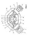
Figure 2 shows the junction box from the bottom side. Here it can be seen that thebottom wall 14 is designed asflange 19 that extends over the whole length of thesidewalls flange 19 is arranged such that it does not extend into theinterior space 10. Hence abottom opening 15 is provided which is limited by thesidewalls bottom opening 15 is closed by a surface of the solar panel. Preferably theflange 19 is glued to the surface of a solar panel by means of hot melt adhesive, such as a dow coming HM2500, which is a reactive hot melt neutral cure adhesive. - The junction box according to the present invention will be placed on a surface of a solar panel. Preferably the junction box is affixed to said surface by means of an adhesive. Afterwards the solder elements will be connected to the solder zones of a solar cell. After that the junction box according to the present invention is mechanically and electrically connected to a solar panel and the
interior space 10 will be filled with a filling material, such as a pottant or potting material. The filling material can also be a foam. Said filling material is insertable through theopening 16 that is arranged in thetop wall 13. Due to the fill in of the filling material the electrical contacts will be covered by the foam so that oxidation is prevented. Furthermore the filling material may have flame retardant properties. Theopening 16 receivesparts lid 2, as they are described by means offigure 5 . Theopening 16 is located such in the top wall that, when the lid is not present, access to saidelectrical contact elements 7 is provided. Preferably said access is provided in a substantially perpendicular or orthogonal direction to the surface of a solar panel. This means that a robot in a production line is able to quickly contact theelectrical contact elements 7 to corresponding contact zones of a solar panel. Reference is made tofigure 9d where this situation is clearly visible. Due to the specific shape of theopening 16 that provides access preferably to theelectrical contact elements 7 only, the other elements that are arranged in theinterior space 10 are protected by the remaining parts of thetop wall 15. Theopening 16 in thetop wall 15 is preferably designed as small as possible in order to allow access to theelectrical contact elements 7 only. This means that the remaining parts of thetop wall 15 are as large as possible. - Preferably the pottant or filling material is a silicone rubber such as an RTV pottant. A memontive (GE) TSE3664 condensation-cure flame retardant RTV can be used. TSE 3664 is a two-component condensation cure silicone rubber (RTV).
- In further embodiments it may also be possible that the
flange 19 extends from thesidewalls interior space 10 as well as in the direction to the external side. In such an embodiment thebottom opening 15 is limited by theflange 19. However, the surface of the solar panel still limits theinterior space 10 in the area of thebottom opening 15. - Alternatively it is also possible that the
flange 19 orbottom wall 14 extends from thesidewalls interior space 10 only. Also in that embodiment thebottom wall 14 comprises abottom opening 15 through which thesolder tail 7 extend to the external side. As mentioned in the above mentioned designs, the surface of the solar panel still limits theinterior space 10 in the area of thebottom opening 15. - As it can be seen in
figure 2 thefirst contact element 5 and thesecond contact element 6 extend through thesidewalls interior space 10 of the housing 1. Bothcontact elements internal contact element 7. Theinternal contact element 7 is preferably a solder tail which is described by means offigure 7 . Additionally thefirst contact element 5 is connected to thesecond contact element 7 by means of adiode 8. Theopening 16 is designed such that the diode can be arranged such that it is protected by the remaining parts of thetop wall 13. This means that thediode 8 is preferably not visible from the exterior when viewed in a direction perpendicular from thetop wall 13. However, in other embodiments thediode 8 is arranged such that it is at least partly visible from the exterior when viewed in a direction perpendicular from thetop wall 13. Such an arrangement is advantageous for quality checks. - Such a diode acts as a security device for bypass protection. Preferably a silicon diode rated 1000V/10A is used.
-
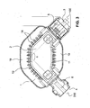
Figure 3 shows a top view of the junction box according to the present invention. This figure is mainly used to explain the angular arrangement of thefirst coupling 3 and thesecond coupling 4. Afirst axis 100 runs through thefirst coupling element 3 with thefirst contact element 5 and asecond axis 200 runs through thesecond coupling element 4 with thesecond contact element 6. If a plug is connected to said first orsecond coupling elements first axis 100 and thesecond axis 200 lie in the same plane, which plane is parallel to the surface of a solar panel or to thebottom surface 14 orflange 19, respectively. - As it can be seen in
figure 3 thefirst coupling element 3 and thesecond coupling element 4 are arranged angular with respect to each other. With other words, thefirst axis 100 is angular to thesecond axis 200. This is designated in the figure by means of an angle α. Preferably angle α is between 5° and 175°. However, other angles, larger than 175° or smaller than 5° are also possible. An angle α between 75° and 125° is particularly preferable, since the effect of the mechanical force that results from the cable (external connector) onto the couplings is minimized while the junction box is mounted. This is the case when the junction box is mounted such that the bisecting line of angle α is directed downwards, e.g. towards the roof of a building or the floor of a solar power plant etc. - Alternatively the plane in which the two
axis first coupling 3 and thesecond coupling 4 extend oblique with respect to thetop wall 13 or thebottom wall 14. This is a particular advantage if the solar panel is arranged tilted, since due to the oblique arrangement the couplings extend in a direction that is substantially perpendicular to the roof of building etc. -
Figure 4 shows a side view of the junction box according to the present invention. In this view one is able to see, that parts of the internal contact elements orsolder tails 7 extend over surface of theflange 19 orbottom wall 14. Hence said parts extend from theinterior space 10 over said surface to the external side or exterior space. If the junction box is mounted onto a solar panel, said parts will be connected to the solar cell, preferably via a soldered connection. Alternatively a welded or crimped connection is also thinkable. The solder tails extend with a measure D from the outer surface of thebottom wall 14. The measure D is preferably equal to or larger than the thickness of a glass pane of a solar panel, so that thesolder tails 7 are able to penetrate through a hole from one side of said glass pane to the other side of said glass pane. Preferably D is between 1 mm and 10 mm. In other embodiments D is between 3 mm to 5 mm. -
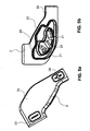
Figure 5a and 5b show thelid 2 from the front side (Figure 5a ) and from the back side (Figure 5b ).Said lid 2 has a shape that is substantially congruent with the surface of thetop wall 13. - On the
bottom surface 2a which faces thetop wall 13 of the housing 1 when being mounted thereto, the lid comprises afirst wall 20. Saidfirst wall 20 extends substantially perpendicular from thebottom surface 2a. Thewall 20 has a shape that is designed such that it fits around the outside of theopening 16 in thetop wall 13. Thewall 20 and thefirst sidewall 11 are designed such that there is a gap between thewall 20 and thefirst sidewall 11 of theopening 10. Said gap allows filling material to flow out as described hereinafter. In alternative embodiments thewall 20 is designed such that it fits into theopening 16 in thetop wall 13. Also in that embodiment thewall 20 and thefirst sidewall 11 are designed such that there is a gap between the two of them. In the present embodiment thewall 20 is designed as a closed loop. However, thewall 20 can also be designed as having several sections with interruptions. - Additionally the lid comprises
further embossments 21. Said embossments 21 extend also substantially perpendicular to thebottom surface 2a. Theembossments 21 are arranged within thewall 20. Preferably theembossments 21 have a larger height than thewall 20. - Also on the
bottom surface 2a there is arranged asecond wall 22 that surrounds thefirst wall 21. As thefirst wall 20 and theembossment 21 saidsecond wall 22 extends also perpendicular to thebottom surface 2a. - On the
top surface 2b of thelid 2 the lid comprisesindicators Such indicators respective coupling - Preferably the
lid 2 is made of plastics. Preferably polycarbonate, for example Lexan 940-701, is being used to provide the housing. Thelid 2 is preferably injection molded. -
Figures 6a and 6b show the junction box according to the present invention without thelid 2. As it can be seen thetop wall 13 comprises anopening 16. Theopening 16 is surrounded by aninner sidewall 171. Thisinner sidewall 171 extends preferably perpendicular from thetop wall 13. Furthermore theopening 16 is fully surrounded by theinner sidewall 171. Anouter sidewall 170 is arranged around the outer boundary of thetop wall 13. Preferably thetop wall 13 is fully surrounded by theouter sidewall 170. - The
top wall 13, theouter sidewall 170 and theinner sidewall 171 provide a space which can be designated asoverflow space 17. Before thelid 2 will be added to the housing 1, theinterior space 10 will be fully filled with filling material. As thelid 2 will be connected to the housing 1 some parts of the filling material will overflow from theinterior space 10 to theoverflow space 17 due to theembossments 21 and/or thefirst wall 20 that are arranged on theinner surface 2a of thelid 2. As there is a gap between thewall 22 of thelid 2 and thefirst sidewall 11 of theopening 10 filling material can flow through that gap as the lid is being pushed into position. Hence the filling material is forced to flow through theopening 16 in thetop wall 13 into theoverflow space 17. Since the filling material is forced to flow into theoverflow space 17, said filling material is present in theoverflow zone 17 as well as between theinner sidewall 171 and thefirst sidewall 20 of thelid 2. Therefore the filling material also acts as sealing means between thelid 2 and the housing 1. -
Figure 7a and 7b show thecontact elements internal contact elements 7 and thediode 8. The design of thecontact elements solder tail 7 is connected to thecontact elements - The internal contact element or
solder tail 7 comprises preferably acontact zone 71 through which thesolder tail 7 is connected to thefirst contact element 5 or thesecond contact element 6, respectively. A resilient zone 72 is arranged adjacent to thecontact zone 71. In the present embodiment the resilient zone 72 is shaped as an arc. Said arc or the resilient zone 72 can also be designated as bending structure, as the adjustment of the length of the solder element results in a bending motion in the arc. A transfer zone 73 links the resilient zone 72 to theactual solder zone 74. The resilient zone 72 is especially useful to adjust the distance D between thesolder zone 74 and the surface of the glass pane of a solar panel assembly in a resilient member. This allows a fully automatic manufacturing process. Thesolder zone 74 is connectable to the solar cell of a solar panel assembly. -
Figure 8a and 8b show thecontact elements internal contact elements 7 and thediode 8 arranged within thefirst coupling 3 and thesecond coupling 4. Preferably thecontact elements respective coupling -
Figure 9a - 9d illustrate a method for manufacturing a junction box according to the present invention. - The method for manufacturing a junction box according to the present invention comprises the steps of:
- providing the
first coupling 3 with afirst contact element 5 and thesecond coupling 4 with asecond contact element 6; (Fig. 9a ) - connecting the
first coupling 3 and thesecond coupling 4 with the housing 1 (Fig. 9d ). - providing each of the
contact elements solder tail 7; (Fig. 9b ) - affixing the
diode 8 at thefirst contact element 5 and at thesecond contact element 6; (Fig. 9c ) - The
first contact element 5 and thesecond contact element 6 are preferably contacted to thefirst coupling 3 and thesecond coupling 4 by means of an ultrasonic welding or a thermal insertion procedure. However, it is also possible to insert thecontact elements - The
solder tails 7 are preferably welded to the contact elements by means of an automatic resistance welding machine. The same applies to the diode. - The
first coupling 3 and thesecond coupling 4 are connected to the housing 1 means of an ultrasonic welding procedure. - The result is a pre-assembled junction box that is ready to be connected to a solar panel. These steps are designed to perform them on a fully automatic assembly line, so that the junction box according to present invention can be provided in a cost effective manner.
- A method for providing a solar panel with a junction box according to the present invention comprises the steps of :
- Applying adhesive to the junction box base perimeter or
flange 19; - affixing the junction box on a surface of a solar panel module;
- affixing solder tail to the contacts of a solar panel;
- filling the
interior space 10 of the housing with a filling material completely; and - mounting the lid 1 on the
top wall 13, so thatparts lid 2, extend into theinterior space 10 of the housing. - The junction box is affixed by means of an adhesive as it is described above.
- As it can be seen in
Figure 9d theopening 16 is arranged such that access to thesolder tails 7 is being provided through theopening 16. Access is provided in a direction substantially perpendicular to the surface of the solar panel. This means that parts of a robot in an assembly can enter into theinterior space 10 through theopening 16 in order to solder thesolder tails 7 to the solder zone of the solar cell. -
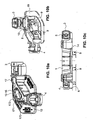
Figures 10a - 10c show a further embodiment of a junction box according to the present invention. It is noted that features of this embodiment can be combined with features of other embodiments and vice-versa to further embodiments. - The junction box 1 according to this embodiment comprises sidewalls 11, 12 that are designed stiff enough that the placement of ribs in order to stiffen the
sidewalls inner sidewall 171 that encompasses theopening 16 in thetop wall 13 comprises snap-inelements 172 for securing thelid 2. - Additionally by means of this embodiment a further embodiment of a solder tail is shown. Said solder tail is designated with
reference numeral 9. However, it has to be noted that such asolder tail 9 which may also be designated as solder element or solder tag can be used not only with the junction box as described herein, but with every other electrical device. The same applies to thesolder tail 7 as it is described above. -
Figure 10b and 10c show that thesolder tail 9 is arranged in the same manner as in the previous embodiment. Parts of thesolder tails 9 extend by a protruding height having a measure D from the outer surface of thebottom wall 14. The measure D is preferably equal to or larger than the thickness of a glass pane of a solar panel, so that thesolder tails 9 are able to penetrate through a hole from one side of said glass pane to the other side of said glass pane. Preferably D is between 1 mm and 10 mm. In other embodiments D is between 3 mm to 5 mm. -
Figures 11a to 11b show thesolder element 9 which is not part of the invention in a perspective view. Thesolder element 9 preferably comprises acontact zone 91, aresilient zone 92, atransfer zone 93 and asolder zone 94. Thesolder element 9 comprises a middle axis A along which the length of thesolder element 9 is adjustable. The length is considered to be the distance between thecontact zone 91 and thesolder zone 94. - The
contact zone 91 is provided to establish an electrical contact with a first electrical device (e.g. thefirst contact element 5 or second contact element 6). Preferably thecontact zone 91 is designed such that it may be connected to the electrical device by means of a solder connection, welded connection or a crimped connection etc.. In the present example thecontact zone 91 is formed as tubular body 910. Said tubular body 910 comprises a first end having several cutouts 911 and alid portion 912 and a second end on which theresilient zone 92 is formed. However, thecontact zone 91 can also be designated as being cylindrical. The term cylindrical is to be understood as having a circular, rectangular, oval, triangular or elliptical shaped as viewed along axis A. Furthermore it is possible that thecontact zone 91 is formed as a cylinder as defined above and that said cylinder is partly interrupted, preferably along the longitudinal axis. The interruption results in a gap in the cylindrical body. It is also possible that instead of the interruption the parts of the cylindrical or tubular body overlap each other. The lid portion is welded to theconnectors connectors solder element 9 or the solar panel, respectively. - The resilient zone or
compliant zone 92 comprises at least one, here four, resilient orcompliant webs 920. Theresilient webs 920 are designed such that they are deformable in order to adjust the length of thesolder element 9, i.e. the distance between thecontact zone 91 and thesolder zone 94. Said resilient webs are also designed as a bending structure, as the adjustment of the length of thesolder element 9 results in a bending motion to parts of theweb 920. In the present example theresilient webs 920 comprises anupper section 921 and alower section 922. Theupper section 921 is connected to the tubular body 910 and extends angular with respect to the middle axis A. In the present example theupper section 921 extends such that the distance between the middle axis A and theweb 920 increases with increasing length of theupper section 921. Thelower section 922 is connected to theupper section 921 and extends contrary to theupper section 921. This means for the present example that the distance between middle axis A and theweb 920 decreases with increasing length of thelower section 922. This leads to a structure in which thewebs 920 extends over a virtual circumference that is defined by the tubular body if viewed along the axis A. - In other examples of a solder element or
solder tail 9 it is also possible to provide aresilient zone 92 having a different structure. For example it is possible that theupper section 921 is arranged such that the distance between theupper section 921 and the axis A decreases with increasing length of theweb 920. This means that the web extends into the interior of that virtual circumference that is defined by the tubular body. - The
webs 920 of theresilient zone 92 are connected to thetransfer zone 93 which is also designed as atubular body 931. Preferably thetransfer zone 93 has the same diameter as thecontact zone 91. However, the diameter can also be larger or smaller than the diameter of thecontact zone 91. However, thetransfer zone 93 can also be designated as being cylindrical. The term cylindrical is to be understood as having a circular, rectangular, oval, triangular or elliptical shaped as viewed along axis A. Thetransfer zone 93 that is formed as a cylinder as defined above may be partly interrupted, preferably along the longitudinal axis. The interruption results in a gap in the cylindrical body. It is also possible that instead of the interruption the parts of the cylindrical or tubular body overlap each other. - The
solder zone 94 is provided to establish an electrical contact with a second electrical device (e.g. a solar panel). Saidsolder zone 94 extends from thetransfer zone 93. In the present example there is onesolder zone 94 arranged but in other examples it is also possible to arranged more than onesolder zone 94. Thesolder zone 94 here extends angular from the tubular body of thetransfer zone 93. -
Figure 11c shows thesolder element 9 not part of the present invention in a normal non-compressed state, whereasFigure 11d shows thesolder element 9 in a compressed state. The length of thesolder element 9 in the normal non-compressed state is designated with L1. The elongation of thesolder element 9 can be positive or negative. Positive elongation results in a length that is larger than length L1, whereas negative elongation results in a length that is shorter than length L1. Negative elongation is shown inFigure 11d , whereas the length of thesolder element 9 is designated with L2. Due to the design of thecompliant section 92, thesolder element 9 does not return from a compressed state into the non-compressed state as soon as the force F disappears. However, in other examples where thecompliant section 92 is resilient thesolder element 9 does return from a compressed state into the non-compressed state. - Preferably the
solder element 9 is made of copper, which allows compliant and permanent deformation. In other embodiments brass, bronze or aluminium may also be used. - Usually the force F is built up during a mounting process. To give an example: If the
solder element 9 not part of present invention is used in a junction box to provide a connection between photovoltaic solar panels, the force F is provided by a mounting tool which crushes thesolder element 9. The length L2 of the solder element after that is such that thesolder section 94 can be connected to the solar panel. -
Figure 12a and 12b show aweather cover 120 which can also be designated as a junction box having alid 121 and abase plate 124. The features of this embodiment can be combined with the features of the embodiment as disclosed herein. Thebase plate 124 provides an interior space forconnector strips 123 which are connected to a solar panel (not shown) on the one hand and to acable 125 via strain relieves 122 on the other hand. Thebase plate 124 comprises a flat bottom surface to be connected to a solar panel by means of an adhesive or a tape. Preferably thelid 121 and thebase plate 124 are made of a rigid polymeric material. - The
lid 121 is to be arranged onto thebase plate 124. Preferably thelid 121 is connected to thebase plate 124 via a snap-fit. For the reason thelid 121 and thebase plate 124 comprises protrusion which provide the snap-fit. The snap-fit also provides a sealed connection between thebase plate 124 and thelid 121. Furthermore it is possible to fill in the interior space with a filling material as disclosed above. - With such an assembly according to
figure 12a und 12b it is possible to provide a weather cover for connecting a first solar panel with a second solar panel. -
- 1
- housing
- 2
- lid
- 3
- first coupling
- 4
- second coupling
- 5
- first contact element
- 6
- second contact element
- 7
- solder tail
- 8
- diode
- 9
- solder tail, solder element
- 10
- interior space
- 11
- first sidewall
- 12
- second sidewall
- 13
- top wall
- 14
- bottom wall
- 15
- bottom opening
- 16
- opening
- 17
- overflow space
- 18
- ribs
- 19
- flange
- 20
- first wall
- 21
- embossments
- 22
- second wall
- 71
- contact zone
- 72
- resilient zone
- 73
- transfer zone
- 74
- solder zone
- 91
- contact zone
- 92
- resilient zone, compliant zone
- 93
- transfer zone
- 94
- solder zone
- 120
- weather cover
- 121
- lid
- 122
- strain relieves
- 123
- connector strips
- 124
- baseplate
- 125
- cable
- 170
- outer sidewall
- 171
- inner sidewall
- 172
- snap-in elements
- 910
- tubular body
- 911
- cut out
- 912
- lid
- 920
- compliant web
- 921
- upper section
- 922
- lower section
Claims (14)
- Junction box for a solar panel comprising a housing (1), a lid (2), a first coupling (3) and a second coupling (4), wherein the housing (1) comprises sidewalls (11, 12) and a top wall (13) defining an interior space (10), wherein the first coupling (3) comprises a first contact element (5) and the second coupling (4) comprises a second contact element (6), which contact elements (5, 6) penetrate at least one of the sidewalls (11, 12), so that the contact elements (5, 6) provide an electrical contact from external contact elements to internal contact elements, such as solder tails (7), which internal contact elements (7) are arranged at least partially in said interior space (10), wherein the top wall (13) comprises an opening (16) extending only partially in said top wall (13), said opening located in said top wall (13) such that access to said internal contact elements, such as said solder tails (7), in a perpendicular direction to the surface of a solar panel for connecting the internal contact elements, such as said solder tails (7), to the solar panel is provided,
characterized in that the first coupling (3) extends along a first axis (100) and the second coupling (4) extends along a second axis (200), wherein a first external contact element is introducible into the first coupling (3) along the first axis (100) and a second external contact element is introducible into the second coupling (4) along the second axis (200) and wherein the first axis (100) and the second axis (200) are arranged such that they are angular with an angle α that is between 5° and 170°, in particular between 75° and 125°, in a common plane that is preferably parallel to the bottom wall (14). - Junction box according to claim 1, characterized in that the first coupling (3) and the second coupling (4) are connected to sidewalls (11, 12), wherein the sidewalls (11, 12) comprise holes in order to allow the contact element (5) to extend into the interior space (10).
- Junction box according to any of the preceding claims, characterized in that the top wall (13) comprises an outer sidewall (170) that extends perpendicular from the top wall (13) and that surrounds the outer circumference of the top wall (13), so that an overflow space (17) is defined by the top wall (13) and the outer sidewall (170).
- Junction box according to any of the preceding claims, characterized in that the opening (16) is surrounded by an inner sidewall (171) which extends perpendicular from said top wall (13).
- Junction box according to any of the preceding claims, characterized in that a filling material is injectable into the interior space (10) through said opening (16), so that the interior space (10) is fully filled with said filling material, and in that the opening (16) is closeable with the lid (2).
- Junction box according to any of the preceding claims, characterized in that the lid (2) comprises a wall (20) extending perpendicular to the lid (2) and having a shape that fits into or around the opening (16) in the top surface.
- Junction box according to any of the preceding claims, characterized in that the lid (2) comprises further embossments (21) that are arranged such that they extend through the opening (16) into the interior space (10) when said lid being mounted onto the housing (1), wherein due to said further embossments (21) filling material is forced to flow through the opening (16) into the overflow space (17), when said lid (2) is mounted onto the housing (1) filled with the filling material.
- Junction box according any of the preceding claims, characterized in that parts of the solder tail (7) extend from the interior space (10) through a bottom opening (15) in the bottom wall (14) over the surface of the bottom wall (14).
- Junction box according to claim 8, characterized in that the solder tail (7, 9) comprises a resilient section (72, 92), so that the parts of the solder tail (7, 9) that extend over the bottom side (14) are moveable with respect to the bottom side (14).
- Junction box according to any of the preceding claims, characterized in that the contact element (5) of the first coupling (3) is connected with a diode (8) to the contact element (6) of the second coupling (4), wherein the diode (8) is arranged such that the diode (8) is covered by parts of the top wall (13).
- Method for manufacturing a junction box according to one of the claims 1 to 10, characterized in that the method comprises the steps of- providing the first coupling (3) with a first contact element (5) and the second coupling (4) with a second contact (6) element;- connecting the first coupling (3) and the second coupling (4) with the housing (1);- providing each of the contact elements (5, 6) with a solder tail (7, 9);- affixing the diode (8) at the first contact element (5) and at the second contact element (6).
- Method for providing a solar panel with a junction box according to one of the claims 1 to 10, characterized in that the method comprises the steps of:- applying adhesive to the junction box base perimeter or flange;- arranging the junction box on a surface of a solar panel module;- affixing solder tail to the contacts of a solar panel, preferably in perpendicular direction;- filling the interior space (10) of the housing with a filling material, preferably completely; and- mounting the lid (1) on the top wall, so that parts (20, 21) of the lid, extend into the interior space (10) of the housing.
- Photovoltaic solar panel comprising at least a carrier layer and a solar cell that is arranged on the front side of said carrier layer, wherein a junction box according any of claims 1 to 10, is arranged on the back side of said carrier layer.
- Photovoltaic solar panel according to claim 13, characterized in that the bottom side (14) the junction box faces the back side of said carrier layer and in that the carrier layer comprises openings through which the solder elements (7) are passed through to the solar cell.
Priority Applications (1)
| Application Number | Priority Date | Filing Date | Title |
|---|---|---|---|
| EP13170289.6A EP2637219B1 (en) | 2007-11-12 | 2008-10-30 | Junction box for a photovoltaic solar panel |
Applications Claiming Priority (4)
| Application Number | Priority Date | Filing Date | Title |
|---|---|---|---|
| US98722907P | 2007-11-12 | 2007-11-12 | |
| EP08405011A EP2058867A3 (en) | 2007-11-12 | 2008-01-16 | Junction box for a photovoltaic solar panel |
| EP13170289.6A EP2637219B1 (en) | 2007-11-12 | 2008-10-30 | Junction box for a photovoltaic solar panel |
| EP08849190.7A EP2210281B1 (en) | 2007-11-12 | 2008-10-30 | Junction box for a photovoltaic solar panel |
Related Parent Applications (2)
| Application Number | Title | Priority Date | Filing Date |
|---|---|---|---|
| EP08849190.7A Division EP2210281B1 (en) | 2007-11-12 | 2008-10-30 | Junction box for a photovoltaic solar panel |
| EP08849190.7 Division | 2008-10-30 |
Publications (3)
| Publication Number | Publication Date |
|---|---|
| EP2637219A2 EP2637219A2 (en) | 2013-09-11 |
| EP2637219A3 EP2637219A3 (en) | 2014-01-15 |
| EP2637219B1 true EP2637219B1 (en) | 2015-07-08 |
Family
ID=40386437
Family Applications (4)
| Application Number | Title | Priority Date | Filing Date |
|---|---|---|---|
| EP08405011A Withdrawn EP2058867A3 (en) | 2007-11-12 | 2008-01-16 | Junction box for a photovoltaic solar panel |
| EP13170286.2A Withdrawn EP2637218A1 (en) | 2007-11-12 | 2008-10-30 | Solder element for a junction box and method for producing a solder element |
| EP08849190.7A Not-in-force EP2210281B1 (en) | 2007-11-12 | 2008-10-30 | Junction box for a photovoltaic solar panel |
| EP13170289.6A Not-in-force EP2637219B1 (en) | 2007-11-12 | 2008-10-30 | Junction box for a photovoltaic solar panel |
Family Applications Before (3)
| Application Number | Title | Priority Date | Filing Date |
|---|---|---|---|
| EP08405011A Withdrawn EP2058867A3 (en) | 2007-11-12 | 2008-01-16 | Junction box for a photovoltaic solar panel |
| EP13170286.2A Withdrawn EP2637218A1 (en) | 2007-11-12 | 2008-10-30 | Solder element for a junction box and method for producing a solder element |
| EP08849190.7A Not-in-force EP2210281B1 (en) | 2007-11-12 | 2008-10-30 | Junction box for a photovoltaic solar panel |
Country Status (7)
| Country | Link |
|---|---|
| US (2) | US8500462B2 (en) |
| EP (4) | EP2058867A3 (en) |
| JP (3) | JP5395802B2 (en) |
| CN (1) | CN101855732B (en) |
| ES (1) | ES2428885T3 (en) |
| TW (1) | TWI453937B (en) |
| WO (1) | WO2009062326A2 (en) |
Families Citing this family (44)
| Publication number | Priority date | Publication date | Assignee | Title |
|---|---|---|---|---|
| EP2058867A3 (en) * | 2007-11-12 | 2009-07-22 | Multi-Holding AG | Junction box for a photovoltaic solar panel |
| US7824189B1 (en) | 2009-04-15 | 2010-11-02 | Tyco Electronics Corporation | Junction box for photovoltaic modules |
| US8690110B2 (en) * | 2009-05-25 | 2014-04-08 | Solaredge Technologies Ltd. | Bracket for connection of a junction box to photovoltaic panels |
| EP2256825B1 (en) * | 2009-05-27 | 2017-09-06 | Yamaichi Electronics Deutschland GmbH | Connection or bridging socket with soldering agent reservoir |
| DE102009040568A1 (en) * | 2009-09-08 | 2011-03-24 | Yamaichi Electronics Deutschland Gmbh | Junction box, use, solar panel and procedure |
| CN102498658B (en) * | 2009-09-11 | 2015-02-18 | 第一太阳能有限公司 | Cord plate |
| DE102009041968A1 (en) * | 2009-09-21 | 2011-04-07 | Telegärtner Gerätebau GmbH | Junction box arrangement for the electrical connection of a solar module |
| CN102035157B (en) * | 2009-09-25 | 2013-02-27 | 无锡尚德太阳能电力有限公司 | Junction box for solar cell module and solar cell module |
| US20110155456A1 (en) * | 2009-12-29 | 2011-06-30 | Du Pont Apollo Limited | Junction box for solar panel |
| CN102195522B (en) * | 2010-03-15 | 2014-12-17 | 泰科电子(上海)有限公司 | Wiring module for BIPV (building integrated photovoltaic) system |
| DE202010005210U1 (en) * | 2010-04-15 | 2010-07-29 | Kumatec Sondermaschinenbau & Kunststoffverarbeitung Gmbh | photovoltaic module |
| CN103026501B (en) * | 2010-06-30 | 2015-09-02 | 第一太阳能有限公司 | For the moisture resistant cord plate of photovoltaic module |
| DE102010034634B3 (en) * | 2010-08-17 | 2011-12-08 | Lumberg Connect Gmbh | Junction box with holding device for connectors |
| DE102010044872B4 (en) * | 2010-09-09 | 2014-06-05 | Lumberg Connect Gmbh | Connection box for solar module |
| FR2965290B1 (en) * | 2010-09-28 | 2012-10-12 | Dickson Constant | STORE-TYPE SOLAR PROTECTION DEVICE WITH A SYSTEM FOR GENERATING ELECTRICAL ENERGY |
| US9287648B2 (en) | 2010-12-09 | 2016-03-15 | Multi-Holding Ag | Contact element, in particular a solder tab and photovoltaic junction box with contact element, in particular a solder tab |
| DE102011009005B4 (en) * | 2011-01-14 | 2014-07-31 | Solon Se | Electrical junction box for a photovoltaic module |
| CH704385A1 (en) | 2011-01-26 | 2012-07-31 | Multi Holding Ag | Outlets housing for photovoltaic junction boxes. |
| CH704449A1 (en) | 2011-02-03 | 2012-08-15 | Multi Holding Ag | A photovoltaic solar module with a junction box. |
| JP5605909B2 (en) * | 2011-02-23 | 2014-10-15 | ホシデン株式会社 | Solar cell module terminal and solar cell module terminal box |
| CN102738619A (en) * | 2011-04-14 | 2012-10-17 | 乐清市信达利实业有限公司 | Conductive plate |
| CN102769052A (en) * | 2011-04-14 | 2012-11-07 | 乐清市信达利实业有限公司 | Junction box with cable connector |
| CN202103381U (en) * | 2011-04-14 | 2012-01-04 | 乐清市信达利实业有限公司 | Junction box shell |
| CN102738276B (en) * | 2011-04-14 | 2015-08-05 | 乐清市信达利实业有限公司 | Terminal box |
| GB2490499A (en) | 2011-05-03 | 2012-11-07 | Solaredge Technologies Ltd | Junction box assembly for electrical connections to photovoltaic panels |
| JP5729648B2 (en) * | 2011-10-13 | 2015-06-03 | ホシデン株式会社 | Terminal box for solar cell module |
| JP5790940B2 (en) | 2011-12-19 | 2015-10-07 | ホシデン株式会社 | Terminal box |
| US9331631B2 (en) | 2012-08-31 | 2016-05-03 | First Solar, Inc. | Direct connection of lead bar to conductive ribbon in a thin film photovoltaic device |
| EP2917976A1 (en) * | 2012-11-12 | 2015-09-16 | Multi-Holding AG | Plug housing and socket housing for plug connectors |
| US9685568B2 (en) * | 2014-03-12 | 2017-06-20 | Merlin Solar Technologies, Inc. | Photovoltaic module with flexible circuit |
| EP2860765A1 (en) | 2013-10-11 | 2015-04-15 | Multi-Holding AG | Junction box, and method for mounting a junction box |
| JP6366926B2 (en) | 2013-11-11 | 2018-08-01 | 株式会社ミツトヨ | Industrial machine and method for measuring the amount of expansion and contraction |
| US20150249426A1 (en) * | 2014-02-28 | 2015-09-03 | David Okawa | Photovoltaic module junction box |
| JP2017524326A (en) * | 2014-07-25 | 2017-08-24 | マルチ−ホールディング アーゲー | Junction box for solar cell module |
| TWM507611U (en) * | 2015-02-17 | 2015-08-21 | Switchlab Inc | Clip-on contact box structure |
| US10256769B2 (en) * | 2015-06-29 | 2019-04-09 | Te Connectivity Corporation | Terminal for solar junction box |
| US9780723B2 (en) * | 2015-06-29 | 2017-10-03 | Te Connectivity Corporation | Terminal for solar junction box |
| CN205336219U (en) * | 2015-12-08 | 2016-06-22 | 泰科电子(上海)有限公司 | Photovoltaic terminal box and diode |
| CN113676133B (en) * | 2016-02-29 | 2024-08-09 | 韩华新能源(德国)有限责任公司 | Covering element for a junction box of a solar module |
| DE102017118267A1 (en) * | 2017-08-10 | 2019-02-14 | Hanwha Q Cells Gmbh | Junction box for a photovoltaic module |
| US11095248B2 (en) | 2017-11-30 | 2021-08-17 | TE Connectivity Services Gmbh | Solar junction box |
| US20200382052A1 (en) * | 2019-05-29 | 2020-12-03 | Solarwindow Technologies, Inc | Homogeneous transparent coated greenhouse electrical generating devices, and internal and external electrical interconnections |
| CN116670954A (en) * | 2020-12-15 | 2023-08-29 | 伊顿智能动力有限公司 | U-shaped lead box |
| US11990713B2 (en) * | 2021-10-25 | 2024-05-21 | Nvidia Corporation | Connector positioning system and method |
Family Cites Families (21)
| Publication number | Priority date | Publication date | Assignee | Title |
|---|---|---|---|---|
| US4654470A (en) * | 1983-10-31 | 1987-03-31 | Amp Incorporated | Raintight junction box |
| US5184692A (en) * | 1991-03-18 | 1993-02-09 | Schlumberger Technology Corporation | Retrievable radiation source carrier |
| JP3779346B2 (en) | 1995-01-20 | 2006-05-24 | 日本発条株式会社 | LSI package socket |
| US6046597A (en) * | 1995-10-04 | 2000-04-04 | Oz Technologies, Inc. | Test socket for an IC device |
| US20020018344A1 (en) * | 1996-03-08 | 2002-02-14 | Thomas & Betts International | Overhead luminaire |
| JPH1126035A (en) * | 1997-07-04 | 1999-01-29 | Engel Kogyo Kk | Terminal box for solar cell module |
| JP4025885B2 (en) * | 1998-02-06 | 2007-12-26 | 協伸工業株式会社 | Connector chip and taping connector chip |
| US5980335A (en) * | 1998-03-27 | 1999-11-09 | Molex Incorporated | Electrical terminal |
| JP2001098856A (en) * | 1999-09-30 | 2001-04-10 | Matsushita Seiko Co Ltd | Double glazing |
| JP2001168368A (en) * | 1999-12-09 | 2001-06-22 | Kanegafuchi Chem Ind Co Ltd | Terminal box |
| US6392524B1 (en) * | 2000-06-09 | 2002-05-21 | Xerox Corporation | Photolithographically-patterned out-of-plane coil structures and method of making |
| US6543940B2 (en) * | 2001-04-05 | 2003-04-08 | Max Chu | Fiber converter faceplate outlet |
| US6720511B2 (en) | 2002-09-05 | 2004-04-13 | Litton Systems, Inc. | One-piece semi-rigid electrical contact |
| DE20311183U1 (en) * | 2003-07-21 | 2004-07-08 | Tyco Electronics Amp Gmbh | Junction box for a solar panel and solar panel |
| JP2005050867A (en) | 2003-07-29 | 2005-02-24 | Kyocera Corp | Solar cell module |
| US7347698B2 (en) * | 2004-03-19 | 2008-03-25 | Neoconix, Inc. | Deep drawn electrical contacts and method for making |
| JP3904114B2 (en) * | 2004-04-23 | 2007-04-11 | 住友電装株式会社 | Manufacturing method of terminal box for solar cell module |
| US7880080B2 (en) * | 2005-02-11 | 2011-02-01 | Bp Corporation North America Inc. | Junction box for output wiring from solar module and method of installing same |
| US7109416B1 (en) * | 2005-11-21 | 2006-09-19 | Norman Reed | Electrical wiring access box |
| US7291036B1 (en) * | 2006-11-08 | 2007-11-06 | Tyco Electronics Corporation | Photovoltaic connection system |
| EP2058867A3 (en) * | 2007-11-12 | 2009-07-22 | Multi-Holding AG | Junction box for a photovoltaic solar panel |
-
2008
- 2008-01-16 EP EP08405011A patent/EP2058867A3/en not_active Withdrawn
- 2008-10-30 US US12/742,554 patent/US8500462B2/en not_active Expired - Fee Related
- 2008-10-30 EP EP13170286.2A patent/EP2637218A1/en not_active Withdrawn
- 2008-10-30 JP JP2010533405A patent/JP5395802B2/en not_active Expired - Fee Related
- 2008-10-30 WO PCT/CH2008/000455 patent/WO2009062326A2/en not_active Ceased
- 2008-10-30 EP EP08849190.7A patent/EP2210281B1/en not_active Not-in-force
- 2008-10-30 CN CN2008801157671A patent/CN101855732B/en not_active Expired - Fee Related
- 2008-10-30 ES ES08849190T patent/ES2428885T3/en active Active
- 2008-10-30 EP EP13170289.6A patent/EP2637219B1/en not_active Not-in-force
- 2008-11-11 TW TW097143484A patent/TWI453937B/en not_active IP Right Cessation
-
2013
- 2013-06-11 US US13/915,188 patent/US9059350B2/en not_active Expired - Fee Related
- 2013-07-09 JP JP2013144053A patent/JP2013232675A/en active Pending
- 2013-07-09 JP JP2013144054A patent/JP5694454B2/en not_active Expired - Fee Related
Also Published As
| Publication number | Publication date |
|---|---|
| ES2428885T3 (en) | 2013-11-12 |
| EP2637219A2 (en) | 2013-09-11 |
| EP2058867A3 (en) | 2009-07-22 |
| JP5694454B2 (en) | 2015-04-01 |
| JP5395802B2 (en) | 2014-01-22 |
| WO2009062326A2 (en) | 2009-05-22 |
| CN101855732B (en) | 2012-06-20 |
| JP2013232675A (en) | 2013-11-14 |
| EP2637219A3 (en) | 2014-01-15 |
| US9059350B2 (en) | 2015-06-16 |
| EP2210281A2 (en) | 2010-07-28 |
| TWI453937B (en) | 2014-09-21 |
| EP2637218A1 (en) | 2013-09-11 |
| JP2013258149A (en) | 2013-12-26 |
| US20120060919A1 (en) | 2012-03-15 |
| EP2058867A2 (en) | 2009-05-13 |
| EP2210281B1 (en) | 2013-07-17 |
| US20130276856A1 (en) | 2013-10-24 |
| WO2009062326A3 (en) | 2009-07-09 |
| CN101855732A (en) | 2010-10-06 |
| TW200931673A (en) | 2009-07-16 |
| US8500462B2 (en) | 2013-08-06 |
| JP2011503884A (en) | 2011-01-27 |
Similar Documents
| Publication | Publication Date | Title |
|---|---|---|
| EP2210281B1 (en) | Junction box for a photovoltaic solar panel | |
| US7862383B2 (en) | Electrical connector for a solar module assembly | |
| US7938661B2 (en) | Photovoltaic module connector assembly | |
| US20050022859A1 (en) | Connector for a solar module | |
| US20110183531A1 (en) | Junction box for photovoltaic modules | |
| KR20070110330A (en) | Junction box for output wiring of solar cell module and installation method | |
| EP3314747B1 (en) | Solar junction box | |
| EP1102354B1 (en) | Apparatus for contacting foil conductors, in particular of a solar module | |
| US10256769B2 (en) | Terminal for solar junction box | |
| CN105378941B (en) | Connector system for photovoltaic arrays | |
| US20160301362A1 (en) | Housing for Solar Panel Electric Connection | |
| JP2012028407A (en) | Potting liquid leakage prevention structure of terminal box | |
| EP2450962B1 (en) | Terminal box for solar cell modules, and solar cell module using same | |
| JP5608002B2 (en) | Terminal box | |
| KR101155927B1 (en) | Junction box for building-integrated photovoltaic modules | |
| EP4472066A1 (en) | Frame-attached junction box for solar cell modules | |
| US20260001208A1 (en) | Tool having a sealing pocket for an electrical component | |
| WO2024022974A1 (en) | Connector for photovoltaic panel in a vehicle | |
| US11095248B2 (en) | Solar junction box | |
| JP2025512535A (en) | Fluid Control Unit | |
| CN114287106A (en) | Electrical modular junction box transmission device (E-JBTD) system with internal and external electrical power connections |
Legal Events
| Date | Code | Title | Description |
|---|---|---|---|
| PUAI | Public reference made under article 153(3) epc to a published international application that has entered the european phase |
Free format text: ORIGINAL CODE: 0009012 |
|
| AC | Divisional application: reference to earlier application |
Ref document number: 2210281 Country of ref document: EP Kind code of ref document: P |
|
| AK | Designated contracting states |
Kind code of ref document: A2 Designated state(s): AT BE BG CH CY CZ DE DK EE ES FI FR GB GR HR HU IE IS IT LI LT LU LV MC MT NL NO PL PT RO SE SI SK TR |
|
| RIN1 | Information on inventor provided before grant (corrected) |
Inventor name: ELGAR, YACOV Inventor name: SULLIVAN, JEFFREY S. Inventor name: WEATHERLEY, IAN Inventor name: STREET, ROBERT D. Inventor name: MILLS, BRIAN WADE Inventor name: PRATT, IAN MCKAY Inventor name: LU, DANNY CAM TOAN Inventor name: CARVER, DUSTIN DELMAR REEDE |
|
| PUAL | Search report despatched |
Free format text: ORIGINAL CODE: 0009013 |
|
| AK | Designated contracting states |
Kind code of ref document: A3 Designated state(s): AT BE BG CH CY CZ DE DK EE ES FI FR GB GR HR HU IE IS IT LI LT LU LV MC MT NL NO PL PT RO SE SI SK TR |
|
| RIC1 | Information provided on ipc code assigned before grant |
Ipc: H01R 13/66 20060101ALI20131206BHEP Ipc: H01R 31/06 20060101ALN20131206BHEP Ipc: H01R 11/09 20060101ALN20131206BHEP Ipc: H01L 31/048 20060101AFI20131206BHEP |
|
| 17P | Request for examination filed |
Effective date: 20140509 |
|
| RBV | Designated contracting states (corrected) |
Designated state(s): AT BE BG CH CY CZ DE DK EE ES FI FR GB GR HR HU IE IS IT LI LT LU LV MC MT NL NO PL PT RO SE SI SK TR |
|
| GRAP | Despatch of communication of intention to grant a patent |
Free format text: ORIGINAL CODE: EPIDOSNIGR1 |
|
| RIC1 | Information provided on ipc code assigned before grant |
Ipc: H01L 31/048 20140101AFI20150107BHEP Ipc: H01R 13/66 20060101ALI20150107BHEP Ipc: H02S 40/34 20140101ALI20150107BHEP Ipc: H01R 11/09 20060101ALN20150107BHEP Ipc: H01R 31/06 20060101ALN20150107BHEP |
|
| RIC1 | Information provided on ipc code assigned before grant |
Ipc: H01R 13/66 20060101ALI20150114BHEP Ipc: H01R 31/06 20060101ALN20150114BHEP Ipc: H01L 31/048 20140101AFI20150114BHEP Ipc: H02S 40/34 20140101ALI20150114BHEP Ipc: H01R 11/09 20060101ALN20150114BHEP |
|
| INTG | Intention to grant announced |
Effective date: 20150128 |
|
| GRAS | Grant fee paid |
Free format text: ORIGINAL CODE: EPIDOSNIGR3 |
|
| GRAA | (expected) grant |
Free format text: ORIGINAL CODE: 0009210 |
|
| AC | Divisional application: reference to earlier application |
Ref document number: 2210281 Country of ref document: EP Kind code of ref document: P |
|
| AK | Designated contracting states |
Kind code of ref document: B1 Designated state(s): AT BE BG CH CY CZ DE DK EE ES FI FR GB GR HR HU IE IS IT LI LT LU LV MC MT NL NO PL PT RO SE SI SK TR |
|
| REG | Reference to a national code |
Ref country code: GB Ref legal event code: FG4D |
|
| REG | Reference to a national code |
Ref country code: AT Ref legal event code: REF Ref document number: 735982 Country of ref document: AT Kind code of ref document: T Effective date: 20150715 Ref country code: CH Ref legal event code: EP Ref country code: CH Ref legal event code: NV Representative=s name: ISLER AND PEDRAZZINI AG, CH |
|
| REG | Reference to a national code |
Ref country code: IE Ref legal event code: FG4D |
|
| REG | Reference to a national code |
Ref country code: DE Ref legal event code: R096 Ref document number: 602008038996 Country of ref document: DE |
|
| REG | Reference to a national code |
Ref country code: FR Ref legal event code: PLFP Year of fee payment: 8 |
|
| REG | Reference to a national code |
Ref country code: AT Ref legal event code: MK05 Ref document number: 735982 Country of ref document: AT Kind code of ref document: T Effective date: 20150708 |
|
| REG | Reference to a national code |
Ref country code: NL Ref legal event code: MP Effective date: 20150708 |
|
| REG | Reference to a national code |
Ref country code: LT Ref legal event code: MG4D |
|
| PG25 | Lapsed in a contracting state [announced via postgrant information from national office to epo] |
Ref country code: GR Free format text: LAPSE BECAUSE OF FAILURE TO SUBMIT A TRANSLATION OF THE DESCRIPTION OR TO PAY THE FEE WITHIN THE PRESCRIBED TIME-LIMIT Effective date: 20151009 Ref country code: LT Free format text: LAPSE BECAUSE OF FAILURE TO SUBMIT A TRANSLATION OF THE DESCRIPTION OR TO PAY THE FEE WITHIN THE PRESCRIBED TIME-LIMIT Effective date: 20150708 Ref country code: LV Free format text: LAPSE BECAUSE OF FAILURE TO SUBMIT A TRANSLATION OF THE DESCRIPTION OR TO PAY THE FEE WITHIN THE PRESCRIBED TIME-LIMIT Effective date: 20150708 Ref country code: FI Free format text: LAPSE BECAUSE OF FAILURE TO SUBMIT A TRANSLATION OF THE DESCRIPTION OR TO PAY THE FEE WITHIN THE PRESCRIBED TIME-LIMIT Effective date: 20150708 Ref country code: NO Free format text: LAPSE BECAUSE OF FAILURE TO SUBMIT A TRANSLATION OF THE DESCRIPTION OR TO PAY THE FEE WITHIN THE PRESCRIBED TIME-LIMIT Effective date: 20151008 |
|
| PG25 | Lapsed in a contracting state [announced via postgrant information from national office to epo] |
Ref country code: SE Free format text: LAPSE BECAUSE OF FAILURE TO SUBMIT A TRANSLATION OF THE DESCRIPTION OR TO PAY THE FEE WITHIN THE PRESCRIBED TIME-LIMIT Effective date: 20150708 Ref country code: PT Free format text: LAPSE BECAUSE OF FAILURE TO SUBMIT A TRANSLATION OF THE DESCRIPTION OR TO PAY THE FEE WITHIN THE PRESCRIBED TIME-LIMIT Effective date: 20151109 Ref country code: IS Free format text: LAPSE BECAUSE OF FAILURE TO SUBMIT A TRANSLATION OF THE DESCRIPTION OR TO PAY THE FEE WITHIN THE PRESCRIBED TIME-LIMIT Effective date: 20151108 Ref country code: ES Free format text: LAPSE BECAUSE OF FAILURE TO SUBMIT A TRANSLATION OF THE DESCRIPTION OR TO PAY THE FEE WITHIN THE PRESCRIBED TIME-LIMIT Effective date: 20150708 Ref country code: HR Free format text: LAPSE BECAUSE OF FAILURE TO SUBMIT A TRANSLATION OF THE DESCRIPTION OR TO PAY THE FEE WITHIN THE PRESCRIBED TIME-LIMIT Effective date: 20150708 Ref country code: PL Free format text: LAPSE BECAUSE OF FAILURE TO SUBMIT A TRANSLATION OF THE DESCRIPTION OR TO PAY THE FEE WITHIN THE PRESCRIBED TIME-LIMIT Effective date: 20150708 Ref country code: AT Free format text: LAPSE BECAUSE OF FAILURE TO SUBMIT A TRANSLATION OF THE DESCRIPTION OR TO PAY THE FEE WITHIN THE PRESCRIBED TIME-LIMIT Effective date: 20150708 |
|
| REG | Reference to a national code |
Ref country code: DE Ref legal event code: R097 Ref document number: 602008038996 Country of ref document: DE |
|
| PG25 | Lapsed in a contracting state [announced via postgrant information from national office to epo] |
Ref country code: DK Free format text: LAPSE BECAUSE OF FAILURE TO SUBMIT A TRANSLATION OF THE DESCRIPTION OR TO PAY THE FEE WITHIN THE PRESCRIBED TIME-LIMIT Effective date: 20150708 Ref country code: EE Free format text: LAPSE BECAUSE OF FAILURE TO SUBMIT A TRANSLATION OF THE DESCRIPTION OR TO PAY THE FEE WITHIN THE PRESCRIBED TIME-LIMIT Effective date: 20150708 Ref country code: CZ Free format text: LAPSE BECAUSE OF FAILURE TO SUBMIT A TRANSLATION OF THE DESCRIPTION OR TO PAY THE FEE WITHIN THE PRESCRIBED TIME-LIMIT Effective date: 20150708 Ref country code: IT Free format text: LAPSE BECAUSE OF FAILURE TO SUBMIT A TRANSLATION OF THE DESCRIPTION OR TO PAY THE FEE WITHIN THE PRESCRIBED TIME-LIMIT Effective date: 20150708 Ref country code: SK Free format text: LAPSE BECAUSE OF FAILURE TO SUBMIT A TRANSLATION OF THE DESCRIPTION OR TO PAY THE FEE WITHIN THE PRESCRIBED TIME-LIMIT Effective date: 20150708 |
|
| PLBE | No opposition filed within time limit |
Free format text: ORIGINAL CODE: 0009261 |
|
| STAA | Information on the status of an ep patent application or granted ep patent |
Free format text: STATUS: NO OPPOSITION FILED WITHIN TIME LIMIT |
|
| PG25 | Lapsed in a contracting state [announced via postgrant information from national office to epo] |
Ref country code: LU Free format text: LAPSE BECAUSE OF FAILURE TO SUBMIT A TRANSLATION OF THE DESCRIPTION OR TO PAY THE FEE WITHIN THE PRESCRIBED TIME-LIMIT Effective date: 20151030 Ref country code: RO Free format text: LAPSE BECAUSE OF FAILURE TO SUBMIT A TRANSLATION OF THE DESCRIPTION OR TO PAY THE FEE WITHIN THE PRESCRIBED TIME-LIMIT Effective date: 20150708 |
|
| REG | Reference to a national code |
Ref country code: CH Ref legal event code: PL |
|
| 26N | No opposition filed |
Effective date: 20160411 |
|
| GBPC | Gb: european patent ceased through non-payment of renewal fee |
Effective date: 20151030 |
|
| PG25 | Lapsed in a contracting state [announced via postgrant information from national office to epo] |
Ref country code: MC Free format text: LAPSE BECAUSE OF FAILURE TO SUBMIT A TRANSLATION OF THE DESCRIPTION OR TO PAY THE FEE WITHIN THE PRESCRIBED TIME-LIMIT Effective date: 20150708 |
|
| REG | Reference to a national code |
Ref country code: IE Ref legal event code: MM4A |
|
| PG25 | Lapsed in a contracting state [announced via postgrant information from national office to epo] |
Ref country code: GB Free format text: LAPSE BECAUSE OF NON-PAYMENT OF DUE FEES Effective date: 20151030 Ref country code: CH Free format text: LAPSE BECAUSE OF NON-PAYMENT OF DUE FEES Effective date: 20151031 Ref country code: LI Free format text: LAPSE BECAUSE OF NON-PAYMENT OF DUE FEES Effective date: 20151031 |
|
| PG25 | Lapsed in a contracting state [announced via postgrant information from national office to epo] |
Ref country code: SI Free format text: LAPSE BECAUSE OF FAILURE TO SUBMIT A TRANSLATION OF THE DESCRIPTION OR TO PAY THE FEE WITHIN THE PRESCRIBED TIME-LIMIT Effective date: 20150708 |
|
| REG | Reference to a national code |
Ref country code: FR Ref legal event code: PLFP Year of fee payment: 9 |
|
| PG25 | Lapsed in a contracting state [announced via postgrant information from national office to epo] |
Ref country code: IE Free format text: LAPSE BECAUSE OF NON-PAYMENT OF DUE FEES Effective date: 20151030 |
|
| PG25 | Lapsed in a contracting state [announced via postgrant information from national office to epo] |
Ref country code: BE Free format text: LAPSE BECAUSE OF FAILURE TO SUBMIT A TRANSLATION OF THE DESCRIPTION OR TO PAY THE FEE WITHIN THE PRESCRIBED TIME-LIMIT Effective date: 20150708 |
|
| PG25 | Lapsed in a contracting state [announced via postgrant information from national office to epo] |
Ref country code: BG Free format text: LAPSE BECAUSE OF FAILURE TO SUBMIT A TRANSLATION OF THE DESCRIPTION OR TO PAY THE FEE WITHIN THE PRESCRIBED TIME-LIMIT Effective date: 20150708 Ref country code: HU Free format text: LAPSE BECAUSE OF FAILURE TO SUBMIT A TRANSLATION OF THE DESCRIPTION OR TO PAY THE FEE WITHIN THE PRESCRIBED TIME-LIMIT; INVALID AB INITIO Effective date: 20081030 |
|
| PG25 | Lapsed in a contracting state [announced via postgrant information from national office to epo] |
Ref country code: CY Free format text: LAPSE BECAUSE OF FAILURE TO SUBMIT A TRANSLATION OF THE DESCRIPTION OR TO PAY THE FEE WITHIN THE PRESCRIBED TIME-LIMIT Effective date: 20150708 Ref country code: NL Free format text: LAPSE BECAUSE OF FAILURE TO SUBMIT A TRANSLATION OF THE DESCRIPTION OR TO PAY THE FEE WITHIN THE PRESCRIBED TIME-LIMIT Effective date: 20150708 |
|
| PG25 | Lapsed in a contracting state [announced via postgrant information from national office to epo] |
Ref country code: MT Free format text: LAPSE BECAUSE OF FAILURE TO SUBMIT A TRANSLATION OF THE DESCRIPTION OR TO PAY THE FEE WITHIN THE PRESCRIBED TIME-LIMIT Effective date: 20150708 |
|
| REG | Reference to a national code |
Ref country code: DE Ref legal event code: R082 Ref document number: 602008038996 Country of ref document: DE Representative=s name: WINTER, BRANDL, FUERNISS, HUEBNER, ROESS, KAIS, DE Ref country code: DE Ref legal event code: R081 Ref document number: 602008038996 Country of ref document: DE Owner name: STAEUBLI ELECTRICAL CONNECTORS AG, CH Free format text: FORMER OWNERS: APPLIED MATERIALS, INC., SANTA CLARA, CALIF., US; MULTI-HOLDING AG, ALLSCHWIL, CH Ref country code: DE Ref legal event code: R081 Ref document number: 602008038996 Country of ref document: DE Owner name: APPLIED MATERIALS, INC., SANTA CLARA, US Free format text: FORMER OWNERS: APPLIED MATERIALS, INC., SANTA CLARA, CALIF., US; MULTI-HOLDING AG, ALLSCHWIL, CH |
|
| REG | Reference to a national code |
Ref country code: FR Ref legal event code: PLFP Year of fee payment: 10 |
|
| PGFP | Annual fee paid to national office [announced via postgrant information from national office to epo] |
Ref country code: FR Payment date: 20171025 Year of fee payment: 10 Ref country code: DE Payment date: 20171027 Year of fee payment: 10 |
|
| REG | Reference to a national code |
Ref country code: FR Ref legal event code: TQ Owner name: APPLIED MATERIALS, INC., US Effective date: 20180111 Ref country code: FR Ref legal event code: TQ Owner name: STAUBLI ELECTRICAL CONNECTORS AG, CH Effective date: 20180111 |
|
| PG25 | Lapsed in a contracting state [announced via postgrant information from national office to epo] |
Ref country code: TR Free format text: LAPSE BECAUSE OF FAILURE TO SUBMIT A TRANSLATION OF THE DESCRIPTION OR TO PAY THE FEE WITHIN THE PRESCRIBED TIME-LIMIT Effective date: 20150708 |
|
| REG | Reference to a national code |
Ref country code: DE Ref legal event code: R119 Ref document number: 602008038996 Country of ref document: DE |
|
| PG25 | Lapsed in a contracting state [announced via postgrant information from national office to epo] |
Ref country code: DE Free format text: LAPSE BECAUSE OF NON-PAYMENT OF DUE FEES Effective date: 20190501 |
|
| PG25 | Lapsed in a contracting state [announced via postgrant information from national office to epo] |
Ref country code: FR Free format text: LAPSE BECAUSE OF NON-PAYMENT OF DUE FEES Effective date: 20181031 |