EP2631944A2 - Semiconductor package with integrated electromagnetic shielding - Google Patents
Semiconductor package with integrated electromagnetic shielding Download PDFInfo
- Publication number
- EP2631944A2 EP2631944A2 EP12006332.6A EP12006332A EP2631944A2 EP 2631944 A2 EP2631944 A2 EP 2631944A2 EP 12006332 A EP12006332 A EP 12006332A EP 2631944 A2 EP2631944 A2 EP 2631944A2
- Authority
- EP
- European Patent Office
- Prior art keywords
- shield
- interposer
- active die
- electromagnetic
- dielectric layer
- Prior art date
- Legal status (The legal status is an assumption and is not a legal conclusion. Google has not performed a legal analysis and makes no representation as to the accuracy of the status listed.)
- Granted
Links
Images


Classifications
-
- H—ELECTRICITY
- H10—SEMICONDUCTOR DEVICES; ELECTRIC SOLID-STATE DEVICES NOT OTHERWISE PROVIDED FOR
- H10W—GENERIC PACKAGES, INTERCONNECTIONS, CONNECTORS OR OTHER CONSTRUCTIONAL DETAILS OF DEVICES COVERED BY CLASS H10
- H10W90/00—Package configurations
-
- H—ELECTRICITY
- H05—ELECTRIC TECHNIQUES NOT OTHERWISE PROVIDED FOR
- H05K—PRINTED CIRCUITS; CASINGS OR CONSTRUCTIONAL DETAILS OF ELECTRIC APPARATUS; MANUFACTURE OF ASSEMBLAGES OF ELECTRICAL COMPONENTS
- H05K9/00—Screening of apparatus or components against electric or magnetic fields
-
- H—ELECTRICITY
- H10—SEMICONDUCTOR DEVICES; ELECTRIC SOLID-STATE DEVICES NOT OTHERWISE PROVIDED FOR
- H10W—GENERIC PACKAGES, INTERCONNECTIONS, CONNECTORS OR OTHER CONSTRUCTIONAL DETAILS OF DEVICES COVERED BY CLASS H10
- H10W20/00—Interconnections in chips, wafers or substrates
- H10W20/20—Interconnections within wafers or substrates, e.g. through-silicon vias [TSV]
-
- H—ELECTRICITY
- H10—SEMICONDUCTOR DEVICES; ELECTRIC SOLID-STATE DEVICES NOT OTHERWISE PROVIDED FOR
- H10W—GENERIC PACKAGES, INTERCONNECTIONS, CONNECTORS OR OTHER CONSTRUCTIONAL DETAILS OF DEVICES COVERED BY CLASS H10
- H10W20/00—Interconnections in chips, wafers or substrates
- H10W20/20—Interconnections within wafers or substrates, e.g. through-silicon vias [TSV]
- H10W20/211—Through-semiconductor vias, e.g. TSVs
- H10W20/212—Top-view shapes or dispositions, e.g. top-view layouts of the vias
-
- H—ELECTRICITY
- H10—SEMICONDUCTOR DEVICES; ELECTRIC SOLID-STATE DEVICES NOT OTHERWISE PROVIDED FOR
- H10W—GENERIC PACKAGES, INTERCONNECTIONS, CONNECTORS OR OTHER CONSTRUCTIONAL DETAILS OF DEVICES COVERED BY CLASS H10
- H10W20/00—Interconnections in chips, wafers or substrates
- H10W20/20—Interconnections within wafers or substrates, e.g. through-silicon vias [TSV]
- H10W20/211—Through-semiconductor vias, e.g. TSVs
- H10W20/213—Cross-sectional shapes or dispositions
- H10W20/2134—TSVs extending from the semiconductor wafer into back-end-of-line layers
-
- H—ELECTRICITY
- H10—SEMICONDUCTOR DEVICES; ELECTRIC SOLID-STATE DEVICES NOT OTHERWISE PROVIDED FOR
- H10W—GENERIC PACKAGES, INTERCONNECTIONS, CONNECTORS OR OTHER CONSTRUCTIONAL DETAILS OF DEVICES COVERED BY CLASS H10
- H10W20/00—Interconnections in chips, wafers or substrates
- H10W20/40—Interconnections external to wafers or substrates, e.g. back-end-of-line [BEOL] metallisations or vias connecting to gate electrodes
- H10W20/41—Interconnections external to wafers or substrates, e.g. back-end-of-line [BEOL] metallisations or vias connecting to gate electrodes characterised by their conductive parts
- H10W20/423—Shielding layers
-
- H—ELECTRICITY
- H10—SEMICONDUCTOR DEVICES; ELECTRIC SOLID-STATE DEVICES NOT OTHERWISE PROVIDED FOR
- H10W—GENERIC PACKAGES, INTERCONNECTIONS, CONNECTORS OR OTHER CONSTRUCTIONAL DETAILS OF DEVICES COVERED BY CLASS H10
- H10W42/00—Arrangements for protection of devices
- H10W42/20—Arrangements for protection of devices protecting against electromagnetic or particle radiation, e.g. light, X-rays, gamma-rays or electrons
-
- H—ELECTRICITY
- H10—SEMICONDUCTOR DEVICES; ELECTRIC SOLID-STATE DEVICES NOT OTHERWISE PROVIDED FOR
- H10W—GENERIC PACKAGES, INTERCONNECTIONS, CONNECTORS OR OTHER CONSTRUCTIONAL DETAILS OF DEVICES COVERED BY CLASS H10
- H10W42/00—Arrangements for protection of devices
- H10W42/60—Arrangements for protection of devices protecting against electrostatic charges or discharges, e.g. Faraday shields
-
- H—ELECTRICITY
- H10—SEMICONDUCTOR DEVICES; ELECTRIC SOLID-STATE DEVICES NOT OTHERWISE PROVIDED FOR
- H10W—GENERIC PACKAGES, INTERCONNECTIONS, CONNECTORS OR OTHER CONSTRUCTIONAL DETAILS OF DEVICES COVERED BY CLASS H10
- H10W20/00—Interconnections in chips, wafers or substrates
- H10W20/40—Interconnections external to wafers or substrates, e.g. back-end-of-line [BEOL] metallisations or vias connecting to gate electrodes
- H10W20/41—Interconnections external to wafers or substrates, e.g. back-end-of-line [BEOL] metallisations or vias connecting to gate electrodes characterised by their conductive parts
- H10W20/427—Power or ground buses
-
- H—ELECTRICITY
- H10—SEMICONDUCTOR DEVICES; ELECTRIC SOLID-STATE DEVICES NOT OTHERWISE PROVIDED FOR
- H10W—GENERIC PACKAGES, INTERCONNECTIONS, CONNECTORS OR OTHER CONSTRUCTIONAL DETAILS OF DEVICES COVERED BY CLASS H10
- H10W42/00—Arrangements for protection of devices
- H10W42/20—Arrangements for protection of devices protecting against electromagnetic or particle radiation, e.g. light, X-rays, gamma-rays or electrons
- H10W42/261—Arrangements for protection of devices protecting against electromagnetic or particle radiation, e.g. light, X-rays, gamma-rays or electrons characterised by their shapes or dispositions
- H10W42/271—Arrangements for protection of devices protecting against electromagnetic or particle radiation, e.g. light, X-rays, gamma-rays or electrons characterised by their shapes or dispositions the arrangements being between stacked chips
-
- H—ELECTRICITY
- H10—SEMICONDUCTOR DEVICES; ELECTRIC SOLID-STATE DEVICES NOT OTHERWISE PROVIDED FOR
- H10W—GENERIC PACKAGES, INTERCONNECTIONS, CONNECTORS OR OTHER CONSTRUCTIONAL DETAILS OF DEVICES COVERED BY CLASS H10
- H10W70/00—Package substrates; Interposers; Redistribution layers [RDL]
- H10W70/60—Insulating or insulated package substrates; Interposers; Redistribution layers
- H10W70/62—Insulating or insulated package substrates; Interposers; Redistribution layers characterised by their interconnections
- H10W70/65—Shapes or dispositions of interconnections
-
- H—ELECTRICITY
- H10—SEMICONDUCTOR DEVICES; ELECTRIC SOLID-STATE DEVICES NOT OTHERWISE PROVIDED FOR
- H10W—GENERIC PACKAGES, INTERCONNECTIONS, CONNECTORS OR OTHER CONSTRUCTIONAL DETAILS OF DEVICES COVERED BY CLASS H10
- H10W70/00—Package substrates; Interposers; Redistribution layers [RDL]
- H10W70/60—Insulating or insulated package substrates; Interposers; Redistribution layers
- H10W70/67—Insulating or insulated package substrates; Interposers; Redistribution layers characterised by their insulating layers or insulating parts
- H10W70/69—Insulating materials thereof
- H10W70/698—Semiconductor materials that are electrically insulating, e.g. undoped silicon
-
- H—ELECTRICITY
- H10—SEMICONDUCTOR DEVICES; ELECTRIC SOLID-STATE DEVICES NOT OTHERWISE PROVIDED FOR
- H10W—GENERIC PACKAGES, INTERCONNECTIONS, CONNECTORS OR OTHER CONSTRUCTIONAL DETAILS OF DEVICES COVERED BY CLASS H10
- H10W72/00—Interconnections or connectors in packages
-
- H—ELECTRICITY
- H10—SEMICONDUCTOR DEVICES; ELECTRIC SOLID-STATE DEVICES NOT OTHERWISE PROVIDED FOR
- H10W—GENERIC PACKAGES, INTERCONNECTIONS, CONNECTORS OR OTHER CONSTRUCTIONAL DETAILS OF DEVICES COVERED BY CLASS H10
- H10W72/00—Interconnections or connectors in packages
- H10W72/071—Connecting or disconnecting
- H10W72/072—Connecting or disconnecting of bump connectors
- H10W72/07251—Connecting or disconnecting of bump connectors characterised by changes in properties of the bump connectors during connecting
- H10W72/07254—Connecting or disconnecting of bump connectors characterised by changes in properties of the bump connectors during connecting changes in dispositions
-
- H—ELECTRICITY
- H10—SEMICONDUCTOR DEVICES; ELECTRIC SOLID-STATE DEVICES NOT OTHERWISE PROVIDED FOR
- H10W—GENERIC PACKAGES, INTERCONNECTIONS, CONNECTORS OR OTHER CONSTRUCTIONAL DETAILS OF DEVICES COVERED BY CLASS H10
- H10W72/00—Interconnections or connectors in packages
- H10W72/20—Bump connectors, e.g. solder bumps or copper pillars; Dummy bumps; Thermal bumps
- H10W72/241—Dispositions, e.g. layouts
- H10W72/244—Dispositions, e.g. layouts relative to underlying supporting features, e.g. bond pads, RDLs or vias
-
- H—ELECTRICITY
- H10—SEMICONDUCTOR DEVICES; ELECTRIC SOLID-STATE DEVICES NOT OTHERWISE PROVIDED FOR
- H10W—GENERIC PACKAGES, INTERCONNECTIONS, CONNECTORS OR OTHER CONSTRUCTIONAL DETAILS OF DEVICES COVERED BY CLASS H10
- H10W72/00—Interconnections or connectors in packages
- H10W72/20—Bump connectors, e.g. solder bumps or copper pillars; Dummy bumps; Thermal bumps
- H10W72/241—Dispositions, e.g. layouts
- H10W72/247—Dispositions of multiple bumps
-
- H—ELECTRICITY
- H10—SEMICONDUCTOR DEVICES; ELECTRIC SOLID-STATE DEVICES NOT OTHERWISE PROVIDED FOR
- H10W—GENERIC PACKAGES, INTERCONNECTIONS, CONNECTORS OR OTHER CONSTRUCTIONAL DETAILS OF DEVICES COVERED BY CLASS H10
- H10W72/00—Interconnections or connectors in packages
- H10W72/20—Bump connectors, e.g. solder bumps or copper pillars; Dummy bumps; Thermal bumps
- H10W72/29—Bond pads specially adapted therefor
-
- H—ELECTRICITY
- H10—SEMICONDUCTOR DEVICES; ELECTRIC SOLID-STATE DEVICES NOT OTHERWISE PROVIDED FOR
- H10W—GENERIC PACKAGES, INTERCONNECTIONS, CONNECTORS OR OTHER CONSTRUCTIONAL DETAILS OF DEVICES COVERED BY CLASS H10
- H10W90/00—Package configurations
- H10W90/20—Configurations of stacked chips
- H10W90/26—Configurations of stacked chips the stacked chips being of the same size without any chips being laterally offset, e.g. chip stacks having a rectangular shape
-
- H—ELECTRICITY
- H10—SEMICONDUCTOR DEVICES; ELECTRIC SOLID-STATE DEVICES NOT OTHERWISE PROVIDED FOR
- H10W—GENERIC PACKAGES, INTERCONNECTIONS, CONNECTORS OR OTHER CONSTRUCTIONAL DETAILS OF DEVICES COVERED BY CLASS H10
- H10W90/00—Package configurations
- H10W90/20—Configurations of stacked chips
- H10W90/297—Configurations of stacked chips characterised by the through-semiconductor vias [TSVs] in the stacked chips
-
- H—ELECTRICITY
- H10—SEMICONDUCTOR DEVICES; ELECTRIC SOLID-STATE DEVICES NOT OTHERWISE PROVIDED FOR
- H10W—GENERIC PACKAGES, INTERCONNECTIONS, CONNECTORS OR OTHER CONSTRUCTIONAL DETAILS OF DEVICES COVERED BY CLASS H10
- H10W90/00—Package configurations
- H10W90/701—Package configurations characterised by the relative positions of pads or connectors relative to package parts
- H10W90/721—Package configurations characterised by the relative positions of pads or connectors relative to package parts of bump connectors
- H10W90/722—Package configurations characterised by the relative positions of pads or connectors relative to package parts of bump connectors between stacked chips
-
- H—ELECTRICITY
- H10—SEMICONDUCTOR DEVICES; ELECTRIC SOLID-STATE DEVICES NOT OTHERWISE PROVIDED FOR
- H10W—GENERIC PACKAGES, INTERCONNECTIONS, CONNECTORS OR OTHER CONSTRUCTIONAL DETAILS OF DEVICES COVERED BY CLASS H10
- H10W90/00—Package configurations
- H10W90/701—Package configurations characterised by the relative positions of pads or connectors relative to package parts
- H10W90/721—Package configurations characterised by the relative positions of pads or connectors relative to package parts of bump connectors
- H10W90/724—Package configurations characterised by the relative positions of pads or connectors relative to package parts of bump connectors between a chip and a stacked insulating package substrate, interposer or RDL
Definitions
- each die can be a complex die containing numerous transistors and multi-level interconnects.
- the complex dies generate large amounts of transient currents running through various interconnects on the dies.
- the large transient currents and the accompanying transient voltages in turn result in a great amount of electromagnetic noise generated by each die.
- advanced packages include multiple dies in close proximity, electromagnetic noise from one die has a great undesired impact in other dies in the package. More specifically, electromagnetic noise generated by one die typically induces undesired noise currents and noise voltages in the other dies in the package.
- the problem of inducing undesired noise is aggravated due to the reduction in size of semiconductor packages, and the reduction of separation between adjacent dies, and when more than two dies are housed in the same package.
- each semiconductor package may be exposed to external electromagnetic noise from other components in a system, such as other noisy semiconductor packages. Reduction of impact of electromagnetic noise is an important goal of advanced packaging design.
- the present disclosure is directed to a semiconductor package with integrated electromagnetic shielding, substantially as shown in and/or described in connection with at least one of the figures, as set forth more completely in the claims.
- a shield interposer situated between a top active die and a bottom active die for shielding said top active die and said bottom active die from electromagnetic noise, said shield interposer comprising:
- said electromagnetic shield comprises a grid of conductive layers.
- said electromagnetic shield is disposed entirely within said interposer dielectric layer.
- said electromagnetic shield is partially disposed within said interposer dielectric layer.
- said fixed potential is a ground potential.
- said fixed potential is a Vdd potential.
- the shield interposer further comprises another electromagnetic shield connected to another fixed potential.
- said another electromagnetic shield at least partially overlaps said electromagnetic shield.
- said fixed potential is a Vdd potential
- said another fixed potential is a ground potential
- a semiconductor package comprises:
- said shield interposer laterally extends beyond said bottom active die and said top active die.
- a portion of said shield interposer laterally extends beyond said bottom active die and said top active die, said TSV situated within said portion of said shield interposer; said shield interposer further comprising a solder bump situated on a bottom surface of said portion of said shield interposer, said solder bump connected to said TSV.
- said electromagnetic shield comprises a grid of conductive layers.
- said electromagnetic shield is disposed entirely within said interposer dielectric layer.
- said fixed potential is a ground potential or a Vdd potential.
- a semiconductor package comprises:
- a portion of said shield interposer laterally extends beyond said bottom active die and said top active die; said shield interposer further comprising a peripheral pad situated on a top surface of said portion of said shield interposer, said peripheral pad connected to said electromagnetic shield, and said wirebond connected to said peripheral pad.
- said electromagnetic shield comprises a grid of conductive layers.
- said shield interposer further comprises an interposer dielectric layer, said electromagnetic shield disposed entirely within said interposer dielectric layer.
- said fixed potential is a ground potential or a Vdd potential.
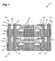
- FIG. 1 presents a cross-sectional view of one example of a semiconductor package fabricated using known techniques.
- semiconductor package 100 includes top active die 110 and bottom active die 130.
- Top active die 110 includes dielectric layer 116 situated on substrate 118.
- Top active die 110 includes transistors 112, which are examples of numerous transistors that are interconnected through interconnects 114.
- interconnects 114 may be partially disposed within dielectric layer 116.
- Interconnects 114 may further couple transistors 112 to through-silicon vias (TSV) 120.
- TSVs 120 may extend completely through dielectric layer 116 and substrate 118, as shown in Figure 1 .
- top active die 110 may include a different number of TSVs 120.
- top active die 110 may also include microbumps 122, which are connected to TSVs 120 in this implementation.
- Bottom active die 130 includes dielectric layer 136 situated on substrate 138.
- Bottom active die 130 includes transistors 132, which are interconnected through interconnects 134. As seen in Figure 1 , interconnects 134 may be partially disposed within dielectric layer 136. Interconnects 134 may further couple transistors 132 to TSVs 140. TSVs 140 may extend completely through dielectric layer 136 and substrate 138, as shown in Figure 1 . Although Figure 1 depicts bottom active die 130 having four TSVs 140, in other implementations, bottom active die 130 may include a different number of TSVs 140.
- bottom active die 130 also includes microbumps 142, which may be connected to TSVs 140. Further, microbumps 142 attach top active die 110 to bottom active die 130. Microbumps 142 may electrically and mechanically connect TSVs 120 to TSVs 140.
- top active die 110 and bottom active die 130 are similar in size and complexity. However, in other implementations, top active die 110 and bottom active die 130 may not be similar. Furthermore, in other implementations, semiconductor package 100 may include other features not shown in Figure 1 for the purpose of brevity of discussion.
- interconnects 114 and 134 are examples of signal paths for top active die 110 and bottom active die 130, respectively.
- transient currents running through interconnects 134 generate electromagnetic field 102.
- an electric field portion of electromagnetic field 102 is depicted as dashed arrows, and a magnetic field portion of electromagnetic field 102 is depicted as dotted ellipses.
- electromagnetic field 102 causes electromagnetic coupling between interconnects 114 and 134, thus creating electromagnetic noise.
- Electromagnetic noise due to electromagnetic field 102 undesirably generates crosstalk noise in signals transmitted by interconnects 114 and 134.
- electromagnetic field 102 induces a current in interconnects 114 due to a magnetic field generated by a current in interconnects 134. Electromagnetic field 102 may also cause capacitive coupling between interconnects 114 and 134 due to an electric field generated by interconnects 134.
- the crosstalk noise may not be limited to top active die 110 and bottom active die 130, as electromagnetic coupling may occur between additional or non-adjacent dies in the stack (not shown in Figure 1 ). Even if the crosstalk noise is of little amplitude, crosstalk noise on the signal could impair functionality of the active dies.
- Figure 2 presents a cross-sectional view of a semiconductor package including one implementation of a shield interposer.
- semiconductor package 200 includes bottom active die 230, shield interposer 250, and top active die 210.
- Top active die 210 may correspond to top active die 110 in Figure 1 .
- Bottom active die 230 may correspond to bottom active die 130 in Figure 1 .
- Top active die 210 includes dielectric layer 216 situated on substrate 218. Top active die 210 also includes transistors 212, which are interconnected through interconnects 214. As seen in Figure 2 , interconnects 214 may be partially disposed within dielectric layer 216. Interconnects 214 may further couple transistors 212 to TSVs 220. TSVs 220 may extend completely through dielectric layer 216 and substrate 218, as shown in Figure 2 . Although Figure 2 depicts top active die 210 having four TSVs 220, in other implementations, top active die 210 may include a different number of TSVs 220. In addition, top active die 210 also includes microbumps 222, which may be connected to TSVs 220.
- transistors 212, interconnects 214, dielectric layer 216, substrate 218, TSVs 220, and microbumps 222 may correspond, respectively, to transistors 112, interconnects 114, dielectric layer 116, substrate 118, TSVs 120, and microbumps 122 in Figure 1 .
- Bottom active die 230 includes dielectric layer 236 situated on substrate 238. Bottom active die 230 also includes transistors 232, which are interconnected through interconnects 234. As seen in Figure 2 , interconnects 234 may be partially disposed within dielectric layer 236. Interconnects 234 may further couple transistors 232 to TSVs 240. TSVs 240 may extend completely through dielectric layer 236 and substrate 238, as shown in Figure 2 . Although Figure 2 depicts bottom active die 230 having four TSVs 240, in other implementations, bottom active die 230 may include a different number of TSVs 240. In addition, bottom active die 230 also includes microbumps 242, which may be connected to TSVs 240. Further, microbumps 242 attach shield interposer 250 to bottom active die 230. Microbumps 242 electrically and mechanically connect TSVs 240 to TSVs 260, 270, and 272.
- top active die 210 and bottom active die 230 are similar in size and complexity, in other implementations, top active die 210 and bottom active die 230 may not be similar.
- transistors 232, interconnects 234, dielectric layer 236, substrate 238, TSVs 240, and microbumps 242 may correspond, respectively, to transistors 132, interconnects 134, dielectric layer 136, substrate 138, TSVs 140, and microbumps 142 in Figure 1 .
- Shield interposer 250 includes dielectric layer 256 situated on substrate 258. Shield interposer 250 further includes electromagnetic shield 252 and electromagnetic shield 254. In the implementation shown in Figure 2 , electromagnetic shield 252 is coupled to an outermost TSV near electromagnetic shield 252, i.e. TSV 270. Similarly, electromagnetic shield 254 is coupled to an outermost TSV near electromagnetic shield 254, i.e. TSV 272 in Figure 2 . Electromagnetic shields 252 and 254 may be disposed entirely within dielectric layer 256. As depicted in Figure 2 , electromagnetic shield 254 overlaps electromagnetic shield 252 within dielectric layer 256. In the present example, electromagnetic shields 252 and 254 overlap without contacting each other.
- electromagnetic shields 252 and 254 may be coupled to respective fixed potentials. Electromagnetic shield 252 may be coupled to a Vdd (or a ground) potential whereas electromagnetic shield 254 may be coupled to a ground (or Vdd) potential.
- electromagnetic shields 252 and 254 may not, for example, overlap.
- electromagnetic shields 252 and 253 may have smaller dimensions than depicted in Figure 2 so that they do not overlap within dielectric layer 256.
- electromagnetic shields 252 and 254 may be coupled to each other, or otherwise coupled to the same fixed potential.
- electromagnetic shields 252 and 254 may be coupled to any other fixed potentials.
- electromagnetic shields 252 and 254 may be coupled to other TSVs 260, 270, and 272.
- electromagnetic shields 252 and 254 may be directly connected to respective fixed potentials, or may be connected through any other means, such as through interconnects 264 and 266 and microbumps 262.
- TSVs 260, 270, and 272 may extend completely through dielectric layer 256 and substrate 258, as shown in Figure 2 .
- Figure 2 depicts shield interposer 250 including four TSVs, in other implementations, shield interposer 250 may include a different number of TSVs.
- Shield interposer 250 also includes microbumps 262, which may connect TSVs 260, 270, and 272 respectively to TSVs 220, as seen in Figure 2 .
- Microbumps 262 further attaches top active die 210 to shield interposer 250. Also shown in Figure 2 , top active die 210, shield interposer 250, and bottom active die 230 may be electrically connected through at least TSVs 220, 260, 270, 272, and 240, and microbumps 262 and 242.
- electromagnetic field 202 During normal operation, transient currents running through interconnects 234 of bottom active die 230 generate electromagnetic field 202.
- an electric field portion of electromagnetic field 202 is depicted as dashed arrows, and a magnetic field portion of electromagnetic field 202 is depicted as dotted ellipses.
- shield interposer 250 shields interconnects 214 of top active die 210 from being electromagnetically coupled to interconnects 234 of bottom active die 230.
- electromagnetic field 202 causes interconnects 234 to be electromagnetically coupled to electromagnetic shields 252 and 254 rather than interconnects 214. In effect, shield interposer 250 substantially terminates electromagnetic field 202.
- electromagnetic field 202 induces a current in electromagnetic shields 252 and 254 rather than interconnects 214. Electromagnetic field 202 may also cause capacitive coupling between interconnects 234 and electromagnetic shields 252 and 254 rather than interconnects 214.
- residual electromagnetic field 204 may still electromagnetically couple interconnect 214 of top active die 210 with interconnect 234 of bottom active die 230, as seen in Figure 2 .
- electromagnetic noise due to electromagnetic field 202 is significantly reduced.
- semiconductor package 200, having shield interposer 250 may advantageously have reduced electromagnetic noise relative to semiconductor package 100, having no shield interposer.
- electromagnetic shields 252 and 254 are connected to fixed potentials. By connecting electromagnetic shields 252 and 254 to potentials, shield interposer 250 provides an additional advantage of decoupling capacitance, which may provide further benefits to power integrity.
- electromagnetic shield 252 is connected to Vdd
- electromagnetic shield 254 is connected to ground. As such, electromagnetic shields 252 and 254 can provide decoupling capacitance between Vdd and ground.
- Figures 3A and 3B present one implementation of a shield interposer.
- Figure 3A presents a cross-sectional view of shield interposer 350
- Figure 3B presents a top-down view of shield interposer 350.
- Shield interposer 350 may correspond to shield interposer 250 in Figure 2 .
- dielectric layer 356, substrate 358, TSVs 360, microbumps 362, interconnects 364, interconnects 366, TSV 370, TSV 372, electromagnetic shield 352, and electromagnetic shield 354 may correspond, respectively, to dielectric layer 256, substrate 258, TSVs 260, microbumps 262, interconnects 264, interconnects 266, TSV 270, TSV 272, electromagnetic shield 252, and electromagnetic shield 254 in Figure 2 .
- dielectric layer 356, substrate 358, TSVs 360, microbumps 362, interconnects 364, interconnects 366, TSV 370, TSV 372, electromagnetic shield 352, and electromagnetic shield 354 may correspond, respectively, to dielectric layer 256, substrate 258, TSVs 260, microbumps 262, interconnects 264, interconnects 266, TSV 270, TSV 272, electromagnetic shield 252, and electromagnetic shield 254 in Figure 2 .
- shield interposer 350 and shield interposer 250 will not be discussed.
- substrate 358 is obscured by dielectric layer 356, and microbumps 362 are not shown.
- parts of dielectric layer 356 are not shown in order to depict interconnects 364 and 366, which are disposed on a top surface of dielectric layer 356, as well as electromagnetic shields 252 and 254, which are disposed within dielectric layer 356.
- Electromagnetic shields 352 and 354 are made of a conductive material, such as metal, arranged in grids. For instance, as seen in Figure 3B , electromagnetic shield 352 includes a grid of conductive layers. Electromagnetic shield 354 similarly includes a grid of conductive layers. As further seen in Figure 3A , electromagnetic shield 354 is disposed within dielectric layer 356, although above electromagnetic shield 352, which is also disposed within dielectric layer 356. This arrangement results in electromagnetic shield 354 at least partially overlapping electromagnetic shield 352, as depicted in Figures 3A and 3B . However, in other implementations, electromagnetic shields 352 and 354 may take on other shapes, such as a plate, and may also be configured to not overlap.
- FIG. 3B further shows one implementation of TSVs 360, 370, and 372.
- shield interposer 350 includes TSVs arranged in rows along outer edges of shield interposer 350, such as TSVs 370, and TSVs 372.
- Shield interposer 350 further includes inner rows of TSVs away from the outer edges, such as TSVs 360.
- This TSV arrangement may mirror TSV arrangements of active dies, such as top active die 210 and bottom active die 230 in Figure 2 .
- interconnects 364 connects electromagnetic shield 352 only to the TSVs along the outer edge, i.e. TSVs 370.
- interconnects 366 connects electromagnetic shield 354 only to the TSVs along the outer edge, i.e. TSVs 372.
- electromagnetic shields 352 and 354 may be connected to other TSVs 360.
- electromagnetic shields 352 and 354 are directly connected to the first and second fixed potentials, respectively.
- Figures 4 and 5 present alternative implementations for electrically connecting the electromagnetic shields.
- Figure 4 presents a cross-sectional view of a semiconductor package according to one implementation of a shield interposer.
- Figure 4 depicts semiconductor package 400, which includes bottom active die 430, shield interposer 450 situated on bottom active die 430, and top active die 410 situated on shield interposer 450.
- Bottom active die 430 which includes transistors 432, interconnects 434, dielectric layer 436, substrate 438, TSVs 440, and microbumps 442, may correspond, respectively, to bottom active die 230, transistors 232, interconnects 234, dielectric layer 236, substrate 238, TSVs 240, and microbumps 242 in Figure 2 .
- top active die 410 which includes transistors 412, interconnects 414, dielectric layer 416, substrate 418, TSVs 420, and microbumps 422, may correspond, respectively, to top active die 210, transistors 212, interconnects 214, dielectric layer 216, substrate 218, TSVs 220, and microbumps 222 in Figure 2 .
- top active die 410 and bottom active die 430 will not be discussed.
- Shield interposer 450 may correspond to shield interposer 250 in Figure 2 .
- electromagnetic shields 452 and 454, dielectric layer 456, substrate 458, TSVs 460, microbumps 462, interconnects 464 and 466, and TSV 470 and TSV 472 may correspond, respectively, to electromagnetic shields 252 and 254, dielectric layer 256, substrate 258, TSVs 260, microbumps 262, interconnects 264 and 266, and TSV 270 and TSV 272 in Figure 2 .
- dielectric layer 256, substrate 258, TSVs 260, microbumps 262, interconnects 264 and 266, and TSV 270 and TSV 272 in Figure 2 .
- similarities between shield interposer 450 and shield interposers 250 and 350 will not be discussed.
- shield interposer 450 differs from shield interposers 350 and 250 in its dimensions with respect to top active die 410 and bottom active die 430. As shown in Figure 4 , shield interposer 450 laterally extends beyond top active die 410 and bottom active die 430. Specifically in Figure 4 , shield interposer 450 laterally extends beyond top active die 410 and bottom active die 430 on two sides, which is not a limiting feature.
- TSVs 470 and 472 are disposed within portions of shield interposer 450 that laterally extend beyond top active die 410 and bottom active die 430.
- TSVs 470 and 472 are connected to electromagnetic shields 452 and 454 through interconnects 464 and 466, respectively.
- TSVs 470 and 472 are not connected to TSVs 440 of bottom active die 430 or TSVs 420 of top active die 410. Rather, TSVs 470 and 472 are connected to solder bumps 474.
- solder bumps 474 are disposed on a bottom surface of the portions of shield interposer 450 that laterally extend beyond top active die 410 and bottom active die 430.
- Solder bumps 474 may be connected to first and second fixed potentials, such as Vdd or ground.
- solder bumps 474 are conventional solder bumps, such as C4 bumps, which allows for easier connections external to semiconductor package 400.
- Solder bumps 474 are advantageously disposed outside the active die boundary. Solder bumps 474 may provide connection to the packaging substrate (not shown in Figure 4 ) on which semiconductor package 400 may be attached. Solder bumps 474 further allows for electromagnetic shields 452 and 454 to be electrically connected to potentials not available through TSVs of the active dies. For instance, in Figure 4 , TSVs 420, 460, and 440 along one side of semiconductor package 400 may be connected to a first potential, and TSVs 420, 460, and 440 along the other side may be connected to a second potential. However, TSVs 470 and 472 are electrically isolated from TSVs 420, 460, and 440. Therefore, TSVs 470 and 472 may connect electromagnetic shields 452 and 454 to third and fourth potentials, respectively, through solder bumps 474.
- FIG. 5 presents a cross-sectional view of another implementation of a shield interposer.
- Semiconductor package 500 includes bottom active die 530, shield interposer 550 situated on bottom active die 530, and top active die 510 situated on shield interposer 550.
- Bottom active die 530 which includes transistors 532, interconnects 534, dielectric layer 536, substrate 538, TSVs 540, and microbumps 542, may correspond, respectively, to bottom active die 230, transistors 232, interconnects 234, dielectric layer 236, substrate 238, TSVs 240, and microbumps 242 in Figure 2 .
- top active die 510 which includes transistors 512, interconnects 514, dielectric layer 516, substrate 518, TSVs 520, and microbumps 522, may correspond, respectively, to top active die 210, transistors 212, interconnects 214, dielectric layer 216, substrate 218, TSVs 220, and microbumps 222 in Figure 2 .
- top active die 510 and bottom active die 530 will not be discussed.
- Shield interposer 550 may correspond to shield interposer 250 in Figure 2 .
- electromagnetic shields 552 and 554, dielectric layer 556, substrate 558, TSVs 560, microbumps 562, and interconnects 564 and 566 may correspond, respectively, to electromagnetic shields 252 and 254, dielectric layer 256, substrate 258, TSVs 260, microbumps 262, and interconnects 264 and 266 in Figure 2 .
- dielectric layer 256, substrate 258, TSVs 260, microbumps 262, and interconnects 264 and 266 in Figure 2 .
- shield interposer 550 laterally extends beyond top active die 510 and bottom active die 530 on two sides, although the number of sides is not limiting.
- electromagnetic shield 552 and 554 may be electrically connected to potentials not available through any TSVs of the active dies.
- electromagnetic shields 552 and 554 are connected to the first and second fixed potentials through wirebonds 570 and 572.
- wirebonds 570 and 572 may be connected externally to semiconductor package 500.
- wirebonds 570 and 572 may be connected to potentials on the packaging substrate (not shown in Figure 5 ), which semiconductor package 500 is attached to.
- wirebonds 570 and 572 are connected to electromagnetic shields 552 and 554, respectively, through peripheral pads 576. Wirebonds 570 and 572 and peripheral pads 576 are disposed outside the active die boundary, as depicted in Figure 5 .
- Peripheral pads 576 are situated on a top surface of dielectric layer 556 of shield interposer 550. Specifically, peripheral pads 576 are disposed over portions of shield interposer 550 that laterally extend beyond top active die 510 and bottom active die 530, as shown in Figure 5 .
- Wirebonds 570 and 572 may be connected to Vdd and/or ground, or other fixed potentials. Wirebonds 570 and 572 allow for simpler external connections, and for further design flexibility.
- Wirebonds 570 and 572 provide the added benefit of additional electromagnetic shielding beyond the shielding provided by electromagnetic shields 552 and 554. As seen in Figure 5 , electromagnetic shields 552 and 554 are generally restricted to the size of top active die 510 and bottom active die 530. Because wirebonds 570 and 572 are connected to the same fixed potentials as electromagnetic shields 552 and 554, respectively, wirebonds 570 and 572 provide similar electromagnetic shielding. Wirebonds 570 and 572 extend beyond electromagnetic shields 552 and 554, and therefore may provide electromagnetic shielding along their respective sides of semiconductor package 500.
- various implementations of the concepts disclosed herein advantageously shield the active dies from electromagnetic noise.
- the disclosed implementations advantageously enable production of interposers having electromagnetic shields.
- the described implementations disclose a shield interposer situated between a top active die and a bottom active die, and has an interposer dielectric layer, TSVs passing through the interposer dielectric layer, and an electromagnetic shield connected to a fixed potential through the TSVs.
- the present concepts advantageously enable electromagnetic shielding between active dies stacked on each other.
Landscapes
- Engineering & Computer Science (AREA)
- Microelectronics & Electronic Packaging (AREA)
- Shielding Devices Or Components To Electric Or Magnetic Fields (AREA)
- Internal Circuitry In Semiconductor Integrated Circuit Devices (AREA)
- Semiconductor Integrated Circuits (AREA)
Abstract
Description
- There is an ever increasing need for reducing the size of semiconductor packages while increasing functionality. This need typically results in semiconductor package designs to accommodate more than one semiconductor die, where each die can be a complex die containing numerous transistors and multi-level interconnects. During operation, the complex dies generate large amounts of transient currents running through various interconnects on the dies. The large transient currents and the accompanying transient voltages in turn result in a great amount of electromagnetic noise generated by each die. Since advanced packages include multiple dies in close proximity, electromagnetic noise from one die has a great undesired impact in other dies in the package. More specifically, electromagnetic noise generated by one die typically induces undesired noise currents and noise voltages in the other dies in the package. The problem of inducing undesired noise is aggravated due to the reduction in size of semiconductor packages, and the reduction of separation between adjacent dies, and when more than two dies are housed in the same package.
- Further, each semiconductor package may be exposed to external electromagnetic noise from other components in a system, such as other noisy semiconductor packages. Reduction of impact of electromagnetic noise is an important goal of advanced packaging design.
- The present disclosure is directed to a semiconductor package with integrated electromagnetic shielding, substantially as shown in and/or described in connection with at least one of the figures, as set forth more completely in the claims.
- According to an aspect, a shield interposer is provided situated between a top active die and a bottom active die for shielding said top active die and said bottom active die from electromagnetic noise, said shield interposer comprising:
- an interposer dielectric layer;
- a through-silicon via (TSV) within said interposer dielectric layer;
- an electromagnetic shield connected to a fixed potential through said TSV.
- Advantageously, said electromagnetic shield comprises a grid of conductive layers.
- Advantageously, said electromagnetic shield is disposed entirely within said interposer dielectric layer.
- Advantageously, said electromagnetic shield is partially disposed within said interposer dielectric layer.
- Advantageously, said fixed potential is a ground potential.
- Advantageously, said fixed potential is a Vdd potential.
- Advantageously, the shield interposer further comprises another electromagnetic shield connected to another fixed potential.
- Advantageously, said another electromagnetic shield at least partially overlaps said electromagnetic shield.
- Advantageously, said fixed potential is a Vdd potential, and said another fixed potential is a ground potential.
- According to an aspect, a semiconductor package comprises:
- a bottom active die;
- a shield interposer situated over said bottom active die;
- a top active die situated over said shield interposer for shielding said top active die and said bottom active die from electromagnetic noise;
- said shield interposer having an interposer dielectric layer, a through-silicon via (TSV) within said interposer dielectric layer, and an electromagnetic shield connected to a fixed potential through said TSV.
- Advantageously, said shield interposer laterally extends beyond said bottom active die and said top active die.
- Advantageously, a portion of said shield interposer laterally extends beyond said bottom active die and said top active die, said TSV situated within said portion of said shield interposer;
said shield interposer further comprising a solder bump situated on a bottom surface of said portion of said shield interposer, said solder bump connected to said TSV. - Advantageously, said electromagnetic shield comprises a grid of conductive layers.
- Advantageously, said electromagnetic shield is disposed entirely within said interposer dielectric layer.
- Advantageously, said fixed potential is a ground potential or a Vdd potential.
- According to an aspect, a semiconductor package comprises:
- a bottom active die;
- a shield interposer situated over said bottom active die;
- a top active die situated over said shield interposer for shielding said top active die and said bottom active die from electromagnetic noise;
- said shield interposer having an electromagnetic shield connected to a fixed potential through a wirebond.
- Advantageously, a portion of said shield interposer laterally extends beyond said bottom active die and said top active die;
said shield interposer further comprising a peripheral pad situated on a top surface of said portion of said shield interposer, said peripheral pad connected to said electromagnetic shield, and said wirebond connected to said peripheral pad. - Advantageously, said electromagnetic shield comprises a grid of conductive layers.
- Advantageously, said shield interposer further comprises an interposer dielectric layer, said electromagnetic shield disposed entirely within said interposer dielectric layer.
- Advantageously, said fixed potential is a ground potential or a Vdd potential.
-
-
Figure 1 shows a cross-sectional view of one implementation of a semiconductor package having a top active die stacked on a bottom active die. -
Figure 2 shows a cross-sectional view of one implementation of a semiconductor package having a top active die stacked on a shield interposer, further stacked on a bottom active die. -
Figure 3A shows a cross-sectional view of one implementation of a shield interposer. -
Figure 3B shows a top-down view of the shield interposer shown inFigure 3A . -
Figure 4 shows a cross-sectional view of one implementation of a semiconductor package including a shield interposer having solder bumps. -
Figure 5 shows a cross-sectional view of one implementation of a semiconductor package including a shield interposer having wirebonds. - The following description contains specific information pertaining to implementations in the present disclosure. One skilled in the art will recognize that the present disclosure may be implemented in a manner different from that specifically discussed herein. The drawings in the present application and their accompanying detailed description are directed to merely exemplary implementations. Unless noted otherwise, like or corresponding elements among the figures may be indicated by like or corresponding reference numerals. Moreover, the drawings and illustrations in the present application are generally not to scale, and are not intended to correspond to actual relative dimensions.
-
Figure 1 presents a cross-sectional view of one example of a semiconductor package fabricated using known techniques. As depicted inFigure 1 ,semiconductor package 100 includes topactive die 110 and bottomactive die 130. Top active die 110 includesdielectric layer 116 situated onsubstrate 118. Topactive die 110 includestransistors 112, which are examples of numerous transistors that are interconnected throughinterconnects 114. As seen inFigure 1 ,interconnects 114 may be partially disposed withindielectric layer 116.Interconnects 114 mayfurther couple transistors 112 to through-silicon vias (TSV) 120.TSVs 120 may extend completely throughdielectric layer 116 andsubstrate 118, as shown inFigure 1 . AlthoughFigure 1 depicts topactive die 110 having fourTSVs 120, in other implementations, topactive die 110 may include a different number ofTSVs 120. In addition, topactive die 110 may also includemicrobumps 122, which are connected toTSVs 120 in this implementation. - Bottom
active die 130 includesdielectric layer 136 situated onsubstrate 138. Bottomactive die 130 includestransistors 132, which are interconnected throughinterconnects 134. As seen inFigure 1 , interconnects 134 may be partially disposed withindielectric layer 136.Interconnects 134 may further coupletransistors 132 toTSVs 140.TSVs 140 may extend completely throughdielectric layer 136 andsubstrate 138, as shown inFigure 1 . AlthoughFigure 1 depicts bottomactive die 130 having fourTSVs 140, in other implementations, bottomactive die 130 may include a different number ofTSVs 140. In addition, bottomactive die 130 also includesmicrobumps 142, which may be connected toTSVs 140. Further, microbumps 142 attach topactive die 110 to bottomactive die 130.Microbumps 142 may electrically and mechanically connectTSVs 120 toTSVs 140. - In
Figure 1 , topactive die 110 and bottomactive die 130 are similar in size and complexity. However, in other implementations, topactive die 110 and bottomactive die 130 may not be similar. Furthermore, in other implementations,semiconductor package 100 may include other features not shown inFigure 1 for the purpose of brevity of discussion. - When current flows through signal paths of a semiconductor die, typically interconnect metal in various metal layers, electromagnetic fields and noise are generated. In
semiconductor package 100,interconnects active die 110 and bottomactive die 130, respectively. During normal operation, transient currents running throughinterconnects 134 generateelectromagnetic field 102. InFigure 1 , an electric field portion ofelectromagnetic field 102 is depicted as dashed arrows, and a magnetic field portion ofelectromagnetic field 102 is depicted as dotted ellipses. As seen inFigure 1 ,electromagnetic field 102 causes electromagnetic coupling betweeninterconnects electromagnetic field 102 undesirably generates crosstalk noise in signals transmitted byinterconnects - More specifically,
electromagnetic field 102 induces a current ininterconnects 114 due to a magnetic field generated by a current ininterconnects 134.Electromagnetic field 102 may also cause capacitive coupling betweeninterconnects interconnects 134. In addition, the crosstalk noise may not be limited to topactive die 110 and bottomactive die 130, as electromagnetic coupling may occur between additional or non-adjacent dies in the stack (not shown inFigure 1 ). Even if the crosstalk noise is of little amplitude, crosstalk noise on the signal could impair functionality of the active dies. - Turning to
Figure 2, Figure 2 presents a cross-sectional view of a semiconductor package including one implementation of a shield interposer. As depicted inFigure 2 ,semiconductor package 200 includes bottomactive die 230,shield interposer 250, and topactive die 210. Topactive die 210 may correspond to topactive die 110 inFigure 1 . Bottomactive die 230 may correspond to bottomactive die 130 inFigure 1 . - Top
active die 210 includesdielectric layer 216 situated onsubstrate 218. Topactive die 210 also includestransistors 212, which are interconnected throughinterconnects 214. As seen inFigure 2 , interconnects 214 may be partially disposed withindielectric layer 216.Interconnects 214 may further coupletransistors 212 toTSVs 220.TSVs 220 may extend completely throughdielectric layer 216 andsubstrate 218, as shown inFigure 2 . AlthoughFigure 2 depicts topactive die 210 having fourTSVs 220, in other implementations, topactive die 210 may include a different number ofTSVs 220. In addition, topactive die 210 also includesmicrobumps 222, which may be connected toTSVs 220. - Further,
transistors 212, interconnects 214,dielectric layer 216,substrate 218,TSVs 220, andmicrobumps 222 may correspond, respectively, totransistors 112, interconnects 114,dielectric layer 116,substrate 118,TSVs 120, and microbumps 122 inFigure 1 . - Bottom
active die 230 includesdielectric layer 236 situated onsubstrate 238. Bottomactive die 230 also includestransistors 232, which are interconnected throughinterconnects 234. As seen inFigure 2 , interconnects 234 may be partially disposed withindielectric layer 236.Interconnects 234 may further coupletransistors 232 toTSVs 240.TSVs 240 may extend completely throughdielectric layer 236 andsubstrate 238, as shown inFigure 2 . AlthoughFigure 2 depicts bottomactive die 230 having fourTSVs 240, in other implementations, bottomactive die 230 may include a different number ofTSVs 240. In addition, bottomactive die 230 also includesmicrobumps 242, which may be connected toTSVs 240. Further, microbumps 242 attachshield interposer 250 to bottomactive die 230.Microbumps 242 electrically and mechanically connectTSVs 240 toTSVs - Although in
Figure 2 topactive die 210 and bottomactive die 230 are similar in size and complexity, in other implementations, topactive die 210 and bottomactive die 230 may not be similar. Further,transistors 232, interconnects 234,dielectric layer 236,substrate 238,TSVs 240, andmicrobumps 242 may correspond, respectively, totransistors 132, interconnects 134,dielectric layer 136,substrate 138,TSVs 140, and microbumps 142 inFigure 1 . -
Shield interposer 250 includesdielectric layer 256 situated onsubstrate 258.Shield interposer 250 further includeselectromagnetic shield 252 andelectromagnetic shield 254. In the implementation shown inFigure 2 ,electromagnetic shield 252 is coupled to an outermost TSV nearelectromagnetic shield 252, i.e.TSV 270. Similarly,electromagnetic shield 254 is coupled to an outermost TSV nearelectromagnetic shield 254, i.e.TSV 272 inFigure 2 .Electromagnetic shields dielectric layer 256. As depicted inFigure 2 ,electromagnetic shield 254 overlapselectromagnetic shield 252 withindielectric layer 256. In the present example,electromagnetic shields electromagnetic shields Electromagnetic shield 252 may be coupled to a Vdd (or a ground) potential whereaselectromagnetic shield 254 may be coupled to a ground (or Vdd) potential. -
Figure 2 presents an exemplary implementation ofelectromagnetic shields electromagnetic shields electromagnetic shields 252 and 253 may have smaller dimensions than depicted inFigure 2 so that they do not overlap withindielectric layer 256. In other implementations,electromagnetic shields electromagnetic shields electromagnetic shields other TSVs electromagnetic shields interconnects microbumps 262. -
TSVs dielectric layer 256 andsubstrate 258, as shown inFigure 2 . AlthoughFigure 2 depictsshield interposer 250 including four TSVs, in other implementations,shield interposer 250 may include a different number of TSVs.Shield interposer 250 also includesmicrobumps 262, which may connectTSVs TSVs 220, as seen inFigure 2 .Microbumps 262 further attaches topactive die 210 to shieldinterposer 250. Also shown inFigure 2 , topactive die 210,shield interposer 250, and bottomactive die 230 may be electrically connected through at least TSVs 220, 260, 270, 272, and 240, andmicrobumps - During normal operation, transient currents running through
interconnects 234 of bottomactive die 230 generateelectromagnetic field 202. InFigure 2 , an electric field portion ofelectromagnetic field 202 is depicted as dashed arrows, and a magnetic field portion ofelectromagnetic field 202 is depicted as dotted ellipses. In contrast toFigure 1 , however,shield interposer 250shields interconnects 214 of top active die 210 from being electromagnetically coupled tointerconnects 234 of bottomactive die 230. In particular,electromagnetic field 202 causesinterconnects 234 to be electromagnetically coupled toelectromagnetic shields shield interposer 250 substantially terminateselectromagnetic field 202. For example,electromagnetic field 202 induces a current inelectromagnetic shields Electromagnetic field 202 may also cause capacitive coupling betweeninterconnects 234 andelectromagnetic shields - However, residual
electromagnetic field 204 may still electromagneticallycouple interconnect 214 of topactive die 210 withinterconnect 234 of bottomactive die 230, as seen inFigure 2 . Compared toelectromagnetic field 102 inFigure 1 , electromagnetic noise due toelectromagnetic field 202 is significantly reduced. As such,semiconductor package 200, havingshield interposer 250, may advantageously have reduced electromagnetic noise relative tosemiconductor package 100, having no shield interposer. - As further seen in
Figure 2 ,electromagnetic shields electromagnetic shields shield interposer 250 provides an additional advantage of decoupling capacitance, which may provide further benefits to power integrity. For example, inFigure 2 ,electromagnetic shield 252 is connected to Vdd, andelectromagnetic shield 254 is connected to ground. As such,electromagnetic shields - Turning to
Figures 3A and 3B, Figures 3A and 3B present one implementation of a shield interposer.Figure 3A presents a cross-sectional view ofshield interposer 350, andFigure 3B presents a top-down view ofshield interposer 350.Shield interposer 350 may correspond to shield interposer 250 inFigure 2 . Specifically,dielectric layer 356,substrate 358,TSVs 360,microbumps 362, interconnects 364, interconnects 366,TSV 370,TSV 372,electromagnetic shield 352, andelectromagnetic shield 354 may correspond, respectively, todielectric layer 256,substrate 258,TSVs 260,microbumps 262, interconnects 264, interconnects 266,TSV 270,TSV 272,electromagnetic shield 252, andelectromagnetic shield 254 inFigure 2 . For the sake of brevity, similarities betweenshield interposer 350 andshield interposer 250 will not be discussed. - In
Figure 3B ,substrate 358 is obscured bydielectric layer 356, and microbumps 362 are not shown. In addition, parts ofdielectric layer 356 are not shown in order to depictinterconnects dielectric layer 356, as well aselectromagnetic shields dielectric layer 356. -
Electromagnetic shields Figure 3B ,electromagnetic shield 352 includes a grid of conductive layers.Electromagnetic shield 354 similarly includes a grid of conductive layers. As further seen inFigure 3A ,electromagnetic shield 354 is disposed withindielectric layer 356, although aboveelectromagnetic shield 352, which is also disposed withindielectric layer 356. This arrangement results inelectromagnetic shield 354 at least partially overlappingelectromagnetic shield 352, as depicted inFigures 3A and 3B . However, in other implementations,electromagnetic shields -
Figure 3B further shows one implementation ofTSVs Figure 3B ,shield interposer 350 includes TSVs arranged in rows along outer edges ofshield interposer 350, such asTSVs 370, andTSVs 372.Shield interposer 350 further includes inner rows of TSVs away from the outer edges, such asTSVs 360. This TSV arrangement may mirror TSV arrangements of active dies, such as topactive die 210 and bottomactive die 230 inFigure 2 . - In the implementation depicted in
Figure 3B , interconnects 364 connectselectromagnetic shield 352 only to the TSVs along the outer edge, i.e.TSVs 370. Similarly, interconnects 366 connectselectromagnetic shield 354 only to the TSVs along the outer edge, i.e.TSVs 372. In other implementations,electromagnetic shields other TSVs 360. - In
Figures 3A and 3B ,electromagnetic shields Figures 4 and5 present alternative implementations for electrically connecting the electromagnetic shields. - Turning now to
Figure 4, Figure 4 presents a cross-sectional view of a semiconductor package according to one implementation of a shield interposer.Figure 4 depictssemiconductor package 400, which includes bottomactive die 430,shield interposer 450 situated on bottomactive die 430, and topactive die 410 situated onshield interposer 450. Bottomactive die 430, which includestransistors 432, interconnects 434,dielectric layer 436,substrate 438,TSVs 440, andmicrobumps 442, may correspond, respectively, to bottomactive die 230,transistors 232, interconnects 234,dielectric layer 236,substrate 238,TSVs 240, and microbumps 242 inFigure 2 . Likewise, topactive die 410, which includestransistors 412, interconnects 414,dielectric layer 416,substrate 418,TSVs 420, andmicrobumps 422, may correspond, respectively, to topactive die 210,transistors 212, interconnects 214,dielectric layer 216,substrate 218,TSVs 220, and microbumps 222 inFigure 2 . For the sake of brevity, topactive die 410 and bottomactive die 430 will not be discussed. -
Shield interposer 450 may correspond to shield interposer 250 inFigure 2 . In addition,electromagnetic shields dielectric layer 456,substrate 458,TSVs 460,microbumps 462,interconnects TSV 470 andTSV 472 may correspond, respectively, toelectromagnetic shields dielectric layer 256,substrate 258,TSVs 260,microbumps 262,interconnects TSV 270 andTSV 272 inFigure 2 . For the sake of brevity, similarities betweenshield interposer 450 and shieldinterposers - In the implementation depicted in
Figure 4 ,shield interposer 450 differs fromshield interposers active die 410 and bottomactive die 430. As shown inFigure 4 ,shield interposer 450 laterally extends beyond topactive die 410 and bottomactive die 430. Specifically inFigure 4 ,shield interposer 450 laterally extends beyond topactive die 410 and bottomactive die 430 on two sides, which is not a limiting feature. -
TSVs shield interposer 450 that laterally extend beyond topactive die 410 and bottomactive die 430.TSVs electromagnetic shields interconnects TSVs active die 430 orTSVs 420 of topactive die 410. Rather,TSVs Figure 4 , solder bumps 474 are disposed on a bottom surface of the portions ofshield interposer 450 that laterally extend beyond topactive die 410 and bottomactive die 430. Solder bumps 474 may be connected to first and second fixed potentials, such as Vdd or ground. InFigure 4 , solder bumps 474 are conventional solder bumps, such as C4 bumps, which allows for easier connections external tosemiconductor package 400. - Solder bumps 474 are advantageously disposed outside the active die boundary. Solder bumps 474 may provide connection to the packaging substrate (not shown in
Figure 4 ) on whichsemiconductor package 400 may be attached. Solder bumps 474 further allows forelectromagnetic shields Figure 4 ,TSVs semiconductor package 400 may be connected to a first potential, andTSVs TSVs TSVs TSVs electromagnetic shields - Referring to
Figure 5, Figure 5 presents a cross-sectional view of another implementation of a shield interposer.Semiconductor package 500 includes bottomactive die 530,shield interposer 550 situated on bottomactive die 530, and topactive die 510 situated onshield interposer 550. Bottomactive die 530, which includestransistors 532, interconnects 534,dielectric layer 536,substrate 538,TSVs 540, andmicrobumps 542, may correspond, respectively, to bottomactive die 230,transistors 232, interconnects 234,dielectric layer 236,substrate 238,TSVs 240, and microbumps 242 inFigure 2 . Likewise, topactive die 510, which includestransistors 512, interconnects 514,dielectric layer 516,substrate 518,TSVs 520, andmicrobumps 522, may correspond, respectively, to topactive die 210,transistors 212, interconnects 214,dielectric layer 216,substrate 218,TSVs 220, and microbumps 222 inFigure 2 . For the sake of brevity, topactive die 510 and bottomactive die 530 will not be discussed. -
Shield interposer 550 may correspond to shield interposer 250 inFigure 2 . In addition,electromagnetic shields dielectric layer 556,substrate 558,TSVs 560,microbumps 562, and interconnects 564 and 566 may correspond, respectively, toelectromagnetic shields dielectric layer 256,substrate 258,TSVs 260,microbumps 262, and interconnects 264 and 266 inFigure 2 . For the sake of brevity, similarities betweenshield interposer 450 and shieldinterposers - Similar to shield interposer 450 in
Figure 4 ,shield interposer 550 laterally extends beyond topactive die 510 and bottomactive die 530 on two sides, although the number of sides is not limiting. In addition, similar toelectromagnetic shields electromagnetic shield shield interposer 450,electromagnetic shields wirebonds Figure 5 , wirebonds 570 and 572 may be connected externally tosemiconductor package 500. For example, wirebonds 570 and 572 may be connected to potentials on the packaging substrate (not shown inFigure 5 ), whichsemiconductor package 500 is attached to. Further, wirebonds 570 and 572 are connected toelectromagnetic shields peripheral pads 576.Wirebonds peripheral pads 576 are disposed outside the active die boundary, as depicted inFigure 5 . -
Peripheral pads 576 are situated on a top surface ofdielectric layer 556 ofshield interposer 550. Specifically,peripheral pads 576 are disposed over portions ofshield interposer 550 that laterally extend beyond topactive die 510 and bottomactive die 530, as shown inFigure 5 .Wirebonds Wirebonds -
Wirebonds electromagnetic shields Figure 5 ,electromagnetic shields active die 510 and bottomactive die 530. Becausewirebonds electromagnetic shields Wirebonds electromagnetic shields semiconductor package 500. - Thus, by situating electromagnetic shields between active regions of stacked active dies, various implementations of the concepts disclosed herein advantageously shield the active dies from electromagnetic noise. In addition, the disclosed implementations advantageously enable production of interposers having electromagnetic shields. The described implementations disclose a shield interposer situated between a top active die and a bottom active die, and has an interposer dielectric layer, TSVs passing through the interposer dielectric layer, and an electromagnetic shield connected to a fixed potential through the TSVs. As a result, the present concepts advantageously enable electromagnetic shielding between active dies stacked on each other.
- From the above description it is manifest that various techniques can be used for implementing the concepts described in the present application without departing from the scope of those concepts. Moreover, while the concepts have been described with specific reference to certain implementations, a person of ordinary skill in the art would recognize that changes can be made in form and detail without departing from the spirit and the scope of those concepts. As such, the described implementations are to be considered in all respects as illustrative and not restrictive. It should also be understood that the present application is not limited to the particular implementations described herein, but many rearrangements, modifications, and substitutions are possible without departing from the scope of the present disclosure.
Claims (15)
- A shield interposer situated between a top active die and a bottom active die for shielding said top active die and said bottom active die from electromagnetic noise, said shield interposer comprising:an interposer dielectric layer;a through-silicon via (TSV) within said interposer dielectric layer;an electromagnetic shield connected to a fixed potential through said TSV.
- The shield interposer of claim 1, wherein said electromagnetic shield comprises a grid of conductive layers.
- The shield interposer of claim 1, wherein said electromagnetic shield is disposed entirely within said interposer dielectric layer.
- The shield interposer of claim 1, wherein said electromagnetic shield is partially disposed within said interposer dielectric layer.
- The shield interposer of claim 1, wherein said fixed potential is a ground potential.
- The shield interposer of claim 1, wherein said fixed potential is a Vdd potential.
- The shield interposer of claim 1, further comprising another electromagnetic shield connected to another fixed potential.
- The shield interposer of claim 7, wherein said another electromagnetic shield at least partially overlaps said electromagnetic shield.
- The shield interposer of claim 7, wherein said fixed potential is a Vdd potential, and said another fixed potential is a ground potential.
- A semiconductor package comprising:a bottom active die;a shield interposer situated over said bottom active die;a top active die situated over said shield interposer for shielding said top active die and said bottom active die from electromagnetic noise;said shield interposer having an interposer dielectric layer, a through-silicon via (TSV) within said interposer dielectric layer, and an electromagnetic shield connected to a fixed potential through said TSV.
- The semiconductor package of claim 10, wherein said shield interposer laterally extends beyond said bottom active die and said top active die.
- The semiconductor package of claim 10, wherein a portion of said shield interposer laterally extends beyond said bottom active die and said top active die, said TSV situated within said portion of said shield interposer;
said shield interposer further comprising a solder bump situated on a bottom surface of said portion of said shield interposer, said solder bump connected to said TSV. - The semiconductor package of claim 10, wherein said electromagnetic shield comprises a grid of conductive layers.
- The semiconductor package of claim 10, wherein said electromagnetic shield is disposed entirely within said interposer dielectric layer.
- A semiconductor package comprising:a bottom active die;a shield interposer situated over said bottom active die;a top active die situated over said shield interposer for shielding said top active die and said bottom active die from electromagnetic noise;said shield interposer having an electromagnetic shield connected to a fixed potential through a wirebond.
Applications Claiming Priority (1)
| Application Number | Priority Date | Filing Date | Title |
|---|---|---|---|
| US13/405,721 US8928128B2 (en) | 2012-02-27 | 2012-02-27 | Semiconductor package with integrated electromagnetic shielding |
Publications (3)
| Publication Number | Publication Date |
|---|---|
| EP2631944A2 true EP2631944A2 (en) | 2013-08-28 |
| EP2631944A3 EP2631944A3 (en) | 2014-07-02 |
| EP2631944B1 EP2631944B1 (en) | 2019-01-02 |
Family
ID=46940192
Family Applications (1)
| Application Number | Title | Priority Date | Filing Date |
|---|---|---|---|
| EP12006332.6A Active EP2631944B1 (en) | 2012-02-27 | 2012-09-07 | Semiconductor package with integrated electromagnetic shielding |
Country Status (5)
| Country | Link |
|---|---|
| US (1) | US8928128B2 (en) |
| EP (1) | EP2631944B1 (en) |
| KR (1) | KR101355054B1 (en) |
| CN (2) | CN202871784U (en) |
| TW (1) | TWI543329B (en) |
Cited By (1)
| Publication number | Priority date | Publication date | Assignee | Title |
|---|---|---|---|---|
| TWI756339B (en) * | 2017-01-13 | 2022-03-01 | 台灣積體電路製造股份有限公司 | Semiconductor structure and manufacturing method thereof |
Families Citing this family (30)
| Publication number | Priority date | Publication date | Assignee | Title |
|---|---|---|---|---|
| US9048222B2 (en) | 2013-03-06 | 2015-06-02 | Taiwan Semiconductor Manufacturing Company, Ltd. | Method of fabricating interconnect structure for package-on-package devices |
| US20140339688A1 (en) * | 2013-05-15 | 2014-11-20 | Cavendish Kinetics, Inc. | Techniques for the cancellation of chip scale packaging parasitic losses |
| US9214433B2 (en) * | 2013-05-21 | 2015-12-15 | Xilinx, Inc. | Charge damage protection on an interposer for a stacked die assembly |
| US9530730B2 (en) | 2013-11-08 | 2016-12-27 | Taiwan Semiconductor Manufacturing Company, Ltd. | Configurable routing for packaging applications |
| US9583420B2 (en) | 2015-01-23 | 2017-02-28 | Taiwan Semiconductor Manufacturing Company, Ltd. | Semiconductor device and method of manufactures |
| US9281297B2 (en) | 2014-03-07 | 2016-03-08 | Taiwan Semiconductor Manufacturing Company, Ltd. | Solution for reducing poor contact in info packages |
| US9786633B2 (en) | 2014-04-23 | 2017-10-10 | Massachusetts Institute Of Technology | Interconnect structures for fine pitch assembly of semiconductor structures and related techniques |
| US9449947B2 (en) * | 2014-07-01 | 2016-09-20 | Taiwan Semiconductor Manufacturing Company, Ltd. | Semiconductor package for thermal dissipation |
| US10079224B2 (en) | 2014-08-11 | 2018-09-18 | Massachusetts Institute Of Technology | Interconnect structures for assembly of semiconductor structures including at least one integrated circuit structure |
| TWI575695B (en) * | 2014-10-21 | 2017-03-21 | 瑞昱半導體股份有限公司 | Electronic device and electromagnetic radiation suppression method |
| CN105555108B (en) * | 2014-10-28 | 2018-09-04 | 瑞昱半导体股份有限公司 | Electronic device and electromagnetic radiation suppression method |
| WO2016118210A2 (en) | 2014-11-05 | 2016-07-28 | Massachusetts Institute Of Technology | Interconnect structures for assembly of multi-layer semiconductor devices |
| US9971970B1 (en) | 2015-04-27 | 2018-05-15 | Rigetti & Co, Inc. | Microwave integrated quantum circuits with VIAS and methods for making the same |
| US10134972B2 (en) | 2015-07-23 | 2018-11-20 | Massachusetts Institute Of Technology | Qubit and coupler circuit structures and coupling techniques |
| WO2017015432A1 (en) | 2015-07-23 | 2017-01-26 | Massachusetts Institute Of Technology | Superconducting integrated circuit |
| US10242968B2 (en) | 2015-11-05 | 2019-03-26 | Massachusetts Institute Of Technology | Interconnect structure and semiconductor structures for assembly of cryogenic electronic packages |
| WO2017131831A2 (en) | 2015-11-05 | 2017-08-03 | Massachusetts Institute Of Technology | Qubit and coupler circuit structures and coupling techniques |
| US10381541B2 (en) | 2016-10-11 | 2019-08-13 | Massachusetts Institute Of Technology | Cryogenic electronic packages and methods for fabricating cryogenic electronic packages |
| CN106356350B (en) * | 2016-10-11 | 2019-04-05 | 广东顺德中山大学卡内基梅隆大学国际联合研究院 | An Electromagnetic Coupling Suppression Method for System-in-Package Based on Through Silicon Via Interconnection |
| US11121301B1 (en) | 2017-06-19 | 2021-09-14 | Rigetti & Co, Inc. | Microwave integrated quantum circuits with cap wafers and their methods of manufacture |
| WO2019004991A1 (en) * | 2017-06-25 | 2019-01-03 | Intel Corporation | Quantum computing assemblies |
| US11041211B2 (en) | 2018-02-22 | 2021-06-22 | Xilinx, Inc. | Power distribution for active-on-active die stack with reduced resistance |
| CN112242386B (en) * | 2019-07-16 | 2024-07-05 | 江苏长电科技股份有限公司 | SIP package structure |
| US11088114B2 (en) | 2019-11-01 | 2021-08-10 | Micron Technology, Inc. | High density pillar interconnect conversion with stack to substrate connection |
| US10998271B1 (en) | 2019-11-01 | 2021-05-04 | Micron Technology, Inc. | High density pillar interconnect conversion with stack to substrate connection |
| US11018056B1 (en) * | 2019-11-01 | 2021-05-25 | Micron Technology, Inc. | Encapsulated solder TSV insertion interconnect |
| US11270977B2 (en) | 2019-11-08 | 2022-03-08 | Xilinx, Inc. | Power delivery network for active-on-active stacked integrated circuits |
| KR20220127624A (en) | 2021-03-11 | 2022-09-20 | 에스케이하이닉스 주식회사 | image sensing device |
| US20230420412A1 (en) * | 2022-06-23 | 2023-12-28 | Intel Corporation | Packaging architecture with coaxial pillars for high-speed interconnects |
| CN115602684B (en) * | 2022-08-12 | 2024-07-05 | 东科半导体(安徽)股份有限公司 | Method for preparing integrated structure |
Family Cites Families (63)
| Publication number | Priority date | Publication date | Assignee | Title |
|---|---|---|---|---|
| US6002168A (en) | 1997-11-25 | 1999-12-14 | Tessera, Inc. | Microelectronic component with rigid interposer |
| KR100282025B1 (en) * | 1998-11-27 | 2001-02-15 | 안달 | Multilayer Ceramic Block for Wireless Communication |
| JP2001203318A (en) | 1999-12-17 | 2001-07-27 | Texas Instr Inc <Ti> | Semiconductor assembly with multiple flip chips |
| JP3597754B2 (en) | 2000-04-24 | 2004-12-08 | Necエレクトロニクス株式会社 | Semiconductor device and manufacturing method thereof |
| WO2002027786A1 (en) | 2000-09-25 | 2002-04-04 | Ibiden Co., Ltd. | Semiconductor element, method of manufacturing semiconductor element, multi-layer printed circuit board, and method of manufacturing multi-layer printed circuit board |
| US6709898B1 (en) | 2000-10-04 | 2004-03-23 | Intel Corporation | Die-in-heat spreader microelectronic package |
| US6525407B1 (en) | 2001-06-29 | 2003-02-25 | Novellus Systems, Inc. | Integrated circuit package |
| JP4595265B2 (en) | 2001-08-13 | 2010-12-08 | 日本テキサス・インスツルメンツ株式会社 | Manufacturing method of semiconductor device |
| JP2004079701A (en) | 2002-08-14 | 2004-03-11 | Sony Corp | Semiconductor device and manufacturing method thereof |
| TWI278048B (en) | 2003-11-10 | 2007-04-01 | Casio Computer Co Ltd | Semiconductor device and its manufacturing method |
| TWI228295B (en) | 2003-11-10 | 2005-02-21 | Shih-Hsien Tseng | IC structure and a manufacturing method |
| TWI245388B (en) | 2005-01-06 | 2005-12-11 | Phoenix Prec Technology Corp | Three dimensional package structure of semiconductor chip embedded in substrate and method for fabricating the same |
| TWI269423B (en) | 2005-02-02 | 2006-12-21 | Phoenix Prec Technology Corp | Substrate assembly with direct electrical connection as a semiconductor package |
| TWI264094B (en) | 2005-02-22 | 2006-10-11 | Phoenix Prec Technology Corp | Package structure with chip embedded in substrate |
| US7326592B2 (en) | 2005-04-04 | 2008-02-05 | Infineon Technologies Ag | Stacked die package |
| US7208345B2 (en) | 2005-05-11 | 2007-04-24 | Infineon Technologies Ag | Method of manufacturing a semiconductor device comprising stacked chips and a corresponding semiconductor device |
| US7585702B1 (en) | 2005-11-08 | 2009-09-08 | Altera Corporation | Structure and assembly procedure for low stress thin die flip chip packages designed for low-K Si and thin core substrate |
| US7981726B2 (en) | 2005-12-12 | 2011-07-19 | Intel Corporation | Copper plating connection for multi-die stack in substrate package |
| US7390700B2 (en) | 2006-04-07 | 2008-06-24 | Texas Instruments Incorporated | Packaged system of semiconductor chips having a semiconductor interposer |
| US7714453B2 (en) | 2006-05-12 | 2010-05-11 | Broadcom Corporation | Interconnect structure and formation for package stacking of molded plastic area array package |
| US8581381B2 (en) | 2006-06-20 | 2013-11-12 | Broadcom Corporation | Integrated circuit (IC) package stacking and IC packages formed by same |
| DE102006032251A1 (en) | 2006-07-12 | 2008-01-17 | Infineon Technologies Ag | Method for producing chip packages and chip package produced in this way |
| US7473577B2 (en) | 2006-08-11 | 2009-01-06 | International Business Machines Corporation | Integrated chip carrier with compliant interconnect |
| US7683460B2 (en) * | 2006-09-22 | 2010-03-23 | Infineon Technologies Ag | Module with a shielding and/or heat dissipating element |
| US7524731B2 (en) * | 2006-09-29 | 2009-04-28 | Freescale Semiconductor, Inc. | Process of forming an electronic device including an inductor |
| KR100840788B1 (en) | 2006-12-05 | 2008-06-23 | 삼성전자주식회사 | Chip Lamination Package and Manufacturing Method Thereof |
| US20080157322A1 (en) | 2006-12-27 | 2008-07-03 | Jia Miao Tang | Double side stacked die package |
| JP4926692B2 (en) | 2006-12-27 | 2012-05-09 | 新光電気工業株式会社 | WIRING BOARD, MANUFACTURING METHOD THEREOF, AND SEMICONDUCTOR DEVICE |
| DE102007019552B4 (en) | 2007-04-25 | 2009-12-17 | Infineon Technologies Ag | Method for producing a substrate with feedthrough and substrate and semiconductor module with feedthrough |
| KR100923562B1 (en) | 2007-05-08 | 2009-10-27 | 삼성전자주식회사 | Semiconductor Package and Formation Method |
| KR100865125B1 (en) | 2007-06-12 | 2008-10-24 | 삼성전기주식회사 | Semiconductor package and manufacturing method |
| CN101809739B (en) | 2007-07-27 | 2014-08-20 | 泰塞拉公司 | Reconstituted wafer stack packaging with after-applied pad extensions |
| KR101213175B1 (en) | 2007-08-20 | 2012-12-18 | 삼성전자주식회사 | Semiconductor package having memory devices stacked on logic chip |
| KR101348748B1 (en) | 2007-08-24 | 2014-01-08 | 삼성전자주식회사 | Method for manufacturing a semiconductor package using a pad redistribution substrate |
| US7834464B2 (en) | 2007-10-09 | 2010-11-16 | Infineon Technologies Ag | Semiconductor chip package, semiconductor chip assembly, and method for fabricating a device |
| US7618849B2 (en) | 2007-10-22 | 2009-11-17 | Broadcom Corporation | Integrated circuit package with etched leadframe for package-on-package interconnects |
| US8030136B2 (en) | 2008-05-15 | 2011-10-04 | Stats Chippac, Ltd. | Semiconductor device and method of conforming conductive vias between insulating layers in saw streets |
| US8350377B2 (en) | 2008-09-25 | 2013-01-08 | Wen-Kun Yang | Semiconductor device package structure and method for the same |
| US20100133534A1 (en) | 2008-12-03 | 2010-06-03 | Byung Tai Do | Integrated circuit packaging system with interposer and flip chip and method of manufacture thereof |
| KR101004684B1 (en) * | 2008-12-26 | 2011-01-04 | 주식회사 하이닉스반도체 | Stacked Semiconductor Packages |
| US8008125B2 (en) | 2009-03-06 | 2011-08-30 | General Electric Company | System and method for stacked die embedded chip build-up |
| US20100244223A1 (en) * | 2009-03-25 | 2010-09-30 | Cho Namju | Integrated circuit packaging system with an integral-interposer-structure and method of manufacture thereof |
| US8263434B2 (en) | 2009-07-31 | 2012-09-11 | Stats Chippac, Ltd. | Semiconductor device and method of mounting die with TSV in cavity of substrate for electrical interconnect of Fi-PoP |
| US8344512B2 (en) * | 2009-08-20 | 2013-01-01 | International Business Machines Corporation | Three-dimensional silicon interposer for low voltage low power systems |
| KR101099577B1 (en) * | 2009-09-18 | 2011-12-28 | 앰코 테크놀로지 코리아 주식회사 | Semiconductor package with electromagnetic shielding and heat dissipation means |
| US20110241185A1 (en) * | 2010-04-05 | 2011-10-06 | International Business Machines Corporation | Signal shielding through-substrate vias for 3d integration |
| US8455995B2 (en) | 2010-04-16 | 2013-06-04 | Taiwan Semiconductor Manufacturing Company, Ltd. | TSVs with different sizes in interposers for bonding dies |
| KR101680082B1 (en) | 2010-05-07 | 2016-11-29 | 삼성전자 주식회사 | Wafer level package and methods for fabricating the same |
| US8674513B2 (en) | 2010-05-13 | 2014-03-18 | Taiwan Semiconductor Manufacturing Company, Ltd. | Interconnect structures for substrate |
| US8372666B2 (en) | 2010-07-06 | 2013-02-12 | Intel Corporation | Misalignment correction for embedded microelectronic die applications |
| US9007273B2 (en) * | 2010-09-09 | 2015-04-14 | Advances Semiconductor Engineering, Inc. | Semiconductor package integrated with conformal shield and antenna |
| TWI416679B (en) | 2010-12-06 | 2013-11-21 | 財團法人工業技術研究院 | Semiconductor structure and method of manufacturing same |
| US8299371B2 (en) | 2010-12-20 | 2012-10-30 | Endicott Interconnect Technologies, Inc. | Circuitized substrate with dielectric interposer assembly and method |
| US8617987B2 (en) | 2010-12-30 | 2013-12-31 | Stmicroelectronics Pte Ltd. | Through hole via filling using electroless plating |
| US9064781B2 (en) | 2011-03-03 | 2015-06-23 | Broadcom Corporation | Package 3D interconnection and method of making same |
| US8508045B2 (en) | 2011-03-03 | 2013-08-13 | Broadcom Corporation | Package 3D interconnection and method of making same |
| US8779562B2 (en) * | 2011-03-24 | 2014-07-15 | Stats Chippac Ltd. | Integrated circuit packaging system with interposer shield and method of manufacture thereof |
| TWI506738B (en) | 2011-06-09 | 2015-11-01 | 欣興電子股份有限公司 | Package structure and its manufacturing method |
| US20120319293A1 (en) | 2011-06-17 | 2012-12-20 | Bok Eng Cheah | Microelectronic device, stacked die package and computing system containing same, method of manufacturing a multi-channel communication pathway in same, and method of enabling electrical communication between components of a stacked-die package |
| US20130000968A1 (en) | 2011-06-30 | 2013-01-03 | Broadcom Corporation | 1-Layer Interposer Substrate With Through-Substrate Posts |
| US8587123B2 (en) | 2011-09-27 | 2013-11-19 | Broadcom Corporation | Multi-chip and multi-substrate reconstitution based packaging |
| US8659126B2 (en) * | 2011-12-07 | 2014-02-25 | Taiwan Semiconductor Manufacturing Company, Ltd. | Integrated circuit ground shielding structure |
| US8922013B2 (en) | 2011-11-08 | 2014-12-30 | Stmicroelectronics Pte Ltd. | Through via package |
-
2012
- 2012-02-27 US US13/405,721 patent/US8928128B2/en active Active
- 2012-09-07 EP EP12006332.6A patent/EP2631944B1/en active Active
- 2012-09-24 KR KR1020120105841A patent/KR101355054B1/en not_active Expired - Fee Related
- 2012-09-28 CN CN2012205048605U patent/CN202871784U/en not_active Expired - Fee Related
- 2012-09-28 CN CN201210371173.5A patent/CN103296010B/en active Active
- 2012-10-15 TW TW101137913A patent/TWI543329B/en not_active IP Right Cessation
Non-Patent Citations (1)
| Title |
|---|
| None |
Cited By (1)
| Publication number | Priority date | Publication date | Assignee | Title |
|---|---|---|---|---|
| TWI756339B (en) * | 2017-01-13 | 2022-03-01 | 台灣積體電路製造股份有限公司 | Semiconductor structure and manufacturing method thereof |
Also Published As
| Publication number | Publication date |
|---|---|
| CN202871784U (en) | 2013-04-10 |
| CN103296010A (en) | 2013-09-11 |
| TWI543329B (en) | 2016-07-21 |
| EP2631944B1 (en) | 2019-01-02 |
| HK1185719A1 (en) | 2014-02-21 |
| US20130221499A1 (en) | 2013-08-29 |
| KR101355054B1 (en) | 2014-01-24 |
| CN103296010B (en) | 2016-09-28 |
| TW201336036A (en) | 2013-09-01 |
| US8928128B2 (en) | 2015-01-06 |
| EP2631944A3 (en) | 2014-07-02 |
| KR20130098120A (en) | 2013-09-04 |
Similar Documents
| Publication | Publication Date | Title |
|---|---|---|
| US8928128B2 (en) | Semiconductor package with integrated electromagnetic shielding | |
| US11043470B2 (en) | Inductor design in active 3D stacking technology | |
| US9917026B2 (en) | Semiconductor device | |
| US8933544B2 (en) | Integrated circuit stack with integrated electromagnetic interference shielding | |
| US20140021591A1 (en) | Emi shielding semiconductor element and semiconductor stack structure | |
| US8198718B2 (en) | Semiconductor device with stacked semiconductor chips | |
| US20110037173A1 (en) | Semiconductor device | |
| US9299685B2 (en) | Multi-chip package having a logic chip disposed in a package substrate opening and connecting to an interposer | |
| US20130320513A1 (en) | Semiconductor package and fabrication method thereof | |
| CN106716633A (en) | Electronic device and semiconductor device | |
| US11810915B2 (en) | Semiconductor package with redistribution substrate having embedded passive device | |
| US8878371B2 (en) | Semiconductor device | |
| US20250105168A1 (en) | Electromagnetic shielding structure and packaging method | |
| CN103635999B (en) | Semiconductor device | |
| US9093338B2 (en) | Semiconductor device having chip-on-chip structure | |
| US20140175439A1 (en) | Semiconductor integrated circuit and multi-chip package including the same | |
| US9609742B2 (en) | Electrical characteristics of package substrates and semiconductor packages including the same | |
| HK1185719B (en) | Shield interposer and semiconductor package with integrated electromagnetic shielding | |
| US20060022353A1 (en) | Probe pad arrangement for an integrated circuit and method of forming | |
| KR101392888B1 (en) | Power supply apparatus for three dimensional semiconductor | |
| JP5855913B2 (en) | Semiconductor device | |
| KR20130124876A (en) | Chip-on-film device | |
| CN113675103A (en) | semiconductor package | |
| JP2015213136A (en) | Semiconductor device | |
| KR20110130885A (en) | Semiconductor device minimizes cross coupling |
Legal Events
| Date | Code | Title | Description |
|---|---|---|---|
| PUAI | Public reference made under article 153(3) epc to a published international application that has entered the european phase |
Free format text: ORIGINAL CODE: 0009012 |
|
| 17P | Request for examination filed |
Effective date: 20120907 |
|
| AK | Designated contracting states |
Kind code of ref document: A2 Designated state(s): AL AT BE BG CH CY CZ DE DK EE ES FI FR GB GR HR HU IE IS IT LI LT LU LV MC MK MT NL NO PL PT RO RS SE SI SK SM TR |
|
| AX | Request for extension of the european patent |
Extension state: BA ME |
|
| PUAL | Search report despatched |
Free format text: ORIGINAL CODE: 0009013 |
|
| AK | Designated contracting states |
Kind code of ref document: A3 Designated state(s): AL AT BE BG CH CY CZ DE DK EE ES FI FR GB GR HR HU IE IS IT LI LT LU LV MC MK MT NL NO PL PT RO RS SE SI SK SM TR |
|
| AX | Request for extension of the european patent |
Extension state: BA ME |
|
| RIC1 | Information provided on ipc code assigned before grant |
Ipc: H01L 25/065 20060101AFI20140527BHEP Ipc: H01L 23/552 20060101ALI20140527BHEP |
|
| 17Q | First examination report despatched |
Effective date: 20141003 |
|
| RBV | Designated contracting states (corrected) |
Designated state(s): AL AT BE BG CH CY CZ DE DK EE ES FI FR GB GR HR HU IE IS IT LI LT LU LV MC MK MT NL NO PL PT RO RS SE SI SK SM TR |
|
| STAA | Information on the status of an ep patent application or granted ep patent |
Free format text: STATUS: EXAMINATION IS IN PROGRESS |
|
| RAP1 | Party data changed (applicant data changed or rights of an application transferred) |
Owner name: AVAGO TECHNOLOGIES GENERAL IP (SINGAPORE) PTE. LTD |
|
| GRAP | Despatch of communication of intention to grant a patent |
Free format text: ORIGINAL CODE: EPIDOSNIGR1 |
|
| STAA | Information on the status of an ep patent application or granted ep patent |
Free format text: STATUS: GRANT OF PATENT IS INTENDED |
|
| INTG | Intention to grant announced |
Effective date: 20180711 |
|
| GRAS | Grant fee paid |
Free format text: ORIGINAL CODE: EPIDOSNIGR3 |
|
| GRAA | (expected) grant |
Free format text: ORIGINAL CODE: 0009210 |
|
| STAA | Information on the status of an ep patent application or granted ep patent |
Free format text: STATUS: THE PATENT HAS BEEN GRANTED |
|
| RAP1 | Party data changed (applicant data changed or rights of an application transferred) |
Owner name: AVAGO TECHNOLOGIES INTERNATIONAL SALES PTE. LIMITE |
|
| AK | Designated contracting states |
Kind code of ref document: B1 Designated state(s): AL AT BE BG CH CY CZ DE DK EE ES FI FR GB GR HR HU IE IS IT LI LT LU LV MC MK MT NL NO PL PT RO RS SE SI SK SM TR |
|
| REG | Reference to a national code |
Ref country code: GB Ref legal event code: FG4D |
|
| REG | Reference to a national code |
Ref country code: AT Ref legal event code: REF Ref document number: 1085466 Country of ref document: AT Kind code of ref document: T Effective date: 20190115 Ref country code: CH Ref legal event code: EP |
|
| REG | Reference to a national code |
Ref country code: IE Ref legal event code: FG4D |
|
| REG | Reference to a national code |
Ref country code: DE Ref legal event code: R096 Ref document number: 602012055338 Country of ref document: DE |
|
| REG | Reference to a national code |
Ref country code: NL Ref legal event code: FP |
|
| REG | Reference to a national code |
Ref country code: LT Ref legal event code: MG4D |
|
| REG | Reference to a national code |
Ref country code: AT Ref legal event code: MK05 Ref document number: 1085466 Country of ref document: AT Kind code of ref document: T Effective date: 20190102 |
|
| PG25 | Lapsed in a contracting state [announced via postgrant information from national office to epo] |
Ref country code: PL Free format text: LAPSE BECAUSE OF FAILURE TO SUBMIT A TRANSLATION OF THE DESCRIPTION OR TO PAY THE FEE WITHIN THE PRESCRIBED TIME-LIMIT Effective date: 20190102 Ref country code: SE Free format text: LAPSE BECAUSE OF FAILURE TO SUBMIT A TRANSLATION OF THE DESCRIPTION OR TO PAY THE FEE WITHIN THE PRESCRIBED TIME-LIMIT Effective date: 20190102 Ref country code: FI Free format text: LAPSE BECAUSE OF FAILURE TO SUBMIT A TRANSLATION OF THE DESCRIPTION OR TO PAY THE FEE WITHIN THE PRESCRIBED TIME-LIMIT Effective date: 20190102 Ref country code: NO Free format text: LAPSE BECAUSE OF FAILURE TO SUBMIT A TRANSLATION OF THE DESCRIPTION OR TO PAY THE FEE WITHIN THE PRESCRIBED TIME-LIMIT Effective date: 20190402 Ref country code: LT Free format text: LAPSE BECAUSE OF FAILURE TO SUBMIT A TRANSLATION OF THE DESCRIPTION OR TO PAY THE FEE WITHIN THE PRESCRIBED TIME-LIMIT Effective date: 20190102 Ref country code: ES Free format text: LAPSE BECAUSE OF FAILURE TO SUBMIT A TRANSLATION OF THE DESCRIPTION OR TO PAY THE FEE WITHIN THE PRESCRIBED TIME-LIMIT Effective date: 20190102 Ref country code: PT Free format text: LAPSE BECAUSE OF FAILURE TO SUBMIT A TRANSLATION OF THE DESCRIPTION OR TO PAY THE FEE WITHIN THE PRESCRIBED TIME-LIMIT Effective date: 20190502 |
|
| PG25 | Lapsed in a contracting state [announced via postgrant information from national office to epo] |
Ref country code: GR Free format text: LAPSE BECAUSE OF FAILURE TO SUBMIT A TRANSLATION OF THE DESCRIPTION OR TO PAY THE FEE WITHIN THE PRESCRIBED TIME-LIMIT Effective date: 20190403 Ref country code: HR Free format text: LAPSE BECAUSE OF FAILURE TO SUBMIT A TRANSLATION OF THE DESCRIPTION OR TO PAY THE FEE WITHIN THE PRESCRIBED TIME-LIMIT Effective date: 20190102 Ref country code: IS Free format text: LAPSE BECAUSE OF FAILURE TO SUBMIT A TRANSLATION OF THE DESCRIPTION OR TO PAY THE FEE WITHIN THE PRESCRIBED TIME-LIMIT Effective date: 20190502 Ref country code: LV Free format text: LAPSE BECAUSE OF FAILURE TO SUBMIT A TRANSLATION OF THE DESCRIPTION OR TO PAY THE FEE WITHIN THE PRESCRIBED TIME-LIMIT Effective date: 20190102 Ref country code: RS Free format text: LAPSE BECAUSE OF FAILURE TO SUBMIT A TRANSLATION OF THE DESCRIPTION OR TO PAY THE FEE WITHIN THE PRESCRIBED TIME-LIMIT Effective date: 20190102 Ref country code: BG Free format text: LAPSE BECAUSE OF FAILURE TO SUBMIT A TRANSLATION OF THE DESCRIPTION OR TO PAY THE FEE WITHIN THE PRESCRIBED TIME-LIMIT Effective date: 20190402 |
|
| REG | Reference to a national code |
Ref country code: DE Ref legal event code: R097 Ref document number: 602012055338 Country of ref document: DE |
|
| PG25 | Lapsed in a contracting state [announced via postgrant information from national office to epo] |
Ref country code: AL Free format text: LAPSE BECAUSE OF FAILURE TO SUBMIT A TRANSLATION OF THE DESCRIPTION OR TO PAY THE FEE WITHIN THE PRESCRIBED TIME-LIMIT Effective date: 20190102 Ref country code: DK Free format text: LAPSE BECAUSE OF FAILURE TO SUBMIT A TRANSLATION OF THE DESCRIPTION OR TO PAY THE FEE WITHIN THE PRESCRIBED TIME-LIMIT Effective date: 20190102 Ref country code: AT Free format text: LAPSE BECAUSE OF FAILURE TO SUBMIT A TRANSLATION OF THE DESCRIPTION OR TO PAY THE FEE WITHIN THE PRESCRIBED TIME-LIMIT Effective date: 20190102 Ref country code: CZ Free format text: LAPSE BECAUSE OF FAILURE TO SUBMIT A TRANSLATION OF THE DESCRIPTION OR TO PAY THE FEE WITHIN THE PRESCRIBED TIME-LIMIT Effective date: 20190102 Ref country code: RO Free format text: LAPSE BECAUSE OF FAILURE TO SUBMIT A TRANSLATION OF THE DESCRIPTION OR TO PAY THE FEE WITHIN THE PRESCRIBED TIME-LIMIT Effective date: 20190102 Ref country code: EE Free format text: LAPSE BECAUSE OF FAILURE TO SUBMIT A TRANSLATION OF THE DESCRIPTION OR TO PAY THE FEE WITHIN THE PRESCRIBED TIME-LIMIT Effective date: 20190102 Ref country code: IT Free format text: LAPSE BECAUSE OF FAILURE TO SUBMIT A TRANSLATION OF THE DESCRIPTION OR TO PAY THE FEE WITHIN THE PRESCRIBED TIME-LIMIT Effective date: 20190102 Ref country code: SK Free format text: LAPSE BECAUSE OF FAILURE TO SUBMIT A TRANSLATION OF THE DESCRIPTION OR TO PAY THE FEE WITHIN THE PRESCRIBED TIME-LIMIT Effective date: 20190102 |
|
| PLBE | No opposition filed within time limit |
Free format text: ORIGINAL CODE: 0009261 |
|
| STAA | Information on the status of an ep patent application or granted ep patent |
Free format text: STATUS: NO OPPOSITION FILED WITHIN TIME LIMIT |
|
| PG25 | Lapsed in a contracting state [announced via postgrant information from national office to epo] |
Ref country code: SM Free format text: LAPSE BECAUSE OF FAILURE TO SUBMIT A TRANSLATION OF THE DESCRIPTION OR TO PAY THE FEE WITHIN THE PRESCRIBED TIME-LIMIT Effective date: 20190102 |
|
| 26N | No opposition filed |
Effective date: 20191003 |
|
| PG25 | Lapsed in a contracting state [announced via postgrant information from national office to epo] |
Ref country code: SI Free format text: LAPSE BECAUSE OF FAILURE TO SUBMIT A TRANSLATION OF THE DESCRIPTION OR TO PAY THE FEE WITHIN THE PRESCRIBED TIME-LIMIT Effective date: 20190102 |
|
| PG25 | Lapsed in a contracting state [announced via postgrant information from national office to epo] |
Ref country code: TR Free format text: LAPSE BECAUSE OF FAILURE TO SUBMIT A TRANSLATION OF THE DESCRIPTION OR TO PAY THE FEE WITHIN THE PRESCRIBED TIME-LIMIT Effective date: 20190102 |
|
| PG25 | Lapsed in a contracting state [announced via postgrant information from national office to epo] |
Ref country code: MC Free format text: LAPSE BECAUSE OF FAILURE TO SUBMIT A TRANSLATION OF THE DESCRIPTION OR TO PAY THE FEE WITHIN THE PRESCRIBED TIME-LIMIT Effective date: 20190102 |
|
| REG | Reference to a national code |
Ref country code: CH Ref legal event code: PL |
|
| PG25 | Lapsed in a contracting state [announced via postgrant information from national office to epo] |
Ref country code: CH Free format text: LAPSE BECAUSE OF NON-PAYMENT OF DUE FEES Effective date: 20190930 Ref country code: IE Free format text: LAPSE BECAUSE OF NON-PAYMENT OF DUE FEES Effective date: 20190907 Ref country code: LU Free format text: LAPSE BECAUSE OF NON-PAYMENT OF DUE FEES Effective date: 20190907 Ref country code: LI Free format text: LAPSE BECAUSE OF NON-PAYMENT OF DUE FEES Effective date: 20190930 |
|
| REG | Reference to a national code |
Ref country code: BE Ref legal event code: MM Effective date: 20190930 |
|
| PG25 | Lapsed in a contracting state [announced via postgrant information from national office to epo] |
Ref country code: BE Free format text: LAPSE BECAUSE OF NON-PAYMENT OF DUE FEES Effective date: 20190930 |
|
| GBPC | Gb: european patent ceased through non-payment of renewal fee |
Effective date: 20190907 |
|
| PG25 | Lapsed in a contracting state [announced via postgrant information from national office to epo] |
Ref country code: FR Free format text: LAPSE BECAUSE OF NON-PAYMENT OF DUE FEES Effective date: 20190930 Ref country code: GB Free format text: LAPSE BECAUSE OF NON-PAYMENT OF DUE FEES Effective date: 20190907 |
|
| PG25 | Lapsed in a contracting state [announced via postgrant information from national office to epo] |
Ref country code: CY Free format text: LAPSE BECAUSE OF FAILURE TO SUBMIT A TRANSLATION OF THE DESCRIPTION OR TO PAY THE FEE WITHIN THE PRESCRIBED TIME-LIMIT Effective date: 20190102 |
|
| PG25 | Lapsed in a contracting state [announced via postgrant information from national office to epo] |
Ref country code: MT Free format text: LAPSE BECAUSE OF FAILURE TO SUBMIT A TRANSLATION OF THE DESCRIPTION OR TO PAY THE FEE WITHIN THE PRESCRIBED TIME-LIMIT Effective date: 20190102 Ref country code: HU Free format text: LAPSE BECAUSE OF FAILURE TO SUBMIT A TRANSLATION OF THE DESCRIPTION OR TO PAY THE FEE WITHIN THE PRESCRIBED TIME-LIMIT; INVALID AB INITIO Effective date: 20120907 |
|
| PG25 | Lapsed in a contracting state [announced via postgrant information from national office to epo] |
Ref country code: MK Free format text: LAPSE BECAUSE OF FAILURE TO SUBMIT A TRANSLATION OF THE DESCRIPTION OR TO PAY THE FEE WITHIN THE PRESCRIBED TIME-LIMIT Effective date: 20190102 |
|
| REG | Reference to a national code |
Ref country code: DE Ref legal event code: R079 Ref document number: 602012055338 Country of ref document: DE Free format text: PREVIOUS MAIN CLASS: H01L0025065000 Ipc: H10D0080300000 |
|
| PGFP | Annual fee paid to national office [announced via postgrant information from national office to epo] |
Ref country code: NL Payment date: 20250820 Year of fee payment: 14 |
|
| PGFP | Annual fee paid to national office [announced via postgrant information from national office to epo] |
Ref country code: DE Payment date: 20250910 Year of fee payment: 14 |