EP2629426A1 - Device, system and method for analogue-to-digital conversion with noise shaping function - Google Patents
Device, system and method for analogue-to-digital conversion with noise shaping function Download PDFInfo
- Publication number
- EP2629426A1 EP2629426A1 EP12156092.4A EP12156092A EP2629426A1 EP 2629426 A1 EP2629426 A1 EP 2629426A1 EP 12156092 A EP12156092 A EP 12156092A EP 2629426 A1 EP2629426 A1 EP 2629426A1
- Authority
- EP
- European Patent Office
- Prior art keywords
- analogue
- signal
- converting
- digital
- input
- Prior art date
- Legal status (The legal status is an assumption and is not a legal conclusion. Google has not performed a legal analysis and makes no representation as to the accuracy of the status listed.)
- Withdrawn
Links
Images

Classifications
-
- H—ELECTRICITY
- H03—ELECTRONIC CIRCUITRY
- H03M—CODING; DECODING; CODE CONVERSION IN GENERAL
- H03M1/00—Analogue/digital conversion; Digital/analogue conversion
- H03M1/06—Continuously compensating for, or preventing, undesired influence of physical parameters
- H03M1/08—Continuously compensating for, or preventing, undesired influence of physical parameters of noise
- H03M1/0854—Continuously compensating for, or preventing, undesired influence of physical parameters of noise of quantisation noise
-
- H—ELECTRICITY
- H03—ELECTRONIC CIRCUITRY
- H03M—CODING; DECODING; CODE CONVERSION IN GENERAL
- H03M1/00—Analogue/digital conversion; Digital/analogue conversion
- H03M1/12—Analogue/digital converters
- H03M1/34—Analogue value compared with reference values
- H03M1/38—Analogue value compared with reference values sequentially only, e.g. successive approximation type
- H03M1/46—Analogue value compared with reference values sequentially only, e.g. successive approximation type with digital/analogue converter for supplying reference values to converter
Definitions
- the present invention relates to analogue-to-digital conversion and more specifically to a system and method for analogue-to-digital conversion with a noise shaping function.
- analogue-to-digital converters become an important factor for optimizing the overall system power budget of an electronic device.
- noise shaping is an effective technique to achieve high resolution. Its main purpose is to increase the apparent signal to noise ratio of a certain quantized signal by altering the spectral shape of the error that is introduced by quantization and eventually dithering.
- Document " Noise Shaping Implementation in Two-step/SAR ADC Architectures Based on Delayed Quantization Error”, Zhijie Chen et al., 54th IEEE International Midwest Symposium on Circuits and Systems, August 2011 shows an exemplary architecture of a SAR ADC which uses noise shaping, based on delayed analogue quantization error.
- a problem with the state of the art techniques for noise shaping applied to SAR ADCs is that they require a complex methodology and circuitry, which need power and add relevant power consumption for analogue-to-digital conversion systems directed to low power applications.
- the purpose of the invention is to provide an improved device, system and method for analogue-to-digital conversion which performs noise shaping of the quantization noise and requires low power consumption.
- a device for converting an input analogue current signal into an output digital signal comprising: a sample and hold circuit for providing at least one signal related to the input analogue current signal; an analogue-to digital conversion and control circuit for performing an analogue-to-digital conversion of the at least one related signal at the output of the sample and hold module into said output digital signal; and wherein the sample and hold circuit is adapted for sampling and integrating the analogue current signal on capacitive means; the analogue-to-digital conversion and control circuit comprises successive approximation analogue-to-digital conversion means for converting into the digital output signal, during a conversion period, an input charge value present in said capacitive means; and the sample and hold circuit and the analogue-to-digital conversion and control circuit being configured to add a residue charge, remaining at the end of a conversion of a previous sample of the input charge value, to a subsequent sample of input charge value to be converted.
- the device for analogue-to-digital conversion is able to perform noise shaping of the quantization noise such that the noise is reduced in the used signal bandwidth at lower frequencies and increased at high frequencies.
- the performance of the device for analogue-to-digital conversion can be thereby increased, at least by achieving an effective resolution higher than the number of bits of the ADC, without increasing the system power consumption. Also advantageous is the fact that noise shaping is achieved without increasing the complexity of the analogue-to-digital conversion system.
- the invention also relates to a system for converting an input analogue voltage signal into an output digital signal, to an integrated circuit, to a method for converting an analogue voltage signal into a digital signal and to a method for converting an analogue current signal into a digital signal.
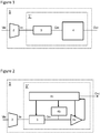
- Figure 1 shows a block diagram of a system 1 for converting an input analogue voltage signal Vin into an output N-bit digital signal Out, the system comprising an input interface circuit 2, a sample and hold circuit 3 and an analogue-to-digital conversion and control circuit 4.
- the input interface circuit 2 is adapted to receive the input analogue voltage signal Vin and comprises voltage-to-current conversion means for converting it into an analogue current signal lin.
- the analogue current signal lin is related to that input analogue voltage signal Vin in the sense that at least one of its characteristics conveys information about the voltage value of the input voltage analogue signal Vin.
- the voltage-to-current (V/I) conversion means could be implemented for example by one or a plurality of trans-conductors and/or variable-gain trans-conductor cells.
- the sample and hold circuit 3 is adapted for receiving and integrating the analogue current signal lin provided by the input interface circuit 2.
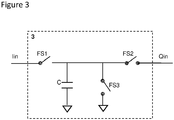
- a schematic and general representation of the sample and hold circuit 3 can be seen in Figure 3 .
- the input analogue current signal lin is converted, in the sample and hold circuit 3, to a charge that is stored in its capacitive means, by integrating that current during a certain time interval on that capacitive means.
- the analogue-to-digital conversion and control circuit 4 comprises successive approximation (SA) conversion means for converting the charge stored in the capacitive means of the S/H circuit 3 into the output N-bit digital signal Out.
- SA conversion steps are based on passive charge-sharing using basically a DAC and a comparator and in which a comparator recognizes the sign of a corresponding differential voltage.
- a general description on how such SA conversion is performed in the charge-domain can be found in international patent application WO 2008/00675 .
- Figure 2 shows another block diagram of an exemplary system 1 for converting an input analogue voltage signal Vin into an output digital signal Out, the system comprising an input interface circuit 2, a sample and hold circuit 3, a comparator 4a, a passive charge-sharing digital-to-analogue converter 4b and an asynchronous SAR logic 4c.
- the system 1 uses the charge that is linearly generated by integrating a V/I converter output current.
- the sign of the charge is determined by activating the comparator and a binary scaled reference charge is added to or subtracted from the total charge by passive charge sharing.
- the described system 1 combines the functionality of an input interface circuit 2, a sample and hold circuit 3 and an analogue-to-digital conversion and control circuit 4, such functionality may be implemented also combining a plurality of independent interconnected devices, each performing one o more functionalities corresponding to the ones disclosed in the present invention.
- a first device or circuit may be used for performing the V/I conversion function and a second device 1' may perform a digital conversion of an input analogue current with the functionality of the sample and hold circuit 3 and the analogue-to digital SAR conversion and control circuit 4.
- the system 1 and/or any individual circuits or devices 1 ' may be implemented in digital CMOS technology.
- Figure 3 is a schematic representation of an exemplary embodiment of a sample and hold circuit 3, basically comprising first, second and third switching means FS1, FS2, FS3 and capacitive means C.
- the switching means could be implemented by any type of switch and the capacitive means by any type of capacitor, such as voltage dependent capacitors, including also MOS capacitors.
- the first switching means FS1 are used to sample the input analogue current signal lin.
- the second switching means FS2 are used to provide a sample of the voltage and charge on the capacitive means C to the analogue-to-digital conversion and control circuit 4 for conversion into the output digital signal Out.
- the third switching means FS3 may be used to reset the charge still remaining in the capacitive means C at the end of the conversion period.
- the transfer function from the input voltage to the sampled charge shows SINC-filtering.
- the input voltage analogue signal Vin reaches a frequency close to Nyquist, the attenuation due to the SINC-filtering increases.
- the quantization noise is flat, spread evenly across the Nyquist bandwidth (f s /2) with a total power of LSB 2 /12.
- Figure 4A illustrates a diagram corresponding to a first operation example of a charge-domain analogue-to-digital conversion and control circuit 4 of a system for analogue-to-digital conversion according to the invention.
- a binary scaled reference charge is added to or subtracted from the total charge by passive charge sharing.
- the analogue-to-digital conversion and control circuit 4 receives an input charge Qin which is a sample of the charge that has been stored in the capacitive means C of the S/H circuit 3 during the current integration period.
- Qin Qin - C0 x 512 Qu
- Cn the n-th most significant bit output code
- Qu the charge unit or the least significant bit (LSB) unit charge.
- the capacitance means C of the sample and hold circuit 3 is reset Rst, so that the residue charge QR is discarded before starting a new conversion.
- Figure 4A illustrates a diagram corresponding to a second operation example of a charge-domain analogue-to-digital conversion and control circuit 4 of a system for analogue-to-digital conversion according to the invention.
- the analogue-to-digital conversion and control circuit 4 does not reset NRst the residue charge QR remaining on the capacitance means C of the sample and hold circuit 3 at the end of the conversion period, so that the residue charge QR, in the next S/H current integration period, will be added (or subtracted, depending on the sign of the charge) to the next input charge Qin.
Landscapes
- Engineering & Computer Science (AREA)
- Theoretical Computer Science (AREA)
- Analogue/Digital Conversion (AREA)
Abstract
The invention relates to a device (1') for converting an input analogue current signal (lin) into an output digital signal (Out), comprising: a sample and hold circuit (3) for providing at least one signal related to the input analogue current signal (lin); an analogue-to digital conversion and control circuit (4) for performing an analogue-to-digital conversion of the at least one related signal at the output of the sample and hold module (3) into said output digital signal (Out); and wherein the sample and hold circuit (3) is adapted for sampling and integrating the analogue current signal (lin) on capacitive means (C); the analogue-to-digital conversion and control circuit (4) comprises successive approximation analogue-to-digital conversion means for converting into the digital output signal (Out), during a conversion period, an input charge value (Qin) present in said capacitive means (C); and the sample and hold circuit (3) and the analogue-to-digital conversion and control circuit (4) being configured to add a residue charge (QR), remaining at the end of a conversion of a previous sample of the input charge value (Qin), to a subsequent sample of input charge value (Qin) to be converted.
The invention also relates to a system (1) for converting an input analogue voltage signal (Vin) into an output digital signal (Out), a method for converting an analogue current signal (lin) into a digital signal (Out), and a method for converting an analogue voltage signal (Vin) into a digital signal (Out).
Description
- The present invention relates to analogue-to-digital conversion and more specifically to a system and method for analogue-to-digital conversion with a noise shaping function.
- Driven by the increasing demand of new-generation product and high-performance applications which require signal processing at ever-lower power usage, analogue-to-digital converters (ADCs) become an important factor for optimizing the overall system power budget of an electronic device.
- As part of the ADC high-performance requirement criteria, noise shaping is an effective technique to achieve high resolution. Its main purpose is to increase the apparent signal to noise ratio of a certain quantized signal by altering the spectral shape of the error that is introduced by quantization and eventually dithering. Document "Noise Shaping Implementation in Two-step/SAR ADC Architectures Based on Delayed Quantization Error", Zhijie Chen et al., 54th IEEE International Midwest Symposium on Circuits and Systems, August 2011, shows an exemplary architecture of a SAR ADC which uses noise shaping, based on delayed analogue quantization error.
- A problem with the state of the art techniques for noise shaping applied to SAR ADCs is that they require a complex methodology and circuitry, which need power and add relevant power consumption for analogue-to-digital conversion systems directed to low power applications.
- The purpose of the invention is to provide an improved device, system and method for analogue-to-digital conversion which performs noise shaping of the quantization noise and requires low power consumption.
- According to one aspect of the present invention, there is provided a device for converting an input analogue current signal into an output digital signal, comprising: a sample and hold circuit for providing at least one signal related to the input analogue current signal; an analogue-to digital conversion and control circuit for performing an analogue-to-digital conversion of the at least one related signal at the output of the sample and hold module into said output digital signal; and wherein the sample and hold circuit is adapted for sampling and integrating the analogue current signal on capacitive means; the analogue-to-digital conversion and control circuit comprises successive approximation analogue-to-digital conversion means for converting into the digital output signal, during a conversion period, an input charge value present in said capacitive means; and the sample and hold circuit and the analogue-to-digital conversion and control circuit being configured to add a residue charge, remaining at the end of a conversion of a previous sample of the input charge value, to a subsequent sample of input charge value to be converted.
- The device for analogue-to-digital conversion according to an embodiment of the invention is able to perform noise shaping of the quantization noise such that the noise is reduced in the used signal bandwidth at lower frequencies and increased at high frequencies. Advantageously, the performance of the device for analogue-to-digital conversion can be thereby increased, at least by achieving an effective resolution higher than the number of bits of the ADC, without increasing the system power consumption. Also advantageous is the fact that noise shaping is achieved without increasing the complexity of the analogue-to-digital conversion system.
- The invention also relates to a system for converting an input analogue voltage signal into an output digital signal, to an integrated circuit, to a method for converting an analogue voltage signal into a digital signal and to a method for converting an analogue current signal into a digital signal.
- Certain objects and advantages of various inventive aspects have been described above. It is to be understood that not necessarily all such objects or advantages may be achieved in accordance with any particular embodiment of the invention. Those skilled in the art will recognize that the invention may be embodied or carried out in a manner that achieves or optimizes one advantage or group of advantages without necessarily achieving other objects or advantages as may be taught or suggested herein. Further embodiments, features, and advantages of the present invention may be described in detail below with reference to the accompanying drawings.
- The accompanying drawings illustrate one or more exemplary embodiment(s) of the present invention and, together with the description, further serve to explain the principles of the invention and to enable a persona skilled in the art to make and use the invention.
-
Figure 1 shows a general block diagram of a first exemplary embodiment of a system for analogue-to-digital conversion according to the present invention. -
Figure 2 shows a general block diagram of a second exemplary embodiment of a system for analogue-to-digital conversion according to the present invention. -
Figure 3 is a schematic representation of an exemplary embodiment of a sample and hold circuit according to the present invention. -
Figure 4A illustrates a diagram corresponding to a first operation example of a charge-domain successive approximation conversion means of a system for analogue-to-digital conversion according to the invention. -
Figure 4B illustrates a diagram corresponding to a second operation example of a charge-domain successive approximation conversion means of a system for analogue-to-digital conversion according to the invention. - In the following, it should be appreciated that in the description of exemplary embodiments of the invention, various features of the invention are sometimes grouped together in a single embodiment, figure, or description thereof for the purpose of streamlining the disclosure and aiding in the understanding of one or more of the various inventive aspects. This is however not to be interpreted as the invention requiring more features than the ones expressly recited in each claim, with each claim standing on its own as a separate embodiment of this invention.
- Furthermore, while some embodiments described herein include some but not other features included in other embodiments, combinations of features of different embodiments are meant to be within the scope of the invention, and form different embodiments, as would be understood by those skilled in the art. In the description of the embodiments, numerous specific details are set forth. However, it is understood that embodiments of the invention may be practiced without these non-essential specific details. In other instances, well-known methods, structures and techniques have not been shown in detail in order not to obscure an understanding of this description.
-
Figure 1 shows a block diagram of asystem 1 for converting an input analogue voltage signal Vin into an output N-bit digital signal Out, the system comprising aninput interface circuit 2, a sample and holdcircuit 3 and an analogue-to-digital conversion andcontrol circuit 4. - The
input interface circuit 2 is adapted to receive the input analogue voltage signal Vin and comprises voltage-to-current conversion means for converting it into an analogue current signal lin. The analogue current signal lin is related to that input analogue voltage signal Vin in the sense that at least one of its characteristics conveys information about the voltage value of the input voltage analogue signal Vin. The voltage-to-current (V/I) conversion means could be implemented for example by one or a plurality of trans-conductors and/or variable-gain trans-conductor cells. - The sample and
hold circuit 3 is adapted for receiving and integrating the analogue current signal lin provided by theinput interface circuit 2. A schematic and general representation of the sample andhold circuit 3 can be seen inFigure 3 . - According to the invention, the input analogue current signal lin is converted, in the sample and hold
circuit 3, to a charge that is stored in its capacitive means, by integrating that current during a certain time interval on that capacitive means. - The analogue-to-digital conversion and
control circuit 4 comprises successive approximation (SA) conversion means for converting the charge stored in the capacitive means of the S/H circuit 3 into the output N-bit digital signal Out. The SA conversion steps are based on passive charge-sharing using basically a DAC and a comparator and in which a comparator recognizes the sign of a corresponding differential voltage. A general description on how such SA conversion is performed in the charge-domain can be found in international patent applicationWO 2008/00675 -
Figure 2 shows another block diagram of anexemplary system 1 for converting an input analogue voltage signal Vin into an output digital signal Out, the system comprising aninput interface circuit 2, a sample and holdcircuit 3, acomparator 4a, a passive charge-sharing digital-to-analogue converter 4b and anasynchronous SAR logic 4c. - According to an embodiment of the invention, the
system 1 uses the charge that is linearly generated by integrating a V/I converter output current. In each of the steps of the successive approximation controller, the sign of the charge is determined by activating the comparator and a binary scaled reference charge is added to or subtracted from the total charge by passive charge sharing. - It shall be understood that although the described
system 1 according to an embodiment of the invention combines the functionality of aninput interface circuit 2, a sample and holdcircuit 3 and an analogue-to-digital conversion andcontrol circuit 4, such functionality may be implemented also combining a plurality of independent interconnected devices, each performing one o more functionalities corresponding to the ones disclosed in the present invention. For example, a first device or circuit may be used for performing the V/I conversion function and a second device 1' may perform a digital conversion of an input analogue current with the functionality of the sample and holdcircuit 3 and the analogue-to digital SAR conversion andcontrol circuit 4. - The
system 1 and/or any individual circuits or devices 1' may be implemented in digital CMOS technology. -
Figure 3 is a schematic representation of an exemplary embodiment of a sample and holdcircuit 3, basically comprising first, second and third switching means FS1, FS2, FS3 and capacitive means C. The switching means could be implemented by any type of switch and the capacitive means by any type of capacitor, such as voltage dependent capacitors, including also MOS capacitors. - The first switching means FS1 are used to sample the input analogue current signal lin. The second switching means FS2 are used to provide a sample of the voltage and charge on the capacitive means C to the analogue-to-digital conversion and
control circuit 4 for conversion into the output digital signal Out. The third switching means FS3 may be used to reset the charge still remaining in the capacitive means C at the end of the conversion period. - The transfer function from the input voltage to the sampled charge, in this case, shows SINC-filtering. As the input voltage analogue signal Vin reaches a frequency close to Nyquist, the attenuation due to the SINC-filtering increases. The quantization noise is flat, spread evenly across the Nyquist bandwidth (fs/2) with a total power of LSB2/12.
-
Figure 4A illustrates a diagram corresponding to a first operation example of a charge-domain analogue-to-digital conversion andcontrol circuit 4 of a system for analogue-to-digital conversion according to the invention. - According to SAR operation, in each of the steps of the successive approximation controller COMP1 to COMPN, a binary scaled reference charge is added to or subtracted from the total charge by passive charge sharing. For example, before the first comparison is performed, the analogue-to-digital conversion and
control circuit 4 receives an input charge Qin which is a sample of the charge that has been stored in the capacitive means C of the S/H circuit 3 during the current integration period. After first comparison COMP1 the total charge remaining is calculated as Q1 = Qin - C0 x 512 Qu, where Cn is the n-th most significant bit output code and Qu is the charge unit or the least significant bit (LSB) unit charge. After second comparison COMP2 the total charge remaining is calculated as Q2 = Qin - C0 x 512 Qu - C1 x 256 Qu. After third comparison COMP3 the total charge remaining is calculated as Q3 = Qin - C0 x 512 Qu - C1 x 256 Qu - C2 x 128 Qu, and so successively until the end of conversion COMPN, in which the remaining charge is the difference between the input charge Qin and the digital (quantized) estimation of that input, which is called the residue charge QR. It shall be noted that the sign of the remaining charge may be positive or negative, and while in some steps it may be added, in others it may be subtracted. - According to an embodiment of the invention, before sampling the next input charge Qin on the capacitance means C of the sample and hold
circuit 3 the capacitance means C of the sample and holdcircuit 3 is reset Rst, so that the residue charge QR is discarded before starting a new conversion. -
Figure 4A illustrates a diagram corresponding to a second operation example of a charge-domain analogue-to-digital conversion andcontrol circuit 4 of a system for analogue-to-digital conversion according to the invention. Instead of discarding the residue charge QR, according to an embodiment of the invention, the analogue-to-digital conversion andcontrol circuit 4 does not reset NRst the residue charge QR remaining on the capacitance means C of the sample and holdcircuit 3 at the end of the conversion period, so that the residue charge QR, in the next S/H current integration period, will be added (or subtracted, depending on the sign of the charge) to the next input charge Qin. - The remaining errors, i.e. the residue, add-up and this results in a shaping of the quantization noise towards higher frequencies, such that in the lower part of the input spectrum, the quantization noise floor is reduced. Advantageously an effective resolution higher than the number of bits of the ADC is obtained.
Claims (5)
- A device (1') for converting an input analogue current signal (lin) into an output digital signal (Out), comprising:- a sample and hold circuit (3) for providing at least one signal related to the input analogue current signal (lin);- an analogue-to digital conversion and control circuit (4) for performing an analogue-to-digital conversion of the at least one related signal at the output of the sample and hold module (3) into said output digital signal (Out); andcharacterized in that- the sample and hold circuit (3) is adapted for sampling and integrating the analogue current signal (lin) on capacitive means (C);- the analogue-to-digital conversion and control circuit (4) comprises successive approximation analogue-to-digital conversion means for converting into the digital output signal (Out), during a conversion period, an input charge value (Qin) present in said capacitive means (C); and- the sample and hold circuit (3) and the analogue-to-digital conversion and control circuit (4) being configured to add a residue charge (QR), remaining at the end of a conversion of a previous sample of the input charge value (Qin), to a subsequent sample of input charge value (Qin) to be converted.
- A system (1) for converting an input analogue voltage signal (Vin) into an output digital signal (Out), comprising:- an input interface circuit (2) for receiving said analogue voltage signal (Vin) and comprising voltage-to-current conversion means for converting the analogue voltage signal (Vin) into an analogue current signal (lin); and- a device (1') according to claim 1 for converting the analogue current signal (lin) into the output digital signal (Out).
- An integrated circuit comprising a system (1) for converting an input analogue voltage signal (Vin) into an output digital signal (Out) according to claim 2 or a device (1') for converting an input analogue current signal (lin) into an output digital signal (Out) according to claim 1.
- A method for converting an analogue current signal (lin) into a digital signal (Out), comprising:- sampling and integrating the analogue current signal (lin) on capacitive means (C);- providing to a charge-domain analogue-to-digital converting means (4) a sample of an input charge value (Qin) stored in said capacitive means (C) and said charge-domain analogue-to-digital converting means (4) converting, during a conversion period, said input charge value (Qin) into the digital signal (Out); and- adding a residue charge (QR), remaining at the end of a conversion of a previous sample of the input charge value (Qin), to a subsequent sample of the input charge value (Qin) to be converted.
- A method for converting an analogue voltage signal (Vin) into a digital signal (Out), comprising:- converting the analogue voltage signal (Vin) into an analogue current signal (lin) related to said analogue voltage signal (Vin); and- converting the analogue current signal (lin) into the digital signal (Out) according to the method of claim 4.
Priority Applications (1)
| Application Number | Priority Date | Filing Date | Title |
|---|---|---|---|
| EP12156092.4A EP2629426A1 (en) | 2012-02-17 | 2012-02-17 | Device, system and method for analogue-to-digital conversion with noise shaping function |
Applications Claiming Priority (1)
| Application Number | Priority Date | Filing Date | Title |
|---|---|---|---|
| EP12156092.4A EP2629426A1 (en) | 2012-02-17 | 2012-02-17 | Device, system and method for analogue-to-digital conversion with noise shaping function |
Publications (1)
| Publication Number | Publication Date |
|---|---|
| EP2629426A1 true EP2629426A1 (en) | 2013-08-21 |
Family
ID=45656124
Family Applications (1)
| Application Number | Title | Priority Date | Filing Date |
|---|---|---|---|
| EP12156092.4A Withdrawn EP2629426A1 (en) | 2012-02-17 | 2012-02-17 | Device, system and method for analogue-to-digital conversion with noise shaping function |
Country Status (1)
| Country | Link |
|---|---|
| EP (1) | EP2629426A1 (en) |
Cited By (5)
| Publication number | Priority date | Publication date | Assignee | Title |
|---|---|---|---|---|
| CN109728812A (en) * | 2017-10-30 | 2019-05-07 | 亚德诺半导体无限责任公司 | Noise shaping analog-digital converter |
| CN110622422A (en) * | 2017-03-10 | 2019-12-27 | 赛灵思公司 | SAR ADC with programmable resolution |
| CN111049526A (en) * | 2018-10-12 | 2020-04-21 | 联发科技股份有限公司 | Analog-to-digital converter |
| CN111435836A (en) * | 2019-01-11 | 2020-07-21 | 瑞昱半导体股份有限公司 | Analog to digital conversion device |
| CN113691275A (en) * | 2021-09-09 | 2021-11-23 | 苏州汇川控制技术有限公司 | Digital signal transmission circuit and digital signal transmission device |
Citations (2)
| Publication number | Priority date | Publication date | Assignee | Title |
|---|---|---|---|---|
| WO2008000675A2 (en) | 2006-06-30 | 2008-01-03 | Saab Ab | Dispenser arrangement for discharging countermeasure means |
| WO2008142486A1 (en) * | 2007-05-18 | 2008-11-27 | Nokia Corporation | Analogue-to-digital converter |
-
2012
- 2012-02-17 EP EP12156092.4A patent/EP2629426A1/en not_active Withdrawn
Patent Citations (2)
| Publication number | Priority date | Publication date | Assignee | Title |
|---|---|---|---|---|
| WO2008000675A2 (en) | 2006-06-30 | 2008-01-03 | Saab Ab | Dispenser arrangement for discharging countermeasure means |
| WO2008142486A1 (en) * | 2007-05-18 | 2008-11-27 | Nokia Corporation | Analogue-to-digital converter |
Non-Patent Citations (3)
| Title |
|---|
| CARLEY L R ET AL: "HIGH-SPEED LOW-POWER INTEGRATING CMOS SAMPLE-AND-HOLD AMPLIFIER ARCHITECTURE", PROCEEDINGS OF THE CUSTOM INTEGRATED CIRCUITS CONFERENCE. SANTA CLARA, MAY 1 - 4, 1995; [PROCEEDINGS OF THE CUSTOM INTEGRATED CIRCUITS CONFERENCE], NEW YORK, IEEE, US, vol. CONF. 17, 1 May 1995 (1995-05-01), pages 543 - 546, XP000536863, ISBN: 978-0-7803-2585-2, DOI: 10.1109/CICC.1995.518242 * |
| KIM K S ET AL: "nth-order multi-bit Î GBP Î ADC using SAR quantiser", THE INSTITUTION OF ENGINEERING AND TECHNOLOGY. JOURNAL,, vol. 46, no. 19, 16 September 2010 (2010-09-16), pages 1315 - 1316, XP006036931, ISSN: 1350-911X, DOI: 10.1049/EL:20101554 * |
| ZHIJIE CHEN ET AL.: "Noise Shaping Implementation in Two-step/SAR ADC Architectures Based on Delayed Quantization Error", 54TH IEEE INTERNATIONAL MIDWEST SYMPOSIUM ON CIRCUITS AND SYSTEMS, August 2011 (2011-08-01) |
Cited By (8)
| Publication number | Priority date | Publication date | Assignee | Title |
|---|---|---|---|---|
| CN110622422A (en) * | 2017-03-10 | 2019-12-27 | 赛灵思公司 | SAR ADC with programmable resolution |
| CN110622422B (en) * | 2017-03-10 | 2024-03-29 | 赛灵思公司 | Resolution programmable SAR ADC |
| CN109728812A (en) * | 2017-10-30 | 2019-05-07 | 亚德诺半导体无限责任公司 | Noise shaping analog-digital converter |
| CN111049526A (en) * | 2018-10-12 | 2020-04-21 | 联发科技股份有限公司 | Analog-to-digital converter |
| CN111049526B (en) * | 2018-10-12 | 2023-11-03 | 联发科技股份有限公司 | analog to digital converter |
| CN111435836A (en) * | 2019-01-11 | 2020-07-21 | 瑞昱半导体股份有限公司 | Analog to digital conversion device |
| CN111435836B (en) * | 2019-01-11 | 2023-06-20 | 瑞昱半导体股份有限公司 | Analog-to-digital conversion device |
| CN113691275A (en) * | 2021-09-09 | 2021-11-23 | 苏州汇川控制技术有限公司 | Digital signal transmission circuit and digital signal transmission device |
Similar Documents
| Publication | Publication Date | Title |
|---|---|---|
| US10790843B2 (en) | Analog-to-digital converter device | |
| US8947286B2 (en) | Analog/digital converter | |
| US10778242B2 (en) | Analog-to-digital converter device | |
| US7551114B2 (en) | Reducing power consumption in the early stages of a pipeline sub-ADC used in a time-interleaved ADC | |
| KR101122462B1 (en) | Successive approxiamation analog/digtal converter and time-interleaved successive approxiamation analog/digtal converter | |
| US20180183450A1 (en) | Interleaving successive approximation analog-to-digital converter with noise shaping | |
| EP2055006B1 (en) | Analog-to-digital conversion using asynchronous current-mode cyclic comparison | |
| EP2053748A1 (en) | Analogue-to-digital converter and method for using the same | |
| WO2017006297A2 (en) | Hybrid charge-sharing charge-redistribution dac for successive approximation analog-to-digital converters | |
| KR20060052937A (en) | Space Efficient Low Power Periodic A / D Converter | |
| KR20190071536A (en) | Successive approximation register analog digital converter and operating method thereof | |
| US8842029B2 (en) | Area-efficiency delta modulator for quantizing an analog signal | |
| KR101603892B1 (en) | Successive approxiamtion analog digital converter and converting method | |
| CN102916701B (en) | Multiplying digital-to-analog converter and production line analog-digital converter | |
| CN104158545A (en) | Successive approximation register analog-to-digital converter based on voltage-controlled oscillator quantization | |
| CN112187265A (en) | Mixed type analog-digital converter and signal transceiver for electric power special communication network | |
| US20090295609A1 (en) | System and method for reducing power dissipation in an analog to digital converter | |
| KR101878593B1 (en) | Analog to digital converter and operating method thereof | |
| CN117879603A (en) | A low-power digital front-end self-calibration method for SAR ADC | |
| EP2577407B1 (en) | Method and apparatus for conversion of voltage value to digital word | |
| KR101986699B1 (en) | Successive approximation register analog digital converter and operating method thereof | |
| CN116137530B (en) | Time-interleaved analog-to-digital converter | |
| Atchaya et al. | Design of High Speed Time–Interleaved SAR Analog to Digital Converter | |
| CN113556127B (en) | Digital slope type analog-digital converter device and signal conversion method | |
| US8922417B2 (en) | Method and apparatus for conversion of portion of electric charge to digital word |
Legal Events
| Date | Code | Title | Description |
|---|---|---|---|
| PUAI | Public reference made under article 153(3) epc to a published international application that has entered the european phase |
Free format text: ORIGINAL CODE: 0009012 |
|
| AK | Designated contracting states |
Kind code of ref document: A1 Designated state(s): AL AT BE BG CH CY CZ DE DK EE ES FI FR GB GR HR HU IE IS IT LI LT LU LV MC MK MT NL NO PL PT RO RS SE SI SK SM TR |
|
| AX | Request for extension of the european patent |
Extension state: BA ME |
|
| STAA | Information on the status of an ep patent application or granted ep patent |
Free format text: STATUS: THE APPLICATION IS DEEMED TO BE WITHDRAWN |
|
| 18D | Application deemed to be withdrawn |
Effective date: 20140222 |