EP2629409A1 - Regulator, battery charging apparatus, and battery charging system - Google Patents
Regulator, battery charging apparatus, and battery charging system Download PDFInfo
- Publication number
- EP2629409A1 EP2629409A1 EP11832477.1A EP11832477A EP2629409A1 EP 2629409 A1 EP2629409 A1 EP 2629409A1 EP 11832477 A EP11832477 A EP 11832477A EP 2629409 A1 EP2629409 A1 EP 2629409A1
- Authority
- EP
- European Patent Office
- Prior art keywords
- battery
- terminal
- phase
- current
- semiconductor devices
- Prior art date
- Legal status (The legal status is an assumption and is not a legal conclusion. Google has not performed a legal analysis and makes no representation as to the accuracy of the status listed.)
- Withdrawn
Links
Images


Classifications
-
- H—ELECTRICITY
- H02—GENERATION; CONVERSION OR DISTRIBUTION OF ELECTRIC POWER
- H02J—ELECTRIC POWER NETWORKS; CIRCUIT ARRANGEMENTS OR SYSTEMS FOR SUPPLYING OR DISTRIBUTING ELECTRIC POWER; SYSTEMS FOR STORING ELECTRIC ENERGY
- H02J7/00—Circuit arrangements for charging or discharging batteries or for supplying loads from batteries
- H02J7/90—Regulation of charging or discharging current or voltage
- H02J7/933—Regulation of charging or discharging current or voltage the cycle being controlled or terminated in response to electric parameters
-
- H—ELECTRICITY
- H02—GENERATION; CONVERSION OR DISTRIBUTION OF ELECTRIC POWER
- H02J—ELECTRIC POWER NETWORKS; CIRCUIT ARRANGEMENTS OR SYSTEMS FOR SUPPLYING OR DISTRIBUTING ELECTRIC POWER; SYSTEMS FOR STORING ELECTRIC ENERGY
- H02J7/00—Circuit arrangements for charging or discharging batteries or for supplying loads from batteries
-
- H—ELECTRICITY
- H02—GENERATION; CONVERSION OR DISTRIBUTION OF ELECTRIC POWER
- H02J—ELECTRIC POWER NETWORKS; CIRCUIT ARRANGEMENTS OR SYSTEMS FOR SUPPLYING OR DISTRIBUTING ELECTRIC POWER; SYSTEMS FOR STORING ELECTRIC ENERGY
- H02J7/00—Circuit arrangements for charging or discharging batteries or for supplying loads from batteries
- H02J7/02—Circuit arrangements for charging or discharging batteries or for supplying loads from batteries for charging batteries from AC mains by converters
- H02J7/04—Regulation of charging current or voltage
- H02J7/06—Regulation of charging current or voltage using discharge tubes or semiconductor devices
-
- H—ELECTRICITY
- H02—GENERATION; CONVERSION OR DISTRIBUTION OF ELECTRIC POWER
- H02J—ELECTRIC POWER NETWORKS; CIRCUIT ARRANGEMENTS OR SYSTEMS FOR SUPPLYING OR DISTRIBUTING ELECTRIC POWER; SYSTEMS FOR STORING ELECTRIC ENERGY
- H02J7/00—Circuit arrangements for charging or discharging batteries or for supplying loads from batteries
- H02J7/14—Circuit arrangements for charging or discharging batteries or for supplying loads from batteries for charging batteries from dynamo-electric generators driven at varying speed, e.g. on vehicle
- H02J7/1415—Circuit arrangements for charging or discharging batteries or for supplying loads from batteries for charging batteries from dynamo-electric generators driven at varying speed, e.g. on vehicle with a generator driven by a prime mover other than the motor of a vehicle
-
- H—ELECTRICITY
- H02—GENERATION; CONVERSION OR DISTRIBUTION OF ELECTRIC POWER
- H02J—ELECTRIC POWER NETWORKS; CIRCUIT ARRANGEMENTS OR SYSTEMS FOR SUPPLYING OR DISTRIBUTING ELECTRIC POWER; SYSTEMS FOR STORING ELECTRIC ENERGY
- H02J7/00—Circuit arrangements for charging or discharging batteries or for supplying loads from batteries
- H02J7/14—Circuit arrangements for charging or discharging batteries or for supplying loads from batteries for charging batteries from dynamo-electric generators driven at varying speed, e.g. on vehicle
- H02J7/1469—Regulation of the charging current or voltage otherwise than by variation of field
- H02J7/1492—Regulation of the charging current or voltage otherwise than by variation of field by means of controlling devices between the generator output and the battery
-
- H—ELECTRICITY
- H02—GENERATION; CONVERSION OR DISTRIBUTION OF ELECTRIC POWER
- H02M—APPARATUS FOR CONVERSION BETWEEN AC AND AC, BETWEEN AC AND DC, OR BETWEEN DC AND DC, AND FOR USE WITH MAINS OR SIMILAR POWER SUPPLY SYSTEMS; CONVERSION OF DC OR AC INPUT POWER INTO SURGE OUTPUT POWER; CONTROL OR REGULATION THEREOF
- H02M7/00—Conversion of AC power input into DC power output; Conversion of DC power input into AC power output
- H02M7/02—Conversion of AC power input into DC power output without possibility of reversal
- H02M7/04—Conversion of AC power input into DC power output without possibility of reversal by static converters
- H02M7/06—Conversion of AC power input into DC power output without possibility of reversal by static converters using discharge tubes without control electrode or semiconductor devices without control electrode
-
- H—ELECTRICITY
- H02—GENERATION; CONVERSION OR DISTRIBUTION OF ELECTRIC POWER
- H02J—ELECTRIC POWER NETWORKS; CIRCUIT ARRANGEMENTS OR SYSTEMS FOR SUPPLYING OR DISTRIBUTING ELECTRIC POWER; SYSTEMS FOR STORING ELECTRIC ENERGY
- H02J2207/00—Details of circuit arrangements for charging or discharging batteries or supplying loads from batteries
- H02J2207/20—Charging or discharging characterised by the power electronics converter
-
- H—ELECTRICITY
- H02—GENERATION; CONVERSION OR DISTRIBUTION OF ELECTRIC POWER
- H02M—APPARATUS FOR CONVERSION BETWEEN AC AND AC, BETWEEN AC AND DC, OR BETWEEN DC AND DC, AND FOR USE WITH MAINS OR SIMILAR POWER SUPPLY SYSTEMS; CONVERSION OF DC OR AC INPUT POWER INTO SURGE OUTPUT POWER; CONTROL OR REGULATION THEREOF
- H02M1/00—Details of apparatus for conversion
- H02M1/0083—Converters characterised by their input or output configuration
- H02M1/0085—Partially controlled bridges
Definitions
- the present invention relates to a regulator that control charging of a battery by a three-phase alternating-current generator, a battery charging apparatus and a battery charging system.
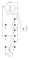
- Figure 4 is a diagram showing an example of a configuration of a conventional battery charging system 1000A.
- a regulator in the conventional battery charging system 1000A makes a rectifying circuit, which is composed of six diodes “D1" to "D6", rectify the output current of a three-phase alternating-current generator 101 and charges a battery "B" with the rectified current while charging the battery.
- a controller "CON" of the regulator detects the battery voltage and turns on thyristors "S1 to “S3", which are opposite in polarity to and connected in parallel with the diodes "D4" to “D6”, respectively, by passing a driving current through the thyristors "S1" to S3".
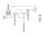
- Figure 5 is a circuit diagram showing an example of a circuit configuration of the first to third thyristors "S1" to "S3" of the battery charging apparatus shown in Figure 4 .
- the heat quantity is the product of the generator short-circuit current and the on-voltage of the thyristors "S1" to “S3".
- the on-voltage of the thyristors "S1" to “S3” is about 1.3 V (the sum of the base-emitter voltage "Vbe” of the upper transistor and the collector-emitter voltage "Vce” of the lower transistor), for example. Therefore, if the generator short-circuit current is 10 A, 13 W of heat is generated.
- the thyristor since the thyristor has a self-holding characteristic, in order to turn off the thyristors "S1" to “S3" that have once been turned on, a certain turn-off time is required to allow the current flowing between the anode and the cathode of the thyristors "S1" to “S3” to be equal to or smaller than a holding current.
- the output of the three-phase alternating-current generator 101 has a high frequency, and the certain turn-off time cannot be provided to allow the current flowing between the anode and the cathode of the thyristors "S1" to "S3" to be equal to or smaller than the holding current. In this case, the thyristors are not turned off.
- the regulator according to the prior art has high power loss and cannot appropriately control charging of the battery when the output of the three-phase alternating-current generator is high.
- a regulator according to one aspect of the invention is a regulator that controls charging of a battery by a three-phase alternating-current generator, comprising:
- each of the first to third semiconductor devices has:
- the regulator may further comprise first to third resistive elements that are connected between the positive side of the battery and the third terminals of the first to third semiconductor devices, respectively.
- the regulator may further comprise first to third switching circuits that are connected between the positive side of the battery and the third terminals of the first to third semiconductor devices, respectively, are controlled by the controller, are turned on to connect the positive side of the battery and the third terminals of the first to third semiconductor devices to each other, respectively, and turned off to disconnect the positive side of the battery and the third terminals of the first to third semiconductor devices from each other, respectively, and the controller stops supplying the control signals to the first terminals and turning off the first to third switching circuits when the charging voltage for the battery is lower than the threshold voltage.
- the regulator may further comprise first to third switching circuits that are connected between the first and second terminals of the first to third semiconductor devices, respectively, are controlled by the controller, are turned on to connect the first and second terminals of the first to third semiconductor devices to each other, respectively, and turned off to disconnect the first and second terminals of the first to third semiconductor devices from each other, respectively, and the controller stops supplying the control signals to the first terminals and turning off the first to third switching circuits when the charging voltage for the battery is lower than the threshold voltage.
- the first bipolar transistor is an NPN type bipolar transistor
- the second bipolar transistor is a PNP type bipolar transistor
- the rectifying circuit has:
- the first to third switching circuits may be transistors.
- the controller may output the control signals only for a certain period.
- control signals may be pulse waves.
- the negative side of the battery may be grounded.
- a battery charging apparatus is a battery charging apparatus that charges a battery, comprises:
- a battery charging system is a battery charging system that charges a battery, comprising:
- a regulator makes second transistors in first to third semiconductor devices operate by passing a current smaller than a generator short-circuiting current, rather than the generator short-circuiting current, between the emitters and the bases of the second transistors.
- the Joule heat of the second transistors (the product of the base-emitter voltage "Vbe" of the second transistor and the current flowing between the emitter and the base of the second transistor) is reduced, the power loss is reduced compared with the prior art described above, and the size of the radiator fin can be reduced.
- the first to third semiconductor devices can be turned off with higher reliability by turning off the switching circuits to forcedly eliminate the positive feedback current.
- the regulator according to the aspect of the present invention can reduce the power loss and more appropriately control charging of the battery.
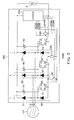
- Figure 1 is a diagram showing an example of a configuration of a battery charging system 1000 according to an embodiment 1 of the present invention, which is an aspect of the present invention.
- Figure 2 is a circuit diagram showing an example of a circuit configuration of first to third semiconductor devices "T1" to "T3" of a battery charging apparatus 100 shown in Figure 1 .
- the battery charging system 1000 that charges a battery has a battery "B", a three-phase alternating-current generator 101, and a regulator 100. Note that the three-phase alternating-current generator 101 and the regulator 100 form the battery charging apparatus that charges the battery "B".
- the battery “B” has a positive terminal (positive side) and a negative terminal (negative side) and is capable of being charged and discharging through the terminals.
- the negative side of the battery is grounded.
- the three-phase alternating-current generator 101 is configured to generate an alternating-current voltage for charging the battery "B” and supply the alternating-current voltage through output terminals of the three phases (U phase, V phase, and W phase).
- the regulator 100 is configured to control charging of the battery "B" by the three-phase alternating-current generator 101.
- the regulator 100 has a rectifying circuit 1, a first semiconductor device “T1”, a second semiconductor device “T2”, a third semiconductor device “T3”, a first resistive element “R1”, a second resistive element “R2”, a third resistive element “R3”, a first switching circuit “SW1”, a second switching circuit “SW2”, a third switching circuit “SW3”, and a controller "CON".
- the rectifying circuit 1 is configured to rectify an alternating current output from the output terminal of each phase (U phase, V phase, W phase) of the three-phase alternating-current generator 101 and pass a charging current to the battery "B".
- the rectifying circuit 1 has a first diode "D1", a second diode “D2”, a third diode “D3”, a fourth diode “D4", a fifth diode “D5", and a sixth diode “D6", for example.
- the first diode “D1" is connected to the output terminal of the U phase of the three-phase alternating-current generator 101 at the anode thereof and to the positive side of the battery "B" at the cathode thereof.
- the second diode “D2" is connected to the output terminal of the V phase of the three-phase alternating-current generator 101 at the anode thereof and to the positive side of the battery "B" at the cathode thereof.
- the third diode “D3" is connected to the output terminal of the W phase of the three-phase alternating-current generator 101 at the anode thereof and to the positive side of the battery "B" at the cathode thereof.
- the fourth diode "D4" is connected to the output terminal of the U phase of the three-phase alternating-current generator 101 at the cathode thereof and to the negative side of the battery "B" at the anode thereof.
- the fifth diode "D5" is connected to the output terminal of the V phase of the three-phase alternating-current generator 101 at the cathode thereof and to the negative side of the battery "B" at the anode thereof.
- the sixth diode “D6" is connected to the output terminal of the W phase of the three-phase alternating-current generator 101 at the cathode thereof and to the negative side of the battery "B" at the anode thereof.
- the first semiconductor device “T1” has a first terminal “x1” to which a control signal “SCON1" is input, a second terminal “x2” connected to the negative side of the battery “B", a third terminal “x3” connected to the positive side of the battery “B”, and a fourth terminal “x4" connected to the output terminal of the U phase of the three-phase alternating-current generator 101.
- the second semiconductor device “T2” has a first terminal “x1” to which a control signal "SCON2" is input, a second terminal “x2” connected to the negative side of the battery “B", a third terminal “x3” connected to the positive side of the battery “B”, and a fourth terminal “x4" connected to the output terminal of the V phase of the three-phase alternating-current generator 101.
- the third semiconductor device “T3” has a first terminal “x1” to which a control signal "SCON3" is input, a second terminal “x2" connected to the negative side of the battery “B", a third terminal “x3” connected to the positive side of the battery “B”, and a fourth terminal “x4" connected to the output terminal of the W phase of the three-phase alternating-current generator 101.
- each of the first to third semiconductor devices "T1" to “T3” has a first bipolar transistor of a first conductivity type (NPN type bipolar transistor) "Tr1" and a second bipolar transistor of a second conductivity type (PNP type bipolar transistor).
- NPN type bipolar transistor first conductivity type bipolar transistor
- PNP type bipolar transistor second conductivity type bipolar transistor
- the first bipolar transistor "Tr1" is connected to the first terminal "x1" at the base thereof, to the second terminal "x2" at the emitter thereof, and to the fourth terminal "x4" at the collector thereof.
- the second bipolar transistor is connected to the fourth terminal "x4" at the base thereof, to the first terminal "x1" at the collector thereof, and to the third terminal "x3" at the emitter thereof.
- the first to third semiconductor devices “T1" to “T3” are configured to pass a current between the fourth terminal “x4" and the second terminal “x2" when a current of a prescribed value or larger flows between the third terminal “x3” and the second terminal “x2" in response to input of the control signals "SCON1" to “SCON3", respectively. Furthermore, the first to third semiconductor devices “T1” to “T3” are configured to continue passing a current between the fourth terminal "x4" and the second terminal "x2" while a current continues flowing between the third terminal "x3" and the second terminal "x2".
- the first to third semiconductor devices "T1" to “T3” cut off the current between the fourth terminal "x4" and the second terminal "x2" when input of the control signals "SCON1" to “SCON3" is stopped, and the current from the third terminal "x3" is cut off.
- the first resistive element "R1" is connected between the positive side of the battery "B” and the third terminal "x3" of the first semiconductor device "T1".
- the second resistive element "R2" is connected between the positive side of the battery "B” and the third terminal "x3" of the second semiconductor device "T2".
- the third resistive element "R3" is connected between the positive side of the battery "B” and the third terminal "x3" of the third semiconductor device "T3".
- the first switching circuit “SW1” is connected between the positive side of the battery “B” and the third terminal “x3" of the first semiconductor device “T1".
- the first switching circuit “SW1” is controlled by a control signal “SCON4" from the controller "CON" and is turned on to connect the positive side of the battery "B” and the third terminal “x3” of the first semiconductor device “T1” to each other and is turned off to disconnect the positive side of the battery "B” and the third terminal "x3" of the first semiconductor device “T1" from each other.
- the second switching circuit “SW2" is connected between the positive side of the battery “B” and the third terminal “x3" of the second semiconductor device “T2".
- the second switching circuit “SW2” is controlled by a control signal "SCON5" from the controller "CON" and is turned on to connect the positive side of the battery "B” and the third terminal “x3” of the second semiconductor device “T2” to each other and is turned off to disconnect the positive side of the battery "B” and the third terminal "x3" of the second semiconductor device “T2" from each other.
- the third switching circuit “SW3” is connected between the positive side of the battery “B” and the third terminal “x3” of the third semiconductor device “T3".
- the third switching circuit “SW3” is controlled by a control signal "SCON6" from the controller "CON" and is turned on to connect the positive side of the battery "B” and the third terminal “x3” of the third semiconductor device “T3” to each other and is turned off to disconnect the positive side of the battery "B” and the third terminal "x3" of the third semiconductor device “T3” from each other.
- the first to third switching circuits "SW1" to “SW3” are each formed by a bipolar transistor (MOS transistor) that is connected between the positive side of the battery "B” and the third terminal “x3" and receives the control signal "SCON4" to "SCON6" at the base (gate) thereof, for example.
- MOS transistor bipolar transistor
- the controller "CON” is configured to detect a charging voltage for the battery “B” and control the first to third semiconductor devices “T1" to “T3” by outputting the control signals “SCON1” to “SCON3” based on the detection result.
- the controller “CON” outputs the control signals “SCON1” to “SCON3” only for a certain period. Therefore, the control signals “SCON1” to “SCON3” are pulse waves, for example.
- controller "CON" is configured to detect the charging voltage for the battery “B” and control the first to third switching circuits “SW1" to “SW3” by outputting the control signals "SCON4" to "SCON6” based on the detection result.
- the controller "CON" when the charging voltage for the battery “B" is equal to or higher than a preset threshold voltage (an overcharge voltage, for example), the controller "CON" outputs the control signals "SCON1" to "SCON3" to the first terminals "x1" of the first to third semiconductor devices “T1" to “T3", thereby connecting the second terminals "x2" and the fourth terminals "x4" of the first to third semiconductor devices “T1" to “T3” to each other.
- a preset threshold voltage an overcharge voltage, for example
- the controller "CON” stops supplying the control signals "SCON1" to “SCON3" to the first terminals “x1" of the first to third semiconductor devices “T1" to “T3” and outputs the fourth to sixth control signals "SCON4" to "SCON6” to the first to third switching circuits "SW1" to “SW3", thereby temporarily turning off the first to third switching circuits "SW1” to "SW3” (otherwise, the first to third switching circuits "SW1" to “SW3” are in the on state).
- the three-phase alternating-current generator 101 generates an alternating-current voltage for charging the battery "B” and supplies the alternating-current voltage from the output terminal of each phase (U phase, V phase and W phase). Then, the rectifying circuit 1 in the regulator 100 rectifies the alternating current output from the output terminal of each phase (U phase, V phase and W phase) of the three-phase alternating-current generator 101 and passes a charging current to the battery "B". This causes the charging voltage for the battery "B" to rise.
- the controller "CON" outputs the control signals "SCON1" to "SCON3" to the first terminals "x1" of the first to third semiconductor devices “T1" to “T3", thereby connecting the second terminals "x2" and the fourth terminals "x4" of the first to third semiconductor devices "T1" to “T3” to each other.
- a preset threshold voltage an overcharge voltage, for example
- the controller "CON” stops supplying the control signals "SCON1" to “SCON3" to the first terminals “x1" of the first to third semiconductor devices “x1" to “T3” and outputs the fourth to sixth control signals "SCON4" to "SCON6” to the first to third switching circuits "SW1" to “SW3", thereby temporarily turning off the first to third switching circuits "SW1" to "SW3".
- the charging voltage for the battery “B” is maintained in the vicinity of the threshold voltage by the battery charging system 1000 repeating the operation described above.
- the regulator 100 makes the second transistors "Tr2" of the first to third semiconductor devices “T1" to “T3” operate by passing a current smaller than the generator short-circuiting current, rather than the generator short-circuiting current, between the emitters and the bases of the second transistors "Tr2".
- the Joule heat of the second transistors "Tr2" (the product of the base-emitter voltage "Vbe” of the second transistor and the current flowing between the emitter and the base of the second transistor), the power loss is reduced compared with the prior art described above, and the size of the radiator fin can be reduced.
- the first to third switching circuits "SW1" to “SW3” are turned off, the first to third semiconductor devices “T1" to “T3” can be turned off with higher reliability.
- the regulator according to this embodiment can more appropriately control charging of the battery while reducing the power loss.
- the first to third switching circuits "SW1" to “SW3” can be arranged in a different way as far as the first to third semiconductor devices “T1" to “T3” can be turned off.
- Figure 3 is a diagram showing an example of a configuration of a battery charging system 2000 according to the embodiment 2 of the present invention, which is an aspect of the present invention.
- the same reference numerals as those in Figure 1 denote the same components as those in the embodiment 1.
- the first to third semiconductor devices "T1" to “T3" shown in Figure 3 have the same circuit configuration as the first to third semiconductor devices “T1" to “T3" according to the embodiment 1 shown in Figure 2 , for example.
- the battery charging system 2000 that charges a battery has a battery "B”, a three-phase alternating-current generator 101, and a regulator 200. Note that the three-phase alternating-current generator 101 and the regulator 200 form the battery charging apparatus that charges the battery "B”,
- the regulator 200 has a rectifying circuit 1, a first semiconductor device “T1”, a second semiconductor device “T2”, a third semiconductor device “T3”, a first resistive element “R1”, a second resistive element “R2”, a third resistive element “R3”, a first switching circuit “SW1”, a second switching circuit “SW2”, a third switching circuit “SW3”, and a controller "CON”.
- the first semiconductor device “T1” has a first terminal “x1” to which a control signal “SCON1" is input, a second terminal “x2” connected to the negative side of the battery “B”, a third terminal “x3” connected to the positive side of the battery “B”, and a fourth terminal “x4" connected to the output terminal of the U phase of the three-phase alternating-current generator 101.
- the second semiconductor device "T2" has a first terminal “x1” to which a control signal "SCON2" is input, a second terminal “x2” connected to the negative side of the battery “B", a third terminal “x3” connected to the positive side of the battery “B”, and a fourth terminal “x4" connected to the output terminal of the V phase of the three-phase alternating-current generator 101.
- the third semiconductor device “T3” has a first terminal “x1” to which a control signal “SCON3" is input, a second terminal “x2" connected to the negative side of the battery “B”, a third terminal “x3” connected to the positive side of the battery “B”, and a fourth terminal “x4" connected to the output terminal of the U phase of the three-phase alternating-current generator 101.
- each of the first to third semiconductor devices "T1" to “T3” has a first bipolar transistor of a first conductivity type (NPN type bipolar transistor) "T1" and a second bipolar transistor of a second conductivity type (PNP type bipolar transistor).
- NPN type bipolar transistor first conductivity type
- PNP type bipolar transistor second conductivity type
- the first bipolar transistor "Tr1" is connected to the first terminal "x1" at the base thereof, to the second terminal "x2" at the emitter thereof, and to the fourth terminal "x4" at the collector thereof.
- the second bipolar transistor is connected to the fourth terminal "x4" at the base thereof, to the first terminal "x1" at the collector thereof, and to the third terminal "x3" at the emitter thereof.
- the first to third semiconductor devices "T1" to “T3” are configured to pass a current between the fourth terminal "x4" and the second terminal “x2" when a current of a prescribed value or larger flows between the third terminal “x3" and the second terminals “x2" in response to input of the control signals "SCON1" to "SCON3", respectively. Furthermore, the first to third semiconductor devices “T1” to “T3” are configured to continue passing a current between the fourth terminal "x4" and the second terminal "x2" while a current continue flowing between the third terminal "x3" and the second terminal "x2".
- the first to third semiconductor devices "x1" to “T3" cut off the current between the fourth terminal "x4" and the second terminal "x2" when input of the control signals "SCON1" to “SCON3" is stopped, and the current between the third terminal "x3" and the second terminal “x2" stops flowing (that is, the positive feedback current is zero).
- the first switching circuit “SW1” is connected between the first terminal “x1" and the second terminal “x2" of the first semiconductor device "T1".
- the first switching circuit “SW1” is controlled by a control signal “SCON4" from the controller "CON" and is turned on to connect the first terminal “x1” and the second terminal “x2" of the first semiconductor device “T1” to each other and is turned off to disconnect the first terminal "x1" and the second terminal “x2" of the first semiconductor device “T1" from each other.
- the second switching circuit “SW2" is connected between the first terminal “x1" and the second terminal “x2" of the second semiconductor device "T2".
- the second switching circuit “SW2” is controlled by a control signal "SCON5" from the controller "CON" and is turned on to connect the first terminal "x1" and the second terminal “x2" of the second semiconductor device “T2” to each other and is turned off to disconnect the first terminal "x1" and the second terminal "x2" of the second semiconductor device "T2" from each other.
- the third switching circuit “SW3" is connected between the first terminal “x1" and the second terminal “x2" of the third semiconductor device "T3".
- the third switching circuit “SW3” is controlled by a control signal "SCON6" from the controller "CON" and is turned on to connect the first terminal “x1” and the second terminal “x2" of the third semiconductor device “T3” to each other and is turned off to disconnect the first terminal "x1" and the second terminal “x2" of the third semiconductor device "T3" from each other.
- the first to third switching circuits "SW1" to “SW3” are each formed by a bipolar transistor (MOS transistor) that is connected between the first terminal “x1" and the second terminal “x2" and receives the control signal "SCON4" to "SCON6" at the base (gate) thereof, for example.
- MOS transistor bipolar transistor
- the controller "CON” is configured to detect a charging voltage for the battery “B” and control the first to third semiconductor devices “T1" to “T3” by outputting the control signals “SCON1” to "SCON3” based on the detection result.
- the controller “CON” outputs the control signals “SCON1” to “SCON3” only for a certain period. Therefore, the control signals “SCON1” to “SCON3” are pulse waves, for example.
- the controller "CON" is configured to detect the charging voltage for the battery “B” and control the first to third switching circuits “SW1" to “SW3” by outputting the control signals "SCON4" to "SCON6” based on the detection result.
- the controller "CON" when the charging voltage for the battery "B" is equal to or higher than a preset threshold voltage (an overcharge voltage, for example), the controller "CON" outputs the control signals "SCON1" to "SCON3" to the first terminals "x1" of the first to third semiconductor devices “T1" to “T3", thereby connecting the second terminals "x2" and the fourth terminals "x4" of the first to third semiconductor devices "T1" to "T3” to each other.
- a preset threshold voltage an overcharge voltage, for example
- the controller "CON” stops supplying the control signals "SCON1" to “SCON3” to the first terminals “x1" of the first to third semiconductor devices “T1" to “T3” and outputs the fourth to sixth control signals "SCON4" to "SCON6” to the first to third switching circuits "SW1" to “SW3", thereby temporarily turning on the first to third switching circuits "SW1” to "SW3” (otherwise, the first to third switching circuits "SW1" to “SW3” are in the off state).
- the remainder of the configuration of the regulator 200 is the same as that of the regulator 100 according to the embodiment 1.
- the three-phase alternating-current generator 101 generates an alternating-current voltage for charging the battery "B” and supplies the alternating-current voltage from the output terminal of each phase (U phase, V phase and W phase). Then, the rectifying circuit 1 in the regulator 200 rectifies the alternating current output from the output terminal of each phase (U phase, V phase and W phase) of the three-phase alternating-current generator 101 and passes a charging current to the battery "B", This causes the charging voltage for the battery "B" to rise.
- the controller "CON" when the charging voltage for the battery "B" is equal to or higher than a preset threshold voltage (an overcharge voltage, for example), the controller "CON" outputs the control signals "SCON1" to "SCON3" to the first terminals "x1" of the first to third semiconductor devices “T1" to “T3", thereby connecting the second terminals "x2" and the fourth terminals "x4" of the first to third semiconductor devices "T1" to "T3” to each other.
- a preset threshold voltage an overcharge voltage, for example
- the controller "CON” stops supplying the control signals "SCON1" to “SCON3" to the first terminals “x1" of the first to third semiconductor devices “T1" to “T3” and outputs the fourth to sixth control signals "SCON4" to "SCON6” to the first to third switching circuits "SW1" to “SW3", thereby temporarily turning on the first to third switching circuits "SW1" to "SW3".
- the charging voltage for the battery “B” is maintained in the vicinity of the threshold voltage by the battery charging system 2000 repeating the operation described above.
- the regulator 200 makes the second transistors "Tr2" of the first to third semiconductor devices “T1" to “T3” operate by passing a current smaller than the generator short-circuiting current, rather than the generator short-circuiting current, between the emitters and the bases of the second transistors "Tr2".
- the Joule heat of the second transistors "Tr2" (the product of the base-emitter voltage "Vbe” of the second transistor and the current flowing between the emitter and the base of the second transistor), the power loss is reduced compared with the prior art described above, and the size of the radiator fin can be reduced.
- the regulator according to this embodiment can more appropriately control charging of the battery while reducing the power loss.
Landscapes
- Engineering & Computer Science (AREA)
- Power Engineering (AREA)
- Charge And Discharge Circuits For Batteries Or The Like (AREA)
- Control Of Charge By Means Of Generators (AREA)
- Secondary Cells (AREA)
- Rectifiers (AREA)
- Control Of Eletrric Generators (AREA)
Abstract
Description
- The present invention relates to a regulator that control charging of a battery by a three-phase alternating-current generator, a battery charging apparatus and a battery charging system.
-
Figure 4 is a diagram showing an example of a configuration of a conventionalbattery charging system 1000A. - As shown in
Figure 4 , a regulator in the conventionalbattery charging system 1000A (seeJP2010-154681A current generator 101 and charges a battery "B" with the rectified current while charging the battery. - When the battery "B" is fully charged, a controller "CON" of the regulator detects the battery voltage and turns on thyristors "S1 to "S3", which are opposite in polarity to and connected in parallel with the diodes "D4" to "D6", respectively, by passing a driving current through the thyristors "S1" to S3".
- In this way, the output of the three-phase alternating-
current generator 101 and the negative side of the battery "B" are short-circuited, and charging of the battery "B" is controlled. -
Figure 5 is a circuit diagram showing an example of a circuit configuration of the first to third thyristors "S1" to "S3" of the battery charging apparatus shown inFigure 4 . - As shown in
Figure 5 , according to the prior art described inPatent Document 1, when the output of the three-phase alternating-current generator 101 is short-circuited, a generator short-circuit current flows between the anode and the cathode of the thyristors "S1" to "S3" to generate a Joule heat. - The heat quantity is the product of the generator short-circuit current and the on-voltage of the thyristors "S1" to "S3". The on-voltage of the thyristors "S1" to "S3" is about 1.3 V (the sum of the base-emitter voltage "Vbe" of the upper transistor and the collector-emitter voltage "Vce" of the lower transistor), for example. Therefore, if the generator short-circuit current is 10 A, 13 W of heat is generated.
- Therefore, for example, a large radiator fin is needed to cool the thyristors "S1 to "S3".
- Besides, since the thyristor has a self-holding characteristic, in order to turn off the thyristors "S1" to "S3" that have once been turned on, a certain turn-off time is required to allow the current flowing between the anode and the cathode of the thyristors "S1" to "S3" to be equal to or smaller than a holding current.
- For example, when the engine connected to the three-phase alternating-
current generator 101 is running at a high number of revolutions, the output of the three-phase alternating-current generator 101 has a high frequency, and the certain turn-off time cannot be provided to allow the current flowing between the anode and the cathode of the thyristors "S1" to "S3" to be equal to or smaller than the holding current. In this case, the thyristors are not turned off. - This means that the battery "B" is not charged with the output of the three-phase alternating-
current generator 101 and can pose a problem of battery exhaustion. - As described above, the regulator according to the prior art has high power loss and cannot appropriately control charging of the battery when the output of the three-phase alternating-current generator is high.
- A regulator according to one aspect of the invention is a regulator that controls charging of a battery by a three-phase alternating-current generator, comprising:
- a rectifying circuit that rectifies an alternating current output from an output terminal of each phase of the three-phase alternating-current generator and passes a charging current to the battery;
- first to third semiconductor devices each of which has a first terminal to which a control signal is input, a second terminal connected to a negative side of the battery, a third terminal connected to a positive side of the battery, and a fourth terminal connected to an output terminal of a corresponding phase of the three-phase alternating-current generator; and
- a controller that detects a charging voltage for the battery and outputs the control signals based on a detection result,
- wherein the first to third semiconductor devices pass a current between the fourth terminal and the second terminal in response to a current of a prescribed value or larger flowing between the third terminal and the second terminal and continue passing the current between the fourth terminal and the second terminal while the current continues flowing between the third terminal and the second terminal, and
- the controller outputs the control signals to the first terminals of the first to third semiconductor devices to connect the second terminals and the fourth terminals of the first to third semiconductor devices to each other, thereby short-circuiting the output terminal of each phase of the three-phase alternating-current generator and the negative side of the battery to each other, when the charging voltage for the battery is equal to or higher than a preset threshold voltage.
- In the regulator, each of the first to third semiconductor devices has:
- a first bipolar transistor of a first conductivity type that is connected to the first terminal at the base thereof, to the second terminal at the emitter thereof, and to the fourth terminal at the collector thereof; and
- a second bipolar transistor of a second conductivity type that is connected to the fourth terminal at the base thereof, to the first terminal at the collector thereof, and to the third terminal at the emitter thereof.
- The regulator may further comprise
first to third resistive elements that are connected between the positive side of the battery and the third terminals of the first to third semiconductor devices, respectively. - The regulator may further comprise
first to third switching circuits that are connected between the positive side of the battery and the third terminals of the first to third semiconductor devices, respectively, are controlled by the controller, are turned on to connect the positive side of the battery and the third terminals of the first to third semiconductor devices to each other, respectively, and turned off to disconnect the positive side of the battery and the third terminals of the first to third semiconductor devices from each other, respectively, and
the controller stops supplying the control signals to the first terminals and turning off the first to third switching circuits when the charging voltage for the battery is lower than the threshold voltage. - The regulator may further comprise
first to third switching circuits that are connected between the first and second terminals of the first to third semiconductor devices, respectively, are controlled by the controller, are turned on to connect the first and second terminals of the first to third semiconductor devices to each other, respectively, and turned off to disconnect the first and second terminals of the first to third semiconductor devices from each other, respectively, and
the controller stops supplying the control signals to the first terminals and turning off the first to third switching circuits when the charging voltage for the battery is lower than the threshold voltage. - In the regulator,
the first bipolar transistor is an NPN type bipolar transistor, and
the second bipolar transistor is a PNP type bipolar transistor. - In the regulator,
the rectifying circuit has: - a first diode that is connected to an output terminal of U phase of the three-phase alternating-current generator at the anode thereof and to the positive side of the battery at the cathode thereof;
- a second diode that is connected to an output terminal of V phase of the three-phase alternating-current generator at the anode thereof and to the positive side of the battery at the cathode thereof;
- a third diode that is connected to an output terminal of W phase of the three-phase alternating-current generator at the anode thereof and to the positive side of the battery at the cathode thereof;
- a fourth diode that is connected to the output terminal of the U phase of the three-phase alternating-current generator at the cathode thereof and to the negative side of the battery at the anode thereof;
- a fifth diode that is connected to the output terminal of the V phase of the three-phase alternating-current generator at the cathode thereof and to the negative side of the battery at the anode thereof; and
- a sixth diode that is connected to the output terminal of the W phase of the three-phase alternating-current generator at the cathode thereof and to the negative side of the battery at the anode thereof.
- In the regulator, the first to third switching circuits may be transistors.
- In the regulator, the controller may output the control signals only for a certain period.
- In the regulator, the control signals may be pulse waves.
- In the regulator, the negative side of the battery may be grounded.
- A battery charging apparatus according to one aspect of the invention is a battery charging apparatus that charges a battery, comprises:
- a three-phase alternating-current generator is configured to supply an alternating-current voltage for charging a battery; and
- the regulator.
- A battery charging system according to one aspect of the invention is a battery charging system that charges a battery, comprising:
- a battery; and
- the battery charging apparatus.
- A regulator according to an aspect of the present invention makes second transistors in first to third semiconductor devices operate by passing a current smaller than a generator short-circuiting current, rather than the generator short-circuiting current, between the emitters and the bases of the second transistors.
- As a result, the Joule heat of the second transistors (the product of the base-emitter voltage "Vbe" of the second transistor and the current flowing between the emitter and the base of the second transistor) is reduced, the power loss is reduced compared with the prior art described above, and the size of the radiator fin can be reduced.
- In addition, when overdischarge occurs, the first to third semiconductor devices can be turned off with higher reliability by turning off the switching circuits to forcedly eliminate the positive feedback current.
- That is, the regulator according to the aspect of the present invention can reduce the power loss and more appropriately control charging of the battery.
-
- [
Fig. 1] Figure 1 is a diagram showing an example of a configuration of abattery charging system 1000 according to anembodiment 1 of the present invention, which is an aspect of the present invention. - [
FIG. 2] Figure 2 is a circuit diagram showing an example of a circuit configuration of first to third semiconductor devices "T1" to "T3" of abattery charging apparatus 100 shown inFigure 1 . - [
FIG. 3] Figure 3 is a diagram showing an example of a configuration of abattery charging system 2000 according to theembodiment 2 of the present invention, which is an aspect of the present invention. - [
FIG. 4] Figure 4 is a diagram showing an example of a configuration of a conventionalbattery charging system 1000A. - [
FIG. 5] Figure 5 is a circuit diagram showing an example of a circuit configuration of the first to third thyristors "S1" to "S3" of the battery charging apparatus shown inFigure 4 . - In the following, embodiments of the present invention will be described with reference to the drawings.
-
Figure 1 is a diagram showing an example of a configuration of abattery charging system 1000 according to anembodiment 1 of the present invention, which is an aspect of the present invention.Figure 2 is a circuit diagram showing an example of a circuit configuration of first to third semiconductor devices "T1" to "T3" of abattery charging apparatus 100 shown inFigure 1 . - As shown in
Figure 1 , thebattery charging system 1000 that charges a battery has a battery "B", a three-phase alternating-current generator 101, and aregulator 100. Note that the three-phase alternating-current generator 101 and theregulator 100 form the battery charging apparatus that charges the battery "B". - The battery "B" has a positive terminal (positive side) and a negative terminal (negative side) and is capable of being charged and discharging through the terminals. The negative side of the battery is grounded.
- The three-phase alternating-
current generator 101 is configured to generate an alternating-current voltage for charging the battery "B" and supply the alternating-current voltage through output terminals of the three phases (U phase, V phase, and W phase). - The
regulator 100 is configured to control charging of the battery "B" by the three-phase alternating-current generator 101. - The
regulator 100 has arectifying circuit 1, a first semiconductor device "T1", a second semiconductor device "T2", a third semiconductor device "T3", a first resistive element "R1", a second resistive element "R2", a third resistive element "R3", a first switching circuit "SW1", a second switching circuit "SW2", a third switching circuit "SW3", and a controller "CON". - The rectifying
circuit 1 is configured to rectify an alternating current output from the output terminal of each phase (U phase, V phase, W phase) of the three-phase alternating-current generator 101 and pass a charging current to the battery "B". - As shown in
Figure 1 , the rectifyingcircuit 1 has a first diode "D1", a second diode "D2", a third diode "D3", a fourth diode "D4", a fifth diode "D5", and a sixth diode "D6", for example. - The first diode "D1" is connected to the output terminal of the U phase of the three-phase alternating-
current generator 101 at the anode thereof and to the positive side of the battery "B" at the cathode thereof. - The second diode "D2" is connected to the output terminal of the V phase of the three-phase alternating-
current generator 101 at the anode thereof and to the positive side of the battery "B" at the cathode thereof. - The third diode "D3" is connected to the output terminal of the W phase of the three-phase alternating-
current generator 101 at the anode thereof and to the positive side of the battery "B" at the cathode thereof. - The fourth diode "D4" is connected to the output terminal of the U phase of the three-phase alternating-
current generator 101 at the cathode thereof and to the negative side of the battery "B" at the anode thereof. - The fifth diode "D5" is connected to the output terminal of the V phase of the three-phase alternating-
current generator 101 at the cathode thereof and to the negative side of the battery "B" at the anode thereof. - The sixth diode "D6" is connected to the output terminal of the W phase of the three-phase alternating-
current generator 101 at the cathode thereof and to the negative side of the battery "B" at the anode thereof. - The first semiconductor device "T1" has a first terminal "x1" to which a control signal "SCON1" is input, a second terminal "x2" connected to the negative side of the battery "B", a third terminal "x3" connected to the positive side of the battery "B", and a fourth terminal "x4" connected to the output terminal of the U phase of the three-phase alternating-
current generator 101. - The second semiconductor device "T2" has a first terminal "x1" to which a control signal "SCON2" is input, a second terminal "x2" connected to the negative side of the battery "B", a third terminal "x3" connected to the positive side of the battery "B", and a fourth terminal "x4" connected to the output terminal of the V phase of the three-phase alternating-
current generator 101. - The third semiconductor device "T3" has a first terminal "x1" to which a control signal "SCON3" is input, a second terminal "x2" connected to the negative side of the battery "B", a third terminal "x3" connected to the positive side of the battery "B", and a fourth terminal "x4" connected to the output terminal of the W phase of the three-phase alternating-
current generator 101. - As shown in
Figure 2 , each of the first to third semiconductor devices "T1" to "T3" has a first bipolar transistor of a first conductivity type (NPN type bipolar transistor) "Tr1" and a second bipolar transistor of a second conductivity type (PNP type bipolar transistor). - The first bipolar transistor "Tr1" is connected to the first terminal "x1" at the base thereof, to the second terminal "x2" at the emitter thereof, and to the fourth terminal "x4" at the collector thereof.
- The second bipolar transistor is connected to the fourth terminal "x4" at the base thereof, to the first terminal "x1" at the collector thereof, and to the third terminal "x3" at the emitter thereof.
- For example, when the control signal is input to the first terminal "x1", and a base current of a predetermined value or larger flows to the first bipolar transistor "Tr1", the first bipolar transistor "Tr1" is turned on. As a result, a generator short-circuiting current flows from the fourth terminal "x4" to the second terminal "x2" through the collector and the emitter of the first bipolar transistor "Tr1". As a result, a base current of a predetermined value or larger flows to the second bipolar transistor "Tr2", and the second bipolar transistor "Tr2" is turned on. As a result, an emitter-collector current of the second bipolar transistor "Tr2" flows as a base current for the first bipolar transistor "Tr1". In other words, the first bipolar transistor "Tr1" is kept on while the emitter-collector current of the second bipolar transistor "Tr2" continues flowing.
- When input of the control signal "SCON1" to "SCON3" is stopped, and the emitter-collector current of the second bipolar transistor "Tr2" stops flowing, the first and second bipolar transistors "T1" and "Tr2" are turned off.
- As described above, the first to third semiconductor devices "T1" to "T3" are configured to pass a current between the fourth terminal "x4" and the second terminal "x2" when a current of a prescribed value or larger flows between the third terminal "x3" and the second terminal "x2" in response to input of the control signals "SCON1" to "SCON3", respectively. Furthermore, the first to third semiconductor devices "T1" to "T3" are configured to continue passing a current between the fourth terminal "x4" and the second terminal "x2" while a current continues flowing between the third terminal "x3" and the second terminal "x2".
- The first to third semiconductor devices "T1" to "T3" cut off the current between the fourth terminal "x4" and the second terminal "x2" when input of the control signals "SCON1" to "SCON3" is stopped, and the current from the third terminal "x3" is cut off.
- The first resistive element "R1" is connected between the positive side of the battery "B" and the third terminal "x3" of the first semiconductor device "T1".
- The second resistive element "R2" is connected between the positive side of the battery "B" and the third terminal "x3" of the second semiconductor device "T2".
- The third resistive element "R3" is connected between the positive side of the battery "B" and the third terminal "x3" of the third semiconductor device "T3".
- The first switching circuit "SW1" is connected between the positive side of the battery "B" and the third terminal "x3" of the first semiconductor device "T1". The first switching circuit "SW1" is controlled by a control signal "SCON4" from the controller "CON" and is turned on to connect the positive side of the battery "B" and the third terminal "x3" of the first semiconductor device "T1" to each other and is turned off to disconnect the positive side of the battery "B" and the third terminal "x3" of the first semiconductor device "T1" from each other.
- The second switching circuit "SW2" is connected between the positive side of the battery "B" and the third terminal "x3" of the second semiconductor device "T2". The second switching circuit "SW2" is controlled by a control signal "SCON5" from the controller "CON" and is turned on to connect the positive side of the battery "B" and the third terminal "x3" of the second semiconductor device "T2" to each other and is turned off to disconnect the positive side of the battery "B" and the third terminal "x3" of the second semiconductor device "T2" from each other.
- The third switching circuit "SW3" is connected between the positive side of the battery "B" and the third terminal "x3" of the third semiconductor device "T3". The third switching circuit "SW3" is controlled by a control signal "SCON6" from the controller "CON" and is turned on to connect the positive side of the battery "B" and the third terminal "x3" of the third semiconductor device "T3" to each other and is turned off to disconnect the positive side of the battery "B" and the third terminal "x3" of the third semiconductor device "T3" from each other.
- The first to third switching circuits "SW1" to "SW3" are each formed by a bipolar transistor (MOS transistor) that is connected between the positive side of the battery "B" and the third terminal "x3" and receives the control signal "SCON4" to "SCON6" at the base (gate) thereof, for example.
- The controller "CON" is configured to detect a charging voltage for the battery "B" and control the first to third semiconductor devices "T1" to "T3" by outputting the control signals "SCON1" to "SCON3" based on the detection result. The controller "CON" outputs the control signals "SCON1" to "SCON3" only for a certain period. Therefore, the control signals "SCON1" to "SCON3" are pulse waves, for example.
- In addition, the controller "CON" is configured to detect the charging voltage for the battery "B" and control the first to third switching circuits "SW1" to "SW3" by outputting the control signals "SCON4" to "SCON6" based on the detection result.
- For example, when the charging voltage for the battery "B" is equal to or higher than a preset threshold voltage (an overcharge voltage, for example), the controller "CON" outputs the control signals "SCON1" to "SCON3" to the first terminals "x1" of the first to third semiconductor devices "T1" to "T3", thereby connecting the second terminals "x2" and the fourth terminals "x4" of the first to third semiconductor devices "T1" to "T3" to each other.
- In this way, the output terminal of each phase (U phase, V phase, W phase) of the three-phase alternating-
current generator 101 and the negative side of the battery are short-circuited. - Furthermore, for example, when the charging voltage for the battery "B" is lower than the threshold voltage, the controller "CON" stops supplying the control signals "SCON1" to "SCON3" to the first terminals "x1" of the first to third semiconductor devices "T1" to "T3" and outputs the fourth to sixth control signals "SCON4" to "SCON6" to the first to third switching circuits "SW1" to "SW3", thereby temporarily turning off the first to third switching circuits "SW1" to "SW3" (otherwise, the first to third switching circuits "SW1" to "SW3" are in the on state).
- In this way, the current flowing to the first and third terminals "x1" and "x3" of the first to third semiconductor devices "T1" to "T3" stops. In other words, the current flowing between the third terminal "x3" and the second terminal "x2" stops. As a result, as described above, the first bipolar transistors "Tr1" of the first to third semiconductor devices "T1" to "T3" are turned off, and the second bipolar transistors "Tr2" are also turned off.
- As a result, the current flowing between the fourth terminal "x4" and the second terminal "x2" stops in the first to third semiconductor devices "T1" to "T3". In other words, the generator short-circuiting current shown in
Figure 2 is cut off.
Next, an example of an operation of thebattery charging system 1000 configured as described above will be described. - First, the three-phase alternating-
current generator 101 generates an alternating-current voltage for charging the battery "B" and supplies the alternating-current voltage from the output terminal of each phase (U phase, V phase and W phase). Then, the rectifyingcircuit 1 in theregulator 100 rectifies the alternating current output from the output terminal of each phase (U phase, V phase and W phase) of the three-phase alternating-current generator 101 and passes a charging current to the battery "B". This causes the charging voltage for the battery "B" to rise. - Then, when the charging voltage for the battery "B" is equal to or higher than a preset threshold voltage (an overcharge voltage, for example), the controller "CON" outputs the control signals "SCON1" to "SCON3" to the first terminals "x1" of the first to third semiconductor devices "T1" to "T3", thereby connecting the second terminals "x2" and the fourth terminals "x4" of the first to third semiconductor devices "T1" to "T3" to each other.
- In this way, the output terminal of each phase (U phase, V phase, W phase) of the three-phase alternating-
current generator 101 and the negative side of the battery are short-circuited. As a result, charging of the battery "B" stops. - As described above, at this point in time, a current smaller than the generator short-circuiting current, rather than the generator short-circuiting current, flows between the emitters and the bases of the second transistors "Tr2" of the first to third semiconductor devices "T1" to "T3".
- Then, when the charging voltage for the battery "B" is lower than the threshold voltage, the controller "CON" stops supplying the control signals "SCON1" to "SCON3" to the first terminals "x1" of the first to third semiconductor devices "x1" to "T3" and outputs the fourth to sixth control signals "SCON4" to "SCON6" to the first to third switching circuits "SW1" to "SW3", thereby temporarily turning off the first to third switching circuits "SW1" to "SW3".
- In this way, the current flowing to the first and second terminals "x1" and "x2" of the first to third semiconductor devices "T1" to "T3" stops. In other words, the current flowing between the third terminal "x3" and the second terminal "x2" stops. As a result, as described above, the first bipolar transistors "Tr1" of the first to third semiconductor devices "T1" to "T3" are turned off, and the second bipolar transistors "Tr2" are also turned off.
- As a result, the current flowing between the fourth terminal "x4" and the second terminal "x2" stops in the first to third semiconductor devices "T1" to "T3". In other words, the generator short-circuiting current shown in
Figure 2 is cut off. In this way, charging of the battery "B" is resumed. - The charging voltage for the battery "B" is maintained in the vicinity of the threshold voltage by the
battery charging system 1000 repeating the operation described above. - As described above, the
regulator 100 makes the second transistors "Tr2" of the first to third semiconductor devices "T1" to "T3" operate by passing a current smaller than the generator short-circuiting current, rather than the generator short-circuiting current, between the emitters and the bases of the second transistors "Tr2". - As a result, the Joule heat of the second transistors "Tr2" (the product of the base-emitter voltage "Vbe" of the second transistor and the current flowing between the emitter and the base of the second transistor), the power loss is reduced compared with the prior art described above, and the size of the radiator fin can be reduced.
- In addition, since the first to third switching circuits "SW1" to "SW3" are turned off, the first to third semiconductor devices "T1" to "T3" can be turned off with higher reliability.
- As described above, the regulator according to this embodiment can more appropriately control charging of the battery while reducing the power loss.
- In the
embodiment 1, an example of thebattery charging system 100 that more appropriately control charging of a battery while reducing the power loss has been described. - The first to third switching circuits "SW1" to "SW3" can be arranged in a different way as far as the first to third semiconductor devices "T1" to "T3" can be turned off.
- In an
embodiment 2, an example in which the first to third switching circuits "SW1" to "SW3" are arranged in a different way will be described. -
Figure 3 is a diagram showing an example of a configuration of abattery charging system 2000 according to theembodiment 2 of the present invention, which is an aspect of the present invention. InFigure 3 , the same reference numerals as those inFigure 1 denote the same components as those in theembodiment 1. The first to third semiconductor devices "T1" to "T3" shown inFigure 3 have the same circuit configuration as the first to third semiconductor devices "T1" to "T3" according to theembodiment 1 shown inFigure 2 , for example. - As shown in
Figure 3 , thebattery charging system 2000 that charges a battery has a battery "B", a three-phase alternating-current generator 101, and aregulator 200. Note that the three-phase alternating-current generator 101 and theregulator 200 form the battery charging apparatus that charges the battery "B", - The
regulator 200 has arectifying circuit 1, a first semiconductor device "T1", a second semiconductor device "T2", a third semiconductor device "T3", a first resistive element "R1", a second resistive element "R2", a third resistive element "R3", a first switching circuit "SW1", a second switching circuit "SW2", a third switching circuit "SW3", and a controller "CON". - As in the
embodiment 1, the first semiconductor device "T1" has a first terminal "x1" to which a control signal "SCON1" is input, a second terminal "x2" connected to the negative side of the battery "B", a third terminal "x3" connected to the positive side of the battery "B", and a fourth terminal "x4" connected to the output terminal of the U phase of the three-phase alternating-current generator 101. - As in the
embodiment 1, the second semiconductor device "T2" has a first terminal "x1" to which a control signal "SCON2" is input, a second terminal "x2" connected to the negative side of the battery "B", a third terminal "x3" connected to the positive side of the battery "B", and a fourth terminal "x4" connected to the output terminal of the V phase of the three-phase alternating-current generator 101. - As in the
embodiment 1, the third semiconductor device "T3" has a first terminal "x1" to which a control signal "SCON3" is input, a second terminal "x2" connected to the negative side of the battery "B", a third terminal "x3" connected to the positive side of the battery "B", and a fourth terminal "x4" connected to the output terminal of the U phase of the three-phase alternating-current generator 101. - As in the
embodiment 1, as shown inFigure 2 , each of the first to third semiconductor devices "T1" to "T3" has a first bipolar transistor of a first conductivity type (NPN type bipolar transistor) "T1" and a second bipolar transistor of a second conductivity type (PNP type bipolar transistor). - The first bipolar transistor "Tr1" is connected to the first terminal "x1" at the base thereof, to the second terminal "x2" at the emitter thereof, and to the fourth terminal "x4" at the collector thereof.
- The second bipolar transistor is connected to the fourth terminal "x4" at the base thereof, to the first terminal "x1" at the collector thereof, and to the third terminal "x3" at the emitter thereof.
- For example, when the control signal is input to the first terminal "x1", and a base current of a predetermined value or larger flows to the first bipolar transistor "Tr1", the first bipolar transistor "Tr1" is turned on. As a result, a generator short-circuiting current flows from the fourth terminal "x4" to the second terminal "x2" through the collector and the emitter of the first bipolar transistor "Tr1". As a result, a base current of a predetermined value or larger flows to the second bipolar transistor "Tr2", and the second bipolar transistor "Tr2" is turned on. As a result, an emitter-collector current of the second bipolar transistor "Tr2" flows as a base current for the first bipolar transistor "Tr1". In other words, the first bipolar transistor "T1" is kept on while the emitter-collector current of the second bipolar transistor "Tr2" continues flowing.
- When input of the control signal "SCON1" to "SCON3" is stopped, and the emitter-collector current of the second bipolar transistor "Tr2" (the current between the third terminal "x3" and the second terminal "x2") stops flowing, the first and second bipolar transistors "T1" and "Tr2" are turned off.
- As described above, the first to third semiconductor devices "T1" to "T3" are configured to pass a current between the fourth terminal "x4" and the second terminal "x2" when a current of a prescribed value or larger flows between the third terminal "x3" and the second terminals "x2" in response to input of the control signals "SCON1" to "SCON3", respectively. Furthermore, the first to third semiconductor devices "T1" to "T3" are configured to continue passing a current between the fourth terminal "x4" and the second terminal "x2" while a current continue flowing between the third terminal "x3" and the second terminal "x2".
- The first to third semiconductor devices "x1" to "T3" cut off the current between the fourth terminal "x4" and the second terminal "x2" when input of the control signals "SCON1" to "SCON3" is stopped, and the current between the third terminal "x3" and the second terminal "x2" stops flowing (that is, the positive feedback current is zero).
- The first switching circuit "SW1" is connected between the first terminal "x1" and the second terminal "x2" of the first semiconductor device "T1". The first switching circuit "SW1" is controlled by a control signal "SCON4" from the controller "CON" and is turned on to connect the first terminal "x1" and the second terminal "x2" of the first semiconductor device "T1" to each other and is turned off to disconnect the first terminal "x1" and the second terminal "x2" of the first semiconductor device "T1" from each other.
- The second switching circuit "SW2" is connected between the first terminal "x1" and the second terminal "x2" of the second semiconductor device "T2". The second switching circuit "SW2" is controlled by a control signal "SCON5" from the controller "CON" and is turned on to connect the first terminal "x1" and the second terminal "x2" of the second semiconductor device "T2" to each other and is turned off to disconnect the first terminal "x1" and the second terminal "x2" of the second semiconductor device "T2" from each other.
- The third switching circuit "SW3" is connected between the first terminal "x1" and the second terminal "x2" of the third semiconductor device "T3". The third switching circuit "SW3" is controlled by a control signal "SCON6" from the controller "CON" and is turned on to connect the first terminal "x1" and the second terminal "x2" of the third semiconductor device "T3" to each other and is turned off to disconnect the first terminal "x1" and the second terminal "x2" of the third semiconductor device "T3" from each other.
- The first to third switching circuits "SW1" to "SW3" are each formed by a bipolar transistor (MOS transistor) that is connected between the first terminal "x1" and the second terminal "x2" and receives the control signal "SCON4" to "SCON6" at the base (gate) thereof, for example.
- As in the
embodiment 1, the controller "CON" is configured to detect a charging voltage for the battery "B" and control the first to third semiconductor devices "T1" to "T3" by outputting the control signals "SCON1" to "SCON3" based on the detection result. The controller "CON" outputs the control signals "SCON1" to "SCON3" only for a certain period. Therefore, the control signals "SCON1" to "SCON3" are pulse waves, for example. - In addition, as in the
embodiment 1, the controller "CON" is configured to detect the charging voltage for the battery "B" and control the first to third switching circuits "SW1" to "SW3" by outputting the control signals "SCON4" to "SCON6" based on the detection result. - For example, as in the
embodiment 1, when the charging voltage for the battery "B" is equal to or higher than a preset threshold voltage (an overcharge voltage, for example), the controller "CON" outputs the control signals "SCON1" to "SCON3" to the first terminals "x1" of the first to third semiconductor devices "T1" to "T3", thereby connecting the second terminals "x2" and the fourth terminals "x4" of the first to third semiconductor devices "T1" to "T3" to each other. - In this way, the output terminal of each phase (U phase, V phase, W phase) of the three-phase alternating-
current generator 101 and the negative side of the battery are short-circuited. - Furthermore, for example, as in the
embodiment 1, when the charging voltage for the battery "B" is lower than the threshold voltage, the controller "CON" stops supplying the control signals "SCON1" to "SCON3" to the first terminals "x1" of the first to third semiconductor devices "T1" to "T3" and outputs the fourth to sixth control signals "SCON4" to "SCON6" to the first to third switching circuits "SW1" to "SW3", thereby temporarily turning on the first to third switching circuits "SW1" to "SW3" (otherwise, the first to third switching circuits "SW1" to "SW3" are in the off state). - In this way, the first terminals "x1" and the second terminals "x2" of the first to third semiconductor devices "T1" to "T3" are short-circuited, and the positive feedback current stops flowing. In other words, the current flowing between the third terminal "x3" and the second terminal "x2" stops. As a result, as described above, the first bipolar transistors "Tr1" of the first to third semiconductor devices "T1" to "T3" are turned off, and the second bipolar transistors "Tr2" are also turned off.
- As a result, the current flowing between the fourth terminal "x4" and the second terminal "x2" stops in the first to third semiconductor devices "T1" to "T3". In other words, the generator short-circuiting current shown in
Figure 2 is cut off. - The remainder of the configuration of the
regulator 200 is the same as that of theregulator 100 according to theembodiment 1. - Next, an example of an operation of the
battery charging system 2000 configured as described above will be described. - First, as in the
embodiment 1, the three-phase alternating-current generator 101 generates an alternating-current voltage for charging the battery "B" and supplies the alternating-current voltage from the output terminal of each phase (U phase, V phase and W phase). Then, the rectifyingcircuit 1 in theregulator 200 rectifies the alternating current output from the output terminal of each phase (U phase, V phase and W phase) of the three-phase alternating-current generator 101 and passes a charging current to the battery "B", This causes the charging voltage for the battery "B" to rise. - Then, as in the
embodiment 1, when the charging voltage for the battery "B" is equal to or higher than a preset threshold voltage (an overcharge voltage, for example), the controller "CON" outputs the control signals "SCON1" to "SCON3" to the first terminals "x1" of the first to third semiconductor devices "T1" to "T3", thereby connecting the second terminals "x2" and the fourth terminals "x4" of the first to third semiconductor devices "T1" to "T3" to each other. - In this way, the output terminal of each phase (U phase, V phase, W phase) of the three-phase alternating-
current generator 101 and the negative side of the battery are short-circuited. As a result, charging of the battery "B" stops. - As described above, at this point in time, a current smaller than the generator short-circuiting current, rather than the generator short-circuiting current, flows between the emitters and the bases of the second transistors "Tr2" of the first to third semiconductor devices "T1" to "T3".
- Then, when the charging voltage for the battery "B" is lower than the threshold voltage, the controller "CON" stops supplying the control signals "SCON1" to "SCON3" to the first terminals "x1" of the first to third semiconductor devices "T1" to "T3" and outputs the fourth to sixth control signals "SCON4" to "SCON6" to the first to third switching circuits "SW1" to "SW3", thereby temporarily turning on the first to third switching circuits "SW1" to "SW3".
- In this way, the first terminal "x1" and the second terminal "x2" of the first to third semiconductor devices "T1" to "T3" are short-circuited, and the positive feedback current stops flowing. In other words, the current flowing between the third terminal "x3" and the second terminal "x2" stops. As a result, as described above, the first bipolar transistors "Tr1" of the first to third semiconductor devices "T1" to "T3" are turned off, and the second bipolar transistors "Tr2" are also turned off.
- As a result, the current flowing between the fourth terminal "x4" and the second terminal "x2" stops in the first to third semiconductor devices "T1" to "T3". In other words, the generator short-circuiting current shown in
Figure 2 is cut off. In this way, charging of the battery "B" is resumed. - The charging voltage for the battery "B" is maintained in the vicinity of the threshold voltage by the
battery charging system 2000 repeating the operation described above. - As described above, the
regulator 200 makes the second transistors "Tr2" of the first to third semiconductor devices "T1" to "T3" operate by passing a current smaller than the generator short-circuiting current, rather than the generator short-circuiting current, between the emitters and the bases of the second transistors "Tr2". - As a result, the Joule heat of the second transistors "Tr2" (the product of the base-emitter voltage "Vbe" of the second transistor and the current flowing between the emitter and the base of the second transistor), the power loss is reduced compared with the prior art described above, and the size of the radiator fin can be reduced.
- In addition, since the positive feedback current is forcedly eliminated by turning on the first to third switching circuits "SW1" to "SW3", the first to third semiconductor devices "T1" to "T3" can be turned off with higher reliability.
- As described above, as with the regulator according to the
embodiment 1, the regulator according to this embodiment can more appropriately control charging of the battery while reducing the power loss. - Note that the configuration of the first to third semiconductor devices "T1" to "T3" shown in
Figure 2 and described above with regard to the embodiments are given only for the illustrative purpose, and any other configuration that has similar functionalities can be used according to the present invention.
Claims (14)
- A regulator that controls charging of a battery by a three-phase alternating-current generator, comprising :a rectifying circuit that rectifies an alternating current output from an output terminal of each phase of the three-phase alternating-current generator and passes a charging current to the battery;first to third semiconductor devices each of which has a first terminal to which a control signal is input, a second terminal connected to a negative side of the battery, a third terminal connected to a positive side of the battery, and a fourth terminal connected to an output terminal of a corresponding phase of the three-phase alternating-current generator; anda controller that detects a charging voltage for the battery and outputs the control signals based on a detection result,wherein the first to third semiconductor devices pass a current between the fourth terminal and the second terminal in response to a current of a prescribed value or larger flowing between the third terminal and the second terminal and continue passing the current between the fourth terminal and the second terminal while the current continues flowing between the third terminal and the second terminal, andthe controller outputs the control signals to the first terminals of the first to third semiconductor devices to connect the second terminals and the fourth terminals of the first to third semiconductor devices to each other, thereby short-circuiting the output terminal of each phase of the three-phase alternating-current generator and the negative side of the battery to each other, when the charging voltage for the battery is equal to or higher than a preset threshold voltage.
- The regulator according to Claim 1, wherein each of the first to third semiconductor devices has:a first bipolar transistor of a first conductivity type that is connected to the first terminal at the base thereof, to the second terminal at the emitter thereof, and to the fourth terminal at the collector thereof; anda second bipolar transistor of a second conductivity type that is connected to the fourth terminal at the base thereof, to the first terminal at the collector thereof, and to the third terminal at the emitter thereof.
- The regulator according to Claim 1, further comprising:first to third resistive elements that are connected between the positive side of the battery and the third terminals of the first to third semiconductor devices, respectively.
- The regulator according to Claim 1, further comprising:first to third switching circuits that are connected between the positive side of the battery and the third terminals of the first to third semiconductor devices, respectively, are controlled by the controller, are turned on to connect the positive side of the battery and the third terminals of the first to third semiconductor devices to each other, respectively, and turned off to disconnect the positive side of the battery and the third terminals of the first to third semiconductor devices from each other, respectively, andthe controller stops supplying the control signals to the first terminals and turning off the first to third switching circuits when the charging voltage for the battery is lower than the threshold voltage.
- The regulator according to Claim 1, further comprising:first to third switching circuits that are connected between the first and second terminals of the first to third semiconductor devices, respectively, are controlled by the controller, are turned on to connect the first and second terminals of the first to third semiconductor devices to each other, respectively, and turned off to disconnect the first and second terminals of the first to third semiconductor devices from each other, respectively, andthe controller stops supplying the control signals to the first terminals and turning off the first to third switching circuits when the charging voltage for the battery is lower than the threshold voltage.
- The regulator according to Claim 2, wherein
the first bipolar transistor is an NPN type bipolar transistor, and
the second bipolar transistor is a PNP type bipolar transistor. - The regulator according to Claim 1, wherein the rectifying circuit has:a first diode that is connected to an output terminal of U phase of the three-phase alternating-current generator at the anode thereof and to the positive side of the battery at the cathode thereof;a second diode that is connected to an output terminal of V phase of the three-phase alternating-current generator at the anode thereof and to the positive side of the battery at the cathode thereof;a third diode that is connected to an output terminal of W phase of the three-phase alternating-current generator at the anode thereof and to the positive side of the battery at the cathode thereof;a fourth diode that is connected to the output terminal of the U phase of the three-phase alternating-current generator at the cathode thereof and to the negative side of the battery at the anode thereof;a fifth diode that is connected to the output terminal of the V phase of the three-phase alternating-current generator at the cathode thereof and to the negative side of the battery at the anode thereof; anda sixth diode that is connected to the output terminal of the W phase of the three-phase alternating-current generator at the cathode thereof and to the negative side of the battery at the anode thereof.
- The regulator according to Claim 4, wherein
the first to third switching circuits are transistors. - The regulator according to Claim 5, wherein
the first to third switching circuits are transistors. - The regulator according to Claim 1, wherein
the controller outputs the control signals only for a certain period. - The regulator according to Claim 10, wherein
the control signals are pulse waves. - The regulator according to Claim 1, wherein
the negative side of the battery is grounded. - A battery charging apparatus that charges a battery, comprising:a three-phase alternating-current generator is configured to supply an alternating-current voltage for charging a battery; anda regulator according to Claim 1.
- A battery charging system that charges a battery, comprising:a battery; anda battery charging apparatus according to Claim 13.
Applications Claiming Priority (2)
| Application Number | Priority Date | Filing Date | Title |
|---|---|---|---|
| JP2010230819 | 2010-10-13 | ||
| PCT/JP2011/073084 WO2012050042A1 (en) | 2010-10-13 | 2011-10-06 | Regulator, battery charging apparatus, and battery charging system |
Publications (2)
| Publication Number | Publication Date |
|---|---|
| EP2629409A1 true EP2629409A1 (en) | 2013-08-21 |
| EP2629409A4 EP2629409A4 (en) | 2018-01-10 |
Family
ID=45938271
Family Applications (1)
| Application Number | Title | Priority Date | Filing Date |
|---|---|---|---|
| EP11832477.1A Withdrawn EP2629409A4 (en) | 2010-10-13 | 2011-10-06 | Regulator, battery charging apparatus, and battery charging system |
Country Status (5)
| Country | Link |
|---|---|
| US (2) | US20130169218A1 (en) |
| EP (1) | EP2629409A4 (en) |
| JP (1) | JP5350545B2 (en) |
| CN (1) | CN103283134B (en) |
| WO (1) | WO2012050042A1 (en) |
Families Citing this family (3)
| Publication number | Priority date | Publication date | Assignee | Title |
|---|---|---|---|---|
| JP5350545B2 (en) * | 2010-10-13 | 2013-11-27 | 新電元工業株式会社 | Regulator, battery charger, and battery charging system |
| US9899866B2 (en) | 2014-12-11 | 2018-02-20 | Flash Electronics (India) Private Limited | Regulator rectifier device and a method for regulating an output voltage of the same |
| CN104505909B (en) * | 2015-01-14 | 2018-07-20 | 贾雪峰 | Charging pile intelligence control system |
Family Cites Families (16)
| Publication number | Priority date | Publication date | Assignee | Title |
|---|---|---|---|---|
| US3921035A (en) * | 1974-01-15 | 1975-11-18 | Esquire Inc | Solid state switching circuit |
| CN1059215A (en) * | 1990-08-23 | 1992-03-04 | 衡阳市电子研究所 | Switch type dc stabilizer |
| JP2636635B2 (en) * | 1992-06-12 | 1997-07-30 | 日興電機工業株式会社 | AC generator for vehicles |
| JP3417720B2 (en) * | 1995-04-24 | 2003-06-16 | 株式会社デンソー | Power generator for vehicles |
| JP3450243B2 (en) * | 1999-11-29 | 2003-09-22 | 三菱電機株式会社 | Voltage control device |
| US6657837B1 (en) * | 1999-12-29 | 2003-12-02 | General Electric Company | Circuit breaker incorporating fault lockout protection |
| JP3489523B2 (en) * | 2000-02-16 | 2004-01-19 | 国産電機株式会社 | Battery charger |
| JP2002233072A (en) * | 2001-02-01 | 2002-08-16 | Honda Motor Co Ltd | Automotive power supply |
| JP2003189697A (en) * | 2001-12-19 | 2003-07-04 | Kokusan Denki Co Ltd | Power supply with alternator |
| JP4359760B2 (en) * | 2003-10-31 | 2009-11-04 | 国産電機株式会社 | Power generator with magnet generator |
| JP2005333779A (en) * | 2004-05-21 | 2005-12-02 | Kokusan Denki Co Ltd | Electrical equipment load drive device for internal combustion engine and ignition device for internal combustion engine |
| JP4395770B2 (en) * | 2004-11-25 | 2010-01-13 | 株式会社デンソー | Method for detecting disconnection of charge line of battery charger and battery charger |
| JP2009219268A (en) * | 2008-03-11 | 2009-09-24 | Daikin Ind Ltd | Power conversion apparatus |
| JP5427403B2 (en) | 2008-12-25 | 2014-02-26 | 新電元工業株式会社 | Battery charger |
| JP5183594B2 (en) * | 2009-07-31 | 2013-04-17 | 日立オートモティブシステムズ株式会社 | Motor control device and motor system including the same |
| JP5350545B2 (en) * | 2010-10-13 | 2013-11-27 | 新電元工業株式会社 | Regulator, battery charger, and battery charging system |
-
2011
- 2011-10-06 JP JP2012521899A patent/JP5350545B2/en not_active Expired - Fee Related
- 2011-10-06 CN CN201180020455.4A patent/CN103283134B/en not_active Expired - Fee Related
- 2011-10-06 WO PCT/JP2011/073084 patent/WO2012050042A1/en not_active Ceased
- 2011-10-06 US US13/823,736 patent/US20130169218A1/en not_active Abandoned
- 2011-10-06 EP EP11832477.1A patent/EP2629409A4/en not_active Withdrawn
-
2012
- 2012-10-30 US US13/664,404 patent/US20130049705A1/en not_active Abandoned
Non-Patent Citations (1)
| Title |
|---|
| See references of WO2012050042A1 * |
Also Published As
| Publication number | Publication date |
|---|---|
| EP2629409A4 (en) | 2018-01-10 |
| JP5350545B2 (en) | 2013-11-27 |
| WO2012050042A1 (en) | 2012-04-19 |
| US20130049705A1 (en) | 2013-02-28 |
| JPWO2012050042A1 (en) | 2014-02-24 |
| CN103283134A (en) | 2013-09-04 |
| US20130169218A1 (en) | 2013-07-04 |
| CN103283134B (en) | 2016-05-11 |
Similar Documents
| Publication | Publication Date | Title |
|---|---|---|
| CN104467370B (en) | Apparatus and method for soft shutdown of isolated drivers | |
| US7723869B2 (en) | Device for controlling a power electronic switch and speed controller comprising same | |
| US8916882B2 (en) | Switching circuit and semiconductor module | |
| US10236879B2 (en) | Thyristor driving apparatus | |
| US9231415B2 (en) | Stored electric power discharging circuit for inverter | |
| JP2002281761A (en) | Semiconductor power converter | |
| US20140035627A1 (en) | SiC Proportional Bias Switch Driver Circuit with Current Transformer | |
| US20120087154A1 (en) | Voltage supply device for a load | |
| US6738270B2 (en) | Parallel power source system | |
| US8415929B2 (en) | Battery charging circuit | |
| US7248093B2 (en) | Bipolar bootstrap top switch gate drive for half-bridge semiconductor power topologies | |
| JP2017118717A (en) | Gate drive circuit, inverter circuit and motor control device | |
| JP2016158478A (en) | Semiconductor element driving device | |
| US10502788B2 (en) | Circuit for driving 3-phase motor | |
| US20130049705A1 (en) | Regulator, battery charging apparatus and battery charging system | |
| EP1601078B1 (en) | Power mos voltage regulator for batteries | |
| CN114636910B (en) | Detection circuit of transistor | |
| US9077256B2 (en) | Method of forming a low power dissipation regulator and structure therefor | |
| JP6084593B2 (en) | Switching power supply | |
| JP5813522B2 (en) | Battery charging device, battery charging system and battery charging device control method | |
| CN116780864A (en) | Switching element drive circuits and intelligent power modules | |
| EP3806309A1 (en) | Power conversion device | |
| JP2022135571A (en) | Power supply device and power control method | |
| KR20010055084A (en) | DC power supply and method for controlling the DC power supply | |
| EP4576533A1 (en) | Power converter and auxiliary power supply circuit |
Legal Events
| Date | Code | Title | Description |
|---|---|---|---|
| PUAI | Public reference made under article 153(3) epc to a published international application that has entered the european phase |
Free format text: ORIGINAL CODE: 0009012 |
|
| 17P | Request for examination filed |
Effective date: 20120718 |
|
| AK | Designated contracting states |
Kind code of ref document: A1 Designated state(s): AL AT BE BG CH CY CZ DE DK EE ES FI FR GB GR HR HU IE IS IT LI LT LU LV MC MK MT NL NO PL PT RO RS SE SI SK SM TR |
|
| DAX | Request for extension of the european patent (deleted) | ||
| RA4 | Supplementary search report drawn up and despatched (corrected) |
Effective date: 20171212 |
|
| RIC1 | Information provided on ipc code assigned before grant |
Ipc: H02M 7/06 20060101ALI20171206BHEP Ipc: H02J 7/06 20060101ALI20171206BHEP Ipc: H02J 7/14 20060101AFI20171206BHEP |
|
| RIC1 | Information provided on ipc code assigned before grant |
Ipc: H02M 7/06 20060101ALI20181015BHEP Ipc: H02J 7/14 20060101AFI20181015BHEP |
|
| GRAP | Despatch of communication of intention to grant a patent |
Free format text: ORIGINAL CODE: EPIDOSNIGR1 |
|
| INTG | Intention to grant announced |
Effective date: 20181130 |
|
| STAA | Information on the status of an ep patent application or granted ep patent |
Free format text: STATUS: THE APPLICATION IS DEEMED TO BE WITHDRAWN |
|
| 18D | Application deemed to be withdrawn |
Effective date: 20190411 |