EP2629329A2 - Semiconductor device and manufacturing method thereof - Google Patents
Semiconductor device and manufacturing method thereof Download PDFInfo
- Publication number
- EP2629329A2 EP2629329A2 EP13154314.2A EP13154314A EP2629329A2 EP 2629329 A2 EP2629329 A2 EP 2629329A2 EP 13154314 A EP13154314 A EP 13154314A EP 2629329 A2 EP2629329 A2 EP 2629329A2
- Authority
- EP
- European Patent Office
- Prior art keywords
- metal plate
- semiconductor device
- region
- pads
- semiconductor chip
- Prior art date
- Legal status (The legal status is an assumption and is not a legal conclusion. Google has not performed a legal analysis and makes no representation as to the accuracy of the status listed.)
- Withdrawn
Links
Images










Classifications
-
- H—ELECTRICITY
- H10—SEMICONDUCTOR DEVICES; ELECTRIC SOLID-STATE DEVICES NOT OTHERWISE PROVIDED FOR
- H10W—GENERIC PACKAGES, INTERCONNECTIONS, CONNECTORS OR OTHER CONSTRUCTIONAL DETAILS OF DEVICES COVERED BY CLASS H10
- H10W95/00—Packaging processes not covered by the other groups of this subclass
-
- H—ELECTRICITY
- H02—GENERATION; CONVERSION OR DISTRIBUTION OF ELECTRIC POWER
- H02M—APPARATUS FOR CONVERSION BETWEEN AC AND AC, BETWEEN AC AND DC, OR BETWEEN DC AND DC, AND FOR USE WITH MAINS OR SIMILAR POWER SUPPLY SYSTEMS; CONVERSION OF DC OR AC INPUT POWER INTO SURGE OUTPUT POWER; CONTROL OR REGULATION THEREOF
- H02M3/00—Conversion of DC power input into DC power output
- H02M3/02—Conversion of DC power input into DC power output without intermediate conversion into AC
- H02M3/04—Conversion of DC power input into DC power output without intermediate conversion into AC by static converters
- H02M3/10—Conversion of DC power input into DC power output without intermediate conversion into AC by static converters using discharge tubes with control electrode or semiconductor devices with control electrode
- H02M3/145—Conversion of DC power input into DC power output without intermediate conversion into AC by static converters using discharge tubes with control electrode or semiconductor devices with control electrode using devices of a triode or transistor type requiring continuous application of a control signal
- H02M3/155—Conversion of DC power input into DC power output without intermediate conversion into AC by static converters using discharge tubes with control electrode or semiconductor devices with control electrode using devices of a triode or transistor type requiring continuous application of a control signal using semiconductor devices only
-
- H—ELECTRICITY
- H10—SEMICONDUCTOR DEVICES; ELECTRIC SOLID-STATE DEVICES NOT OTHERWISE PROVIDED FOR
- H10D—INORGANIC ELECTRIC SEMICONDUCTOR DEVICES
- H10D84/00—Integrated devices formed in or on semiconductor substrates that comprise only semiconducting layers, e.g. on Si wafers or on GaAs-on-Si wafers
-
- H—ELECTRICITY
- H10—SEMICONDUCTOR DEVICES; ELECTRIC SOLID-STATE DEVICES NOT OTHERWISE PROVIDED FOR
- H10D—INORGANIC ELECTRIC SEMICONDUCTOR DEVICES
- H10D84/00—Integrated devices formed in or on semiconductor substrates that comprise only semiconducting layers, e.g. on Si wafers or on GaAs-on-Si wafers
- H10D84/01—Manufacture or treatment
- H10D84/0123—Integrating together multiple components covered by H10D12/00 or H10D30/00, e.g. integrating multiple IGBTs
- H10D84/0126—Integrating together multiple components covered by H10D12/00 or H10D30/00, e.g. integrating multiple IGBTs the components including insulated gates, e.g. IGFETs
- H10D84/0149—Manufacturing their interconnections or electrodes, e.g. source or drain electrodes
-
- H—ELECTRICITY
- H10—SEMICONDUCTOR DEVICES; ELECTRIC SOLID-STATE DEVICES NOT OTHERWISE PROVIDED FOR
- H10D—INORGANIC ELECTRIC SEMICONDUCTOR DEVICES
- H10D84/00—Integrated devices formed in or on semiconductor substrates that comprise only semiconducting layers, e.g. on Si wafers or on GaAs-on-Si wafers
- H10D84/01—Manufacture or treatment
- H10D84/02—Manufacture or treatment characterised by using material-based technologies
- H10D84/03—Manufacture or treatment characterised by using material-based technologies using Group IV technology, e.g. silicon technology or silicon-carbide [SiC] technology
- H10D84/038—Manufacture or treatment characterised by using material-based technologies using Group IV technology, e.g. silicon technology or silicon-carbide [SiC] technology using silicon technology, e.g. SiGe
-
- H—ELECTRICITY
- H10—SEMICONDUCTOR DEVICES; ELECTRIC SOLID-STATE DEVICES NOT OTHERWISE PROVIDED FOR
- H10D—INORGANIC ELECTRIC SEMICONDUCTOR DEVICES
- H10D84/00—Integrated devices formed in or on semiconductor substrates that comprise only semiconducting layers, e.g. on Si wafers or on GaAs-on-Si wafers
- H10D84/80—Integrated devices formed in or on semiconductor substrates that comprise only semiconducting layers, e.g. on Si wafers or on GaAs-on-Si wafers characterised by the integration of at least one component covered by groups H10D12/00 or H10D30/00, e.g. integration of IGFETs
- H10D84/82—Integrated devices formed in or on semiconductor substrates that comprise only semiconducting layers, e.g. on Si wafers or on GaAs-on-Si wafers characterised by the integration of at least one component covered by groups H10D12/00 or H10D30/00, e.g. integration of IGFETs of only field-effect components
- H10D84/83—Integrated devices formed in or on semiconductor substrates that comprise only semiconducting layers, e.g. on Si wafers or on GaAs-on-Si wafers characterised by the integration of at least one component covered by groups H10D12/00 or H10D30/00, e.g. integration of IGFETs of only field-effect components of only insulated-gate FETs [IGFET]
-
- H—ELECTRICITY
- H10—SEMICONDUCTOR DEVICES; ELECTRIC SOLID-STATE DEVICES NOT OTHERWISE PROVIDED FOR
- H10D—INORGANIC ELECTRIC SEMICONDUCTOR DEVICES
- H10D84/00—Integrated devices formed in or on semiconductor substrates that comprise only semiconducting layers, e.g. on Si wafers or on GaAs-on-Si wafers
- H10D84/80—Integrated devices formed in or on semiconductor substrates that comprise only semiconducting layers, e.g. on Si wafers or on GaAs-on-Si wafers characterised by the integration of at least one component covered by groups H10D12/00 or H10D30/00, e.g. integration of IGFETs
- H10D84/82—Integrated devices formed in or on semiconductor substrates that comprise only semiconducting layers, e.g. on Si wafers or on GaAs-on-Si wafers characterised by the integration of at least one component covered by groups H10D12/00 or H10D30/00, e.g. integration of IGFETs of only field-effect components
- H10D84/83—Integrated devices formed in or on semiconductor substrates that comprise only semiconducting layers, e.g. on Si wafers or on GaAs-on-Si wafers characterised by the integration of at least one component covered by groups H10D12/00 or H10D30/00, e.g. integration of IGFETs of only field-effect components of only insulated-gate FETs [IGFET]
- H10D84/835—Integrated devices formed in or on semiconductor substrates that comprise only semiconducting layers, e.g. on Si wafers or on GaAs-on-Si wafers characterised by the integration of at least one component covered by groups H10D12/00 or H10D30/00, e.g. integration of IGFETs of only field-effect components of only insulated-gate FETs [IGFET] comprising LDMOS
-
- H—ELECTRICITY
- H10—SEMICONDUCTOR DEVICES; ELECTRIC SOLID-STATE DEVICES NOT OTHERWISE PROVIDED FOR
- H10W—GENERIC PACKAGES, INTERCONNECTIONS, CONNECTORS OR OTHER CONSTRUCTIONAL DETAILS OF DEVICES COVERED BY CLASS H10
- H10W40/00—Arrangements for thermal protection or thermal control
-
- H—ELECTRICITY
- H10—SEMICONDUCTOR DEVICES; ELECTRIC SOLID-STATE DEVICES NOT OTHERWISE PROVIDED FOR
- H10W—GENERIC PACKAGES, INTERCONNECTIONS, CONNECTORS OR OTHER CONSTRUCTIONAL DETAILS OF DEVICES COVERED BY CLASS H10
- H10W72/00—Interconnections or connectors in packages
- H10W72/60—Strap connectors, e.g. thick copper clips for grounding of power devices
-
- H—ELECTRICITY
- H10—SEMICONDUCTOR DEVICES; ELECTRIC SOLID-STATE DEVICES NOT OTHERWISE PROVIDED FOR
- H10W—GENERIC PACKAGES, INTERCONNECTIONS, CONNECTORS OR OTHER CONSTRUCTIONAL DETAILS OF DEVICES COVERED BY CLASS H10
- H10W72/00—Interconnections or connectors in packages
- H10W72/071—Connecting or disconnecting
- H10W72/073—Connecting or disconnecting of die-attach connectors
- H10W72/07331—Connecting techniques
- H10W72/07337—Connecting techniques using a polymer adhesive, e.g. an adhesive based on silicone or epoxy
-
- H—ELECTRICITY
- H10—SEMICONDUCTOR DEVICES; ELECTRIC SOLID-STATE DEVICES NOT OTHERWISE PROVIDED FOR
- H10W—GENERIC PACKAGES, INTERCONNECTIONS, CONNECTORS OR OTHER CONSTRUCTIONAL DETAILS OF DEVICES COVERED BY CLASS H10
- H10W72/00—Interconnections or connectors in packages
- H10W72/071—Connecting or disconnecting
- H10W72/076—Connecting or disconnecting of strap connectors
- H10W72/07631—Techniques
- H10W72/07636—Soldering or alloying
-
- H—ELECTRICITY
- H10—SEMICONDUCTOR DEVICES; ELECTRIC SOLID-STATE DEVICES NOT OTHERWISE PROVIDED FOR
- H10W—GENERIC PACKAGES, INTERCONNECTIONS, CONNECTORS OR OTHER CONSTRUCTIONAL DETAILS OF DEVICES COVERED BY CLASS H10
- H10W72/00—Interconnections or connectors in packages
- H10W72/071—Connecting or disconnecting
- H10W72/076—Connecting or disconnecting of strap connectors
- H10W72/07631—Techniques
- H10W72/07637—Techniques using a polymer adhesive, e.g. an adhesive based on silicone or epoxy
-
- H—ELECTRICITY
- H10—SEMICONDUCTOR DEVICES; ELECTRIC SOLID-STATE DEVICES NOT OTHERWISE PROVIDED FOR
- H10W—GENERIC PACKAGES, INTERCONNECTIONS, CONNECTORS OR OTHER CONSTRUCTIONAL DETAILS OF DEVICES COVERED BY CLASS H10
- H10W72/00—Interconnections or connectors in packages
- H10W72/071—Connecting or disconnecting
- H10W72/076—Connecting or disconnecting of strap connectors
- H10W72/07651—Connecting or disconnecting of strap connectors characterised by changes in properties of the strap connectors during connecting
- H10W72/07653—Connecting or disconnecting of strap connectors characterised by changes in properties of the strap connectors during connecting changes in shapes
-
- H—ELECTRICITY
- H10—SEMICONDUCTOR DEVICES; ELECTRIC SOLID-STATE DEVICES NOT OTHERWISE PROVIDED FOR
- H10W—GENERIC PACKAGES, INTERCONNECTIONS, CONNECTORS OR OTHER CONSTRUCTIONAL DETAILS OF DEVICES COVERED BY CLASS H10
- H10W72/00—Interconnections or connectors in packages
- H10W72/50—Bond wires
- H10W72/551—Materials of bond wires
- H10W72/552—Materials of bond wires comprising metals or metalloids, e.g. silver
- H10W72/5522—Materials of bond wires comprising metals or metalloids, e.g. silver comprising gold [Au]
-
- H—ELECTRICITY
- H10—SEMICONDUCTOR DEVICES; ELECTRIC SOLID-STATE DEVICES NOT OTHERWISE PROVIDED FOR
- H10W—GENERIC PACKAGES, INTERCONNECTIONS, CONNECTORS OR OTHER CONSTRUCTIONAL DETAILS OF DEVICES COVERED BY CLASS H10
- H10W72/00—Interconnections or connectors in packages
- H10W72/50—Bond wires
- H10W72/551—Materials of bond wires
- H10W72/552—Materials of bond wires comprising metals or metalloids, e.g. silver
- H10W72/5524—Materials of bond wires comprising metals or metalloids, e.g. silver comprising aluminium [Al]
-
- H—ELECTRICITY
- H10—SEMICONDUCTOR DEVICES; ELECTRIC SOLID-STATE DEVICES NOT OTHERWISE PROVIDED FOR
- H10W—GENERIC PACKAGES, INTERCONNECTIONS, CONNECTORS OR OTHER CONSTRUCTIONAL DETAILS OF DEVICES COVERED BY CLASS H10
- H10W72/00—Interconnections or connectors in packages
- H10W72/50—Bond wires
- H10W72/551—Materials of bond wires
- H10W72/552—Materials of bond wires comprising metals or metalloids, e.g. silver
- H10W72/5525—Materials of bond wires comprising metals or metalloids, e.g. silver comprising copper [Cu]
-
- H—ELECTRICITY
- H10—SEMICONDUCTOR DEVICES; ELECTRIC SOLID-STATE DEVICES NOT OTHERWISE PROVIDED FOR
- H10W—GENERIC PACKAGES, INTERCONNECTIONS, CONNECTORS OR OTHER CONSTRUCTIONAL DETAILS OF DEVICES COVERED BY CLASS H10
- H10W72/00—Interconnections or connectors in packages
- H10W72/60—Strap connectors, e.g. thick copper clips for grounding of power devices
- H10W72/651—Materials of strap connectors
- H10W72/652—Materials of strap connectors comprising metals or metalloids, e.g. silver
-
- H—ELECTRICITY
- H10—SEMICONDUCTOR DEVICES; ELECTRIC SOLID-STATE DEVICES NOT OTHERWISE PROVIDED FOR
- H10W—GENERIC PACKAGES, INTERCONNECTIONS, CONNECTORS OR OTHER CONSTRUCTIONAL DETAILS OF DEVICES COVERED BY CLASS H10
- H10W72/00—Interconnections or connectors in packages
- H10W72/851—Dispositions of multiple connectors or interconnections
- H10W72/853—On the same surface
- H10W72/871—Bond wires and strap connectors
-
- H—ELECTRICITY
- H10—SEMICONDUCTOR DEVICES; ELECTRIC SOLID-STATE DEVICES NOT OTHERWISE PROVIDED FOR
- H10W—GENERIC PACKAGES, INTERCONNECTIONS, CONNECTORS OR OTHER CONSTRUCTIONAL DETAILS OF DEVICES COVERED BY CLASS H10
- H10W72/00—Interconnections or connectors in packages
- H10W72/90—Bond pads, in general
- H10W72/921—Structures or relative sizes of bond pads
- H10W72/926—Multiple bond pads having different sizes
-
- H—ELECTRICITY
- H10—SEMICONDUCTOR DEVICES; ELECTRIC SOLID-STATE DEVICES NOT OTHERWISE PROVIDED FOR
- H10W—GENERIC PACKAGES, INTERCONNECTIONS, CONNECTORS OR OTHER CONSTRUCTIONAL DETAILS OF DEVICES COVERED BY CLASS H10
- H10W74/00—Encapsulations, e.g. protective coatings
-
- H—ELECTRICITY
- H10—SEMICONDUCTOR DEVICES; ELECTRIC SOLID-STATE DEVICES NOT OTHERWISE PROVIDED FOR
- H10W—GENERIC PACKAGES, INTERCONNECTIONS, CONNECTORS OR OTHER CONSTRUCTIONAL DETAILS OF DEVICES COVERED BY CLASS H10
- H10W90/00—Package configurations
- H10W90/701—Package configurations characterised by the relative positions of pads or connectors relative to package parts
- H10W90/751—Package configurations characterised by the relative positions of pads or connectors relative to package parts of bond wires
- H10W90/756—Package configurations characterised by the relative positions of pads or connectors relative to package parts of bond wires between a chip and a stacked lead frame, conducting package substrate or heat sink
-
- H—ELECTRICITY
- H10—SEMICONDUCTOR DEVICES; ELECTRIC SOLID-STATE DEVICES NOT OTHERWISE PROVIDED FOR
- H10W—GENERIC PACKAGES, INTERCONNECTIONS, CONNECTORS OR OTHER CONSTRUCTIONAL DETAILS OF DEVICES COVERED BY CLASS H10
- H10W90/00—Package configurations
- H10W90/701—Package configurations characterised by the relative positions of pads or connectors relative to package parts
- H10W90/761—Package configurations characterised by the relative positions of pads or connectors relative to package parts of strap connectors
- H10W90/766—Package configurations characterised by the relative positions of pads or connectors relative to package parts of strap connectors between a chip and a stacked lead frame, conducting package substrate or heat sink
Definitions
- the present invention relates to a semiconductor device, for example to a technology effectively applicable to a semiconductor device used for a power supply circuit.
- a DC/DC converter widely used as a power supply circuit includes a high side switch, a low side switch, drivers (drive circuits) to drive the switches, a control circuit to control the drivers, etc.
- a power MOSFET Metal Oxide Semiconductor Field Effect Transistor
- a high side switch is also called a control switch and a low side switch is also called a synchronous switch.
- a semiconductor device used for a power supply circuit such as a DC/DC converter
- the following technologies are proposed with the aim of downsizing and reducing the inductance of a wire.
- Patent Literature 1 Japanese Unexamined Patent Publication No. 2005-203584
- a power MOSFET for a high side switch, a drive circuit to drive the power MOSFET for the high side switch, and a drive circuit to drive a power MOSFET for a low side switch are formed in one semiconductor chip.
- a power MOSFET for the low side switch is formed in another chip. The two semiconductor chips are contained in one package.
- Patent Literature 2 Japanese Unexamined Patent Publication No. 2010-16035
- a power MOSFET for a high side switch, a power MOSFET for a low side switch, and drivers and control circuits for them are formed over one semiconductor substrate.
- Patent Literature 1 describes the evaluations on the parameters of wire inductance, on resistance, downsizing, and heat dissipation in Fig. 13 of the patent publication with regard to the examples of the systems in Figs. 8 to 12 of the patent publication.
- the three cases in Figs. 8 , 10 , and 12 of Patent Literature 1 have the problem of heat dissipation.
- the case in Fig. 9 shows a moderate heat dissipation but has the problems of downsizing and the like.
- the case in Fig. 11 has the problem of downsizing.
- Patent Literature 2 only describes how a power MOSFET for a high side switch, a power MOSFET for a low side switch, drivers for them, and others are allocated over one semiconductor substrate but does not take the problems of heat dissipation and others into consideration.
- a semiconductor device has a structure formed by covering a principal surface of a semiconductor chip having the principal surface and a plurality of MIS-type FETs formed over the principal surface with a plurality of metal plate wires having pectinate shapes and being allocated alternately in a planar view.
- constituent components are not always essential unless otherwise specified or considered to be essential in principle.
- a shape, positional relationship, etc. of a constituent component or the like when a shape, positional relationship, etc. of a constituent component or the like are mentioned, a shape or the like which is substantially close or similar to the shape is included.
- the case of being otherwise specified or considered to be otherwise in principle is excluded.
- the same goes for a number or the like (including the number of pieces, a numerical value, a quantity, a range, etc.) stated above.
- Fig. 1A is a perspective view showing a semiconductor device according to Embodiment 1
- Fig. 1B is a perspective view of a semiconductor device showing the part described in Figs. 2A and 2B that will be explained later with the broken line.
- Figs. 1A and 1B are the views showing a semiconductor device in the state of removing an encapsulation resin.
- a semiconductor device 1 includes a semiconductor chip 2, a first metal plate wire 3, a second metal plate wire 4, a third metal plate wire 5, an input terminal 6, an output terminal 7, a ground terminal 8, a first gate terminal 9, a second gate terminal 10, a heat sink 11, and bonding wires 14 and 15.
- the semiconductor chip 2 has a first gate electrode pad (high side gate electrode pad) 12 and a second gate electrode pad (low side gate electrode pad) 13.
- the pectinate first metal plate wire 3, the pectinate second metal plate wire 4, and the pectinate third metal plate wire 5 are formed so as to extend from the outside of the semiconductor chip 2 over a principal surface of the semiconductor chip 2, respectively.
- the first metal plate wire 3 has pectinate parts 3a and 3b
- the second metal plate wire 4 has pectinate parts 4a, 4b, 4c, and 4d
- the third metal plate wire 5 has pectinate parts 5a, 5b, and 5c, respectively.
- the respective pectinate parts of the first metal plate wire 3, the second metal plate wire 4, and the third metal plate wire 5 are alternately allocated in a planar view so as to cover the principal surface of the semiconductor chip 2. Further, the part of the first metal plate wire 3 located outside the semiconductor chip 2 is electrically coupled to the input terminal 6. The part of the second metal plate wire 4 located outside the semiconductor chip 2 is electrically coupled to the output terminal 7. The part of the third metal plate wire 5 located outside the semiconductor chip 2 is electrically coupled to the ground terminal 8. The input terminal 6, the output terminal 7, and the ground terminal 8 are allocated outside the semiconductor chip 2, respectively.
- first gate electrode pad 12 is coupled to the first gate terminal (high side gate terminal) 9 located outside the semiconductor chip 2 through the bonding wire 14.
- the second gate electrode pad 13 is also coupled to the second gate terminal (low side gate terminal) 10 located outside the semiconductor chip 2 through the bonding wire 15.
- a frame including a solid plate used as the heat sink 11 is coupled to the other principal surface (rear surface of the semiconductor chip 2) on the other side of the principal surface of the semiconductor chip 2.
- the first metal plate wire 3, the second metal plate wire 4, the third metal plate wire 5, the heat sink 11, the input terminal 6, the output terminal 7, and the ground terminal 8 are formed by pressing or etching a copper (Cu) plate for example.
- bonding wires 14 and 15 gold wires are used but aluminum wires or copper wires may also be used.
- the semiconductor chip 2 has a rectangular shape in a planar view but may also have a square shape. That is, any shape is acceptable as long as the shape has four sides in a planar view.
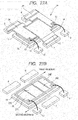
- Fig. 2A is a sectional perspective view of the part shown with the broken line in Fig. 1B in the semiconductor device 1 viewed from the direction shown with the solid-white arrow.
- Fig. 2B is a sectional perspective view showing the state (semiconductor chip 2) of removing the pectinate parts 3a, 3b, 4a, 4b, 4c, 5a, and 5b of the metal plate wires in the semiconductor device 1 shown in Fig. 2A .
- the heat sink 11 shown in Figs. 1A and 1B is omitted in Figs. 2A and 2B .
- a high side (control) switch T1 and a low side (synchronous) switch T2 are formed with power MISFETs (Metal Insulator Semiconductor Field Effect Transistors) respectively in the semiconductor chip 2.
- the power MISFET constituting the high side switch T1 has source electrodes 20, a drain electrode 22, and gate electrodes 24 over the top face side (identical face side) of the semiconductor chip.
- the power MISFET constituting the low side switch T2 has source electrodes 21, a drain electrode 23, and gate electrodes 25 over the top face side (identical face side) of the semiconductor chip.
- Such a power MISFET is also called a horizontal power MISFET.
- FIGS. 2A and 2B show the case where both the high side switch T1 and the low side switch T2 are n-channel type power MISFETs, the case where the high side switch T1 is a p-channel type power MISFET and the low side switch T2 is an n-channel type power MISFET is also acceptable.
- a MISFET may also be a MOS (Metal Oxide Semiconductor) type FET.
- MOS Metal Oxide Semiconductor
- the gate electrodes of a MISFET or a MOSFET any material can be used as long as the material is a conductor such as polysilicon and the material is not necessarily a metal.
- the high side (control) switch is also called a high side MISFET or a high side MIS type FET
- the low side (synchronous) switch is also called a low side MISFET or a low side MIS type FET.
- the high side switch T1 and the low side switch T2 formed in the semiconductor chip 2 are covered with the respective pectinate parts 3a, 3b, 4a, 4b, 4c, 5a, and 5b of the first, second, and third metal plate wires 3, 4, and 5.
- the pectinate parts 4d and 5c shown in Figs. 1A and 1B are not shown in the figures.
- the pectinate parts 3a, 3b, 4a, 4b, 4c, 5a, and 5b are coupled to the high side switch T1 and the low side switch T2 through source pads 26 and 27 and drain pads 28 and 29.
- Each of the first, second, and third metal plate wires 3, 4, and 5 having the pectinate parts 3a, 3b, 4a, 4b, 4c, 5a, and 5b preferably has a width (transverse direction in the section) of 0.3 mm or more for example and a thickness (vertical direction in the section) of 50 ⁇ m or more for example in the sections of Figs. 2A and 2B .
- the source pads 26 and the drain pad 28 are formed over the source electrodes 20, the drain electrode 22, and the gate electrodes 24.
- the source pad 27 and the drain pads 29 are formed over the source electrodes 21, the drain electrode 23, and the gate electrodes 25.
- a plurality of solder bumps 30 for being coupled to the pectinate parts 3a, 3b, 4a, and 4b are formed over the source pads 26 and the drain pad 28.
- a plurality of solder bumps 31 for being coupled to the pectinate parts 4b, 4c, 5a, and 5b are formed over the source pad 27 and the drain pads 29.
- the source pads 26 and 27 and the drain pads 28 and 29 in the semiconductor chip 2 are located under the first, second, and third metal plate wires 3, 4, and 5 so as to extend in the direction crossing the first, second, and third metal plate wires 3, 4, and 5.
- the source pads 26 and 27 and the drain pads 28 and 29 include aluminum (Al) for example but may also include copper (Cu).
- solder bumps 30 and 31 may be gold (Au) balls or copper (Cu) balls.
- Each of the source pads 26 and 27 and the drain pads 28 and 29 has a width (depth direction in the section) of 0.1 to 0.4 mm for example and a thickness (vertical direction in the section) of 1 to 10 ⁇ m for example in the section of Fig. 3 .
- source regions S1 and a drain region D1 of the high side switch T1 are formed in an N - -type well region 18a and source regions S2 and a drain region D2 of the low side switch T2 are formed in an N - -type well region 18b, respectively.
- the source regions S1 of the high side switch T1 are formed in P - -type well regions 19a formed in the N - -type well region 18a and the source regions S2 of the low side switch T2 are formed in P - -type well regions 19b formed in the N - -type well region 18b, respectively.
- each of the source electrodes 20 and 21 and the drain electrodes 22 and 23 has a width (transverse direction in the section) of 1 to 2 ⁇ m for example and a thickness (vertical direction in the section) of 0.1 to 1 ⁇ m for example in the sectional perspective views of Figs. 2A and 2B .
- the gate electrodes 24 are formed between the source regions S1 and the drain region D1 over the semiconductor substrate through gate insulation films GIa.
- the gate electrodes 25 are formed between the source regions S2 and the drain region D2 over the semiconductor substrate through gate insulation films GIb.
- Each of the gate electrodes 24 and 25 has a width of 0.5 to 2 ⁇ m for example and a thickness of 0.1 to 0.5 ⁇ m for example in the sections of Figs. 2A and 2B .
- Each of the gate insulation films GIa and GIb has a width of 0.5 to 2 ⁇ m for example and a thickness of 5 to 100 nm for example.
- the pectinate part 4b of the second metal plate wire 4 is coupled to the source pads 26 and the drain pads 29 through the solder bumps 30 and 31. That is, the source electrodes S1 of the high side switch T1 and the drain electrode D2 of the low side switch T2 formed in the semiconductor chip 2 are coupled to each other with the metal plate wire 4b of a single plate through the source pads 26, the drain pads 29, and the solder bumps 30 and 31.
- a region of the principal surface of the semiconductor chip 2 where the high side switch T1 is formed is defined as a first region R1 and a region of the principal surface of the semiconductor chip 2 where the low side switch T2 is formed is defined as a second region R2, respectively.
- Fig. 3 is a perspective view of the semiconductor chip 2 in the state of removing the metal plate wires, the input terminal, the output terminal, the ground terminal, the gate terminals, the heat sink, and the bonding wires of the semiconductor device 1 in Figs. 1A and 1B .
- the high side switch T1 is formed in the first region R1 of the principal surface of the semiconductor chip 2 and the low side switch T2 is formed in the second region R2 of the principal surface of the semiconductor chip 2. Then the source pads 26 and the drain pads 28 are allocated alternately over the first region R1 and the source pads 27 and the drain pads 29 are allocated alternately over the second region R2.
- first gate electrode pad 12 is formed in the vicinity of the upper right corner of the first region R1 and the second gate electrode pad 13 is formed in the vicinity of the lower right corner of the second region R2, respectively.
- the semiconductor chip 2 is a 2 in 1 chip wherein two switches (MISFETs) are formed in one semiconductor chip.
- Fig. 4A is a plan view of the surface of a semiconductor chip shown in Fig. 3 viewed from above and Fig. 4B is a sectional view taken on line A-A' in Fig. 4A .
- the high side switch T1 is formed in the first region of the semiconductor chip 2 having a quadrangular shape in a planar view and the low side switch T2 is formed in the second region of the semiconductor chip 2, respectively.
- the source pads 26 and the drain pads 28 are allocated alternately over the first region R1 and the source pads 27 and the drain pads 29 are allocated alternately over the second region R2.
- the source pads 26 and 27 and the drain pads 28 and 29 have strip-shapes or rectangular shapes in a planar view.
- the source pads 26 and 27 and the drain pads 28 and 29 are allocated so as to be located on identical lines. That is, one of the source pads 26 over the first region R1 and the relevant one of the drain pads 29 over the second region R2 are allocated so as to be located on an identical line over the principal surface of the semiconductor chip 2 in a planar view. Then one of the drain pads 28 over the first region R1 and the relevant one of the source pads 27 over the second region R2 are also allocated so as to be located on an identical line over the principal surface of the semiconductor chip 2 in a planar view.
- the first gate electrode pad 12 is formed in the vicinity of the upper right corner of the first region R1 and the second gate electrode pad 13 is formed in the vicinity of the lower right corner of the second region R2 respectively over the principal surface of the semiconductor chip 2.
- the plural solder bumps 31 are formed over the source pads 27 and the drain pads 29 allocated alternately.
- the plural solder bumps 30 are formed over the source pads 26 and the drain pads 28 allocated alternately.
- a first interlayer insulation film 49 formed under the source pads 26 and 27 and the drain pads 28 and 29 and a second interlayer insulation film 50 formed over the source pads 26 and 27 and the drain pads 28 and 29 are omitted.
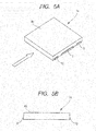
- Figs 5A and 5B are views showing an external appearance in the case of sealing the semiconductor device 1 with resin, in which Fig. 5A is a perspective view viewed obliquely from above and Fig. 5B is a side view viewed from the direction indicated with the solid-white arrow shown in Fig. 5A .
- Figs. 6A and 6B are views showing an external appearance of a semiconductor device 1a, in which Fig. 6A is a top view and Fig. 6B is a bottom view.
- Fig. 7 is a sectional view of the semiconductor device 1a taken on line A-A' in Fig. 6A .
- the first and second interlayer insulation films 49 and 50 are also omitted in the sectional view.
- the respective parts of the input terminal 6, the output terminal 7, the ground terminal 8, the first gate terminal 9, and the second gate terminal 10 are exposed over the side face of the encapsulation resin 46.
- the respective parts of the heat sink 11, the input terminal 6, the output terminal 7, the ground terminal 8, the first gate terminal 9, and the second gate terminal 10 are exposed over the bottom face of the encapsulation resin 46.
- the semiconductor chip 2 is coupled to the heat sink 11 through an adhesive 52 having a good heat dissipation and the parts of the second metal plate wire 4 and the third metal plate wire 5 located outside the semiconductor chip 2 are coupled to the output terminal 7 and the ground terminal 8 through the adhesive 52 having a good heat dissipation, respectively.
- the parts of the second metal plate wire 4 and the third metal plate wire 5 located over the semiconductor chip 2 are coupled to the semiconductor chip 2 through the solder bumps 31.
- each of the faces may have a chamfered external appearance.
- the right and left upper corners of the encapsulation resin 46 have chamfered shapes in the sectional view of Fig. 7 .
- FIG. 8 is an equivalent circuit schematic in the case of using the semiconductor device 1a for a DC/DC converter.
- the input terminal 6 of the semiconductor device 1 is coupled to an input voltage terminal VIN and also to an electrode of a condenser C1.
- the other electrode of the condenser C1 is coupled to a ground terminal GND.
- a choke coil L1 and an electrode of a condenser C2 are coupled to the output terminal 7 of the semiconductor device 1a and also to an output voltage terminal VOUT.
- the other electrode of the condenser C2 is coupled to the ground terminal GND.
- ground terminal 8 of the semiconductor device 1a is coupled to the ground terminal GND.
- first gate terminal 9 and the second gate terminal 10 of the semiconductor device 1a are coupled to a driver IC 32, respectively.
- the driver IC 32 is also coupled to the ground terminal GND.
- the driver IC 32 has: a driver to drive the high side switch and the low side switch; and a control circuit to control the driver.
- the semiconductor device 1a is configured by forming the high side switch and the low side switch of a non-insulated type DC/DC converter over a semiconductor chip 2.
- Fig. 9 is a schematic sectional view theoretically explaining the relation of connection among the high side switch T1, the low side switch T2, and the terminals such as the input terminal 6, the output terminal 7, and the ground terminal 8 in the semiconductor device 1 or 1a.
- the drain region D1 of the high side switch T1 is electrically coupled to the input terminal 6.
- the source regions S1 of the high side switch T1 are electrically coupled to the drain region D2 of the low side switch T2 and they are coupled to the output terminal 7. Further, the source regions S2 of the low side switch T2 are electrically coupled to the ground terminal 8.
- the gate electrode 24 of the high side switch T1 is electrically coupled to the first gate terminal 9 and the gate electrode 25 of the low side switch T2 is electrically coupled to the second gate terminal 10, respectively.
- Figs. 10A and 10B are views showing a mounting state in the case of forming a DC/DC converter by mounting the semiconductor device 1a over a wiring substrate 33 obtained by forming a multilayered wiring layer over a resinous insulating substrate, in which fig. 10A is a schematic plan view and Fig. 10B is a sectional view taken on line A-A' thereof.
- the semiconductor device 1a is mounted over a site shown with the broken line. Further, a driver IC 32, condensers C1 and C2, a choke coil L1, and a central processing unit CPU are mounted over the wiring substrate 33 excluding the site shown with the broken line.
- wires 35, 36, 37, 38, 39, 40, 41, and 42 are formed in the wiring substrate 33.
- the semiconductor device 1a is coupled to the condenser C1, the driver IC 32, the choke coil L1, and others through the wires 35, 36, 37, 38, 39, 40, 41, and 42.
- the DC/DC converter is structured so as to dissipate the heat generated in the semiconductor device 1a toward the bottom face side of the wiring substrate 33 through the wires 34 and thermal vias 34.
- wires (the wire 36, for example) on the top face side of the wiring substrate 33 are coupled to a wire 42r on the bottom face side or an upper layer wire 42u is coupled to a lower layer wire 42s.
- the input terminal 6 is coupled to the drain region D1 of the high side switch T1 through the first metal plate wire 3 having the pectinate parts 3a and 3b, the plural solder bumps 30, and the strip-shaped drain pads 28.
- the output terminal 7 is coupled to the source regions S1 of the high side switch T1 and the drain region D2 of the low side switch T2 through the second metal plate wire 4 having the pectinate parts 4a, 4b, 4c, and 4d, the plural solder bumps 30 and 31, and the strip-shaped source pads 26 and the drain pads 29.
- the ground terminal 8 is coupled to the source regions S2 of the low side switch T2 through the third metal plate wire 5 having the pectinate parts 5a, 5b, and 5c, the plural solder bumps 31, and the strip-shaped source pads 27.
- drain regions D1 and D2 and the source regions S1 and S2 of the high side switch T1 and the low side switch T2 are coupled to the input terminal 6, the output terminal 7, and the ground terminal 8 through the wide first, second, and third metal plate wires 3, 3a, 3b, 4, 4a, 4b, 4c, 4d, 5, 5a, 5b, and 5c, and the strip-shaped source pads 26 and 27 and drain pads 28 and 29, it is possible to improve heat dissipation and also reduce a parasitic resistance.
- metal plate wires are used for the connections in particular, it is possible to attain the improvement of heat dissipation and the reduction of a parasitic resistance far better than the case of connections with wires.
- thermal vias 34 are formed immediately under the semiconductor device 1a in the state of mounting the semiconductor device 1a over the thermal vias 34 formed in the wiring substrate 33 and hence the heat dissipation from the inner layer of the wiring substrate 33 through the bottom face improves further.
- the source pads 26 of the high side switch T1 and the drain pads 29 of the low side switch T2 are adjacently formed on identical lines over the principal surface of the semiconductor chip 2 in a planar view.
- the solder bumps 30 and the solder bumps 31 are formed on the sides where the source pads 26 and the drain pads 29 face each other.
- the source pads 26 of the high side switch T1 are electrically coupled to the drain pads 29 of the low side switch T2 through one (common) metal plate wire by coupling the pectinate part 4b of the second metal plate wire 4 over the solder bumps 30 and 31.
- the pectinate part 4b of the second metal plate wire 4 is coupled in the manner of straddling over the first region R1 of the high side switch T1 and the second region R2 of the low side switch T2. In this way, it is possible to reduce a wire inductance and obtain various effects including the improvement of an electric power source efficiency, the reduction of a surge voltage, the suppression of noises, etc.
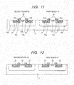
- a manufacturing method of a semiconductor device 1 is explained hereunder on the basis of Figs. 11 to 16 .
- N-type well regions 18a and 18b are formed in a selective first region R1 and a second region R2 that is different from the first region R1 over the principal surface of a semiconductor substrate 17 constituting a semiconductor wafer and P-type well regions 19a and 19b are formed in the N-type well regions 18a and 18b, respectively.
- gate electrodes 24 and 25 are formed over the principal surface where the N-type well regions 18a and 18b are formed through gate insulation films GIa and GIb.
- source regions S1 and S2 are formed in the P-type well regions 19a and 19b over the principal surface and moreover drain regions D1 and D2 are formed in regions distant from the source regions S1 and S2 and the P-type well regions 19a and 19b in the N-type well regions 18a and 18b.
- the N-type well region 18a, the P-type well regions 19a, the source regions S1, the drain region D1, and the gate electrodes 24 are formed in the first region R1.
- the N-type well region 18b, the P-type well regions 19b, the source regions S2, the drain region D2, and the gate electrodes 25 are formed in the second region R2.
- source electrodes 20 and 21 are formed over the source regions S1 and S2 and drain electrodes 22 and 23 are formed over the drain regions D1 and D2, respectively.
- a first interlayer insulation film 49 is formed over the gate electrodes 24 and 25, the source electrodes 20 and 21, and the drain electrodes 22 and 23 so as to cover them.
- a CVD film such as a CVD-SiO 2 film is used.
- a plasma CVD method, a thermal CDV method, or the like is used as a method for forming a CVD film.
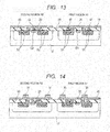
- tungsten plugs (connecting plugs) 47 and 48 are formed by selectively removing the first interlayer insulation film 49 over the source electrodes 20 and the drain electrode 23 and embedding a tungsten film in the removed parts.
- a source pad 26 and a drain pad 29 are formed by forming an aluminum (Al) film over the first interlayer insulation film 49 by a sputtering technology or the like and selectively removing the Al film.
- a source pad 27 and a drain pad 28 are not shown in Fig. 13 .
- the selective removal of the Al film is carried out by selective etching by a photolithography technology using a photoresist for example.
- a source pad 27, a drain pad 28, and tungsten plugs (connecting plugs) coupled to them not shown in Fig. 13 are formed also by the same method as described above.
- the source pad 26 is coupled to the source regions S1 of the high side switch T1 through the tungsten plugs 47 and the drain pad 29 is coupled to the drain region D2 of the low side switch T2 through the tungsten plug 48, respectively.
- a source pad 27 and a drain pad 28 not shown in Fig. 13 are also coupled to the high side switch T1 and the low side switch T2 through tungsten plugs in the same way as described above.
- a source pad 27 is coupled to source regions S2 of the low side switch T2 and a drain pad 28 is coupled to the drain region D1 of the high side switch T1, respectively.
- the source pads 26 and 27 and the drain pads 28 and 29 have strip-shapes or rectangular shapes in a planar view as is shown in Figs. 4A and 4B .
- solder bumps 30 and 31 are formed selectively over the source pad 26 and the drain pad 29.
- the solder bumps 30 and 31 are formed at sites of the adjacent source pad 26 and drain pad 29 closer to each other (positioned as shown in Fig. 2B ).
- solder bumps 30 and 31 are formed also over a source pad 27 and a drain pad 28 not shown in Fig. 14 in the same way as described above. On this occasion, the solder bumps 30 and 31 are formed at sites of the adjacent source pad 27 and drain pad 28 more distant from the ends facing each other (positioned as shown in Fig. 2B ).
- the solder bumps 30 and 31 are obtained by forming an Ni-Au plated film as an underlayer film in advance and forming them over the Ni-Au underlayer film.
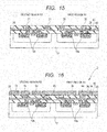
- a second interlayer insulation film 50 is formed over the source pad 26 and the drain pad 29 so as to embed the solder bumps 30 and 31 but expose the top faces of the solder bumps 30 and 31.
- the second interlayer insulation film 50 is formed also over a source pad 27 and a drain pad 28 not shown in Fig. 15 in the same way as described above. On this occasion, the second interlayer insulation film 50 is formed so as to expose the top faces of the solder bumps 30 and 31 over the source pad 27 and the drain pad 28 in the same way as described above.
- any one of a polyimide film, a CVD-SiO 2 film, and a CVD-SiN film or any one of the composite films thereof or a laminated film thereof is used.
- a semiconductor wafer after finishing the (e) process is divided into a plurality of semiconductor chips 2 each of which has a first region R1 and a second region R2. At this moment, a semiconductor chip 2 is prepared.
- first metal plate wires 3, 3a, and 3b, second metal plate wires 4, 4a, 4b, 4c, and 4d, and third metal plate wires 5, 5a, 5b, and 5c are: mounted over the top faces of the exposed solder bumps 30 and 31 and the second interlayer insulation film 50 of the semiconductor chip 2; and coupled to the solder bumps 30 and 31.
- metal plate wires 4d and 5c are not shown in Fig. 16 , the existence thereof is obvious from Figs. 1A and 1B and they are coupled to solder bumps in the same way as described above.
- Figs. 17A and 17B are sectional views supplementing the Fig. 16 process in Figs 17A and 17B .
- the cross sections in Figs 17A and 17B are the cross sections at the site identical to the cross section in Fig. 7 but are in the state of not yet being sealed with resin.
- solder bumps represented by the reference numeral 31 are shown.
- a heat sink 11, an output terminal 7, and a ground terminal 8 are shown but an input terminal 6, a first gate terminal 9, and a second gate terminal 10 are omitted in Fig. 7 because of a cross section of a specific site.
- the first interlayer insulation film 49 and the second interlayer insulation film 50 shown in Fig. 16 also omitted.
- the second metal plate wire 4 and the third metal plate wire 5 are located over the semiconductor chip 2 where the solder bumps 30 and 31 are formed. Only the solder bumps represented by the reference numeral 31 are shown because of the sectional view. As is shown in Fig. 17B , the second metal plate wire 4 and the third metal plate wire 5, the solder bumps 30 and 31, and the output terminal 7 and the ground terminal 8 are coupled to each other. Further, the semiconductor chip 2 is coupled to the heat sink 11. Only the solder bumps represented by the reference numeral 31 are shown because of the sectional view. An adhesive 52 having a good heat dissipation is used for the coupling between the semiconductor chip 2 and the heat sink 11, the coupling between the second metal plate wire 4 and the output terminal 7, and the coupling between the third metal plate wire 5 and the ground terminal 8, respectively.
- the semiconductor device 1 is sealed with an encapsulation resin 46 by a transfer mold method for example and thus a semiconductor device 1a is formed.
- Fig. 18 is a perspective view showing a semiconductor device according to Embodiment 2.
- Embodiment 2 is a case of forming the input terminal 6, the output terminal 7, and the ground terminal 8 in the semiconductor device 1 shown in Fig. 1 as Embodiment 1 with parts of the first, second, and third metal plate wires, respectively. That is, this is a case of forming an input terminal 6 with a part of a first metal plate wire 3A, an output terminal 7 with a part of a second metal plate wire 4A, and a ground terminal 8 with a part of a third metal plate wire 5A, respectively. Others than those are the same as Embodiment 1.
- Embodiment 2 since it is unnecessary to use an input terminal 6, an output terminal 7, and a ground terminal 8 respectively, it is possible not only to obtain effects similar to Embodiment 1 but also to reduce the number of the manufacturing processes and the manufacturing cost of a semiconductor device 1A.
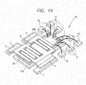
- Fig. 19 is a perspective view showing a semiconductor device according to Embodiment 3.
- Embodiment 3 in addition to the high side switch T1 and the low side switch T2 shown in Embodiment 1, a drive control circuit 32B having the function of the driver IC 32 is formed over the principal surface of a semiconductor chip 2B.
- a drive control circuit 32B, a high side switch T1 and a low side switch T2 are formed in the longitudinal direction over the principal surface of a rectangular semiconductor chip 2B.
- a plurality of bonding pads 56 are coupled to a plurality of terminals 53 through a plurality of bonding wires (third bonding wires) 51 in the drive control circuit 32B.
- Figs. 20A and 20B are views showing the state of sealing the semiconductor device 1B shown in Fig. 19 with resin, in which Fig. 20A is a perspective view thereof and Fig. 20B is a side view viewed from the direction of the arrow.
- Fig. 21A is a top view and Fig. 21B is a bottom view of the semiconductor device 1Ba shown in Figs. 20A and 20B .
- a semiconductor device 1Ba is obtained by sealing the semiconductor device 1B with resin by a transfer mold technology for example.
- each of the top face, the bottom face, and the side faces of the encapsulation resin 46 of the semiconductor device 1Ba has a quadrangular shape, each of them may have an external appearance having chamfered corners.
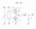
- Fig. 22 is an equivalent circuit schematic in the case of using a semiconductor device 1Ba for a DC/DC converter.
- An input terminal 6 in the semiconductor device 1Ba is coupled to an input voltage terminal VIN and also to an electrode of a condenser C1 and the other electrode of the condenser C1 is coupled to a ground terminal GND. Then a choke coil L1 and an electrode of a condenser C2 are coupled to an output terminal 7 in the semiconductor device 1Ba and also coupled to an output voltage terminal VOUT. The other electrode of the condenser C2 is coupled to the ground terminal GND.
- a ground terminal 8 in the semiconductor device 1Ba is coupled to the ground terminal GND.
- a gate electrode 24 of a high side switch T1 and a gate electrode 25 of a low side switch T2 in the semiconductor device 1Ba are coupled to a drive control circuit 32B respectively in a semiconductor chip 2B. That is, the gate electrode 24 of the high side switch T1 and the gate electrode 25 of the low side switch T2 are coupled to the drive control circuit 32B respectively through wires including a diffusion layer formed in the semiconductor chip 2B or wires including a metal layer, wires including a polycrystalline silicon layer, or wires including the combination thereof, those being formed over the semiconductor chip 2B. Further, the drive control circuit 32B is also coupled to the ground potential GND.
- Embodiment 3 since a high side switch T1, a low side switch T2, and a drive control circuit 32B are formed in a semiconductor chip 2B and they are coupled in the semiconductor chip 2B, it is possible to reduce wiring resistance between elements and further reduce noises. Further, it is possible to further reduce a wiring inductance. Furthermore, in Embodiment 3, effects similar to Embodiment 1 can be obtained.
- Fig. 23 is a perspective view showing a semiconductor device according to Embodiment 4.
- a semiconductor device 1Ca As is obvious from the figure, respective parts of a first metal plate wire 3, a second metal plate wire 4, and a third metal plate wire 5 are exposed from the surface of an encapsulation resin 46 of a semiconductor device 1a. Others than that are identical to Embodiments 1 and 2.
- Embodiment 4 it is possible not only to obtain effects similar to Embodiment 1 but also to improve heat dissipation from the surface side of an encapsulation resin 46. Further, it is possible to further improve the heat dissipation by coupling radiation fins or the like to the exposed parts.
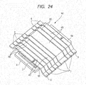
- Fig. 24 is a perspective view showing a semiconductor device according to Embodiment 5.
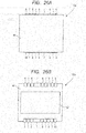
- Figs. 25A and 25B are views showing the state of sealing the semiconductor device 1D shown in Fig. 24 with an encapsulation resin 46, in which Fig. 25A is a perspective view thereof and Fig. 25B is a side view viewed from the direction indicated with the solid-white arrow.
- Fig. 26A is a top view and Fig. 26B is a bottom view of the semiconductor device 1Da shown in Figs. 25A and 25B .
- Embodiment 5 is based on a semiconductor chip 2 according to Embodiment 1, namely a semiconductor chip 2 in the state of having source pads 26 and 27, drain pads 28 and 29, solder bumps 30 and 31, a first gate electrode pad 12, and a second gate electrode pad 13.
- the semiconductor chip 2 is prepared and a plurality of long and thin first metal plate wires 3D, a plurality of second metal plate wires 4D, and a plurality of third metal plate wires 5D are allocated respectively over the semiconductor chip 2 as shown in Fig. 24 and coupled to solder bumps 30 and 31 respectively.
- the plural first metal plate wires 3D and the plural second metal plate wires 4D are allocated alternately and the plural second metal plate wires 4D and the plural third metal plate wires 5D are also allocated alternately over the top plane of the semiconductor chip 2.
- a fourth metal plate wire 54 is coupled to the first gate electrode pad 12 and a fifth metal plate wire 55 is coupled to the second gate electrode pad 13, respectively.
- the first metal plate wires 3D have input terminals 6 at sites distant from above the semiconductor chip 2.
- the second metal plate wires 4D have output terminals 7 at sites distant from above the semiconductor chip 2.
- the third metal plate wires 5D have ground terminals 8 at sites distant from above the semiconductor chip 2.
- Each of the first metal plate wires 3D, the second metal plate wires 4D, the third metal plate wires 5D, the fourth metal plate wire 54, and the fifth metal plate wire 55 includes a horizontally long plate.
- source pads 26 of a high side switch T1 and drain pads 29 of a low side switch T2 are coupled through the second metal plate wires 4D including a metal plate. That is, the second metal plate wires 4D are commonly used for the coupling.
- a semiconductor device 1Da is formed by sealing the semiconductor device 1D with resin by a transfer mold technology for example.
- the semiconductor device 1Da sealed with an encapsulation resin 46 respective parts of an input terminal 6, an output terminal 7, a ground terminal 8, a first gate terminal 9, and a second gate terminal 10 are exposed on a side face of the encapsulation resin 46.
- respective parts of a heat sink 11, the input terminal 6, the output terminal 7, the ground terminal 8, the first gate terminal 9, and the second gate terminal 10 are exposed on the bottom face of the encapsulation resin 46 as is shown in Fig. 26B .
- the external appearance of each of the top face, the bottom face, and the side faces of the encapsulation resin 46 of the semiconductor device 1Da has a quadrangular shape, each of them may have an external appearance having chamfered corners.
- Embodiment 5 it is possible to attain the reduction of a wire inductance, the improvement of heat dissipation, the reduction of a parasitic resistance, etc. in the same way as Embodiments 1 to 4.
- first, second, and third metal plate wires 3D, 4D, and 5D have simple shapes, the manufacturing and processing are facilitated and the manufacturing cost of a semiconductor device is reduced.
- Figs. 27A and 27B are perspective views showing a semiconductor device according to Embodiment 6.
- Fig. 27A represents the state of not being sealed with an encapsulation resin and
- Fig. 27B represents the state of removing a first metal plate wire, a second metal plate wire, and a third metal plate wire from the state in Fig. 27A .
- strip-shaped source pads 26 and 27 and drain pads 28 and 29 are not allocated over a high side switch T1 and a low side switch T2 respectively unlike Embodiments 1 to 5 and planar source pads 26E and 27E and planar drain pads 28E and 29E are allocated over a first region R1 where a high side switch T1 exists and a second region R2 where a low side switch T2 exists as shown in Fig. 27B .
- the source pad 26E and the drain pad 28E are allocated over the first region R1 and the source pad 27E and the drain pad 29E are allocated over the second region R2, respectively.
- a first gate electrode pad 12 is formed in the vicinity of the upper right corner of the first region R1 and a second gate electrode pad 13 is formed in the vicinity of the lower right corner of the second region R2, respectively.
- a first metal plate wire 3E is electrically coupled over the drain pad 28E and a third metal plate wire 5E is electrically coupled over the source pad 27E, respectively.
- a second metal plate wire 4E is electrically coupled over the source pad 26E and the drain pad 29E as a common metal plate.
- a part of the first metal plate wire 3E extending outward from above a semiconductor chip 2E is electrically coupled to an input terminal 6.
- a part of the second metal plate wire 4E extending outward from above the semiconductor chip 2E is also electrically coupled to an output terminal 7.
- a part of the third metal plate wire 5E extending outward from above the semiconductor chip 2E is also electrically coupled to a ground terminal 8.
- the input terminal 6, the output terminal 7, and the ground terminal 8 are located outside the semiconductor chip 2E.
- first gate electrode pad 12 is coupled to a first gate terminal 9 located outside the semiconductor chip 2E through a bonding wire 14.
- the second gate electrode pad 13 is also coupled to a second gate terminal 10 located outside the semiconductor chip 2E through a bonding wire 15.
- the semiconductor chip 2E is identical to the semiconductor chip 2 except that the shapes of the source pads 26E and 27E and the drain pads 28E and 29E are different.
- Embodiment 6 it is possible to obtain various effects such as the improvement of heat dissipation, the reduction of a parasitic resistance, the reduction of a wire inductance, the improvement of an electric power source efficiency, the reduction of a surge voltage, the inhibition of noises, etc. in the same way as Embodiment 1.
- a semiconductor device may not be sealed with a resin but be sealed with another insulative material such as ceramics.
- source pads 26 and 27 and drain pads 28 and 29 include copper (Cu)
- solder bumps formed selectively over the pads may be formed through an Ni-Au plated film selectively formed over copper (Cu); or may be formed over copper (Cu) pads in a non-plated state of not forming an Ni-Au plated film.
- an insulation film may be applied or formed over the surface of a wire in order to prevent the wire from being oxidized.
Landscapes
- Engineering & Computer Science (AREA)
- Power Engineering (AREA)
- Semiconductor Integrated Circuits (AREA)
- Internal Circuitry In Semiconductor Integrated Circuit Devices (AREA)
- Cooling Or The Like Of Semiconductors Or Solid State Devices (AREA)
- Dc-Dc Converters (AREA)
- Structures Or Materials For Encapsulating Or Coating Semiconductor Devices Or Solid State Devices (AREA)
- Metal-Oxide And Bipolar Metal-Oxide Semiconductor Integrated Circuits (AREA)
- Junction Field-Effect Transistors (AREA)
- Wire Bonding (AREA)
Abstract
Description
- The disclosure of Japanese Patent Application No.
2012-030383 filed on February 15, 2012 - The present invention relates to a semiconductor device, for example to a technology effectively applicable to a semiconductor device used for a power supply circuit.
- A DC/DC converter widely used as a power supply circuit includes a high side switch, a low side switch, drivers (drive circuits) to drive the switches, a control circuit to control the drivers, etc. In each of the high side switch and the low side switch, a power MOSFET (Metal Oxide Semiconductor Field Effect Transistor) is used. Here, a high side switch is also called a control switch and a low side switch is also called a synchronous switch.
- In a semiconductor device used for a power supply circuit such as a DC/DC converter, for example the following technologies are proposed with the aim of downsizing and reducing the inductance of a wire.
- A power MOSFET for a high side switch, a drive circuit to drive the power MOSFET for the high side switch, and a drive circuit to drive a power MOSFET for a low side switch are formed in one semiconductor chip. A power MOSFET for the low side switch is formed in another chip. The two semiconductor chips are contained in one package.
- A power MOSFET for a high side switch, a power MOSFET for a low side switch, and drivers and control circuits for them are formed over one semiconductor substrate.
-
- [Patent Literature 1]
Japanese Unexamined Patent Publication No.2005-203584 - [Patent Literature 2]
Japanese Unexamined Patent Publication No.2010-16035 -
Patent Literature 1 describes the evaluations on the parameters of wire inductance, on resistance, downsizing, and heat dissipation inFig. 13 of the patent publication with regard to the examples of the systems inFigs. 8 to 12 of the patent publication. As is obvious fromFig. 13 , the three cases inFigs. 8 ,10 , and12 ofPatent Literature 1 have the problem of heat dissipation. Meanwhile, the case inFig. 9 shows a moderate heat dissipation but has the problems of downsizing and the like. The case inFig. 11 has the problem of downsizing. - Successively,
Patent Literature 2 only describes how a power MOSFET for a high side switch, a power MOSFET for a low side switch, drivers for them, and others are allocated over one semiconductor substrate but does not take the problems of heat dissipation and others into consideration. - Other problems and novel features will be obvious from the descriptions and attached drawings in the present specification.
- A semiconductor device according to an embodiment has a structure formed by covering a principal surface of a semiconductor chip having the principal surface and a plurality of MIS-type FETs formed over the principal surface with a plurality of metal plate wires having pectinate shapes and being allocated alternately in a planar view.
- In the embodiment, it is possible to obtain a semiconductor device capable of downsizing and on top of that capable of improving heat dissipation.
-
-
Figs. 1A and 1B are perspective views showing a semiconductor device according toEmbodiment 1. -
Figs. 2A and 2B are sectional perspective views of a semiconductor device according toEmbodiment 1. -
Fig. 3 is a perspective view of a semiconductor chip according toEmbodiment 1. -
Fig. 4A is a plan view of the surface of a semiconductor chip shown inFig. 3 viewed from above andFig. 4B is a sectional view thereof. -
Figs 5A and 5B are views showing an external appearance in the case of sealing a semiconductor device shown inFig. 1 with resin. -
Figs. 6A and 6B are views showing an external appearance of a semiconductor device shown inFigs. 5A and 5B , in whichFig. 6A is a top view andFig. 6B is a bottom view. -
Fig. 7 is a sectional view of a semiconductor device taken on line A-A' ofFig. 6A . -
Fig. 8 is an equivalent circuit schematic in the case of using a semiconductor device shown inFigs. 1A to 7 for a DC/DC converter. -
Fig. 9 is a schematic sectional view theoretically explaining the relation of connection of terminals in a semiconductor chip according toEmbodiment 1. -
Figs. 10A and 10B are views showing a mounting state in the case of forming a DC/DC converter by mounting a semiconductor device shown inFigs. 1A to 7 on a wiring substrate. -
Fig. 11 is a sectional view in (a) process showing a manufacturing method of a semiconductor device according toEmbodiment 1. -
Fig. 12 is a sectional view in (b) process showing a manufacturing method of a semiconductor device according toEmbodiment 1. -
Fig. 13 is a sectional view in (c) process showing a manufacturing method of a semiconductor device according toEmbodiment 1. -
Fig. 14 is a sectional view in (d) process showing a manufacturing method of a semiconductor device according toEmbodiment 1. -
Fig. 15 is a sectional view in (e) process showing a manufacturing method of a semiconductor device according toEmbodiment 1. -
Fig. 16 is a sectional view in (g) process showing a manufacturing method of a semiconductor device according toEmbodiment 1. -
Figs. 17A and 17B are sectional views supplementing the (g) process in the manufacturing method. -
Fig. 18 is a perspective view showing a semiconductor device according toEmbodiment 2. -
Fig. 19 is a perspective view showing a semiconductor device according toEmbodiment 3. -
Figs. 20A and 20B are views showing an external appearance in the case of sealing a semiconductor device inFig. 19 with resin. -
Fig. 21A is a top view andFig. 21B is a bottom view of a semiconductor device shown inFigs. 20A and 20B . -
Fig. 22 is an equivalent circuit schematic in the case of using a semiconductor device shown inFigs. 19 to 21B for a DC/DC converter. -
Fig. 23 is a perspective view showing a resin-sealed type semiconductor device according toEmbodiment 4. -
Fig. 24 is a perspective view showing a semiconductor device according toEmbodiment 5. -
Figs. 25A and 25B are views showing an external appearance in the case of sealing a semiconductor device inFig. 24 with resin. -
Fig. 26A is a top view andFig. 26B is a bottom view of a semiconductor device shown inFigs. 25A and 25B . -
Figs. 27A and 27B are perspective views showing a semiconductor device according toEmbodiment 6. - Embodiments are explained hereunder in detail in reference to drawings.
- In the following embodiments, explanations are made in the manner of being divided into plural sections or embodiments for convenience when it is necessary. Unless otherwise specified however, they are not unrelated to each other and one is related to another as a modified example, an application, a detailed explanation, or a supplemental remark of a part or the whole thereof. Further, in the following embodiments, when the number of components or the like (including the number of pieces, a numerical value, a quantity, a range, etc.) is mentioned, the number is not particularly limited to the specific number and may be more or less than the specific number. Here, the case of being otherwise specified or obviously limited to the specific number in principle is excluded.
- Furthermore, in the following embodiments, constituent components (including component steps) are not always essential unless otherwise specified or considered to be essential in principle. Similarly, in the following embodiments, when a shape, positional relationship, etc. of a constituent component or the like are mentioned, a shape or the like which is substantially close or similar to the shape is included. Here, the case of being otherwise specified or considered to be otherwise in principle is excluded. The same goes for a number or the like (including the number of pieces, a numerical value, a quantity, a range, etc.) stated above.
- Here, in all the drawings for explaining the embodiments, members having an identical function are represented with an identical or related code and repetitive explanations are omitted. In the following embodiments, explanations on identical or similar components are not repeated in principle except when particularly necessary.
-
Fig. 1A is a perspective view showing a semiconductor device according toEmbodiment 1 andFig. 1B is a perspective view of a semiconductor device showing the part described inFigs. 2A and 2B that will be explained later with the broken line. Here,Figs. 1A and 1B are the views showing a semiconductor device in the state of removing an encapsulation resin. - As is shown in
Figs. 1A and 1B , asemiconductor device 1 includes asemiconductor chip 2, a firstmetal plate wire 3, a secondmetal plate wire 4, a thirdmetal plate wire 5, aninput terminal 6, anoutput terminal 7, aground terminal 8, afirst gate terminal 9, asecond gate terminal 10, aheat sink 11, andbonding wires semiconductor chip 2 has a first gate electrode pad (high side gate electrode pad) 12 and a second gate electrode pad (low side gate electrode pad) 13. - The pectinate first
metal plate wire 3, the pectinate secondmetal plate wire 4, and the pectinate thirdmetal plate wire 5 are formed so as to extend from the outside of thesemiconductor chip 2 over a principal surface of thesemiconductor chip 2, respectively. The firstmetal plate wire 3 haspectinate parts metal plate wire 4 haspectinate parts metal plate wire 5 haspectinate parts - The respective pectinate parts of the first
metal plate wire 3, the secondmetal plate wire 4, and the thirdmetal plate wire 5 are alternately allocated in a planar view so as to cover the principal surface of thesemiconductor chip 2. Further, the part of the firstmetal plate wire 3 located outside thesemiconductor chip 2 is electrically coupled to theinput terminal 6. The part of the secondmetal plate wire 4 located outside thesemiconductor chip 2 is electrically coupled to theoutput terminal 7. The part of the thirdmetal plate wire 5 located outside thesemiconductor chip 2 is electrically coupled to theground terminal 8. Theinput terminal 6, theoutput terminal 7, and theground terminal 8 are allocated outside thesemiconductor chip 2, respectively. - Further, the first
gate electrode pad 12 is coupled to the first gate terminal (high side gate terminal) 9 located outside thesemiconductor chip 2 through thebonding wire 14. The secondgate electrode pad 13 is also coupled to the second gate terminal (low side gate terminal) 10 located outside thesemiconductor chip 2 through thebonding wire 15. - Furthermore, a frame including a solid plate used as the
heat sink 11 is coupled to the other principal surface (rear surface of the semiconductor chip 2) on the other side of the principal surface of thesemiconductor chip 2. - The first
metal plate wire 3, the secondmetal plate wire 4, the thirdmetal plate wire 5, theheat sink 11, theinput terminal 6, theoutput terminal 7, and theground terminal 8 are formed by pressing or etching a copper (Cu) plate for example. - As the
bonding wires - The
semiconductor chip 2 has a rectangular shape in a planar view but may also have a square shape. That is, any shape is acceptable as long as the shape has four sides in a planar view. -
Fig. 2A is a sectional perspective view of the part shown with the broken line inFig. 1B in thesemiconductor device 1 viewed from the direction shown with the solid-white arrow.Fig. 2B is a sectional perspective view showing the state (semiconductor chip 2) of removing thepectinate parts semiconductor device 1 shown inFig. 2A . Here, theheat sink 11 shown inFigs. 1A and 1B is omitted inFigs. 2A and 2B . - As is shown in
Fig. 2B , a high side (control) switch T1 and a low side (synchronous) switch T2 are formed with power MISFETs (Metal Insulator Semiconductor Field Effect Transistors) respectively in thesemiconductor chip 2. The power MISFET constituting the high side switch T1 hassource electrodes 20, adrain electrode 22, andgate electrodes 24 over the top face side (identical face side) of the semiconductor chip. The power MISFET constituting the low side switch T2 hassource electrodes 21, adrain electrode 23, andgate electrodes 25 over the top face side (identical face side) of the semiconductor chip. Such a power MISFET is also called a horizontal power MISFET. AlthoughFigs. 2A and 2B show the case where both the high side switch T1 and the low side switch T2 are n-channel type power MISFETs, the case where the high side switch T1 is a p-channel type power MISFET and the low side switch T2 is an n-channel type power MISFET is also acceptable. - A MISFET may also be a MOS (Metal Oxide Semiconductor) type FET. As the gate electrodes of a MISFET or a MOSFET, any material can be used as long as the material is a conductor such as polysilicon and the material is not necessarily a metal.
- The high side (control) switch is also called a high side MISFET or a high side MIS type FET, and the low side (synchronous) switch is also called a low side MISFET or a low side MIS type FET.
- As is obvious from
Figs. 2A and 2B , the high side switch T1 and the low side switch T2 formed in thesemiconductor chip 2 are covered with the respectivepectinate parts metal plate wires pectinate parts Figs. 1A and 1B are not shown in the figures. - The
pectinate parts source pads drain pads - Each of the first, second, and third
metal plate wires pectinate parts Figs. 2A and 2B . - As is obvious from
Figs. 2A and 2B , thesource pads 26 and thedrain pad 28 are formed over thesource electrodes 20, thedrain electrode 22, and thegate electrodes 24. Thesource pad 27 and thedrain pads 29 are formed over thesource electrodes 21, thedrain electrode 23, and thegate electrodes 25. Then a plurality of solder bumps 30 for being coupled to thepectinate parts source pads 26 and thedrain pad 28. Further, a plurality of solder bumps 31 for being coupled to thepectinate parts source pad 27 and thedrain pads 29. - The
source pads drain pads semiconductor chip 2 are located under the first, second, and thirdmetal plate wires metal plate wires source pads drain pads - Further, the solder bumps 30 and 31 may be gold (Au) balls or copper (Cu) balls.
- Each of the
source pads drain pads Fig. 3 . - Further, source regions S1 and a drain region D1 of the high side switch T1 are formed in an N--
type well region 18a and source regions S2 and a drain region D2 of the low side switch T2 are formed in an N--type well region 18b, respectively. - Then the source regions S1 of the high side switch T1 are formed in P--
type well regions 19a formed in the N--type well region 18a and the source regions S2 of the low side switch T2 are formed in P--type well regions 19b formed in the N--type well region 18b, respectively. - Then the
source electrodes 20 are formed over the source regions S1 and thesource electrodes 21 are formed over the source regions S2, respectively. Further, thedrain electrode 22 is formed over the drain region D1 and thedrain electrode 23 is formed over the drain region D2, respectively. Each of thesource electrodes drain electrodes Figs. 2A and 2B . - Further, the
gate electrodes 24 are formed between the source regions S1 and the drain region D1 over the semiconductor substrate through gate insulation films GIa. Likewise, thegate electrodes 25 are formed between the source regions S2 and the drain region D2 over the semiconductor substrate through gate insulation films GIb. Each of thegate electrodes Figs. 2A and 2B . Each of the gate insulation films GIa and GIb has a width of 0.5 to 2 µm for example and a thickness of 5 to 100 nm for example. - As is obvious from
Figs. 2A and 2B , thepectinate part 4b of the secondmetal plate wire 4 is coupled to thesource pads 26 and thedrain pads 29 through the solder bumps 30 and 31. That is, the source electrodes S1 of the high side switch T1 and the drain electrode D2 of the low side switch T2 formed in thesemiconductor chip 2 are coupled to each other with themetal plate wire 4b of a single plate through thesource pads 26, thedrain pads 29, and the solder bumps 30 and 31. - A region of the principal surface of the
semiconductor chip 2 where the high side switch T1 is formed is defined as a first region R1 and a region of the principal surface of thesemiconductor chip 2 where the low side switch T2 is formed is defined as a second region R2, respectively. -
Fig. 3 is a perspective view of thesemiconductor chip 2 in the state of removing the metal plate wires, the input terminal, the output terminal, the ground terminal, the gate terminals, the heat sink, and the bonding wires of thesemiconductor device 1 inFigs. 1A and 1B . - As is shown in
Fig. 3 , the high side switch T1 is formed in the first region R1 of the principal surface of thesemiconductor chip 2 and the low side switch T2 is formed in the second region R2 of the principal surface of thesemiconductor chip 2. Then thesource pads 26 and thedrain pads 28 are allocated alternately over the first region R1 and thesource pads 27 and thedrain pads 29 are allocated alternately over the second region R2. - Further, the first
gate electrode pad 12 is formed in the vicinity of the upper right corner of the first region R1 and the secondgate electrode pad 13 is formed in the vicinity of the lower right corner of the second region R2, respectively. - The
semiconductor chip 2 is a 2 in 1 chip wherein two switches (MISFETs) are formed in one semiconductor chip. -
Fig. 4A is a plan view of the surface of a semiconductor chip shown inFig. 3 viewed from above andFig. 4B is a sectional view taken on line A-A' inFig. 4A . - As is obvious from
Figs. 4A and 4B , the high side switch T1 is formed in the first region of thesemiconductor chip 2 having a quadrangular shape in a planar view and the low side switch T2 is formed in the second region of thesemiconductor chip 2, respectively. As is shown inFig. 3 , thesource pads 26 and thedrain pads 28 are allocated alternately over the first region R1 and thesource pads 27 and thedrain pads 29 are allocated alternately over the second region R2. - Further, as is shown in
Figs. 4A and 4B , thesource pads drain pads - Further, the
source pads drain pads source pads 26 over the first region R1 and the relevant one of thedrain pads 29 over the second region R2 are allocated so as to be located on an identical line over the principal surface of thesemiconductor chip 2 in a planar view. Then one of thedrain pads 28 over the first region R1 and the relevant one of thesource pads 27 over the second region R2 are also allocated so as to be located on an identical line over the principal surface of thesemiconductor chip 2 in a planar view. - As is shown in
Fig. 3 , the firstgate electrode pad 12 is formed in the vicinity of the upper right corner of the first region R1 and the secondgate electrode pad 13 is formed in the vicinity of the lower right corner of the second region R2 respectively over the principal surface of thesemiconductor chip 2. - Successively, as is shown in
Fig. 4B , in the second region R2, the plural solder bumps 31 are formed over thesource pads 27 and thedrain pads 29 allocated alternately. Likewise, in the first region R1, the plural solder bumps 30 are formed over thesource pads 26 and thedrain pads 28 allocated alternately. - In the
semiconductor device 1 and thesemiconductor chip 2 described inFigs. 1A to 4B , a firstinterlayer insulation film 49 formed under thesource pads drain pads interlayer insulation film 50 formed over thesource pads drain pads -
Figs 5A and 5B are views showing an external appearance in the case of sealing thesemiconductor device 1 with resin, in whichFig. 5A is a perspective view viewed obliquely from above andFig. 5B is a side view viewed from the direction indicated with the solid-white arrow shown inFig. 5A .Figs. 6A and 6B are views showing an external appearance of asemiconductor device 1a, in whichFig. 6A is a top view andFig. 6B is a bottom view.Fig. 7 is a sectional view of thesemiconductor device 1a taken on line A-A' inFig. 6A . The first and secondinterlayer insulation films - As is shown in
Figs. 5A to 7 , in thesemiconductor device 1a formed by sealing thesemiconductor device 1 with anencapsulation resin 46, the respective parts of theinput terminal 6, theoutput terminal 7, theground terminal 8, thefirst gate terminal 9, and thesecond gate terminal 10 are exposed over the side face of theencapsulation resin 46. - Further, as is shown in
Fig. 6B , the respective parts of theheat sink 11, theinput terminal 6, theoutput terminal 7, theground terminal 8, thefirst gate terminal 9, and thesecond gate terminal 10 are exposed over the bottom face of theencapsulation resin 46. - Furthermore, as is obvious from the sectional view of
Fig. 7 , thesemiconductor chip 2 is coupled to theheat sink 11 through an adhesive 52 having a good heat dissipation and the parts of the secondmetal plate wire 4 and the thirdmetal plate wire 5 located outside thesemiconductor chip 2 are coupled to theoutput terminal 7 and theground terminal 8 through the adhesive 52 having a good heat dissipation, respectively. The parts of the secondmetal plate wire 4 and the thirdmetal plate wire 5 located over thesemiconductor chip 2 are coupled to thesemiconductor chip 2 through the solder bumps 31. - Although the external appearances of the top face, the bottom face, and the side faces of the
encapsulation resin 46 in thesemiconductor device 1a are quadrangles, each of the faces may have a chamfered external appearance. In this case therefore, the right and left upper corners of theencapsulation resin 46 have chamfered shapes in the sectional view ofFig. 7 . - Successively,
Fig. 8 is an equivalent circuit schematic in the case of using thesemiconductor device 1a for a DC/DC converter. - As is obvious from
Fig. 8 , theinput terminal 6 of thesemiconductor device 1 is coupled to an input voltage terminal VIN and also to an electrode of a condenser C1. The other electrode of the condenser C1 is coupled to a ground terminal GND. Then a choke coil L1 and an electrode of a condenser C2 are coupled to theoutput terminal 7 of thesemiconductor device 1a and also to an output voltage terminal VOUT. The other electrode of the condenser C2 is coupled to the ground terminal GND. - Further, the
ground terminal 8 of thesemiconductor device 1a is coupled to the ground terminal GND. Furthermore, thefirst gate terminal 9 and thesecond gate terminal 10 of thesemiconductor device 1a are coupled to adriver IC 32, respectively. Thedriver IC 32 is also coupled to the ground terminal GND. Thedriver IC 32 has: a driver to drive the high side switch and the low side switch; and a control circuit to control the driver. - As is stated above, the
semiconductor device 1a is configured by forming the high side switch and the low side switch of a non-insulated type DC/DC converter over asemiconductor chip 2. -
Fig. 9 is a schematic sectional view theoretically explaining the relation of connection among the high side switch T1, the low side switch T2, and the terminals such as theinput terminal 6, theoutput terminal 7, and theground terminal 8 in thesemiconductor device - In the figure, a representative structure is shown as the structure of the high side switch T1 and the low side switch T2 because of the schematic sectional view.
- As is obvious from the figure, the drain region D1 of the high side switch T1 is electrically coupled to the
input terminal 6. The source regions S1 of the high side switch T1 are electrically coupled to the drain region D2 of the low side switch T2 and they are coupled to theoutput terminal 7. Further, the source regions S2 of the low side switch T2 are electrically coupled to theground terminal 8. Thegate electrode 24 of the high side switch T1 is electrically coupled to thefirst gate terminal 9 and thegate electrode 25 of the low side switch T2 is electrically coupled to thesecond gate terminal 10, respectively. -
Figs. 10A and 10B are views showing a mounting state in the case of forming a DC/DC converter by mounting thesemiconductor device 1a over awiring substrate 33 obtained by forming a multilayered wiring layer over a resinous insulating substrate, in whichfig. 10A is a schematic plan view andFig. 10B is a sectional view taken on line A-A' thereof. - As is shown in the figures, the
semiconductor device 1a is mounted over a site shown with the broken line. Further, adriver IC 32, condensers C1 and C2, a choke coil L1, and a central processing unit CPU are mounted over thewiring substrate 33 excluding the site shown with the broken line. - Furthermore,
wires wiring substrate 33. - Then the
semiconductor device 1a is coupled to the condenser C1, thedriver IC 32, the choke coil L1, and others through thewires - Further, as is obvious from
Fig. 10B , the DC/DC converter is structured so as to dissipate the heat generated in thesemiconductor device 1a toward the bottom face side of thewiring substrate 33 through thewires 34 andthermal vias 34. - Furthermore, through through
holes 43, wires (thewire 36, for example) on the top face side of thewiring substrate 33 are coupled to awire 42r on the bottom face side or anupper layer wire 42u is coupled to alower layer wire 42s. - In the mounting over the
wiring substrate 33, it is also possible to mount thesemiconductor device 1 before sealed with resin, pot a resin for protection after the mounting, and thus protect thesemiconductor device 1 with the potting resin. - In the
semiconductor device input terminal 6 is coupled to the drain region D1 of the high side switch T1 through the firstmetal plate wire 3 having thepectinate parts drain pads 28. Further, theoutput terminal 7 is coupled to the source regions S1 of the high side switch T1 and the drain region D2 of the low side switch T2 through the secondmetal plate wire 4 having thepectinate parts source pads 26 and thedrain pads 29. Theground terminal 8 is coupled to the source regions S2 of the low side switch T2 through the thirdmetal plate wire 5 having thepectinate parts source pads 27. - That is, since the drain regions D1 and D2 and the source regions S1 and S2 of the high side switch T1 and the low side switch T2 are coupled to the
input terminal 6, theoutput terminal 7, and theground terminal 8 through the wide first, second, and thirdmetal plate wires source pads drain pads - Since metal plate wires are used for the connections in particular, it is possible to attain the improvement of heat dissipation and the reduction of a parasitic resistance far better than the case of connections with wires.
- Further, when a frame including a solid plate used as the
heat sink 11 is coupled to the other principal surface (bottom face of the semiconductor chip) on the other side of the principal surface of thesemiconductor chip 2, the heat dissipation from the bottom face of thesemiconductor chip 2 improves further. - Further, the
thermal vias 34 are formed immediately under thesemiconductor device 1a in the state of mounting thesemiconductor device 1a over thethermal vias 34 formed in thewiring substrate 33 and hence the heat dissipation from the inner layer of thewiring substrate 33 through the bottom face improves further. - Further, as is obvious from
Figs. 2A to 4B , thesource pads 26 of the high side switch T1 and thedrain pads 29 of the low side switch T2 are adjacently formed on identical lines over the principal surface of thesemiconductor chip 2 in a planar view. The solder bumps 30 and the solder bumps 31 are formed on the sides where thesource pads 26 and thedrain pads 29 face each other. Thesource pads 26 of the high side switch T1 are electrically coupled to thedrain pads 29 of the low side switch T2 through one (common) metal plate wire by coupling thepectinate part 4b of the secondmetal plate wire 4 over the solder bumps 30 and 31. That is, thepectinate part 4b of the secondmetal plate wire 4 is coupled in the manner of straddling over the first region R1 of the high side switch T1 and the second region R2 of the low side switch T2. In this way, it is possible to reduce a wire inductance and obtain various effects including the improvement of an electric power source efficiency, the reduction of a surge voltage, the suppression of noises, etc. - A manufacturing method of a
semiconductor device 1 is explained hereunder on the basis ofFigs. 11 to 16 . - As is shown in
Fig. 11 , N-type well regions semiconductor substrate 17 constituting a semiconductor wafer and P-type well regions type well regions gate electrodes type well regions - Further, source regions S1 and S2 are formed in the P-
type well regions type well regions type well regions - In this way, the N-
type well region 18a, the P-type well regions 19a, the source regions S1, the drain region D1, and thegate electrodes 24 are formed in the first region R1. Then the N-type well region 18b, the P-type well regions 19b, the source regions S2, the drain region D2, and thegate electrodes 25 are formed in the second region R2. - As is shown in
Fig. 12 ,source electrodes drain electrodes - As is shown in
Fig. 13 , a firstinterlayer insulation film 49 is formed over thegate electrodes source electrodes drain electrodes interlayer insulation film 49, a CVD film such as a CVD-SiO2 film is used. - As a method for forming a CVD film, a plasma CVD method, a thermal CDV method, or the like is used.
- Then tungsten plugs (connecting plugs) 47 and 48 are formed by selectively removing the first
interlayer insulation film 49 over thesource electrodes 20 and thedrain electrode 23 and embedding a tungsten film in the removed parts. Successively, asource pad 26 and adrain pad 29 are formed by forming an aluminum (Al) film over the firstinterlayer insulation film 49 by a sputtering technology or the like and selectively removing the Al film. Here, asource pad 27 and adrain pad 28 are not shown inFig. 13 . The selective removal of the Al film is carried out by selective etching by a photolithography technology using a photoresist for example. - A
source pad 27, adrain pad 28, and tungsten plugs (connecting plugs) coupled to them not shown inFig. 13 are formed also by the same method as described above. - The
source pad 26 is coupled to the source regions S1 of the high side switch T1 through the tungsten plugs 47 and thedrain pad 29 is coupled to the drain region D2 of the low side switch T2 through thetungsten plug 48, respectively. - A
source pad 27 and adrain pad 28 not shown inFig. 13 are also coupled to the high side switch T1 and the low side switch T2 through tungsten plugs in the same way as described above. Asource pad 27 is coupled to source regions S2 of the low side switch T2 and adrain pad 28 is coupled to the drain region D1 of the high side switch T1, respectively. - The
source pads drain pads Figs. 4A and 4B . - As is shown in
Fig. 14 , a plurality of solder bumps 30 and 31 are formed selectively over thesource pad 26 and thedrain pad 29. On this occasion, the solder bumps 30 and 31 are formed at sites of theadjacent source pad 26 anddrain pad 29 closer to each other (positioned as shown inFig. 2B ). - Further, solder bumps 30 and 31 are formed also over a
source pad 27 and adrain pad 28 not shown inFig. 14 in the same way as described above. On this occasion, the solder bumps 30 and 31 are formed at sites of theadjacent source pad 27 anddrain pad 28 more distant from the ends facing each other (positioned as shown inFig. 2B ). - The solder bumps 30 and 31 are obtained by forming an Ni-Au plated film as an underlayer film in advance and forming them over the Ni-Au underlayer film.
- Otherwise, it is also possible to form an Au ball or a Cu ball instead of a solder bump.
- As is shown in
Fig. 15 , a secondinterlayer insulation film 50 is formed over thesource pad 26 and thedrain pad 29 so as to embed the solder bumps 30 and 31 but expose the top faces of the solder bumps 30 and 31. - The second
interlayer insulation film 50 is formed also over asource pad 27 and adrain pad 28 not shown inFig. 15 in the same way as described above. On this occasion, the secondinterlayer insulation film 50 is formed so as to expose the top faces of the solder bumps 30 and 31 over thesource pad 27 and thedrain pad 28 in the same way as described above. - As the second
interlayer insulation film 50, any one of a polyimide film, a CVD-SiO2 film, and a CVD-SiN film or any one of the composite films thereof or a laminated film thereof is used. - At this moment, a so-called semiconductor wafer processed at preceding processes is completed.
- A semiconductor wafer after finishing the (e) process is divided into a plurality of
semiconductor chips 2 each of which has a first region R1 and a second region R2. At this moment, asemiconductor chip 2 is prepared. - As is shown in
Fig. 16 , firstmetal plate wires metal plate wires metal plate wires interlayer insulation film 50 of thesemiconductor chip 2; and coupled to the solder bumps 30 and 31. Here, althoughmetal plate wires Fig. 16 , the existence thereof is obvious fromFigs. 1A and 1B and they are coupled to solder bumps in the same way as described above. -
Figs. 17A and 17B are sectional views supplementing theFig. 16 process inFigs 17A and 17B . The cross sections inFigs 17A and 17B are the cross sections at the site identical to the cross section inFig. 7 but are in the state of not yet being sealed with resin. Here, only the solder bumps represented by thereference numeral 31 are shown. Aheat sink 11, anoutput terminal 7, and aground terminal 8 are shown but aninput terminal 6, afirst gate terminal 9, and asecond gate terminal 10 are omitted inFig. 7 because of a cross section of a specific site. Further, the firstinterlayer insulation film 49 and the secondinterlayer insulation film 50 shown inFig. 16 also omitted. - As is shown in
Fig. 17A , the secondmetal plate wire 4 and the thirdmetal plate wire 5 are located over thesemiconductor chip 2 where the solder bumps 30 and 31 are formed. Only the solder bumps represented by thereference numeral 31 are shown because of the sectional view. As is shown inFig. 17B , the secondmetal plate wire 4 and the thirdmetal plate wire 5, the solder bumps 30 and 31, and theoutput terminal 7 and theground terminal 8 are coupled to each other. Further, thesemiconductor chip 2 is coupled to theheat sink 11. Only the solder bumps represented by thereference numeral 31 are shown because of the sectional view. An adhesive 52 having a good heat dissipation is used for the coupling between thesemiconductor chip 2 and theheat sink 11, the coupling between the secondmetal plate wire 4 and theoutput terminal 7, and the coupling between the thirdmetal plate wire 5 and theground terminal 8, respectively. - Successively, the
semiconductor device 1 is sealed with anencapsulation resin 46 by a transfer mold method for example and thus asemiconductor device 1a is formed. -
Fig. 18 is a perspective view showing a semiconductor device according toEmbodiment 2. -
Embodiment 2 is a case of forming theinput terminal 6, theoutput terminal 7, and theground terminal 8 in thesemiconductor device 1 shown inFig. 1 asEmbodiment 1 with parts of the first, second, and third metal plate wires, respectively. That is, this is a case of forming aninput terminal 6 with a part of a firstmetal plate wire 3A, anoutput terminal 7 with a part of a secondmetal plate wire 4A, and aground terminal 8 with a part of a thirdmetal plate wire 5A, respectively. Others than those are the same asEmbodiment 1. - In
Embodiment 2, since it is unnecessary to use aninput terminal 6, anoutput terminal 7, and aground terminal 8 respectively, it is possible not only to obtain effects similar toEmbodiment 1 but also to reduce the number of the manufacturing processes and the manufacturing cost of asemiconductor device 1A. -
Fig. 19 is a perspective view showing a semiconductor device according toEmbodiment 3. - In
Embodiment 3, as is shown inFig. 19 , in addition to the high side switch T1 and the low side switch T2 shown inEmbodiment 1, adrive control circuit 32B having the function of thedriver IC 32 is formed over the principal surface of asemiconductor chip 2B. - As is shown in the figure, a
drive control circuit 32B, a high side switch T1 and a low side switch T2 are formed in the longitudinal direction over the principal surface of arectangular semiconductor chip 2B. - A plurality of
bonding pads 56 are coupled to a plurality ofterminals 53 through a plurality of bonding wires (third bonding wires) 51 in thedrive control circuit 32B. -
Figs. 20A and 20B are views showing the state of sealing thesemiconductor device 1B shown inFig. 19 with resin, in whichFig. 20A is a perspective view thereof andFig. 20B is a side view viewed from the direction of the arrow. - Further,
Fig. 21A is a top view andFig. 21B is a bottom view of the semiconductor device 1Ba shown inFigs. 20A and 20B . - A semiconductor device 1Ba is obtained by sealing the
semiconductor device 1B with resin by a transfer mold technology for example. - In the semiconductor device 1Ba sealed with an
encapsulation resin 46, respective parts of aninput terminal 6, anoutput terminal 7, aground terminal 8, andplural terminals 53 in thedrive control circuit 32B are exposed on the side faces of theencapsulation resin 46. - Further, as is shown in
Fig. 21B , respective parts of aheat sink 11B, theinput terminal 6, theoutput terminal 7, theground terminal 8, and theplural terminals 53 in thedrive control circuit 32B are exposed on the bottom face of theencapsulation resin 46. - Although the external appearance of each of the top face, the bottom face, and the side faces of the
encapsulation resin 46 of the semiconductor device 1Ba has a quadrangular shape, each of them may have an external appearance having chamfered corners. -
Fig. 22 is an equivalent circuit schematic in the case of using a semiconductor device 1Ba for a DC/DC converter. - An
input terminal 6 in the semiconductor device 1Ba is coupled to an input voltage terminal VIN and also to an electrode of a condenser C1 and the other electrode of the condenser C1 is coupled to a ground terminal GND. Then a choke coil L1 and an electrode of a condenser C2 are coupled to anoutput terminal 7 in the semiconductor device 1Ba and also coupled to an output voltage terminal VOUT. The other electrode of the condenser C2 is coupled to the ground terminal GND. - Further, a
ground terminal 8 in the semiconductor device 1Ba is coupled to the ground terminal GND. - Furthermore, a
gate electrode 24 of a high side switch T1 and agate electrode 25 of a low side switch T2 in the semiconductor device 1Ba are coupled to adrive control circuit 32B respectively in asemiconductor chip 2B. That is, thegate electrode 24 of the high side switch T1 and thegate electrode 25 of the low side switch T2 are coupled to thedrive control circuit 32B respectively through wires including a diffusion layer formed in thesemiconductor chip 2B or wires including a metal layer, wires including a polycrystalline silicon layer, or wires including the combination thereof, those being formed over thesemiconductor chip 2B. Further, thedrive control circuit 32B is also coupled to the ground potential GND. - In
such Embodiment 3, since a high side switch T1, a low side switch T2, and adrive control circuit 32B are formed in asemiconductor chip 2B and they are coupled in thesemiconductor chip 2B, it is possible to reduce wiring resistance between elements and further reduce noises. Further, it is possible to further reduce a wiring inductance. Furthermore, inEmbodiment 3, effects similar toEmbodiment 1 can be obtained. -
Fig. 23 is a perspective view showing a semiconductor device according toEmbodiment 4. - In a semiconductor device 1Ca, as is obvious from the figure, respective parts of a first
metal plate wire 3, a secondmetal plate wire 4, and a thirdmetal plate wire 5 are exposed from the surface of anencapsulation resin 46 of asemiconductor device 1a. Others than that are identical to Embodiments 1 and 2. - In
Embodiment 4, it is possible not only to obtain effects similar toEmbodiment 1 but also to improve heat dissipation from the surface side of anencapsulation resin 46. Further, it is possible to further improve the heat dissipation by coupling radiation fins or the like to the exposed parts. -
Fig. 24 is a perspective view showing a semiconductor device according toEmbodiment 5. -
Figs. 25A and 25B are views showing the state of sealing thesemiconductor device 1D shown inFig. 24 with anencapsulation resin 46, in whichFig. 25A is a perspective view thereof andFig. 25B is a side view viewed from the direction indicated with the solid-white arrow. -
Fig. 26A is a top view andFig. 26B is a bottom view of the semiconductor device 1Da shown inFigs. 25A and 25B . -
Embodiment 5 is based on asemiconductor chip 2 according toEmbodiment 1, namely asemiconductor chip 2 in the state of havingsource pads drain pads gate electrode pad 12, and a secondgate electrode pad 13. - The
semiconductor chip 2 is prepared and a plurality of long and thin firstmetal plate wires 3D, a plurality of secondmetal plate wires 4D, and a plurality of thirdmetal plate wires 5D are allocated respectively over thesemiconductor chip 2 as shown inFig. 24 and coupled to solder bumps 30 and 31 respectively. - As is shown in
Fig. 24 , the plural firstmetal plate wires 3D and the plural secondmetal plate wires 4D are allocated alternately and the plural secondmetal plate wires 4D and the plural thirdmetal plate wires 5D are also allocated alternately over the top plane of thesemiconductor chip 2. - Further, a fourth
metal plate wire 54 is coupled to the firstgate electrode pad 12 and a fifthmetal plate wire 55 is coupled to the secondgate electrode pad 13, respectively. - Then the first
metal plate wires 3D haveinput terminals 6 at sites distant from above thesemiconductor chip 2. - Further, the second
metal plate wires 4D haveoutput terminals 7 at sites distant from above thesemiconductor chip 2. - Furthermore, the third
metal plate wires 5D haveground terminals 8 at sites distant from above thesemiconductor chip 2. - Each of the first
metal plate wires 3D, the secondmetal plate wires 4D, the thirdmetal plate wires 5D, the fourthmetal plate wire 54, and the fifthmetal plate wire 55 includes a horizontally long plate. - In
Embodiment 5,source pads 26 of a high side switch T1 anddrain pads 29 of a low side switch T2 are coupled through the secondmetal plate wires 4D including a metal plate. That is, the secondmetal plate wires 4D are commonly used for the coupling. - A semiconductor device 1Da is formed by sealing the
semiconductor device 1D with resin by a transfer mold technology for example. In the semiconductor device 1Da sealed with anencapsulation resin 46, respective parts of aninput terminal 6, anoutput terminal 7, aground terminal 8, afirst gate terminal 9, and asecond gate terminal 10 are exposed on a side face of theencapsulation resin 46. Further, respective parts of aheat sink 11, theinput terminal 6, theoutput terminal 7, theground terminal 8, thefirst gate terminal 9, and thesecond gate terminal 10 are exposed on the bottom face of theencapsulation resin 46 as is shown inFig. 26B . Although the external appearance of each of the top face, the bottom face, and the side faces of theencapsulation resin 46 of the semiconductor device 1Da has a quadrangular shape, each of them may have an external appearance having chamfered corners. - In
such Embodiment 5, it is possible to attain the reduction of a wire inductance, the improvement of heat dissipation, the reduction of a parasitic resistance, etc. in the same way asEmbodiments 1 to 4. - Further, since the first, second, and third
metal plate wires -
Figs. 27A and 27B are perspective views showing a semiconductor device according toEmbodiment 6.Fig. 27A represents the state of not being sealed with an encapsulation resin andFig. 27B represents the state of removing a first metal plate wire, a second metal plate wire, and a third metal plate wire from the state inFig. 27A . - In
Embodiment 6, strip-shapedsource pads drain pads Embodiments 1 to 5 andplanar source pads planar drain pads Fig. 27B . - That is, the source pad 26E and the
drain pad 28E are allocated over the first region R1 and the source pad 27E and thedrain pad 29E are allocated over the second region R2, respectively. - Further, a first
gate electrode pad 12 is formed in the vicinity of the upper right corner of the first region R1 and a secondgate electrode pad 13 is formed in the vicinity of the lower right corner of the second region R2, respectively. - Then a first
metal plate wire 3E is electrically coupled over thedrain pad 28E and a thirdmetal plate wire 5E is electrically coupled over thesource pad 27E, respectively. - A second
metal plate wire 4E is electrically coupled over the source pad 26E and thedrain pad 29E as a common metal plate. - Further, a part of the first
metal plate wire 3E extending outward from above asemiconductor chip 2E is electrically coupled to aninput terminal 6. A part of the secondmetal plate wire 4E extending outward from above thesemiconductor chip 2E is also electrically coupled to anoutput terminal 7. A part of the thirdmetal plate wire 5E extending outward from above thesemiconductor chip 2E is also electrically coupled to aground terminal 8. Theinput terminal 6, theoutput terminal 7, and theground terminal 8 are located outside thesemiconductor chip 2E. - Further, the first
gate electrode pad 12 is coupled to afirst gate terminal 9 located outside thesemiconductor chip 2E through abonding wire 14. The secondgate electrode pad 13 is also coupled to asecond gate terminal 10 located outside thesemiconductor chip 2E through abonding wire 15. - The
semiconductor chip 2E is identical to thesemiconductor chip 2 except that the shapes of thesource pads drain pads - In
Embodiment 6, it is possible to obtain various effects such as the improvement of heat dissipation, the reduction of a parasitic resistance, the reduction of a wire inductance, the improvement of an electric power source efficiency, the reduction of a surge voltage, the inhibition of noises, etc. in the same way asEmbodiment 1. - Although the invention established by the present inventors has heretofore been explained concretely on the basis of the embodiments, it goes without saying that the present invention is not limited to the embodiments and can be variously modified in the range not deviating from the tenor of the present invention.
- For example, a semiconductor device may not be sealed with a resin but be sealed with another insulative material such as ceramics.
- When
source pads drain pads - When copper wires or aluminum wires are used as
bonding wires first gate terminal 9 and asecond gate terminal 10, an insulation film may be applied or formed over the surface of a wire in order to prevent the wire from being oxidized.
Claims (21)
- A semiconductor device comprising a semiconductor chip having a principal surface and a plurality of MIS type FETs formed over said principal surface and a plurality of metal plate wires, each of which has a pectinate shape, formed so as to cover said principal surface,
wherein said plural metal plate wires cover said principal surface so that the pectinate parts may be allocated alternately in a planar view; and said plural metal plate wires are electrically coupled to a plurality of terminals located outside said semiconductor chip. - A semiconductor device according to Claim 1,
wherein said plural metal plate wires include a first metal plate wire, a second metal plate wire, and a third metal plate wire; said plural terminals include an input terminal, an output terminal, and a ground terminal; said first metal plate wire is electrically coupled to said input terminal, said second metal plate wire is electrically coupled to said output terminal, and said third metal plate wire is electrically coupled to said ground terminal, respectively; and said input terminal, said output terminal, and said ground terminal are located outside said semiconductor chip, respectively. - A semiconductor device according to Claim 2,
wherein said semiconductor device has source pads and drain pads of strip-shapes in a planar view, which are located under said pectinate first, second, and third metal plate wires over said principal surface of said Semiconductor chip, extend in the direction crossing said first, second, and third metal plate wires, and are electrically coupled to said first, second, and third metal plate wires. - A semiconductor device according to Claim 3,
wherein said source pads and said drain pads are allocated alternately in a planar view over said principal surface of said semiconductor chip. - A semiconductor device according to one of Claims 2 to 4, wherein said plural MIS type FETs include a first MIS type FET and a second MIS type FET; said first MIS type FET is formed in said first region of said principal surface and said second MIS type FET is formed in said second region of said principal surface; and said source pads and said drain pads are allocated over said first region of said principal surface and said second region different from said first region of said principal surface, respectively.
- A semiconductor device according to Claim 5,
wherein said first and second MIS type FETs are horizontal MIS transistors; said source pads and said drain pads located over said first region are electrically coupled to said first MIS type FET, respectively; and said source pads and said drain pads located over said second region are electrically coupled to said second MIS type FET, respectively. - A semiconductor device according to one of Claims 2 to 6, wherein a part of the pectinate shape of said second metal plate wire is commonly coupled to said source pads located over said first region and said drain pads located over said second region.
- A semiconductor device according to one of Claims 2 to 7, wherein said first metal plate wire is selectively coupled to said drain pads located over said first region through said pectinate shape, and/or
wherein said third metal plate wire is selectively coupled to said source pads located over said second region through said pectinate shape. - A semiconductor device according to one of Claims 2 to 8, wherein said source pads and said drain pads located over said first region and said source pads and said drain pads located over said second region extend in an identical direction, respectively; and said source pads over said first region and said drain pads over said second region are allocated so as to be located on identical lines.
- A semiconductor device according to one of Claims 1 to 9, wherein a first well region of a first conductivity type exists in said first region; a second well region of the first conductivity type exists in said second region, respectively; said first MIS type FET exists in said first well region; and said second MIS type FET exists in said second well region.
- A semiconductor device according to one of Claims 3 to 8, wherein said semiconductor device has an encapsulation resin for covering said semiconductor chip, said source pads and said drain pads, said first, second, and third metal plate wires, said input terminal, said output terminal, and said ground terminal; and respective parts of said input terminal, said output terminal, and said ground terminal are exposed from said encapsulation resin.
- A semiconductor device according to one of Claims 2 to 11, wherein said input terminal comprises a part of said first metal plate wire; said output terminal comprises a part of said second metal plate wire; and said ground terminal comprises a part of said third metal plate wire.
- A semiconductor device according to one of Claims 1 to 12, wherein said semiconductor device has a heat sink coupled to the other principal surface on the other side of said principal surface of said semiconductor chip.
- A semiconductor device according to one of Claims 1 to 13, wherein said semiconductor device has a drive control circuit in a third region other than a first region and a second region over said principal surface of said semiconductor chip; and pads for said drive control circuit are coupled to terminals outside said semiconductor chip through bonding wires.
- A method for manufacturing a semiconductor device including the processes of: preparing a semiconductor chip in which first and second power MISFETs, each of which has source pads and drain pads of strip-shapes or rectangular shapes in a planar view, are formed; and mounting a first metal plate wire, a second metal plate wire, and a third metal plate wire over said source pads and said drain pads in said semiconductor chip and coupling said first metal plate wire, said second metal plate wire, and said third metal plate wire to said source pads, said drain pads, and a plurality of terminals.
- A method for manufacturing a semiconductor device according to Claim 15, wherein said source pads and said drain pads are coupled to said first metal plate wire, said second metal plate wire, and said third metal plate wire through solder bumps.
- A method for manufacturing a semiconductor device according to Claim 15 or 16, wherein said plural terminals are an input terminal, an output terminal, and a ground terminal.
- A semiconductor device comprising a Semiconductor chip having a principal surface and a plurality of MIS type FETs formed over said principal surface, a plurality of metal plate wires formed so as to cover said principal surface, and a heat sink coupled to the other principal surface on the other side of said principal surface of said semiconductor chip, wherein said plural metal plate wires are electrically coupled to a plurality of terminals located outside said semiconductor chip.
- A semiconductor device according to Claim 18,
wherein said semiconductor device has an encapsulation resin for covering said semiconductor chip, said plural terminals, said plural metal plate wires, and said heat sink; and said plural terminals and said heat sink are exposed selectively from said encapsulation resin. - A semiconductor device according to Claim 18 or 19,
wherein said semiconductor device has source pads and drain pads between said plural metal plate wires and said semiconductor chip. - A semiconductor device according to Claim 20,
wherein said source pads and said drain pads are allocated alternately over said principal surface of said semiconductor chip, and/or
wherein said source pads and said drain pads extend in the direction crossing said metal plate wires.
Applications Claiming Priority (1)
| Application Number | Priority Date | Filing Date | Title |
|---|---|---|---|
| JP2012030383A JP5787784B2 (en) | 2012-02-15 | 2012-02-15 | Semiconductor device |
Publications (2)
| Publication Number | Publication Date |
|---|---|
| EP2629329A2 true EP2629329A2 (en) | 2013-08-21 |
| EP2629329A3 EP2629329A3 (en) | 2017-07-12 |
Family
ID=47832886
Family Applications (1)
| Application Number | Title | Priority Date | Filing Date |
|---|---|---|---|
| EP13154314.2A Withdrawn EP2629329A3 (en) | 2012-02-15 | 2013-02-07 | Semiconductor device and manufacturing method thereof |
Country Status (6)
| Country | Link |
|---|---|
| US (2) | US9236321B2 (en) |
| EP (1) | EP2629329A3 (en) |
| JP (1) | JP5787784B2 (en) |
| KR (1) | KR20130094234A (en) |
| CN (1) | CN103268877B (en) |
| TW (1) | TWI601269B (en) |
Cited By (1)
| Publication number | Priority date | Publication date | Assignee | Title |
|---|---|---|---|---|
| EP4261880A1 (en) * | 2022-04-11 | 2023-10-18 | Nexperia B.V. | Semiconductor device package and method for manufacturing the same |
Families Citing this family (19)
| Publication number | Priority date | Publication date | Assignee | Title |
|---|---|---|---|---|
| JP6238121B2 (en) * | 2013-10-01 | 2017-11-29 | ローム株式会社 | Semiconductor device |
| US9633967B2 (en) * | 2013-10-21 | 2017-04-25 | Nsk Ltd. | Semiconductor module |
| TWI607675B (en) * | 2013-12-13 | 2017-12-01 | 台達電子企業管理(上海)有限公司 | Dc/dc power module and dc/dc power system assembly |
| JP6444647B2 (en) * | 2014-08-06 | 2018-12-26 | ルネサスエレクトロニクス株式会社 | Semiconductor device |
| US9324819B1 (en) | 2014-11-26 | 2016-04-26 | Delta Electronics, Inc. | Semiconductor device |
| US10600753B2 (en) | 2015-08-28 | 2020-03-24 | Texas Instruments Incorporated | Flip chip backside mechanical die grounding techniques |
| DE102015223602A1 (en) | 2015-11-27 | 2017-06-01 | Robert Bosch Gmbh | Power module for an electric motor |
| JP6694588B2 (en) * | 2016-06-01 | 2020-05-20 | 株式会社ジェイテクト | Semiconductor module |
| JP2019046991A (en) * | 2017-09-04 | 2019-03-22 | ルネサスエレクトロニクス株式会社 | Semiconductor device and method of manufacturing the same |
| SG11201913689RA (en) * | 2017-09-13 | 2020-03-30 | Intel Corp | Active silicon bridge |
| JP2019114675A (en) * | 2017-12-25 | 2019-07-11 | ルネサスエレクトロニクス株式会社 | Semiconductor device |
| CN109742069A (en) * | 2019-02-28 | 2019-05-10 | 深圳市泰德半导体有限公司 | Power chip package structure |
| JP7548714B2 (en) * | 2019-03-25 | 2024-09-10 | ローム株式会社 | Electronic device, method for manufacturing electronic device, and lead frame |
| CN111463188B (en) * | 2020-05-03 | 2025-02-18 | 矽力杰半导体技术(杭州)有限公司 | Packaging structure for power converters |
| DE102020207401A1 (en) * | 2020-06-16 | 2021-12-16 | Zf Friedrichshafen Ag | Power module for operating an electric vehicle drive with improved heat conduction for control electronics |
| CN114695527B (en) * | 2020-12-31 | 2025-12-02 | 苏州能讯高能半导体有限公司 | A semiconductor device and its fabrication method |
| JP7771030B2 (en) * | 2022-09-16 | 2025-11-17 | 株式会社東芝 | Semiconductor Devices |
| JP7766573B2 (en) * | 2022-09-22 | 2025-11-10 | 三菱電機株式会社 | Semiconductor Devices |
| US20250140665A1 (en) * | 2023-10-27 | 2025-05-01 | Infineon Technologies Canada Inc. | Leaded package using routing layer for integrated circuit die |
Citations (2)
| Publication number | Priority date | Publication date | Assignee | Title |
|---|---|---|---|---|
| JP2005203584A (en) | 2004-01-16 | 2005-07-28 | Renesas Technology Corp | Semiconductor device |
| JP2010016035A (en) | 2008-07-01 | 2010-01-21 | Renesas Technology Corp | Semiconductor device |
Family Cites Families (23)
| Publication number | Priority date | Publication date | Assignee | Title |
|---|---|---|---|---|
| JPH05251478A (en) * | 1992-03-09 | 1993-09-28 | Murata Mfg Co Ltd | Semiconductor device |
| US5455440A (en) * | 1992-12-09 | 1995-10-03 | Texas Instruments Incorporated | Method to reduce emitter-base leakage current in bipolar transistors |
| JPH0729919A (en) * | 1993-07-08 | 1995-01-31 | Sumitomo Electric Ind Ltd | High output field effect transistor |
| JPH08139318A (en) * | 1994-11-11 | 1996-05-31 | Fuji Electric Co Ltd | Lateral field effect transistor |
| DE19522364C1 (en) * | 1995-06-20 | 1996-07-04 | Siemens Ag | Semiconductor transistor bonding pad arrangement |
| US5814884C1 (en) * | 1996-10-24 | 2002-01-29 | Int Rectifier Corp | Commonly housed diverse semiconductor die |
| FR2759493B1 (en) * | 1997-02-12 | 2001-01-26 | Motorola Semiconducteurs | SEMICONDUCTOR POWER DEVICE |
| US6114756A (en) * | 1998-04-01 | 2000-09-05 | Micron Technology, Inc. | Interdigitated capacitor design for integrated circuit leadframes |
| US6249041B1 (en) * | 1998-06-02 | 2001-06-19 | Siliconix Incorporated | IC chip package with directly connected leads |
| US6072240A (en) * | 1998-10-16 | 2000-06-06 | Denso Corporation | Semiconductor chip package |
| KR20000057810A (en) * | 1999-01-28 | 2000-09-25 | 가나이 쓰토무 | Semiconductor device |
| KR100723454B1 (en) * | 2004-08-21 | 2007-05-30 | 페어차일드코리아반도체 주식회사 | Power module package with high heat dissipation capacity and its manufacturing method |
| JP2005217072A (en) | 2004-01-28 | 2005-08-11 | Renesas Technology Corp | Semiconductor device |
| JP2006216940A (en) * | 2005-01-07 | 2006-08-17 | Toshiba Corp | Semiconductor device |
| TW200642268A (en) * | 2005-04-28 | 2006-12-01 | Sanyo Electric Co | Compound semiconductor switching circuit device |
| JP2007012857A (en) * | 2005-06-30 | 2007-01-18 | Renesas Technology Corp | Semiconductor device |
| US7622796B2 (en) * | 2005-09-13 | 2009-11-24 | Alpha And Omega Semiconductor Limited | Semiconductor package having a bridged plate interconnection |
| US7863738B2 (en) * | 2007-05-16 | 2011-01-04 | Texas Instruments Incorporated | Apparatus for connecting integrated circuit chip to power and ground circuits |
| JP2010129768A (en) * | 2008-11-27 | 2010-06-10 | Toshiba Corp | Semiconductor apparatus |
| US8400784B2 (en) * | 2009-08-10 | 2013-03-19 | Silergy Technology | Flip chip package for monolithic switching regulator |
| US20110147796A1 (en) * | 2009-12-17 | 2011-06-23 | Infineon Technologies Austria Ag | Semiconductor device with metal carrier and manufacturing method |
| JP2012028529A (en) * | 2010-07-22 | 2012-02-09 | Toshiba Corp | Semiconductor device and dc-dc converter |
| US8643188B2 (en) * | 2011-06-03 | 2014-02-04 | Infineon Technologies Ag | Connecting system for electrically connecting electronic devices and method for connecting an electrically conductive first connector and electrically conductive second connector |
-
2012
- 2012-02-15 JP JP2012030383A patent/JP5787784B2/en not_active Expired - Fee Related
-
2013
- 2013-01-28 TW TW102103125A patent/TWI601269B/en not_active IP Right Cessation
- 2013-01-30 US US13/754,245 patent/US9236321B2/en not_active Expired - Fee Related
- 2013-02-06 CN CN201310047444.6A patent/CN103268877B/en not_active Expired - Fee Related
- 2013-02-06 KR KR1020130013152A patent/KR20130094234A/en not_active Ceased
- 2013-02-07 EP EP13154314.2A patent/EP2629329A3/en not_active Withdrawn
-
2015
- 2015-10-27 US US14/924,113 patent/US20160049315A1/en not_active Abandoned
Patent Citations (2)
| Publication number | Priority date | Publication date | Assignee | Title |
|---|---|---|---|---|
| JP2005203584A (en) | 2004-01-16 | 2005-07-28 | Renesas Technology Corp | Semiconductor device |
| JP2010016035A (en) | 2008-07-01 | 2010-01-21 | Renesas Technology Corp | Semiconductor device |
Cited By (1)
| Publication number | Priority date | Publication date | Assignee | Title |
|---|---|---|---|---|
| EP4261880A1 (en) * | 2022-04-11 | 2023-10-18 | Nexperia B.V. | Semiconductor device package and method for manufacturing the same |
Also Published As
| Publication number | Publication date |
|---|---|
| US9236321B2 (en) | 2016-01-12 |
| CN103268877B (en) | 2017-04-12 |
| US20130207256A1 (en) | 2013-08-15 |
| TWI601269B (en) | 2017-10-01 |
| US20160049315A1 (en) | 2016-02-18 |
| TW201349456A (en) | 2013-12-01 |
| JP5787784B2 (en) | 2015-09-30 |
| CN103268877A (en) | 2013-08-28 |
| EP2629329A3 (en) | 2017-07-12 |
| JP2013168475A (en) | 2013-08-29 |
| KR20130094234A (en) | 2013-08-23 |
Similar Documents
| Publication | Publication Date | Title |
|---|---|---|
| US9236321B2 (en) | Semiconductor device and manufacturing method thereof | |
| US11495580B2 (en) | Multi-chip module including stacked power devices with metal clip | |
| US10056319B2 (en) | Power module package having patterned insulation metal substrate | |
| US9824949B2 (en) | Packaging solutions for devices and systems comprising lateral GaN power transistors | |
| US10204849B2 (en) | Semiconductor device | |
| US9589869B2 (en) | Packaging solutions for devices and systems comprising lateral GaN power transistors | |
| US10468338B2 (en) | Semiconductor device | |
| US7687902B2 (en) | Semiconductor device and a manufacturing method of the same | |
| US7183616B2 (en) | High speed switching MOSFETS using multi-parallel die packages with/without special leadframes | |
| US7592688B2 (en) | Semiconductor package | |
| US9305872B2 (en) | DC-DC converter having terminals of semiconductor chips directly attachable to circuit board | |
| US20060169976A1 (en) | Semiconductor device | |
| US10573585B2 (en) | Power converter having a conductive clip | |
| US20190006270A1 (en) | Molded intelligent power module for motors | |
| US20210320093A1 (en) | Stacked Die Multichip Module Package | |
| JP5315378B2 (en) | Semiconductor device for DC / DC converter | |
| JP2011228719A (en) | Semiconductor device for dc/dc converter | |
| CN118591871B (en) | Semiconductor devices, semiconductor modules and manufacturing methods | |
| JP5648095B2 (en) | Semiconductor device | |
| US20240030200A1 (en) | Semiconductor package and method | |
| WO2026079215A1 (en) | Semiconductor device and method for manufacturing semiconductor device |
Legal Events
| Date | Code | Title | Description |
|---|---|---|---|
| PUAI | Public reference made under article 153(3) epc to a published international application that has entered the european phase |
Free format text: ORIGINAL CODE: 0009012 |
|
| AK | Designated contracting states |
Kind code of ref document: A2 Designated state(s): AL AT BE BG CH CY CZ DE DK EE ES FI FR GB GR HR HU IE IS IT LI LT LU LV MC MK MT NL NO PL PT RO RS SE SI SK SM TR |
|
| AX | Request for extension of the european patent |
Extension state: BA ME |
|
| RAP1 | Party data changed (applicant data changed or rights of an application transferred) |
Owner name: RENESAS ELECTRONICS CORPORATION |
|
| PUAL | Search report despatched |
Free format text: ORIGINAL CODE: 0009013 |
|
| AK | Designated contracting states |
Kind code of ref document: A3 Designated state(s): AL AT BE BG CH CY CZ DE DK EE ES FI FR GB GR HR HU IE IS IT LI LT LU LV MC MK MT NL NO PL PT RO RS SE SI SK SM TR |
|
| AX | Request for extension of the european patent |
Extension state: BA ME |
|
| RIC1 | Information provided on ipc code assigned before grant |
Ipc: H01L 23/34 20060101ALI20170608BHEP Ipc: H01L 21/50 20060101ALI20170608BHEP Ipc: H01L 27/088 20060101ALI20170608BHEP Ipc: H01L 21/8234 20060101AFI20170608BHEP Ipc: H01L 23/00 20060101ALI20170608BHEP |
|
| 17P | Request for examination filed |
Effective date: 20180112 |
|
| RBV | Designated contracting states (corrected) |
Designated state(s): AL AT BE BG CH CY CZ DE DK EE ES FI FR GB GR HR HU IE IS IT LI LT LU LV MC MK MT NL NO PL PT RO RS SE SI SK SM TR |
|
| STAA | Information on the status of an ep patent application or granted ep patent |
Free format text: STATUS: THE APPLICATION HAS BEEN WITHDRAWN |
|
| 17Q | First examination report despatched |
Effective date: 20190402 |
|
| 18W | Application withdrawn |
Effective date: 20190424 |