EP2629324A2 - Method and apparatus for attachment of integrated circuits - Google Patents
Method and apparatus for attachment of integrated circuits Download PDFInfo
- Publication number
- EP2629324A2 EP2629324A2 EP13000858.4A EP13000858A EP2629324A2 EP 2629324 A2 EP2629324 A2 EP 2629324A2 EP 13000858 A EP13000858 A EP 13000858A EP 2629324 A2 EP2629324 A2 EP 2629324A2
- Authority
- EP
- European Patent Office
- Prior art keywords
- electrically conductive
- parts
- bonding pad
- electrical
- pad
- Prior art date
- Legal status (The legal status is an assumption and is not a legal conclusion. Google has not performed a legal analysis and makes no representation as to the accuracy of the status listed.)
- Granted
Links
Images


Classifications
-
- H—ELECTRICITY
- H05—ELECTRIC TECHNIQUES NOT OTHERWISE PROVIDED FOR
- H05K—PRINTED CIRCUITS; CASINGS OR CONSTRUCTIONAL DETAILS OF ELECTRIC APPARATUS; MANUFACTURE OF ASSEMBLAGES OF ELECTRICAL COMPONENTS
- H05K13/00—Apparatus or processes specially adapted for manufacturing or adjusting assemblages of electric components
- H05K13/04—Mounting of components, e.g. of leadless components
- H05K13/046—Surface mounting
- H05K13/0465—Surface mounting by soldering
-
- H—ELECTRICITY
- H05—ELECTRIC TECHNIQUES NOT OTHERWISE PROVIDED FOR
- H05K—PRINTED CIRCUITS; CASINGS OR CONSTRUCTIONAL DETAILS OF ELECTRIC APPARATUS; MANUFACTURE OF ASSEMBLAGES OF ELECTRICAL COMPONENTS
- H05K1/00—Printed circuits
- H05K1/02—Details
- H05K1/0266—Marks, test patterns or identification means
- H05K1/0268—Marks, test patterns or identification means for electrical inspection or testing
-
- H—ELECTRICITY
- H10—SEMICONDUCTOR DEVICES; ELECTRIC SOLID-STATE DEVICES NOT OTHERWISE PROVIDED FOR
- H10P—GENERIC PROCESSES OR APPARATUS FOR THE MANUFACTURE OR TREATMENT OF DEVICES COVERED BY CLASS H10
- H10P74/00—Testing or measuring during manufacture or treatment of wafers, substrates or devices
- H10P74/20—Testing or measuring during manufacture or treatment of wafers, substrates or devices characterised by the properties tested or measured, e.g. structural or electrical properties
- H10P74/207—Electrical properties, e.g. testing or measuring of resistance, deep levels or capacitance-voltage characteristics
-
- H—ELECTRICITY
- H10—SEMICONDUCTOR DEVICES; ELECTRIC SOLID-STATE DEVICES NOT OTHERWISE PROVIDED FOR
- H10P—GENERIC PROCESSES OR APPARATUS FOR THE MANUFACTURE OR TREATMENT OF DEVICES COVERED BY CLASS H10
- H10P74/00—Testing or measuring during manufacture or treatment of wafers, substrates or devices
- H10P74/27—Structural arrangements therefor
- H10P74/277—Circuits for electrically characterising or monitoring manufacturing processes, e.g. circuits in tested chips or circuits in testing wafers
-
- H—ELECTRICITY
- H05—ELECTRIC TECHNIQUES NOT OTHERWISE PROVIDED FOR
- H05K—PRINTED CIRCUITS; CASINGS OR CONSTRUCTIONAL DETAILS OF ELECTRIC APPARATUS; MANUFACTURE OF ASSEMBLAGES OF ELECTRICAL COMPONENTS
- H05K1/00—Printed circuits
- H05K1/18—Printed circuits structurally associated with non-printed electric components
- H05K1/181—Printed circuits structurally associated with non-printed electric components associated with surface mounted components
-
- H—ELECTRICITY
- H05—ELECTRIC TECHNIQUES NOT OTHERWISE PROVIDED FOR
- H05K—PRINTED CIRCUITS; CASINGS OR CONSTRUCTIONAL DETAILS OF ELECTRIC APPARATUS; MANUFACTURE OF ASSEMBLAGES OF ELECTRICAL COMPONENTS
- H05K2201/00—Indexing scheme relating to printed circuits covered by H05K1/00
- H05K2201/10—Details of components or other objects attached to or integrated in a printed circuit board
- H05K2201/10007—Types of components
- H05K2201/10151—Sensor
-
- H—ELECTRICITY
- H05—ELECTRIC TECHNIQUES NOT OTHERWISE PROVIDED FOR
- H05K—PRINTED CIRCUITS; CASINGS OR CONSTRUCTIONAL DETAILS OF ELECTRIC APPARATUS; MANUFACTURE OF ASSEMBLAGES OF ELECTRICAL COMPONENTS
- H05K2201/00—Indexing scheme relating to printed circuits covered by H05K1/00
- H05K2201/10—Details of components or other objects attached to or integrated in a printed circuit board
- H05K2201/10613—Details of electrical connections of non-printed components, e.g. special leads
- H05K2201/10621—Components characterised by their electrical contacts
- H05K2201/10727—Leadless chip carrier [LCC], e.g. chip-modules for cards
Definitions
- the present invention is directed to method and apparatus for secure and reliable bonding of an integrated circuit to a substrate.
- solder paste is applied to solder pads that have been formed on the substrate, the components are precision-placed over the solder pads so that they are temporarily adhered to the pads by the solder paste, and then heat is applied to melt the paste and complete the solder connections between pins on the components and aligned solder pads on the PCB.
- solder is the only physical connection between the component and the PCB. This physical connection is generally sufficient, particularly where the component is small, multiple soldered connections exist between the component and the PCB, and the PCB is used in a benign environment generally free of vibration, shock, and other physical stress.
- it is known to include on the bottom of a component an additional plate or tab, not used for electrical interconnection, to provide an additional area of solder bonding.
- the present invention provides a method and apparatus for securely bonding electrical components, including but not limited to ICs, to a PCB or other substrate while permitting detection of unwanted conductive bridges.
- an additional plate or tab arrangement is provided on the bottom of a component for bonding to a solder pad arrangement on the PCB, and the tab arrangement and solder pad arrangement are configured so that an electrical test can be used to confirm that the solder bond has been properly formed.
- the electrical continuity from one solder pad, through the additional plate or tab, and through another solder pad is checked, with such continuity indicating that a proper solder bond has been formed.
- FIGS 1 and 2 show an integrated circuit (“IC") 10 that may, for example, be a conventional inertial sensor.
- the IC 10 is shown as comprising a so-called dual "leadless chip carrier” (“LLCC") including a package 12 having opposing edges 14 and 16 each bearing a number of electrically conductive IC pins 18.
- the pins are wire bonded in a known manner to various connection points of the integrated circuit contained in the package, such as inputs, outputs, and power lines.
- the wire bonded connections are embedded in the package 12 and thus not visible in the figures.
- Inertial sensors e.g., single and multiple axis accelerometers, rate sensors, etc.
- Such inertial sensors are ICs, as for example illustrated in Figs. 1 and 2 , and are typically mounted to a PCB or other substrate using surface mount technologies.
- Surface mount technologies can be highly reliable and repeatable. Nonetheless, as explained above, it is possible that solder bridges may inadvertently arise during the soldering process.
- Failure mode and effects analyses are performed to identify the affects arising from the possible shorting of IC package pins to adjacent pins or to other circuit traces, particularly but not exclusively the power supply lines. With the FMEA in hand, the designer may take steps to avoid, or at least detect and mitigate, possible failure modes.
- the center tab 20 on the IC 10 is isolated, in the sense that it is not electrically connected within the IC itself to any other element of the packaged circuit.
- the inventors have recognized that the center tab could be electrically connected to something else via the mating solder pad or trace on the PCB.
- the center tab could for example be connected electrically to a supply line, such as electrical ground.
- the solder pad itself could be left electrically floating.
- center tab 20 is instead soldered to the PCB and is electrically connected to a supply line (e.g., ground, Vdd or Vss) via a circuit trace on the PCB, the possible failure mode permutations are reduced in number and are thus easier to evaluate in a FMEA.
- a supply line e.g., ground, Vdd or Vss
- the center tab cannot easily be inspected for a good solder connection to ensure it has been thus electrically connected (e.g., grounded) at the time of manufacture.
- a method and apparatus for ensuring that the center tab 20 is soldered and electrically connected.
- the PCB circuit trace artwork and the IC package are designed so as to form a continuity path that can be tested to confirm continuity and thus verify that a good solder connection between the PCB and the tab 20 has been established.
- Fig. 3 illustrates one example of PCB artwork that, in conjunction with the IC 10 of Figs. 1 and 2 , would allow such a continuity check.
- the conductive circuit traces are indicated at 30 but the PCB itself is not shown. The area between the traces is, of course, nonconductive.
- the conductive traces shown in the figure comprise primarily the solder pads 32 themselves with some additional distal length 34; the traces leading from the distal ends of the solder pads to the other components on the PCB (e.g., power supply, microcomputer, etc.) are not shown.
- a solder pad 36 is provided for bonding to the center tab 20 of IC 10.
- Pad 36 has a split configuration, including two pad ends 38 and 40 that are electrically discontinuous; that is, they are separated by a nonconductive gap 42.
- each pad end 38 and 40 has associated therewith a respective test probe landing target 44 and 46.
- test probes will be placed on at least one of the landing targets to assess continuity between the two pad ends. Prior to mounting of the IC 10, the two pad ends will be electrically isolated from one another and thus there will be no electrical continuity between them.
- the PCB will be populated with the IC 10 shown in Fig. 1 as well as various other electrical components that are not shown in the figures.
- solder paste will first be applied to all of the solder pads, including the two pad ends 38 and 40, and the IC 10 will be precision-lowered onto the circuit traces of Fig. 3 , as shown in the representations of Figs. 4 and 5 .
- the PCB 50 is shown in translucent shadow in Figs 4 and 5 .
- the PCB will then be heated in a conventional manner to melt the paste the solder therein thereby to form the respective solder bonds between the pins of the IC and the pads on the PCB.
- one end of the center tab 20 will be soldered to pad end 38 and the other end of the center tab 20 will be soldered to pad end 40, whereby the center tab 20 will establish a short between the two solder pad ends and thus electrical continuity between them.
- the rightward probe landing target 46 associated with pad end 40 is schematically shown as connected to electrical ground at 48. This is accomplished on the PCB by an additional circuit trace, not shown. Thus, when the IC is properly soldered in place, all of the circuit traces shown in Fig. 3 will be grounded, except for the solder pads to which the edge pins of IC 10 are soldered (although one or more of those pins maybe grounded as well). To confirm solder integrity to the center tab in this embodiment, it is only necessary to check the continuity to ground of the probe landing target 44.
- Fig. 6 illustrates the electrical connections of the elements described thus far.
- the pins 18 of the IC 10 are connected to respective leads of other components on the PCB such as, for example, a microprocessor or state machine 58.
- a test device 52 has a probe 54 that may be brought into contact with the probe landing pad end 44. The test device 52 provides a test current through the pad end 44, and measures the resulting voltage appearing on the pad end. If good continuity to ground exists, the voltage on the pad 44 will remain zero despite the test current. Thus, a zero voltage reading will indicate that continuity exists and that good solder connections have been formed.
- Empirical testing can be used to determine the maximum voltage reading that can be expected when good solder connections have been formed. If the test voltage reading is below that maximum voltage, the PCB will be considered to have passed this test. If the test voltage reading is above that maximum voltage, the PCB will be considered to have failed this test.
- the continuity check could be done through a different supply voltage line rather than running to electrical ground in the illustrated manner. Also, in place of a dc test voltage, some more sophisticated, time varying signal could be used to measure bond impedance more comprehensively. It is also noted that the continuity check could be performed by circuitry native to the PCB rather than the illustrated external test system. For example, the continuity check could be performed by a host microcomputer during startup of the system or periodically during system runtime, e.g. through a suitable test routine included in the software (firmware) program that is stored in and executed by the microcomputer. Further, the center pad could be divided into any number of segments, rather than merely the illustrated two segments.
- the continuity check function could be implemented directly in the IC itself rather than on the PCB.
- the respective functions of the center tab on the IC (shorting bar) and the pad ends on the PCB (continuity test points) will be reversed.
- the center tab on the IC will be split into two isolated ends, and the matching solder pad on the PCB will be a single trace.
- the solder pad will then short across the two isolated parts of the center tab.
- the two parts of the center tab will be bonded to circuit elements within the IC that will perform the continuity check between them.
- the mounting arrangement of the present invention permits verification that a sound mechanical and electrical connection is formed between the tab and the PCB. Since the center tab is connected to ground, or alternatively to a supply line voltage, the number of FMEA evaluations that are needed is substantially reduced since an IC pin can only short to an adjacent pin or to the center tab. The FMEA does not have to account for possible shorts of one pin to all other pins as would be needed if the center tab were allowed to electrically float.
Landscapes
- Engineering & Computer Science (AREA)
- Microelectronics & Electronic Packaging (AREA)
- Manufacturing & Machinery (AREA)
- Semiconductor Integrated Circuits (AREA)
- Testing Of Individual Semiconductor Devices (AREA)
- Automation & Control Theory (AREA)
- Testing Or Measuring Of Semiconductors Or The Like (AREA)
- Wire Bonding (AREA)
Abstract
Description
- The present application claims priority to
US provisional application number 61/600867 filed February 20, 2012 - The present invention is directed to method and apparatus for secure and reliable bonding of an integrated circuit to a substrate.
- Surface mount technologies are used in high volume electronics to mount integrated circuits ("ICs") and other active and passive components to a substrate, such as a printed circuit board ("PCB"). Solder paste is applied to solder pads that have been formed on the substrate, the components are precision-placed over the solder pads so that they are temporarily adhered to the pads by the solder paste, and then heat is applied to melt the paste and complete the solder connections between pins on the components and aligned solder pads on the PCB.
- Often the solder is the only physical connection between the component and the PCB. This physical connection is generally sufficient, particularly where the component is small, multiple soldered connections exist between the component and the PCB, and the PCB is used in a benign environment generally free of vibration, shock, and other physical stress. However, to strengthen the attachment and enhance the durability of the solder connections, it is known to include on the bottom of a component an additional plate or tab, not used for electrical interconnection, to provide an additional area of solder bonding.
- The use of surface mount technologies allows components to be mounted quite close together on the substrates. The resulting high component density is desirable, but can increase the risk that solder bridges will be formed at unplanned, and unwanted locations on the PCB. Where an additional tab is provided on a component to enhance bond strength, the tab will unfortunately create additional opportunities for unwanted solder bridges to arise.
- The present invention provides a method and apparatus for securely bonding electrical components, including but not limited to ICs, to a PCB or other substrate while permitting detection of unwanted conductive bridges.
- In accordance with the invention, an additional plate or tab arrangement is provided on the bottom of a component for bonding to a solder pad arrangement on the PCB, and the tab arrangement and solder pad arrangement are configured so that an electrical test can be used to confirm that the solder bond has been properly formed.
- In accordance with one aspect of the invention, the electrical continuity from one solder pad, through the additional plate or tab, and through another solder pad is checked, with such continuity indicating that a proper solder bond has been formed.
- The foregoing and other features and advantages of the present invention will become more readily apparent to those skilled in the art to which the present invention relates upon reading the following description with reference to the accompanying drawings, in which:
-
Fig. 1 is a perspective view of a simplified rendering of a dual leadless chip carrier ("dual LLCC") that has an additional attachment tab on its bottom surface; -
Fig. 2 is a bottom plan view of the dual LLCC ofFig. 1 ; -
Fig. 3 is a top plan view of circuit traces and solder pads to be used on the surface of a PCB or other substrate, in accordance with one example embodiment of the present invention, for mounting of the dual LLCC ofFig. 1 ; -
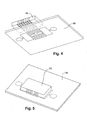
Fig. 4 is a perspective view of the dual LLCC ofFig. 1 oriented above a PCB carrying the circuit traces and solder pads ofFig. 3 ; -
Fig. 5 is a perspective view of the dual LLCC ofFig. 1 in place on the PCB and aligned with the circuit traces ofFig. 4 ; and, -
Fig. 6 is a schematic circuit diagram showing the manner in which the dual LLCC is connected to other circuit components via the mounting arrangement shown inFigs. 1-5 . -
Figures 1 and 2 show an integrated circuit ("IC") 10 that may, for example, be a conventional inertial sensor. TheIC 10 is shown as comprising a so-called dual "leadless chip carrier" ("LLCC") including apackage 12 havingopposing edges conductive IC pins 18. The pins are wire bonded in a known manner to various connection points of the integrated circuit contained in the package, such as inputs, outputs, and power lines. The wire bonded connections are embedded in thepackage 12 and thus not visible in the figures. - Inertial sensors (e.g., single and multiple axis accelerometers, rate sensors, etc.) used in automotive safety systems must be robust against faults. Such inertial sensors are ICs, as for example illustrated in
Figs. 1 and 2 , and are typically mounted to a PCB or other substrate using surface mount technologies. Surface mount technologies can be highly reliable and repeatable. Nonetheless, as explained above, it is possible that solder bridges may inadvertently arise during the soldering process. Failure mode and effects analyses (FMEA) are performed to identify the affects arising from the possible shorting of IC package pins to adjacent pins or to other circuit traces, particularly but not exclusively the power supply lines. With the FMEA in hand, the designer may take steps to avoid, or at least detect and mitigate, possible failure modes. - To add mechanical stability to a component's package, for extended solder life, and to enhance mechanical shock robustness, it is known to place a
center tab 20 on the bottom of the IC for soldering to the PCB. The additional mechanical attachment provided by the center tab will strengthen the physical connection of the IC to the PCB, reduce package mechanical resonances, and also enhance the mechanical and electrical durability of the other solder connections. - The
center tab 20 on theIC 10 is isolated, in the sense that it is not electrically connected within the IC itself to any other element of the packaged circuit. However, the inventors have recognized that the center tab could be electrically connected to something else via the mating solder pad or trace on the PCB. By means of the mating solder pad on the PCB, the center tab could for example be connected electrically to a supply line, such as electrical ground. Alternatively, the solder pad itself could be left electrically floating. - If the
tab 20 were left floating, and a single active pin were to short to the tab, there would be no effect. However, if a second active pin were then also to short to the tab, the two active pins would be effectively shorted together with possibly undesirable consequences. To properly consider and account for such consequences, the FMEA analysis would generally have to evaluate the effects of any pin shorting to any other pin. This analysis and any consequent mitigation actions would be more complicated than just considering potential shorts between adjacent pins. For these reasons, it is undesirable to leave the center tab electrically floating. - If the
center tab 20 is instead soldered to the PCB and is electrically connected to a supply line (e.g., ground, Vdd or Vss) via a circuit trace on the PCB, the possible failure mode permutations are reduced in number and are thus easier to evaluate in a FMEA. Unfortunately, the center tab cannot easily be inspected for a good solder connection to ensure it has been thus electrically connected (e.g., grounded) at the time of manufacture. - According to the present invention, a method and apparatus is provided for ensuring that the
center tab 20 is soldered and electrically connected. In particular, the PCB circuit trace artwork and the IC package are designed so as to form a continuity path that can be tested to confirm continuity and thus verify that a good solder connection between the PCB and thetab 20 has been established. -
Fig. 3 illustrates one example of PCB artwork that, in conjunction with theIC 10 ofFigs. 1 and 2 , would allow such a continuity check. InFig. 3 , the conductive circuit traces are indicated at 30 but the PCB itself is not shown. The area between the traces is, of course, nonconductive. Further, the conductive traces shown in the figure comprise primarily thesolder pads 32 themselves with some additionaldistal length 34; the traces leading from the distal ends of the solder pads to the other components on the PCB (e.g., power supply, microcomputer, etc.) are not shown. - In
Fig. 3 it can be seen that asolder pad 36 is provided for bonding to thecenter tab 20 ofIC 10.Pad 36 has a split configuration, including two pad ends 38 and 40 that are electrically discontinuous; that is, they are separated by anonconductive gap 42. In the embodiment shown inFig. 3 , eachpad end probe landing target IC 10, the two pad ends will be electrically isolated from one another and thus there will be no electrical continuity between them. - The PCB will be populated with the
IC 10 shown inFig. 1 as well as various other electrical components that are not shown in the figures. To this end, solder paste will first be applied to all of the solder pads, including the two pad ends 38 and 40, and theIC 10 will be precision-lowered onto the circuit traces ofFig. 3 , as shown in the representations ofFigs. 4 and 5 . For convenience of description, thePCB 50 is shown in translucent shadow inFigs 4 and 5 . The PCB will then be heated in a conventional manner to melt the paste the solder therein thereby to form the respective solder bonds between the pins of the IC and the pads on the PCB. If the bonds are properly formed, one end of thecenter tab 20 will be soldered topad end 38 and the other end of thecenter tab 20 will be soldered topad end 40, whereby thecenter tab 20 will establish a short between the two solder pad ends and thus electrical continuity between them. - In
Fig. 3 , the rightwardprobe landing target 46 associated withpad end 40 is schematically shown as connected to electrical ground at 48. This is accomplished on the PCB by an additional circuit trace, not shown. Thus, when the IC is properly soldered in place, all of the circuit traces shown inFig. 3 will be grounded, except for the solder pads to which the edge pins ofIC 10 are soldered (although one or more of those pins maybe grounded as well). To confirm solder integrity to the center tab in this embodiment, it is only necessary to check the continuity to ground of theprobe landing target 44. -
Fig. 6 illustrates the electrical connections of the elements described thus far. In the figure, thepins 18 of theIC 10 are connected to respective leads of other components on the PCB such as, for example, a microprocessor orstate machine 58. Atest device 52 has aprobe 54 that may be brought into contact with the probelanding pad end 44. Thetest device 52 provides a test current through thepad end 44, and measures the resulting voltage appearing on the pad end. If good continuity to ground exists, the voltage on thepad 44 will remain zero despite the test current. Thus, a zero voltage reading will indicate that continuity exists and that good solder connections have been formed. Empirical testing can be used to determine the maximum voltage reading that can be expected when good solder connections have been formed. If the test voltage reading is below that maximum voltage, the PCB will be considered to have passed this test. If the test voltage reading is above that maximum voltage, the PCB will be considered to have failed this test. - Various alternatives to the described embodiment are contemplated. It is contemplated, for example, that the continuity check could be done through a different supply voltage line rather than running to electrical ground in the illustrated manner. Also, in place of a dc test voltage, some more sophisticated, time varying signal could be used to measure bond impedance more comprehensively. It is also noted that the continuity check could be performed by circuitry native to the PCB rather than the illustrated external test system. For example, the continuity check could be performed by a host microcomputer during startup of the system or periodically during system runtime, e.g. through a suitable test routine included in the software (firmware) program that is stored in and executed by the microcomputer. Further, the center pad could be divided into any number of segments, rather than merely the illustrated two segments.
- Also, the continuity check function could be implemented directly in the IC itself rather than on the PCB. In this case, the respective functions of the center tab on the IC (shorting bar) and the pad ends on the PCB (continuity test points) will be reversed. In other words, the center tab on the IC will be split into two isolated ends, and the matching solder pad on the PCB will be a single trace. Thus, the solder pad will then short across the two isolated parts of the center tab. The two parts of the center tab will be bonded to circuit elements within the IC that will perform the continuity check between them.
- The mounting arrangement of the present invention permits verification that a sound mechanical and electrical connection is formed between the tab and the PCB. Since the center tab is connected to ground, or alternatively to a supply line voltage, the number of FMEA evaluations that are needed is substantially reduced since an IC pin can only short to an adjacent pin or to the center tab. The FMEA does not have to account for possible shorts of one pin to all other pins as would be needed if the center tab were allowed to electrically float.
- The details of one or more embodiments of the invention are set forth in the accompanying drawings and the description below. Other features, objects, and advantages of the invention will be apparent from the description and drawings, and from the claims.
Claims (15)
- Apparatus for bonding an electrical circuit component onto a substrate, comprising
a first electrically conductive bonding pad fixed to said component,
a second electrically conductive bonding pad fixed to said substrate, wherein one of said first and second bonding pads is divided into at least two parts, with electrical discontinuity between said at least two parts, and
an electrically conductive bond between said first and second bonding pads such that electrical continuity is established from a first part of said one bonding pad, through the other said bonding pad, and through a second part of said one bonding pad,
whereby the integrity of the electrically conductive bond may be evaluated by testing electrical continuity between said first and second parts. - Apparatus as set forth in claim 1, wherein said electrical circuit component includes an integrated circuit having multiple pins for electrical connection to other components on said substrate.
- Apparatus as set forth in claim 2, wherein said first bonding pad is not directly connected to said multiple pins.
- Apparatus as set forth in claim 1, wherein said electrical circuit component includes an inertial sensor having multiple pins for electrical connection to other components on said substrate, and at least one of said other components includes a microprocessor device.
- Apparatus as set forth in claim 4, wherein said inertial sensor is packaged in a leadless chip carrier, said multiple pins are located around the edges of said leadless chip carrier, and said first electrically conductive bonding pad is at least partially located on the bottom surface of said leadless chip carrier between said edges.
- Apparatus as set forth in claim 5, wherein said first electrically conductive bonding pad is a single continuous pad, said second electrically conductive bonding pad is divided into at least two parts with electrical discontinuity between said at least two parts, and wherein each of said at least two parts is soldered to said first electrically conductive bonding pad, whereby electrical continuity is established between said first and second parts through said first electrically conductive bonding pad and the respective solder connections.
- Apparatus as set forth in claim 4, wherein said microprocessor device is programmed to test the electrical continuity between said first and second parts.
- Apparatus as set forth in claim 1, wherein said apparatus further comprises circuit traces adapted for connection to a power source, one of said first and second parts is connected to one of said circuit traces, and the other of said first and second parts is connected to a test landing pad to allow an external tester to check for a good connection from said test landing pad through the first and second electrically conductive bonding pads to said circuit trace.
- Apparatus as set forth in Claim 8, wherein said circuit trace to which said one of said first and second parts is connected to an electrical ground.
- Apparatus as set forth in claim 1, wherein said first electrically conductive bonding pad is split into said first and second parts and further wherein said electrical circuit component includes testing circuitry for testing electrical continuity between said first and second parts.
- Apparatus as set forth in claim 10, wherein said electrical circuit component comprises at least one inertial sensor.
- A method for evaluating the bond between an electrical circuit component and a substrate, comprising the steps of
fixing a first electrically conductive bonding pad to said component, fixing a second electrically conductive bonding pad to said substrate, splitting one of said first and second bonding pads into at least first and second parts so as to have electrical discontinuity between said first and second parts,
forming an electrically conductive bond between said first and second bonding pads such that electrical continuity is established from said first part of said one bonding pad, through the other said bonding pads, and through said second part of said one bonding pad, and
testing electrical continuity between said at least two parts so as to thereby evaluate the integrity of the electrically conductive bond. - A method as set forth in claim 12, wherein the electrical circuit component to which said method is applied is an inertial sensor, and said method further includes the step of forming multiple pins on said inertial sensor for electrical connection to other components on said substrate, and connecting a microprocessor device to said inertial sensor pins.
- A method as set forth in claim 13, wherein the inertial sensor to which said method is applied is packaged in a leadless chip carrier, said step of forming multiple pins on said inertial sensor includes the step of forming multiple pins around the edges of said leadless chip carrier, and wherein said step of fixing said first electrically conductive bonding pad to said component comprises the step of fixing said first electrically conductive bonding pad to said inertial sensor such that said pad is at least partially located on the bottom surface of said leadless chip carrier between said edges, further including the step of testing for short circuits between one of said pins and one of said first and second electrically conductive bonding pads.
- A method as set forth in claim 12, wherein said apparatus further comprises circuit traces adapted for connection to a power source, and wherein said method further comprising the step of connecting said first part to one of said traces and said second part to a test landing pad whereby an external tester may be used to check for a good connection from the test landing pad through the first and second electrically conductive bonding pads to said trace, further comprising the step of connecting an external tester between said landing pad and said trace and checking for a good connection from said test landing pad to said trace with said tester.
Applications Claiming Priority (2)
| Application Number | Priority Date | Filing Date | Title |
|---|---|---|---|
| US201261600867P | 2012-02-20 | 2012-02-20 | |
| US13/716,890 US9635794B2 (en) | 2012-02-20 | 2012-12-17 | Method and apparatus for attachment of integrated circuits |
Publications (3)
| Publication Number | Publication Date |
|---|---|
| EP2629324A2 true EP2629324A2 (en) | 2013-08-21 |
| EP2629324A3 EP2629324A3 (en) | 2016-04-27 |
| EP2629324B1 EP2629324B1 (en) | 2020-07-08 |
Family
ID=47826799
Family Applications (1)
| Application Number | Title | Priority Date | Filing Date |
|---|---|---|---|
| EP13000858.4A Not-in-force EP2629324B1 (en) | 2012-02-20 | 2013-02-20 | Method and apparatus for attachment of a package to a substrate |
Country Status (4)
| Country | Link |
|---|---|
| US (1) | US9635794B2 (en) |
| EP (1) | EP2629324B1 (en) |
| KR (1) | KR101432925B1 (en) |
| CN (1) | CN103337487B (en) |
Families Citing this family (2)
| Publication number | Priority date | Publication date | Assignee | Title |
|---|---|---|---|---|
| TWI598599B (en) * | 2016-02-19 | 2017-09-11 | 啟碁科技股份有限公司 | Dual printed circuit board assembly, printed circuit board and modular printed circuit board |
| JP7815070B2 (en) * | 2022-09-14 | 2026-02-17 | キオクシア株式会社 | Circuit board, semiconductor device, and method for manufacturing the semiconductor device |
Family Cites Families (25)
| Publication number | Priority date | Publication date | Assignee | Title |
|---|---|---|---|---|
| US3718970A (en) * | 1968-11-13 | 1973-03-06 | Vibrionics Res Co | Electromechanical transducer process |
| US5010447A (en) | 1988-12-28 | 1991-04-23 | Texas Instruments Incorporated | Divided capacitor mounting pads |
| KR0154647B1 (en) * | 1995-09-20 | 1998-10-15 | 김광호 | Multi-chip package with exposed common pads |
| JP2825085B2 (en) | 1996-08-29 | 1998-11-18 | 日本電気株式会社 | Semiconductor device mounting structure, mounting board, and mounting state inspection method |
| US6307162B1 (en) | 1996-12-09 | 2001-10-23 | International Business Machines Corporation | Integrated circuit wiring |
| JP2000338129A (en) * | 1999-03-19 | 2000-12-08 | Ngk Insulators Ltd | Sensitivity calibration method for acceleration sensor element |
| US6729176B2 (en) * | 2000-03-31 | 2004-05-04 | Magellan Dis, Inc. | Calibration of orthogonal sensor suite |
| US6546173B2 (en) * | 2001-02-20 | 2003-04-08 | Avanti Optics Corporation | Optical module |
| JP4771245B2 (en) | 2001-04-27 | 2011-09-14 | オプテックス株式会社 | Automatic door sensor |
| WO2005083294A1 (en) * | 2004-03-01 | 2005-09-09 | Nikon Corporation | Pneumatic spring apparatus, vibration-proof apparatus, stage apparatus and exposure apparatus |
| GB2416036A (en) | 2004-07-05 | 2006-01-11 | Richard George Vivian Doble | Electronic device with motion sensor to determine likely impact and protect against damage or to enable the device. |
| JP2006029827A (en) * | 2004-07-12 | 2006-02-02 | Fujitsu Media Device Kk | Inertial sensor |
| US7602050B2 (en) | 2005-07-18 | 2009-10-13 | Qualcomm Incorporated | Integrated circuit packaging |
| US7280370B2 (en) | 2005-08-26 | 2007-10-09 | Delphi Technologies, Inc. | Electronic package and circuit board having segmented contact pads |
| JP5622347B2 (en) * | 2006-08-09 | 2014-11-12 | セイコーエプソン株式会社 | Inertial sensor device |
| US7872483B2 (en) | 2007-12-12 | 2011-01-18 | Samsung Electronics Co., Ltd. | Circuit board having bypass pad |
| KR20090102209A (en) | 2008-03-25 | 2009-09-30 | 서울반도체 주식회사 | Printed circuit board for mounting led there on |
| US8080925B2 (en) * | 2008-09-23 | 2011-12-20 | Custom Sensors & Technologies, Inc. | Inertial sensor with dual cavity package and method of fabrication |
| US20100122565A1 (en) * | 2008-11-15 | 2010-05-20 | Freescale Semiconductor, Inc. | Continuous selftest for inertial sensors at 0 hz |
| US8502151B2 (en) * | 2010-01-31 | 2013-08-06 | Avago Technologies General Ip (Singapore) Pte. Ltd. | Optical proximity sensor package with lead frame |
| US8193620B2 (en) | 2010-02-17 | 2012-06-05 | Analog Devices, Inc. | Integrated circuit package with enlarged die paddle |
| DE102010038453A1 (en) | 2010-07-27 | 2012-02-02 | Robert Bosch Gmbh | solder joint inspection |
| KR101289101B1 (en) * | 2010-11-18 | 2013-07-23 | 삼성전기주식회사 | Inertial Sensor |
| CN202168276U (en) | 2011-07-11 | 2012-03-14 | 深圳崇达多层线路板有限公司 | Interconnectable inner-layer multilayer printed wiring board |
| CN202168278U (en) * | 2011-08-04 | 2012-03-14 | 马夸特开关(上海)有限公司 | Welding structure of circuit board |
-
2012
- 2012-12-17 US US13/716,890 patent/US9635794B2/en not_active Expired - Fee Related
-
2013
- 2013-02-20 EP EP13000858.4A patent/EP2629324B1/en not_active Not-in-force
- 2013-02-20 KR KR1020130018054A patent/KR101432925B1/en not_active Expired - Fee Related
- 2013-02-20 CN CN201310086220.6A patent/CN103337487B/en not_active Expired - Fee Related
Non-Patent Citations (1)
| Title |
|---|
| None |
Also Published As
| Publication number | Publication date |
|---|---|
| CN103337487B (en) | 2016-06-29 |
| CN103337487A (en) | 2013-10-02 |
| EP2629324A3 (en) | 2016-04-27 |
| EP2629324B1 (en) | 2020-07-08 |
| KR101432925B1 (en) | 2014-09-23 |
| US20130215591A1 (en) | 2013-08-22 |
| US9635794B2 (en) | 2017-04-25 |
| KR20130095688A (en) | 2013-08-28 |
Similar Documents
| Publication | Publication Date | Title |
|---|---|---|
| JP4252491B2 (en) | Module with inspection function and inspection method thereof. | |
| US20080158839A1 (en) | Printed Wiring Board, Printed Circuit Board, and Method of Inspecting Joint of Printed Circuit Board | |
| KR101727378B1 (en) | Substrate inspection apparatus | |
| CN102279781B (en) | Method for detecting stability of computer chip, detection device and computer | |
| US8810252B2 (en) | Solder joint inspection | |
| US10073134B2 (en) | Laminate bond strength detection | |
| EP2629324B1 (en) | Method and apparatus for attachment of a package to a substrate | |
| CN103675581B (en) | Electrical connection component and detection method thereof | |
| KR102090578B1 (en) | Substrate of electronic device, electronic device including the same and measuring method of resistance at contact portion | |
| US7280370B2 (en) | Electronic package and circuit board having segmented contact pads | |
| US20120299615A1 (en) | Circuit board assembly and assistant test circuit board | |
| EP2555006B1 (en) | Semiconductor device | |
| CN102967769B (en) | Measurement mechanism with for measuring the method that chip is connected to chip carrier | |
| US8258407B2 (en) | Wiring board and method of preventing high voltage damage | |
| KR20210050292A (en) | Apparatus for testing of pcb and its inspection method | |
| JP2004221574A (en) | Inspection method for mounting / non-mounting of bypass capacitor and through hole disconnection detection method for multilayer board | |
| US7601559B2 (en) | Apparatus and method for identifying proper orientation and electrical conductivity between a semiconductor device and a socket or contactor | |
| JP4982543B2 (en) | Detection method for through-hole breakage in multilayer boards | |
| JP2007315789A (en) | Semiconductor integrated circuit and mounting inspection method thereof | |
| JP2010080770A (en) | Electronic circuit module and method of inspecting the same | |
| JP2008203169A (en) | Semiconductor measuring equipment | |
| US20080088318A1 (en) | Method to test transparent-to-test capacitors | |
| JP2002214274A (en) | Method for inspecting circuit wiring | |
| CN105208764B (en) | The method that circuit board and use circuit board check the configuration status of electronic component | |
| KR20060058521A (en) | Probe card for electronic circuit inspection |
Legal Events
| Date | Code | Title | Description |
|---|---|---|---|
| PUAI | Public reference made under article 153(3) epc to a published international application that has entered the european phase |
Free format text: ORIGINAL CODE: 0009012 |
|
| 17P | Request for examination filed |
Effective date: 20130220 |
|
| AK | Designated contracting states |
Kind code of ref document: A2 Designated state(s): AL AT BE BG CH CY CZ DE DK EE ES FI FR GB GR HR HU IE IS IT LI LT LU LV MC MK MT NL NO PL PT RO RS SE SI SK SM TR |
|
| AX | Request for extension of the european patent |
Extension state: BA ME |
|
| PUAL | Search report despatched |
Free format text: ORIGINAL CODE: 0009013 |
|
| AK | Designated contracting states |
Kind code of ref document: A3 Designated state(s): AL AT BE BG CH CY CZ DE DK EE ES FI FR GB GR HR HU IE IS IT LI LT LU LV MC MK MT NL NO PL PT RO RS SE SI SK SM TR |
|
| AX | Request for extension of the european patent |
Extension state: BA ME |
|
| RIC1 | Information provided on ipc code assigned before grant |
Ipc: H01L 21/66 20060101AFI20160321BHEP Ipc: H05K 1/18 20060101ALI20160321BHEP Ipc: H05K 1/02 20060101ALI20160321BHEP Ipc: H05K 13/04 20060101ALI20160321BHEP |
|
| STAA | Information on the status of an ep patent application or granted ep patent |
Free format text: STATUS: REQUEST FOR EXAMINATION WAS MADE |
|
| R17P | Request for examination filed (corrected) |
Effective date: 20130220 |
|
| RBV | Designated contracting states (corrected) |
Designated state(s): AL AT BE BG CH CY CZ DE DK EE ES FI FR GB GR HR HU IE IS IT LI LT LU LV MC MK MT NL NO PL PT RO RS SE SI SK SM TR |
|
| R17P | Request for examination filed (corrected) |
Effective date: 20130220 |
|
| STAA | Information on the status of an ep patent application or granted ep patent |
Free format text: STATUS: EXAMINATION IS IN PROGRESS |
|
| 17Q | First examination report despatched |
Effective date: 20170905 |
|
| GRAP | Despatch of communication of intention to grant a patent |
Free format text: ORIGINAL CODE: EPIDOSNIGR1 |
|
| STAA | Information on the status of an ep patent application or granted ep patent |
Free format text: STATUS: GRANT OF PATENT IS INTENDED |
|
| INTG | Intention to grant announced |
Effective date: 20200228 |
|
| GRAS | Grant fee paid |
Free format text: ORIGINAL CODE: EPIDOSNIGR3 |
|
| GRAA | (expected) grant |
Free format text: ORIGINAL CODE: 0009210 |
|
| STAA | Information on the status of an ep patent application or granted ep patent |
Free format text: STATUS: THE PATENT HAS BEEN GRANTED |
|
| AK | Designated contracting states |
Kind code of ref document: B1 Designated state(s): AL AT BE BG CH CY CZ DE DK EE ES FI FR GB GR HR HU IE IS IT LI LT LU LV MC MK MT NL NO PL PT RO RS SE SI SK SM TR |
|
| REG | Reference to a national code |
Ref country code: GB Ref legal event code: FG4D |
|
| REG | Reference to a national code |
Ref country code: AT Ref legal event code: REF Ref document number: 1289375 Country of ref document: AT Kind code of ref document: T Effective date: 20200715 Ref country code: CH Ref legal event code: EP |
|
| REG | Reference to a national code |
Ref country code: DE Ref legal event code: R096 Ref document number: 602013070442 Country of ref document: DE |
|
| REG | Reference to a national code |
Ref country code: IE Ref legal event code: FG4D |
|
| REG | Reference to a national code |
Ref country code: LT Ref legal event code: MG4D |
|
| REG | Reference to a national code |
Ref country code: AT Ref legal event code: MK05 Ref document number: 1289375 Country of ref document: AT Kind code of ref document: T Effective date: 20200708 |
|
| REG | Reference to a national code |
Ref country code: NL Ref legal event code: MP Effective date: 20200708 |
|
| PG25 | Lapsed in a contracting state [announced via postgrant information from national office to epo] |
Ref country code: GR Free format text: LAPSE BECAUSE OF FAILURE TO SUBMIT A TRANSLATION OF THE DESCRIPTION OR TO PAY THE FEE WITHIN THE PRESCRIBED TIME-LIMIT Effective date: 20201009 Ref country code: NO Free format text: LAPSE BECAUSE OF FAILURE TO SUBMIT A TRANSLATION OF THE DESCRIPTION OR TO PAY THE FEE WITHIN THE PRESCRIBED TIME-LIMIT Effective date: 20201008 Ref country code: FI Free format text: LAPSE BECAUSE OF FAILURE TO SUBMIT A TRANSLATION OF THE DESCRIPTION OR TO PAY THE FEE WITHIN THE PRESCRIBED TIME-LIMIT Effective date: 20200708 Ref country code: LT Free format text: LAPSE BECAUSE OF FAILURE TO SUBMIT A TRANSLATION OF THE DESCRIPTION OR TO PAY THE FEE WITHIN THE PRESCRIBED TIME-LIMIT Effective date: 20200708 Ref country code: ES Free format text: LAPSE BECAUSE OF FAILURE TO SUBMIT A TRANSLATION OF THE DESCRIPTION OR TO PAY THE FEE WITHIN THE PRESCRIBED TIME-LIMIT Effective date: 20200708 Ref country code: SE Free format text: LAPSE BECAUSE OF FAILURE TO SUBMIT A TRANSLATION OF THE DESCRIPTION OR TO PAY THE FEE WITHIN THE PRESCRIBED TIME-LIMIT Effective date: 20200708 Ref country code: AT Free format text: LAPSE BECAUSE OF FAILURE TO SUBMIT A TRANSLATION OF THE DESCRIPTION OR TO PAY THE FEE WITHIN THE PRESCRIBED TIME-LIMIT Effective date: 20200708 Ref country code: BG Free format text: LAPSE BECAUSE OF FAILURE TO SUBMIT A TRANSLATION OF THE DESCRIPTION OR TO PAY THE FEE WITHIN THE PRESCRIBED TIME-LIMIT Effective date: 20201008 Ref country code: PT Free format text: LAPSE BECAUSE OF FAILURE TO SUBMIT A TRANSLATION OF THE DESCRIPTION OR TO PAY THE FEE WITHIN THE PRESCRIBED TIME-LIMIT Effective date: 20201109 Ref country code: HR Free format text: LAPSE BECAUSE OF FAILURE TO SUBMIT A TRANSLATION OF THE DESCRIPTION OR TO PAY THE FEE WITHIN THE PRESCRIBED TIME-LIMIT Effective date: 20200708 |
|
| PG25 | Lapsed in a contracting state [announced via postgrant information from national office to epo] |
Ref country code: IS Free format text: LAPSE BECAUSE OF FAILURE TO SUBMIT A TRANSLATION OF THE DESCRIPTION OR TO PAY THE FEE WITHIN THE PRESCRIBED TIME-LIMIT Effective date: 20201108 Ref country code: PL Free format text: LAPSE BECAUSE OF FAILURE TO SUBMIT A TRANSLATION OF THE DESCRIPTION OR TO PAY THE FEE WITHIN THE PRESCRIBED TIME-LIMIT Effective date: 20200708 Ref country code: RS Free format text: LAPSE BECAUSE OF FAILURE TO SUBMIT A TRANSLATION OF THE DESCRIPTION OR TO PAY THE FEE WITHIN THE PRESCRIBED TIME-LIMIT Effective date: 20200708 Ref country code: LV Free format text: LAPSE BECAUSE OF FAILURE TO SUBMIT A TRANSLATION OF THE DESCRIPTION OR TO PAY THE FEE WITHIN THE PRESCRIBED TIME-LIMIT Effective date: 20200708 |
|
| PG25 | Lapsed in a contracting state [announced via postgrant information from national office to epo] |
Ref country code: NL Free format text: LAPSE BECAUSE OF FAILURE TO SUBMIT A TRANSLATION OF THE DESCRIPTION OR TO PAY THE FEE WITHIN THE PRESCRIBED TIME-LIMIT Effective date: 20200708 |
|
| REG | Reference to a national code |
Ref country code: DE Ref legal event code: R097 Ref document number: 602013070442 Country of ref document: DE |
|
| PG25 | Lapsed in a contracting state [announced via postgrant information from national office to epo] |
Ref country code: EE Free format text: LAPSE BECAUSE OF FAILURE TO SUBMIT A TRANSLATION OF THE DESCRIPTION OR TO PAY THE FEE WITHIN THE PRESCRIBED TIME-LIMIT Effective date: 20200708 Ref country code: CZ Free format text: LAPSE BECAUSE OF FAILURE TO SUBMIT A TRANSLATION OF THE DESCRIPTION OR TO PAY THE FEE WITHIN THE PRESCRIBED TIME-LIMIT Effective date: 20200708 Ref country code: DK Free format text: LAPSE BECAUSE OF FAILURE TO SUBMIT A TRANSLATION OF THE DESCRIPTION OR TO PAY THE FEE WITHIN THE PRESCRIBED TIME-LIMIT Effective date: 20200708 Ref country code: IT Free format text: LAPSE BECAUSE OF FAILURE TO SUBMIT A TRANSLATION OF THE DESCRIPTION OR TO PAY THE FEE WITHIN THE PRESCRIBED TIME-LIMIT Effective date: 20200708 Ref country code: RO Free format text: LAPSE BECAUSE OF FAILURE TO SUBMIT A TRANSLATION OF THE DESCRIPTION OR TO PAY THE FEE WITHIN THE PRESCRIBED TIME-LIMIT Effective date: 20200708 Ref country code: SM Free format text: LAPSE BECAUSE OF FAILURE TO SUBMIT A TRANSLATION OF THE DESCRIPTION OR TO PAY THE FEE WITHIN THE PRESCRIBED TIME-LIMIT Effective date: 20200708 |
|
| PGFP | Annual fee paid to national office [announced via postgrant information from national office to epo] |
Ref country code: FR Payment date: 20210223 Year of fee payment: 9 |
|
| PLBE | No opposition filed within time limit |
Free format text: ORIGINAL CODE: 0009261 |
|
| STAA | Information on the status of an ep patent application or granted ep patent |
Free format text: STATUS: NO OPPOSITION FILED WITHIN TIME LIMIT |
|
| PG25 | Lapsed in a contracting state [announced via postgrant information from national office to epo] |
Ref country code: AL Free format text: LAPSE BECAUSE OF FAILURE TO SUBMIT A TRANSLATION OF THE DESCRIPTION OR TO PAY THE FEE WITHIN THE PRESCRIBED TIME-LIMIT Effective date: 20200708 |
|
| PGFP | Annual fee paid to national office [announced via postgrant information from national office to epo] |
Ref country code: DE Payment date: 20210225 Year of fee payment: 9 Ref country code: GB Payment date: 20210225 Year of fee payment: 9 |
|
| 26N | No opposition filed |
Effective date: 20210409 |
|
| PG25 | Lapsed in a contracting state [announced via postgrant information from national office to epo] |
Ref country code: SK Free format text: LAPSE BECAUSE OF FAILURE TO SUBMIT A TRANSLATION OF THE DESCRIPTION OR TO PAY THE FEE WITHIN THE PRESCRIBED TIME-LIMIT Effective date: 20200708 |
|
| PG25 | Lapsed in a contracting state [announced via postgrant information from national office to epo] |
Ref country code: SI Free format text: LAPSE BECAUSE OF FAILURE TO SUBMIT A TRANSLATION OF THE DESCRIPTION OR TO PAY THE FEE WITHIN THE PRESCRIBED TIME-LIMIT Effective date: 20200708 |
|
| PG25 | Lapsed in a contracting state [announced via postgrant information from national office to epo] |
Ref country code: MC Free format text: LAPSE BECAUSE OF FAILURE TO SUBMIT A TRANSLATION OF THE DESCRIPTION OR TO PAY THE FEE WITHIN THE PRESCRIBED TIME-LIMIT Effective date: 20200708 |
|
| REG | Reference to a national code |
Ref country code: BE Ref legal event code: MM Effective date: 20210228 |
|
| PG25 | Lapsed in a contracting state [announced via postgrant information from national office to epo] |
Ref country code: CH Free format text: LAPSE BECAUSE OF NON-PAYMENT OF DUE FEES Effective date: 20210228 Ref country code: LU Free format text: LAPSE BECAUSE OF NON-PAYMENT OF DUE FEES Effective date: 20210220 Ref country code: LI Free format text: LAPSE BECAUSE OF NON-PAYMENT OF DUE FEES Effective date: 20210228 |
|
| PG25 | Lapsed in a contracting state [announced via postgrant information from national office to epo] |
Ref country code: IE Free format text: LAPSE BECAUSE OF NON-PAYMENT OF DUE FEES Effective date: 20210220 |
|
| PG25 | Lapsed in a contracting state [announced via postgrant information from national office to epo] |
Ref country code: BE Free format text: LAPSE BECAUSE OF NON-PAYMENT OF DUE FEES Effective date: 20210228 |
|
| REG | Reference to a national code |
Ref country code: DE Ref legal event code: R119 Ref document number: 602013070442 Country of ref document: DE |
|
| GBPC | Gb: european patent ceased through non-payment of renewal fee |
Effective date: 20220220 |
|
| PG25 | Lapsed in a contracting state [announced via postgrant information from national office to epo] |
Ref country code: FR Free format text: LAPSE BECAUSE OF NON-PAYMENT OF DUE FEES Effective date: 20220228 |
|
| PG25 | Lapsed in a contracting state [announced via postgrant information from national office to epo] |
Ref country code: GB Free format text: LAPSE BECAUSE OF NON-PAYMENT OF DUE FEES Effective date: 20220220 Ref country code: DE Free format text: LAPSE BECAUSE OF NON-PAYMENT OF DUE FEES Effective date: 20220901 |
|
| PG25 | Lapsed in a contracting state [announced via postgrant information from national office to epo] |
Ref country code: HU Free format text: LAPSE BECAUSE OF FAILURE TO SUBMIT A TRANSLATION OF THE DESCRIPTION OR TO PAY THE FEE WITHIN THE PRESCRIBED TIME-LIMIT; INVALID AB INITIO Effective date: 20130220 |
|
| PG25 | Lapsed in a contracting state [announced via postgrant information from national office to epo] |
Ref country code: CY Free format text: LAPSE BECAUSE OF FAILURE TO SUBMIT A TRANSLATION OF THE DESCRIPTION OR TO PAY THE FEE WITHIN THE PRESCRIBED TIME-LIMIT Effective date: 20200708 |
|
| PG25 | Lapsed in a contracting state [announced via postgrant information from national office to epo] |
Ref country code: MK Free format text: LAPSE BECAUSE OF FAILURE TO SUBMIT A TRANSLATION OF THE DESCRIPTION OR TO PAY THE FEE WITHIN THE PRESCRIBED TIME-LIMIT Effective date: 20200708 |
|
| PG25 | Lapsed in a contracting state [announced via postgrant information from national office to epo] |
Ref country code: MT Free format text: LAPSE BECAUSE OF FAILURE TO SUBMIT A TRANSLATION OF THE DESCRIPTION OR TO PAY THE FEE WITHIN THE PRESCRIBED TIME-LIMIT Effective date: 20200708 |
|
| PG25 | Lapsed in a contracting state [announced via postgrant information from national office to epo] |
Ref country code: TR Free format text: LAPSE BECAUSE OF FAILURE TO SUBMIT A TRANSLATION OF THE DESCRIPTION OR TO PAY THE FEE WITHIN THE PRESCRIBED TIME-LIMIT Effective date: 20200708 |