EP2629304A1 - Flexible conductive material and transducer, flexible circuit board, and electromagnetic shield using said flexible conductive material - Google Patents
Flexible conductive material and transducer, flexible circuit board, and electromagnetic shield using said flexible conductive material Download PDFInfo
- Publication number
- EP2629304A1 EP2629304A1 EP11832562.0A EP11832562A EP2629304A1 EP 2629304 A1 EP2629304 A1 EP 2629304A1 EP 11832562 A EP11832562 A EP 11832562A EP 2629304 A1 EP2629304 A1 EP 2629304A1
- Authority
- EP
- European Patent Office
- Prior art keywords
- conductive material
- dielectric film
- flexible conductive
- flexible
- electrodes
- Prior art date
- Legal status (The legal status is an assumption and is not a legal conclusion. Google has not performed a legal analysis and makes no representation as to the accuracy of the status listed.)
- Withdrawn
Links
Images





Classifications
-
- H—ELECTRICITY
- H01—ELECTRIC ELEMENTS
- H01B—CABLES; CONDUCTORS; INSULATORS; SELECTION OF MATERIALS FOR THEIR CONDUCTIVE, INSULATING OR DIELECTRIC PROPERTIES
- H01B1/00—Conductors or conductive bodies characterised by the conductive materials; Selection of materials as conductors
- H01B1/20—Conductive material dispersed in non-conductive organic material
-
- H—ELECTRICITY
- H01—ELECTRIC ELEMENTS
- H01B—CABLES; CONDUCTORS; INSULATORS; SELECTION OF MATERIALS FOR THEIR CONDUCTIVE, INSULATING OR DIELECTRIC PROPERTIES
- H01B1/00—Conductors or conductive bodies characterised by the conductive materials; Selection of materials as conductors
- H01B1/20—Conductive material dispersed in non-conductive organic material
- H01B1/22—Conductive material dispersed in non-conductive organic material the conductive material comprising metals or alloys
-
- C—CHEMISTRY; METALLURGY
- C08—ORGANIC MACROMOLECULAR COMPOUNDS; THEIR PREPARATION OR CHEMICAL WORKING-UP; COMPOSITIONS BASED THEREON
- C08K—Use of inorganic or non-macromolecular organic substances as compounding ingredients
- C08K3/00—Use of inorganic substances as compounding ingredients
- C08K3/02—Elements
- C08K3/04—Carbon
-
- H—ELECTRICITY
- H01—ELECTRIC ELEMENTS
- H01B—CABLES; CONDUCTORS; INSULATORS; SELECTION OF MATERIALS FOR THEIR CONDUCTIVE, INSULATING OR DIELECTRIC PROPERTIES
- H01B1/00—Conductors or conductive bodies characterised by the conductive materials; Selection of materials as conductors
- H01B1/20—Conductive material dispersed in non-conductive organic material
- H01B1/24—Conductive material dispersed in non-conductive organic material the conductive material comprising carbon-silicon compounds, carbon or silicon
-
- H—ELECTRICITY
- H01—ELECTRIC ELEMENTS
- H01B—CABLES; CONDUCTORS; INSULATORS; SELECTION OF MATERIALS FOR THEIR CONDUCTIVE, INSULATING OR DIELECTRIC PROPERTIES
- H01B5/00—Non-insulated conductors or conductive bodies characterised by their form
- H01B5/14—Non-insulated conductors or conductive bodies characterised by their form comprising conductive layers or films on insulating-supports
-
- H—ELECTRICITY
- H01—ELECTRIC ELEMENTS
- H01R—ELECTRICALLY-CONDUCTIVE CONNECTIONS; STRUCTURAL ASSOCIATIONS OF A PLURALITY OF MUTUALLY-INSULATED ELECTRICAL CONNECTING ELEMENTS; COUPLING DEVICES; CURRENT COLLECTORS
- H01R11/00—Individual connecting elements providing two or more spaced connecting locations for conductive members which are, or may be, thereby interconnected, e.g. end pieces for wires or cables supported by the wire or cable and having means for facilitating electrical connection to some other wire, terminal, or conductive member, blocks of binding posts
- H01R11/01—Individual connecting elements providing two or more spaced connecting locations for conductive members which are, or may be, thereby interconnected, e.g. end pieces for wires or cables supported by the wire or cable and having means for facilitating electrical connection to some other wire, terminal, or conductive member, blocks of binding posts characterised by the form or arrangement of the conductive interconnection between the connecting locations
-
- H—ELECTRICITY
- H02—GENERATION; CONVERSION OR DISTRIBUTION OF ELECTRIC POWER
- H02N—ELECTRIC MACHINES NOT OTHERWISE PROVIDED FOR
- H02N1/00—Electrostatic generators or motors using a solid moving electrostatic charge carrier
-
- H—ELECTRICITY
- H05—ELECTRIC TECHNIQUES NOT OTHERWISE PROVIDED FOR
- H05K—PRINTED CIRCUITS; CASINGS OR CONSTRUCTIONAL DETAILS OF ELECTRIC APPARATUS; MANUFACTURE OF ASSEMBLAGES OF ELECTRICAL COMPONENTS
- H05K1/00—Printed circuits
- H05K1/02—Details
- H05K1/03—Use of materials for the substrate
- H05K1/0313—Organic insulating material
- H05K1/0353—Organic insulating material consisting of two or more materials, e.g. two or more polymers, polymer + filler, + reinforcement
- H05K1/0373—Organic insulating material consisting of two or more materials, e.g. two or more polymers, polymer + filler, + reinforcement containing additives, e.g. fillers
-
- H—ELECTRICITY
- H10—SEMICONDUCTOR DEVICES; ELECTRIC SOLID-STATE DEVICES NOT OTHERWISE PROVIDED FOR
- H10N—ELECTRIC SOLID-STATE DEVICES NOT OTHERWISE PROVIDED FOR
- H10N30/00—Piezoelectric or electrostrictive devices
- H10N30/704—Piezoelectric or electrostrictive devices based on piezoelectric or electrostrictive films or coatings
-
- H—ELECTRICITY
- H10—SEMICONDUCTOR DEVICES; ELECTRIC SOLID-STATE DEVICES NOT OTHERWISE PROVIDED FOR
- H10N—ELECTRIC SOLID-STATE DEVICES NOT OTHERWISE PROVIDED FOR
- H10N30/00—Piezoelectric or electrostrictive devices
- H10N30/80—Constructional details
- H10N30/87—Electrodes or interconnections, e.g. leads or terminals
- H10N30/877—Conductive materials
- H10N30/878—Conductive materials the principal material being non-metallic, e.g. oxide or carbon based
-
- H—ELECTRICITY
- H05—ELECTRIC TECHNIQUES NOT OTHERWISE PROVIDED FOR
- H05K—PRINTED CIRCUITS; CASINGS OR CONSTRUCTIONAL DETAILS OF ELECTRIC APPARATUS; MANUFACTURE OF ASSEMBLAGES OF ELECTRICAL COMPONENTS
- H05K1/00—Printed circuits
- H05K1/02—Details
- H05K1/0213—Electrical arrangements not otherwise provided for
- H05K1/0254—High voltage adaptations; Electrical insulation details; Overvoltage or electrostatic discharge protection ; Arrangements for regulating voltages or for using plural voltages
- H05K1/0256—Electrical insulation details, e.g. around high voltage areas
-
- H—ELECTRICITY
- H05—ELECTRIC TECHNIQUES NOT OTHERWISE PROVIDED FOR
- H05K—PRINTED CIRCUITS; CASINGS OR CONSTRUCTIONAL DETAILS OF ELECTRIC APPARATUS; MANUFACTURE OF ASSEMBLAGES OF ELECTRICAL COMPONENTS
- H05K1/00—Printed circuits
- H05K1/16—Printed circuits incorporating printed electric components, e.g. printed resistors, capacitors or inductors
- H05K1/162—Printed circuits incorporating printed electric components, e.g. printed resistors, capacitors or inductors incorporating printed capacitors
-
- H—ELECTRICITY
- H05—ELECTRIC TECHNIQUES NOT OTHERWISE PROVIDED FOR
- H05K—PRINTED CIRCUITS; CASINGS OR CONSTRUCTIONAL DETAILS OF ELECTRIC APPARATUS; MANUFACTURE OF ASSEMBLAGES OF ELECTRICAL COMPONENTS
- H05K2201/00—Indexing scheme relating to printed circuits covered by H05K1/00
- H05K2201/01—Dielectrics
- H05K2201/0104—Properties and characteristics in general
- H05K2201/0133—Elastomeric or compliant polymer
-
- H—ELECTRICITY
- H05—ELECTRIC TECHNIQUES NOT OTHERWISE PROVIDED FOR
- H05K—PRINTED CIRCUITS; CASINGS OR CONSTRUCTIONAL DETAILS OF ELECTRIC APPARATUS; MANUFACTURE OF ASSEMBLAGES OF ELECTRICAL COMPONENTS
- H05K2201/00—Indexing scheme relating to printed circuits covered by H05K1/00
- H05K2201/03—Conductive materials
- H05K2201/032—Materials
- H05K2201/0323—Carbon
-
- H—ELECTRICITY
- H10—SEMICONDUCTOR DEVICES; ELECTRIC SOLID-STATE DEVICES NOT OTHERWISE PROVIDED FOR
- H10N—ELECTRIC SOLID-STATE DEVICES NOT OTHERWISE PROVIDED FOR
- H10N30/00—Piezoelectric or electrostrictive devices
- H10N30/20—Piezoelectric or electrostrictive devices with electrical input and mechanical output, e.g. functioning as actuators or vibrators
- H10N30/206—Piezoelectric or electrostrictive devices with electrical input and mechanical output, e.g. functioning as actuators or vibrators using only longitudinal or thickness displacement, e.g. d33 or d31 type devices
-
- H—ELECTRICITY
- H10—SEMICONDUCTOR DEVICES; ELECTRIC SOLID-STATE DEVICES NOT OTHERWISE PROVIDED FOR
- H10N—ELECTRIC SOLID-STATE DEVICES NOT OTHERWISE PROVIDED FOR
- H10N30/00—Piezoelectric or electrostrictive devices
- H10N30/30—Piezoelectric or electrostrictive devices with mechanical input and electrical output, e.g. functioning as generators or sensors
-
- H—ELECTRICITY
- H10—SEMICONDUCTOR DEVICES; ELECTRIC SOLID-STATE DEVICES NOT OTHERWISE PROVIDED FOR
- H10N—ELECTRIC SOLID-STATE DEVICES NOT OTHERWISE PROVIDED FOR
- H10N30/00—Piezoelectric or electrostrictive devices
- H10N30/80—Constructional details
- H10N30/85—Piezoelectric or electrostrictive active materials
- H10N30/857—Macromolecular compositions
Definitions
- the present invention relates to a flexible conductive material which is favorable for an extendable and contractible electrode, a wiring, and the like, and to a transducer, a flexible wiring board, and an electromagnetic shield using the same.
- a transducer examples include an actuator in which a pair of electrodes is disposed on both a front and back surface of a dielectric film made from an elastomer (see, for example, Patent Documents 1 and 2).
- an actuator of this type when the applied voltage between the electrodes is increased, an electrostatic attraction between the electrodes increases. Therefore, the dielectric film sandwiched between the electrodes is compressed in a thickness direction and the thickness of the dielectric film decreases. When the film thickness decreases, the dielectric film proportionally extends in a horizontal direction with respect to the electrode surfaces.
- the actuator drives drive target members by extension and contraction of the dielectric film in response to the magnitude of the applied voltage.
- the electrodes are affixed to both the front and back surfaces of the dielectric film. Accordingly, the electrodes must be extendable and contractible in response to deformation of the dielectric film so as not to interfere with the extension and contraction thereof.
- the extendable and contractible electrodes can, for example and as disclosed in Patent Document 2, be formed from a flexible conductive material in which a conductive agent such as carbon black is included in an elastomer.
- a conductive agent such as carbon black
- impurities in the elastomer are a negative feature.
- unreacted sulfur, vulcanization accelerators, and the like as well as products (reaction residue) of sulfur, vulcanization accelerators, and the like commonly remain in the elastomer after cross-linking.
- reaction residues such as initiators, emulsifiers, and chain transfer agents added during a polymerization reaction.
- reaction residues are impurities in the elastomer. Accordingly, when an electrode is formed on a surface of a dielectric film from a flexible conductive material containing the elastomer described above, there is a possibility that impurities in the electrode (flexible conductive material) may ionize and transfer to the dielectric film. Further, in a case where a metallic powder (e.g., silver powder) is used as the conductive agent, there is a possibility that ionized silver (Ag + ) may transfer to the dielectric film and be deposited as silver (migration).
- a metallic powder e.g., silver powder
- impurities contained in a member (such as a dielectric film) touching the flexible conductive material may, after transferring to the flexible conductive material, transfer once more to the member.
- impurities may be, for example, zinc salt and iron salt of dimethyldithiocarbamate used as a cross-linking promoter; sodium salt and zinc salt of 2-mercaptobenzothiazole; hydrolysate of an organic phosphate compound of tricresylphosphate and the like used as a plasticizer and fire retardant; quaternary ammonium salt derived from a surfactant; and various other metallic ions (Na + , K + , Mg 2+ ) contained in trace amounts.
- the influence of impurities contained in the member touching the flexible conductive material cannot be ignored.
- the transfer of impurities is also a negative feature in sensors, power generating elements, and the like in which electrodes are disposed with a dielectric film therebetween. Further, the transfer of impurities also becomes a negative feature in a case where wiring and the like is formed on a surface of an elastic base material such as an elastomer, the wiring and the like being formed from a flexible conductive material containing an elastomer. Specifically, due to the transfer of impurities from the flexible conductive material to the elastic base material, there is a possibility that electrical resistance of the elastic base material may be reduced and leakage current may occur.
- the present invention is conceived in light of such conditions, and has as its purpose to provide a flexible conductive material in which the transfer of impurities to an adherend such as a dielectric film is reduced. Further, the present invention has as its purpose to provide a transducer and a flexible wiring board having a small leakage current and excellent durability by forming an electrode and a wiring from the flexible conductive material. Further, the present invention has as its purpose to provide an electromagnetic shield having a small leakage current using the flexible conductive material.
- a flexible conductive material of the present invention includes an elastomer, a conductive agent filled in the elastomer, and an adsorbent fixed inside the elastomer and able to adsorb ionic material.
- the adsorbent is incorporated into the flexible conductive material of the present invention.
- the adsorbent is able to adsorb ionic material.
- the adsorbent can adsorb impurities that have ionized within the elastomer.
- the adsorbent is fixed inside the elastomer. Therefore, the impurities adsorbed to the adsorbent stay inside the elastomer and do not transfer from the elastomer to the exterior (to another member touching the flexible conductive material).
- the adsorbent preferably does not transfer from inside the cross-linked structure (polymer network) of the elastomer to the exterior. Therefore, the adsorbent and the elastomer may be either chemically bonded or not.
- ionized impurities are unlikely to transfer to another member touching the flexible conductive material. Further, even when an ionized impurity is transferred thereto from the other members touching the flexible conductive material of the present invention, the impurity can be inhibited from transferring once more to the other members. Therefore, in a case where an electrode is formed from the flexible conductive material of the present invention to configure a transducer for an actuator or the like, few impurities transfer from the electrode to the dielectric film. Thus, electrical resistance of the dielectric film is unlikely to be reduced. That is, during application of voltage, electric current is unlikely to flow through the dielectric film.
- a transducer of the present invention includes a dielectric film made of an elastomer, a plurality of electrodes disposed with the dielectric film therebetween, and a wiring connecting each of the plurality of electrodes. At least one of the electrodes and the wiring is configured with the flexible conductive material of the present invention.
- the transducer is an apparatus converting energy of a certain type into energy of another type.
- the transducer contains an actuator, a sensor, a power generating element, and the like converting mechanical energy into electrical energy; alternatively, the transducer contains a speaker, a microphone, and the like converting acoustic energy into electrical energy.
- the transducer of the present invention at least one of the electrodes and the wiring (referred to "electrodes and the like" hereafter, where appropriate) is formed from the flexible conductive material of the present invention described above. Accordingly, when the dielectric film deforms, the electrodes and the like extend and contract to follow the deformation. Therefore, the movement of the dielectric film is unlikely to be impeded. Further, few impurities transfer from the electrodes and the like to the dielectric film. Therefore, the possibility is low that the electrical resistance of the dielectric film will be reduced. Accordingly, during application of voltage, electric current is unlikely to flow through the dielectric film. That is, the possibility is low that the physical properties of the dielectric film will change or that the dielectric film will break due to heat. Accordingly, the transducer of the present invention has excellent durability. Further, when the transducer of the present invention is used as an actuator, a large voltage can be applied to the dielectric film. Accordingly, greater power can be generated by increasing the applied voltage.
- a flexible wiring board of the present invention includes an elastic base material and a wiring disposed on a surface of the elastic base material. At least a portion of the wiring is configured with the flexible conductive material of the present invention described above.
- the wiring extends and contracts to follow deformation of the elastic base material. Accordingly, the flexible wiring board of the present invention is favorable as wiring for movable components and components having a complex shape. Further, few impurities transfer from the wiring to the elastic base material. Therefore, the possibility is low that the electrical resistance of the elastic base material will be reduced and that electric current will flow into the elastic base material. Therefore, a malfunction is inhibited. Further, the possibility is low that the physical properties of the elastic base material will change and that the elastic base material will break due to Joule heating. In this way, the flexible wiring board of the present invention has excellent durability.
- An electromagnetic shield of the present invention is configured with the flexible conductive material of the present invention.
- the flexible conductive material of the present invention can be manufactured from a coating material in which a raw material such as a rubber polymer is dissolved in a predetermined solvent.
- the flexible conductive material of the present invention can be formed in various shapes from a kneaded raw material. Therefore, the flexible conductive material of the present invention is easily disposed as an electromagnetic shield in various positions where shielding from electromagnetic waves is desired.
- impurities in the electromagnetic shield are unlikely to transfer to a member touching the electromagnetic shield. Therefore, the possibility is low that the electrical resistance of the touching member will be reduced, and that leakage current will occur. Accordingly, the possibility is low that the physical properties of the touching member will change and that the member will break due to Joule heating.
- actuator transducer
- 10 dielectric film
- 11a and 11b electrode
- 12a and 12b wiring
- 13 power source
- 14a and 14b electrode
- 140a and 140b inner conductive layer
- 141a and 141b outer conductive layer
- 2 capacitance-type sensor (transducer)
- 20 dielectric film
- 21a and 21b electrode
- 22a and 22b wiring
- 23a and 23b cover film
- 24 connector.
- power generating element transducer
- 30 dielectric film
- 31a and 31b electrode
- 32a - 32c wiring.
- 4 speaker (transducer); 40a: first outer frame; 40b: second outer frame; 41a: first inner frame; 41b: second inner frame; 42a: first dielectric film; 42b: second dielectric film; 43a: first outer electrode; 43b: second outer electrode; 44a: first inner electrode; 44b: second inner electrode; 45a: first vibration plate; 45b: second vibration plate; 430a, 430b, 440a, and 440b: terminal; 460: bolt; 461: nut; 462: spacer.
- 5A first element for testing; 5B: second element for testing; 50: dielectric film; 51a and 51b: electrode; 52: upper chuck; 53: lower chuck; 54a and 54b: inner electrode; 55a and 55b: outer electrode.
- 6 flexible wiring board; 60: elastic base material; 61: connector for front wiring; 62: connector for back wiring; 01X - 16X: front electrode; 01Y - 16Y: back electrode; 01x - 16x: front wiring; 01y - 16y: back wiring.
- the flexible conductive material of the present invention includes an elastomer, a conductive agent, and an adsorbent.
- the type of the elastomer is not particularly limited. In a case where the flexible conductive material is used for an electrode and a wiring of the transducer which includes a dielectric film made of an elastomer, from the perspective of being flexible and easily extended and contracted, an elastomer having an elastic modulus of 10 MPa or less is preferably used.
- Examples include silicone rubber, ethylene-propylene copolymerized rubber, natural rubber, styrene-butadiene copolymerized rubber, acrylonitrile-butadiene rubber (NBR), hydrogenated acrylonitrile-butadiene rubber (H-NBR), acrylic rubber, epichlorohydrin rubber, chlorosulfonated polyethylene, chlorinated polyethylene, urethane rubber, and a polyurethane series thermoplastic elastomer.
- NBR acrylonitrile-butadiene rubber
- H-NBR hydrogenated acrylonitrile-butadiene rubber
- acrylic rubber epichlorohydrin rubber
- chlorosulfonated polyethylene chlorinated polyethylene
- urethane rubber urethane rubber
- a polyurethane series thermoplastic elastomer an elastomer modified by the introduction of a functional group and the like may also be used.
- an elastomer one kind can be used alone or, alternatively, two
- the adsorbent When the adsorbent is chemically bonded to the elastomer, the adsorbent can be reliably fixed inside the elastomer. Accordingly, as the elastomer, an elastomer having a functional group and structure capable of reacting with the adsorbent is preferred. For example, as the adsorbent, when a compound having a mercapto group is used, an elastomer is favorable having a functional group and structure capable of reacting with the mercapto group or, alternatively, with another functional group in the compound.
- the conductive agent is not particularly limited.
- the conductive agent may be appropriately selected from among carbon materials such as carbon black, carbon nanotubes, and graphite; metallic materials such as silver, gold, copper, nickel, rhodium, palladium, chrome, titanium, platinum, iron, and metal alloys thereof; and conductive oxides such as indium tin oxide (ITO) and a conductive oxide in which titanium oxide and zinc oxide are doped with another metal such as aluminum and antimony.
- One kind of conductive agent may be used alone, and two or more kinds of conductive agent may also be mixed for use.
- carbon black is favorable for having a high degree of adhesion with a parent material elastomer and for easily aggregating to form conductive pathways.
- highly conductive carbon blacks such as Ketjen Black and conductive agents which are highly adsorptive of impurities and have fine holes, such as activated carbon and mesoporous carbon, are favorable.
- cladded particles imparted with conductivity by covering particle surfaces with metal may be used. Compared to particles formed of metal only, the mass ratio of cladded particles is small. Accordingly, the cladded particles are unlikely to settle when coated and dispersion improves. Further, by manufacturing the particles, cladded particles having a variety of shapes can be easily produced.
- a cladding metal a metallic material listed previously may be used. Also, carbon materials such as graphite and carbon black; metallic oxides such as calcium carbonate, titanium dioxide, aluminum oxide, and barium titanate; inorganic material such as silica; and resin such as acrylic and urethane may be used for the particles.
- An included amount of the conductive agent may be determined such that a desired conductivity is obtained as an electrode and a wiring.
- the included amount of the conductive agent is preferably 0.1% by volume or more where the volume of the flexible conductive material is 100% by volume. 1% by volume or more is more preferable. Meanwhile, when the included amount of the conductive agent becomes greater, flexibility decreases. Therefore, the included amount of the conductive agent is preferably 35% by volume or less where the volume of the flexible conductive material is 100% by volume. 15% by volume or less is more preferable.
- the adsorbent is able to adsorb ionic material and may be fixed inside the elastomer.
- materials which are adsorptive of impurities and have fine holes may be used, such as compounds having a mercapto group, ion-exchange polymers, oxides such as silica and alumina, zeolite, activated carbon, and mesoporous carbon.
- layered double hydroxides such as hydrotalcite, clay minerals such as montmorillonite, layered titanium oxide, layered silicate, and layered polysilicates such as magadiite, kenyaite, makatite, kanemite, and ilerite can be used.
- compounds having a mercapto group, ion-exchange polymers, silica, activated carbon, and mesoporous carbon are favorable.
- One kind selected from among these may be used alone, or two kinds or more may be mixed together for use.
- a compound having a triazine skeleton is preferred.
- a triazine ring has a ⁇ conjugate. Accordingly, when a mercapto group is bonded to a 2 position, a 4 position, and a 6 position, for example, acidity is enhanced and thus the adsorption of impurities and reactivity with impurities are enhanced. Examples include trimercaptotriazine (TMT); 4,6-diamino-1,3,5-triazine-2-thiol; 4-amino-1,3,5-triazine-2-thiol; and 2-amino-1,3,5-triazine-4,6-dithiol.
- a compound supporting TMT in silica gel may also be used.
- Si-TMT silica gel
- TMT can be fixed inside the elastomer by using the fact that silica gel is fixed in the elastomer.
- the ion-exchange polymer may be a polymer having a functional group capable of ion exchange.
- Examples include an elastomer having a sulfate group and a carboxyl group, which have positive ion exchange capability.
- a further example is an elastomer having primary through tertiary ammonium groups, which have negative ion exchange capability.
- These elastomers have a functional group in a main chain or a side chain.
- the kind of the elastomer is not particularly limited, but is preferably an elastomer which does not undermine flexibility of the flexible conductive material.
- an ion-exchange resin can be used as the ion-exchange polymer.
- the ion-exchange resin may be appropriately selected from positive ion-exchange resins and negative ion-exchange resins known in the common art.
- the positive ion-exchange resin includes strongly acidic positive ion-exchange resins whose exchange group is a sulfo group and weakly acidic positive ion-exchange resins whose exchange group is a carboxyl group.
- an H positive ion-exchange resin is preferably used.
- the negative ion-exchange resin includes a strongly basic negative ion-exchange resin whose exchange group is a quaternary ammonium group and a weakly basic negative ion-exchange resin whose exchange groups are primary through tertiary amino groups.
- a strongly basic negative ion-exchange resin considering the ion species released when ions inside the elastomer are adsorbed, an OH negative ion-exchange resin is preferably used.
- the particle diameter for the ion-exchange polymer may be adjusted as appropriate in consideration of film thickness of the electrode and the like formed from the flexible conductive material.
- a particle diameter for an available ion-exchange resin is several hundred ⁇ m and, in a case where an electrode is formed having a film thickness of about 5 to 50 ⁇ m, the particle diameter of the ion-exchange resin may be made several ⁇ m to tens of ⁇ m by a method in which the particles are applied to a sieve following dry milling and frost shattering.
- the resin is preferably used after drying.
- a polymer more flexible than the ion-exchange resin it is also possible to adjust the physical properties of the flexible conductive material.
- a polymer may be suggested whose glass transition temperature (Tg) is room temperature or below and which has as a main chain acrylic polymer, urethane polymer, polyether, polydiene (such as isoprene and butadiene), and a copolymer of these.
- the amount of sodium residue is correlated with a pH value of the silica. Specifically, when there is a large amount of sodium residue, the pH value tends to become larger. Therefore, when silica is used, silica having the lowest possible pH value is preferably selected.
- the pH value is preferably 10.5 or less. A pH value of 8.5 or less is favorable, and a value of 6.5 or less even more favorable.
- the pH value of the silica a value measured with the following measurement method is employed.
- the silica is dispersed into water to prepare a dispersion liquid with a silica concentration of 4% by mass.
- the dispersion liquid is sufficiently agitated, then the pH value of the dispersion liquid is measured with a pH meter.
- Activated carbon and mesoporous carbon are conductive. For this reason, activated carbon and mesoporous carbon act not only as the adsorbent but also as the conductive agent. Therefore, in a case where at least one of activated carbon and mesoporous carbon is included as the adsorbent, including no other material as the conductive agent is fine. However, when attempting to obtain a desired conductivity by including only activated carbon and mesoporous carbon, a comparatively large amount must be included. A favorable amount to include, for 100 parts by mass of elastomer, is 20 parts by mass or greater and 50 parts by mass or less.
- the amount of the adsorbent may be adjusted as appropriate in response to the kind of compound used.
- the amount of the adsorbent included is too low, an adsorbent effect is not adequately obtained with respect to the ionic material.
- the amount is too high, there is a possibility that the flexible conductive material may become rigid and the flexibility required by the electrode and the wiring may be lost.
- the TMT is preferably 0.5 parts by mass or more and 20 parts by mass or less.
- the resin when one of the H positive ion-exchange resin and the OH negative ion-exchange resin is used alone, for 100 parts by mass of the elastomer, the resin is preferably 1 part by mass or more and 30 parts by mass or less. Also, when silica is used alone, for 100 parts by mass of the elastomer, the silica is preferably 3 parts by mass or more and 20 parts by mass or less. Further, when at least one of activated carbon and mesoporous carbon is used alone as the adsorbent, for 100 parts by mass of elastomer, the adsorbent is preferably 1 part by mass or more and 20 parts by mass or less.
- the flexible conductive material of the present invention can be manufactured by cross-linking a rubber compound containing a rubber polymer elastomeric raw material, a conductive agent, and an adsorbent.
- a rubber compound containing a rubber polymer elastomeric raw material, a conductive agent, and an adsorbent.
- additives such as a cross-linker, a vulcanization accelerator, a processing aid, a plasticizer, an anti-aging agent, a strengthening agent, and a colorant may be included as needed.
- a cross-linking method may be appropriately determined according to the kind of rubber polymer, and the like.
- Examples include sulfur cross-linking, peroxide cross-linking, isocyanate cross-linking, hydrosilyl cross-linking, epoxy cross-linking, electron beam (EV) cross-linking, and ultraviolet (UV) cross-linking.
- an organic metallic compound sol-gel reaction may be used.
- a metal mold may be filled with the prepared rubber composition, which is then pressure cross-linked under predetermined conditions.
- the cross-link may be formed in the following way. First, the prepared rubber composition is coated on a substrate or the like. Next, the coating film is dried and the solvent is volatilized. Then, along with drying of the coating film, or under separate predetermined conditions, a cross-linking reaction is advanced. In either case, when the rubber polymer and the conductive agent are pre-mixed, the dispersion of the conductive agent is improved.
- the transducer of the present invention includes a dielectric film made of an elastomer, a plurality of electrodes disposed with the dielectric film therebetween, and a wiring connected to each of the plurality of electrodes.
- a dielectric film made of an elastomer
- a plurality of electrodes disposed with the dielectric film therebetween
- a wiring connected to each of the plurality of electrodes.
- the elastomer preferably has a specific inductive capacity (100 Hz) of 2 or more at a normal temperature, and more preferably of 5 or more.
- an elastomer having a polar functional group such as an ester group, a carboxyl group, a hydroxyl group, a halogen group, an amide group, a sulfo group, a urethane group, and a nitrile group may be employed.
- an elastomer may be employed to which a low molecular weight polar compound having these polar functional groups has been added.
- a favorable elastomer includes a silicone rubber, an acrylonitrile-butadiene rubber (NBR), a hydrogenated acrylonitrile-butadiene rubber (H-NBR), an ethylene-propylene-diene rubber (EPDM), an acrylic rubber, a urethane rubber, an epichlorohydrin rubber, a chlorosulfonated polyethylene, and a chlorinated polyethylene.
- the thickness of the dielectric film may be appropriately determined according to the intended use of the transducer, and the like. For example, from the perspective of miniaturization, decreased voltage drive, increasing an amount of displacement, and the like, the thickness of the dielectric film is preferably on the thin side in the case of an actuator. In such a case, in consideration also of electric breakdown and the like, the thickness of the dielectric film is preferably 1 ⁇ m or more and 1000 ⁇ m (1mm) or less. The thickness of the dielectric film is more favorable when 5 ⁇ m or more and 200 ⁇ m or less.
- At least one of the electrodes and the wiring is configured with the flexible conductive material of the present invention.
- the configuration of the flexible conductive material of the present invention and the manufacturing method thereof are as described above. Accordingly, their description is omitted here.
- a favorable embodiment of the flexible conductive material of the present invention described above is preferably employed.
- the electrodes and the wiring may be formed from two or more conductive layers of different materials.
- the conductive layer in contact with the dielectric film is preferably formed from the flexible conductive material of the present invention.
- the electrodes have a plurality of laminated conductive layers. An embodiment is favorable in which, among the plurality of conductive layers, at least an inner conductive layer in contact with the dielectric film is configured with the flexible conductive material of the present invention.
- the thickness of the electrodes and the wiring is preferably on the thin side.
- the thickness of the electrodes and the wiring is preferably 0.4 ⁇ m or more and 1000 ⁇ m or less.
- the thickness of the dielectric film is more favorable when 5 ⁇ m or more and 50 ⁇ m or less.
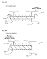
- Figs. 1A and 1B show cross-sectional schematic diagrams of the actuator in the present embodiment.
- Fig. 1A shows a voltage OFF state
- Fig. 1B shows a voltage ON state.
- an actuator 1 is provided with a dielectric film 10, electrodes 11a and 11b, and wirings 12a and 12b.
- the dielectric film 10 is made of H-NBR.
- the electrode 11a is disposed so as to cover approximately the entire upper surface of the dielectric film 10.
- the electrode 11b is disposed so as to cover approximately the entire lower surface of the dielectric film 10.
- the electrodes 11a and 11b are connected to a power source 13 by the wirings 12a and 12b, respectively.
- the electrodes 11a and 11b are both configured with the flexible conductive material of the present invention.
- the actuator 1 When switching from the OFF state to the ON state, voltage is applied between the pair of electrodes 11a and 11b. By applying voltage, the thickness of the dielectric film 10 decreases and, as shown by whited-out arrows in Fig. 1B , the dielectric film 10 proportionally extends horizontally with respect to the surfaces of the electrodes 11a and 11b. Thereby, the actuator 1 outputs a drive force in an up-down direction and a left-right direction in the drawing.
- the electrodes 11a and 11b are flexible, extendable, and contractible. Therefore, the electrodes 11a and 11b can be extended and contracted to follow deformation of the dielectric film 10. Specifically, the movement of the dielectric film 10 is less likely to be impeded by the electrodes 11a and 11b.
- ionized impurities are unlikely to be transferred from the electrodes 11a and 11b to the dielectric film 10. Therefore, electrical resistance of the dielectric film 10 is unlikely to be reduced. That is, when voltage is applied, electric current is unlikely to flow through the dielectric film 10. Accordingly, by applying voltage, a large number of electrical charges can be stored at the interface between the dielectric film 10 and the electrodes 11a and 11b.
- the actuator 1 has excellent durability.
- a larger voltage can be applied with the actuator 1. As a result, greater power can be generated.
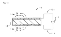
- Fig. 11 is a cross-sectional schematic view of an actuator in this embodiment (in a voltage OFF state). In Fig. 11 , components corresponding to Fig. 1A are shown with the same reference numerals.
- the actuator 1 is provided with the dielectric film 10, electrodes 14a and 14b, and the wirings 12a and 12b.
- the electrode 14a is disposed on an upper surface of the dielectric film 10.
- the electrode 14b is disposed on the lower surface of the dielectric film 10 so as to oppose the electrodes 14a with the dielectric film 10 sandwiched therebetween.
- the electrode 14a includes an inner conductive layer 140a and an outer conductive layer 141a.
- the inner conductive layer 140a is disposed so as to cover approximately the entire upper surface of the dielectric film 10.
- the inner conductive layer 140a is formed from the flexible conductive material of the present invention containing an adsorbent.
- the outer conductive layer 141 a is laminated on an upper surface of the inner conductive layer 140a.
- the outer conductive layer 141 a is formed from a flexible conductive material which includes silver powder in an elastomer (an easily ionizable additive such as a vulcanization accelerator is included as needed, but an adsorbent is not included).
- the outer conductive layer 141a is connected to the wiring 12a.
- the wiring 12a is connected to the power source 13.
- the electrode 14b includes an inner conductive layer 140b and an outer conductive layer 141b.
- the inner conductive layer 140b is disposed so as to cover approximately the entire lower surface of the dielectric film 10.
- the inner conductive layer 140b is formed with the flexible conductive material of the present invention containing an adsorbent.
- the outer conductive film 141b is laminated on a lower surface of the inner conductive layer 140b.
- the outer conductive layer 141b is formed with a flexible conductive material which includes silver powder with an elastomer (an easily ionizable additive such as a vulcanization accelerator is included as needed, but an adsorbent is not included).
- the outer conductive layer 141b is connected to the wiring 12b.
- the wiring 12b is connected to the power source 13.
- the inner conductive layers 140a and 140b which are in contact with the dielectric film 10 are both configured with the flexible conductive material of the present invention. Therefore, ionized impurities are unlikely to transfer from the electrodes 14a and 14b to the dielectric film 10.
- a capacitance-type sensor As a second example of the transducer of the present invention, an embodiment of a capacitance-type sensor is described. First, the configuration of the capacitance-type sensor of the present embodiment is described.
- Fig. 2 is a top view of the capacitance-type sensor.
- Fig. 3 is a cross-sectional view along a line III - III in Fig. 2 .
- a capacitance-type sensor 2 is provided with a dielectric film 20, a pair of electrodes 21a and 21b, wirings 22a and 22b, and cover films 23a and 23b.
- the dielectric film 20 is made of H-NBR and has a belt shape extending in a left-right direction.
- the thickness of the dielectric film 20 is approximately 300 ⁇ m.
- the electrode 21a has a rectangular shape. Three electrodes 21a are formed by screen printing on an upper surface of the dielectric film 20. Similarly, the electrode 21b has a rectangular shape. Three electrodes 21b are formed on a lower surface of the dielectric film 20 so as to oppose the electrodes 21 a with the dielectric film 20 sandwiched therebetween. The electrodes 21b are screen printed on the lower surface of the dielectric film 20. In this way, three pairs of the electrodes 21a and 21b are disposed with the dielectric film 20 sandwiched therebetween. The electrodes 21a and 21b are configured with the flexible conductive material of the present invention.
- the wiring 22a is individually connected to each of the electrodes 21 a formed on the upper surface of the dielectric film 20.
- the electrodes 21 a and a connector 24 are connected by the wiring 22a.
- the wiring 22a is formed by screen printing on the upper surface of the dielectric film 20.
- the wiring 22b is individually connected (shown by a dotted line in Fig. 2 ) to each of the electrodes 21b formed on the lower surface of the dielectric film 20.
- the electrodes 21b and a connector (not shown) are connected by the wiring 22b.
- the wiring 22b is formed by screen printing on the lower surface of the dielectric film 20.
- the wirings 22a and 22b are configured with the flexible conductive material of the present invention.
- the cover film 23a is made of acrylic rubber and has a belt shape extending in the left-right direction.
- the cover film 23a covers an upper surface of the dielectric film 20, the electrodes 21 a, and the wiring 22a.
- the cover film 23b is made of acrylic rubber and has a belt shape extending in the left-right direction.
- the cover film 23b covers the lower surface of the dielectric film 20, the electrodes 21b, and the wiring 22b.
- the capacitance-type sensor 2 moves downward as a single body. Due to compression, the thickness of the dielectric film 20 decreases. As a result, the capacitance between the electrodes 21a and 21b increases. Due to this capacitance change, deformation due to compression is detected.
- the dielectric film 20, the electrodes 21 a and 21b, the wirings 22a and 22b, and the cover films 23a and 23b are all configured with an elastomer material. Therefore, the entire capacitance-type sensor 2 is flexible, extendable, and contractible. In addition, the electrodes 21a and 21b and the wirings 22a and 22b can deform to follow deformation of the dielectric film 20.
- ionized impurities are unlikely to transfer from the electrodes 21a and 21b and from the wirings 22a and 22b to the dielectric film 20. Therefore, electrical resistance of the dielectric film 20 is unlikely to be reduced. Electric current is unlikely to flow through the dielectric film 20, and thus the possibility is small that detection accuracy will be reduced. In addition, electric current is unlikely to flow through the dielectric film 20, thus inhibiting the production of Joule heating. Accordingly, the possibility is small that the physical properties of the dielectric film 20 will change or that the dielectric film 20 will break due to the heat. In this way, the capacitance-type sensor 2 has excellent durability.
- the capacitance-type sensor 2 of the present embodiment is formed with three pairs of electrodes 21 a and 21 b opposing one another with the dielectric film 20 therebetween.
- the number, size, placement, and so on of the electrodes may be appropriately determined according to an intended use of the capacitance-type sensor 2.
- Figs. 4A and 4B are cross-sectional schematic diagrams of the power generating element in the present embodiment.
- Fig. 4A shows the power generating element during extension and
- Fig. 4B shows the power generating element during contraction.
- a power generating element 3 is provided with a dielectric film 30, electrodes 31a and 31b, and wirings 32a to 32c.
- the dielectric film 30 is made of H-NBR.
- the electrode 3 1 a is disposed so as to cover approximately an entire upper surface of the dielectric film 30.
- the electrode 31b is disposed so as to cover approximately an entire lower surface of the dielectric film 30.
- the electrode 31a is connected to the wirings 32a and 32b. Specifically, the electrode 31a is connected to an external load (not pictured) via the wiring 32a. Also, the electrode 31 a is connected to a power source (not pictured) via the wiring 32b.
- the electrode 31b is grounded by the wiring 32c.
- the electrodes 31a and 31b are both configured with the flexible conductive material of the present invention.
- the thickness of the dielectric film 30 decreases and electrical charge can be stored between the electrodes 31a and 31b. Thereafter, when the compressive force is removed, as shown in Fig. 4B , the dielectric film 30 contracts due to an elastic restorative force thereof and the film thickness increases. Thereupon, the stored electrical charge is released through the wiring 32a.
- the electrodes 31a and 31b are flexible, extendable, and contractible. Therefore, the electrodes 31a and 31b can be extended and contracted to follow deformation of the dielectric film 30. Specifically, movement of the dielectric film 30 is unlikely to be impeded by the electrodes 31a and 31b.
- ionized impurities are unlikely to transfer from the electrodes 31a and 31b to the dielectric film 30. Therefore, the electrical resistance of the dielectric film 30 is unlikely to be reduced. That is, during compression, electric current is unlikely to flow through the dielectric film 30.
- the power generating element 3 has excellent durability.
- Fig. 5 is a perspective view of the speaker of the present embodiment.
- Fig. 6 is a cross-sectional view along a line VI - VI in Fig. 5 . As shown in Figs.
- a speaker 4 is provided with a first outer frame 40a, a first inner frame 41a, a first dielectric film 42a, a first outer electrode 43 a, a first inner electrode 44a, a first vibration plate 45a, a second outer frame 40b, a second inner frame 41b, a second dielectric film 42b, a second outer electrode 43b, a second inner electrode 44b, a second vibration plate 45b, eight bolts 460, eight nuts 461, and eight spacers 462.
- the first outer frame 40a and first inner frame 41a are each made of resin and have a ring shape.
- the first dielectric film 42a is made of H-NBR and has a circular thin film shape.
- the first dielectric film 42a is spread out between the first outer frame 40a and the first inner frame 41 a. Specifically, the first dielectric film 42a is held between and fixed in place by the first outer frame 40a on a front side and the first inner frame 41 a on a back side, in a state ensuring a predetermined tensile force.
- the first vibration plate 45a is made of resin and has a round plate shape.
- the first vibration plate 45a has a diameter smaller than the first dielectric film 42a.
- the first vibration plate 45a is disposed in the approximate center of a front surface of the first dielectric film 42a.
- the first outer electrode 43a has a ring shape.
- the first outer electrode 43a is glued to a front surface of the first dielectric film 42a.
- the first inner electrode 44a also has a ring shape.
- the first inner electrode 44a is glued to a back surface of the first dielectric film 42a.
- the first outer electrode 43a and the first inner electrode 44a are reversed in a front-back direction to one another with the first dielectric film 42a sandwiched therebetween.
- the first outer electrode 43a and the first inner electrode 44a are both configured with the flexible conductive material of the present invention.
- the first outer electrode 43a is provided with a terminal 430a.
- the first inner electrode 44a is provided with a terminal 440a. Voltage is applied to the terminals 430a and 440a from the exterior.
- the configuration, materials, and shapes of the second outer frame 40b, the second inner frame 41b, the second dielectric film 42b, the second outer electrode 43b, the second inner electrode 44b, and the second vibration plate 45b are similar to the configuration, materials, and shapes of the first outer frame 40a, the first inner frame 41a, the first dielectric film 42a, the first outer electrode 43a, the first inner electrode 44a, and the first vibration plate 45a (hereafter, abbreviated as "the primary components”).
- the placement of the secondary components is symmetrical in the front-back direction with the placement of the primary components described above.
- the second dielectric film 42b is made of H-NBR and is spread out between the second outer frame 40b and the second inner frame 41b.
- the second vibration plate 45b is disposed in the approximate center of the front surface of the second dielectric film 42b.
- the second outer electrode 43b is printed on a front surface of the second dielectric film 42b.
- the second inner electrode 44b is printed on a back surface of the second dielectric film 42b.
- the second outer electrode 43b and the second inner electrode 44b are both configured with the flexible conductive material of the present invention. Voltage is applied to a terminal 430b of the second outer electrode 43b and a terminal 440b of the second inner electrode 44b from the exterior.
- the primary and secondary components are fixed in place by the eight bolts 460 and the eight nuts 461 via the eight spacers 462.
- the set of "bolt 460-nut 461-spacer 462" is disposed in a circumferential direction of the speaker 4 separated by predetermined intervals.
- the bolts 460 penetrate from the front surface of the first outer frame 40a to the front surface of the second outer frame 40b.
- the nuts 461 screw onto a through-end of the bolts 460.
- the spacers 462 are made of resin and encircle a shaft of the bolts 460.
- the spacers 462 ensure a predetermined gap between the first inner frame 41a and the second inner frame 41b.
- a back surface of a central portion of the first dielectric film 42a (back side of a portion where the first vibration plate 45a is disposed) and a back surface of a central portion of the second dielectric film 42b (back side of a portion where the second vibration plate 45b is disposed) are joined. Therefore, in a direction shown in Fig. 6 by a whited-out arrow Y1a, a biasing force builds up on the first dielectric film 42a. Also, in a direction shown in Fig. 6 by a whited-out arrow Y1b, a biasing force builds up on the second dielectric film 42b.
- a predetermined voltage (offset voltage) is applied via the terminals 430a and 440a and the terminals 430b and 440b to the first outer electrode 43a and the first inner electrode 44a and to the second outer electrode 43b and the second inner electrode 44b.
- voltage of the opposite phase is applied to the terminals 430a and 440a and to the terminals 430b and 440b.
- an offset voltage +1 V is applied to the terminals 430a and 440a, the film thickness within the first dielectric film 42a decreases for a portion disposed between the first outer electrode 43a and the first inner electrode 44a.
- the portion extends in a radial direction. Concurrently therewith, voltage of the opposite phase (offset voltage -1 V) is applied to the terminals 430b and 440b. The film thickness then increases for a portion within the second dielectric film 42b disposed between the second outer electrode 43b and the second inner electrode 44b. In addition, the portion contracts in a radial direction.
- the second dielectric film 42b is elastically deformed by its own biasing force in the direction shown by the whited-out arrow Y1b in Fig. 6 .
- the first dielectric film 42a is elastically deformed by its own biasing force in the direction shown by the whited-out arrow Y1a in Fig. 6 . In this way, the air is vibrated by vibrating the first vibration plate 45a and the second vibration plate 45b to produce sound.
- the first outer electrode 43a, the first inner electrode 44a, the second outer electrode 43b, and the second inner electrode 44b are flexible, extendable, and contractible. Therefore, the first outer electrode 43a and the first inner electrode 44a can extend and contract to follow deformation of the first dielectric film 42a. Similarly, the second outer electrode 43b and the second inner electrode 44b can extend and contract to follow the deformation of the second dielectric film 42b. That is, movement of the first dielectric film 42a and the second dielectric film 42b are less likely to be impeded by the electrodes 43a, 44a, 43b, and 44b.
- ionized impurities are unlikely to transfer from the first outer electrode 43a and the first inner electrode 44a to the first dielectric film 42a.
- ionized impurities are unlikely to transfer from the second outer electrode 43b and the second inner electrode 44b to the second dielectric film 42b. Therefore, when voltage is applied, electric current is unlikely to flow through the first dielectric film 42a and the second dielectric film 42b. Accordingly, the possibility is small that physical properties of the first dielectric film 42a and the second dielectric film 42b will be changed and that the first dielectric film 42a and the second dielectric film 42b will break due to Joule heating. In this way, the speaker 4 has excellent durability.
- the flexible wiring board of the present invention is provided with an elastic base material and a wiring disposed on a front surface of the elastic base material.
- the material of the elastic base material is not particularly limited. Examples include, as materials having extendibility and contractibility, silicone rubber, ethylene-propylene copolymer rubber, natural rubber, styrene-butadiene copolymer rubber, acrylonitrile-butadiene rubber (NBR), acrylic rubber, epichlorohydrin rubber, chlorosulfonate polyethylene, chlorinated polyethylene, urethane rubber, fluorine rubber, chloroprene rubber, isobutylene isoprene rubber, and various kinds of thermoplastic elastomers.
- the wiring is configured with the flexible conductive material of the present invention.
- the configuration of the flexible conductive material of the present invention and the manufacturing method thereof are as described above. Accordingly, their description is omitted here.
- the flexible wiring board of the present invention also, employing a favorable embodiment of the flexible conductive material of the present invention described above is preferred.
- the wiring may be formed with two or more conductive layers of different materials. In such a case, the conductive layer in contact with the elastic base material is preferably formed with the flexible conductive material of the present invention.
- an embodiment of the flexible wiring board of the present invention is described.
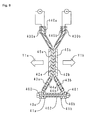
- Fig. 7 is a transparent top view of a flexible wiring board of the present embodiment. Moreover, in Fig. 7 , electrodes and wirings on a back side are illustrated with thin lines. As shown in Fig. 7 , a flexible wiring board 6 is provided with an elastic base material 60, front electrodes 01X - 16X, back electrodes 01Y - 16Y, front wirings 01x - 16x, back wirings 01y - 16y, a front wiring connector 61, and a back wiring connector 62.
- the elastic base material 60 is made of urethane rubber and has a sheet shape.
- a total of sixteen front electrodes 01X - 16X are disposed on an upper surface of the elastic base material 60.
- the front electrodes 01X - 16X each have a belt shape.
- the front electrodes 01X-16X each extend in an X direction (left-right direction).
- the front electrodes 01X - 16X are disposed so as to be spaced at a predetermined interval in a Y direction (front-back direction) and so as to be approximately parallel to one another.
- a total of sixteen back electrodes 01Y - 16Y are disposed on a lower surface of the elastic base material 60.
- the back electrodes 01Y - 16Y each have a belt shape.
- the back electrodes 01Y - 16Y each extend in the Y direction.
- the back electrodes 01Y - 16Y are disposed so as to be spaced at a predetermined interval in the X direction and so as to be approximately parallel to one another.
- portions where the front electrodes 01X - 16X and the back electrodes 01Y - 16Y intersect with one another having the elastic base material 60 therebetween (overlapping portions) form detectors where a load and the like is detected.
- a total of sixteen front wirings 01x - 16x are disposed on the upper surface of the elastic base material 60.
- the front wirings 01x - 16x each have a line shape.
- the front wirings 01x - 16x are configured with the flexible conductive material of the present invention.
- the front wiring connector 61 is disposed in a left back corner of the elastic base material 60.
- the front wirings 01x - 16x are each connected to the left ends of the front electrodes 01X - 16X and to the front wiring connector 61.
- the upper surface of the elastic base material 60, the front electrodes 01X - 16X, and the front wirings 01x - 16x are covered from above by a front cover film (not shown).
- a total of sixteen back wirings 01y - 16y are disposed on the lower surface of the elastic base material 60.
- Each of the back wirings 01y - 16y has a line shape.
- the back wirings 01y - 16y are configured with the flexible conductive material of the present invention.
- the back wiring connector 62 is disposed in a left front corner of the elastic base material 60.
- the back wirings 01y-16y each connect a front end of the back electrodes 01Y - 16Y and the back wiring connector 62.
- the lower surface of the elastic base material 60, the back electrodes 01Y - 16Y, and the back wirings 01y - 16y are covered from below by a back cover film (not shown).
- the front wiring connector 61 and the back wiring connector 62 are each electrically connected to an arithmetic portion (not shown). Impedance in the detector is input from the front wirings 01x - 16x and the back wirings 01y - 16y into the arithmetic portion. Based on this, surface pressure distribution is measured.
- the front wirings 01x - 16x and the back wirings 01y - 16y are each flexible, extendable, and contractible. Therefore, the front wirings 01x - 16x and the back wirings 01y - 16y can deform to follow the deformation of the elastic base material 60. Also, according to the present embodiment, ionized impurities are unlikely to transfer from the front wirings 01x - 16x and the back wirings 01y - 16y to the elastic base material 60. Therefore, the possibility is small that the electrical resistance of the elastic base material 60 will be reduced and that electric current will flow into the elastic base material 60. Accordingly, malfunctions are inhibited. Further, because electric current is unlikely to flow into the elastic base material 60, the possibility is small that the elastic base material 60 will break due to Joule heating. Therefore, the flexible wiring board 6 has excellent durability.
- the electromagnetic shield of the present invention is configured with the flexible conductive material of the present invention.
- the electromagnetic shield fulfills a role inhibiting electromagnetic waves generated within an electronic device from leaking to the exterior, and making it unlikely that electromagnetic waves from the exterior will intrude to the interior thereof.
- a coating material of the flexible conductive material of the present invention formed by dissolving a raw material such as rubber polymer in a predetermined solvent may be coated on the inner circumferential surface of the case for the electronic device and may then be cross-linked.
- the electromagnetic shield can be disposed in the capacitance-type sensor shown as the second embodiment of the transducer described above.
- the electromagnetic shield may be disposed so as to coat each of a top surface of the cover film 23a and a bottom surface of the cover film 23b (see Figs. 2 and 3 , mentioned previously).
- the coating material for the flexible conductive material of the present invention may be coated on the top surface of the cover film 23a and the bottom surface of the cover film 23b and may then be cross-linked.
- the flexible conductive material of the present invention may be molded into a desired shape and then employed.
- the flexible conductive material of examples 1 - 8 was produced from the raw materials shown in Tables 1 and 2, below.
- an acrylic rubber polymer containing an epoxy group (“Nipol (registered trademark) AR42W” manufactured by Zeon Corporation), zinc dimethyldithiocarbamate (“Nocceler (registered trademark) PZ” manufactured by Ouchi Shinko Chemical Industrial) as a vulcanization accelerator, and ferric dimethyldithiocarbamate (“Nocceler TTFE” manufactured by Ouchi Shinko Chemical Industrial) were mixed by a roll kneader.
- the obtained mixture was dissolved in methyl ethyl ketone (MEK).
- a conductive agent ("Ketjen Black (registered trademark) EC-600JD" manufactured by Lion Corporation) was added to the MEK solution and agitated by a dyno mill. Then, a predetermined adsorbent was added to the agitated MEK solution and was processed for five minutes in an ultrasonic homogenizer. A rubber composition was prepared thereby. Next, the prepared rubber composition was coated on a base material with a bar coating method to form a coating film with a thickness of approximately 20 ⁇ m. Then, after being dried, the coating film was heated for 30 minutes at 170° C to advance a cross-linking reaction. In this way, the flexible conductive material of examples 1 - 8 was produced.
- the flexible conductive material of example 9 was produced as described above except that the conductive agent was changed to silver powder ("FA-D-4" manufactured by DOWA Electronics Materials Co. Ltd.).
- the flexible conductive material of example 10 was produced by changing the elastomer to a thermoplastic urethane elastomer.
- the thermoplastic urethane elastomer ("Nippolan (registered trademark) 5193" manufactured by Nippon Polyurethane Industry Co. Ltd.) was dissolved in MEK.
- the conductive agent Kertjen Black (same as above)
- the adsorbent activate carbon
- the rubber composition was prepared thereby.
- the prepared rubber composition was coated on a base material with the bar coating method to form a coating film with a thickness of approximately 20 ⁇ m. Then, after being dried, the coating film was heated for 30 minutes at 150° C to harden. In this way, the flexible conductive material of example 10 was produced.
- the flexible conductive material of examples 12 and 13 was produced similarly to the flexible conductive material of examples 1 - 8 except that activated carbon or mesoporous carbon having conductivity was included as an adsorbent and the conductive agent Ketjen Black was not included.
- the activated carbon or mesoporous carbon added as an adsorbent fulfilled the role of the conductive agent.
- the flexible conductive material of example 14 was produced similarly to example 9 described above, except that the included amount of silver powder in the conductive agent was changed and a vulcanization accelerator was not included.
- the flexible conductive material of comparative example 1 was produced similarly to the flexible conductive material of examples 1 - 8, except that an adsorbent was not included.
- the flexible conductive material of comparative example 2 was produced similarly to the flexible conductive material of example 9, except that an adsorbent was not included.
- the flexible conductive material of comparative example 3 was produced similarly to the flexible conductive material of example 14, except that an adsorbent was not included.
- the rubber composition prior to cross-linking in the manufacturing process of the flexible conductive material of example 7 was coated onto a base material by the bar coating method to form a coating film having a thickness of approximately 20 ⁇ m.
- the rubber composition prior to cross-linking in the manufacturing process of the flexible conductive material of comparative example 2 was coated onto a top surface of the formed coating film with the bar coating method to form a coating film having a thickness of approximately 20 ⁇ m.
- the two laminated layers of coating film were vulcanization-bonded. In this way, a conductive laminate body of example 11 was produced.
- Tables 1 and 2 show the type and included amount of raw materials used.
- a fumed silica "Aerosil (registered trademark) 380" manufactured by Nippon Aerosil Co. Ltd. (pH 3.7 - 4.7, specific surface area 380 m 2 /g) was used as a silica.
- "Dowex (registered trademark) 50Wx8 200-400” manufactured by Dow Chemical Company was used as an H positive ion-exchange resin.
- "YP-50F” manufactured by Kuraray Chemical Co. Ltd. was used as an activated carbon.
- the degree of advancement in cross-linking was measured. First, 1 g of a test sample prepared from each flexible conductive material was immersed in 30 g of MEK. After dormancy therein for 4 hours at room temperature, the test sample was extracted and dried. Then, the mass of the test sample after drying was measured and a ratio of dried mass to initial mass (MEK insoluble) was calculated.
- an elastic modulus was calculated from stress-extension curves in a tensile test according to JIS K7127 (1999).
- the shape of the test sample was a Type 2 test sample.
- the tensile stress (M25) during 25% extension of the above flexible conductive materials and conductive laminate body was measured according to JIS K 6251 (2004).
- the shape of the test sample was Dumbbell No. 5-shaped.
- volume resistivity was measured according to a parallel terminal electrode method in JIS K6271 (2008).
- a commercially available butyl rubber sheet manufactured by Tigers Polymer Corporation was used as an insulating resin support tool supporting the flexible conductive material and the like (test sample).
- a dielectric film for an adherend was prepared as follows. First, a hydrogenated nitrile rubber containing a carboxyl group ("Therban (registered trademark) XT8889" manufactured by Lanxess AG) was dissolved in acetyl acetone. Next, tetrakis(2-ethylhexyloxy)titanium was added to the solution and mixed. Then, the obtained mixed solution was coated on a base material with the bar coating method and dried to form a coating film with a thickness of 18 ⁇ m. The coating film was cut in a rectangular shape of 50 mm in length and 25 mm in width to make a pre-cross-linking dielectric film.
- Therban registered trademark
- XT8889 manufactured by Lanxess AG
- the coating film of the rubber composition prior to cross-linking was cut in a rectangular shape of 38 mm in length and 20 mm in width to make a pre-cross-linking electrode. Then, one pre-cross-linking electrode was disposed on each of the front and back surfaces of the pre-cross-linking dielectric film. Then, by heating for 30 minutes at 170° C, the dielectric film and the electrodes were vulcanization-bonded. In this way, a first element for testing was produced.
- the two layers of coating film in the manufacturing process of the conductive laminate body of example 11 were cut in a rectangular shape of 38 mm in length and 20 mm in width to make a pre-cross-linking electrode. Then, one pre-cross-linking electrode was disposed on each of the front and back surfaces of the pre-cross-linking dielectric film. Then, by heating for 30 minutes at 170° C, the dielectric film and the electrodes were vulcanization-bonded. The pre-cross-linking electrodes were each disposed such that the coating film of example 7 was in contact with the pre-cross-linking dielectric film. In this way, a second element for testing was produced.
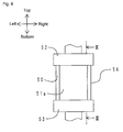
- Fig. 8 is a front view of an obverse side of the first element for testing mounted in the testing device.
- Fig. 9 is a cross-sectional view along a line IX - IX in Fig. 8 .
- a top edge of a first element for testing 5A was gripped by an upper chuck 52 in the testing device.
- a bottom edge of the first element for testing 5A was gripped by a lower chuck 53.
- the first element for testing 5A, the upper chuck 52, and the lower chuck 53 were each insulated.
- the first element for testing 5A was mounted between the upper chuck 52 and the lower chuck 53 in a state pre-extended in an up-down direction (extension ratio of 25%).
- the first element for testing 5A was configured with a dielectric film 50 and a pair of electrodes 51a and 51b.
- the electrodes 51a and 51b were disposed opposite one another in a front-back direction with the dielectric film 50 sandwiched therebetween.
- the electrodes 51a and 51b were disposed in a state offset by 8 mm in the up-down direction. That is, the electrodes 51a and 51b overlapped across the dielectric film 50 within a range of 30 mm in length and 20 mm in width.
- a wiring (not shown) was connected to a bottom end of the electrode 51a.
- a wiring (not shown) was connected to a top end of the electrode 51b.
- the electrodes 51a and 51b were connected to a power source (not shown) via their respective wirings.
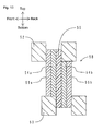
- FIG. 10 is a cross-sectional view of the second element for testing mounted in the testing device.
- Fig. 10 corresponds to Fig. 9 . Accordingly, components in Fig. 10 which correspond to those in Fig. 9 are shown with the same reference numbers.
- a top end of a second element for testing 5B was gripped by the upper chuck 52 in the testing device.
- a bottom end of the second element for testing 5B was gripped by the lower chuck 53.
- the second element for testing 5B, the upper chuck 52, and the lower chuck 53 were each insulated.
- the second element for testing 5B was mounted between the upper chuck 52 and the lower chuck 53 in a state pre-extended in the up-down direction (extension ratio of 25%).
- the second element for testing 5B was configured with the dielectric film 50, a pair of inner electrodes 54a and 54b, and a pair of outer electrodes 55a and 55b.
- the inner electrodes 54a and 54b were configured with the flexible conductive material of example 7.
- the inner electrodes 54a and 54b were disposed opposite one another in a front-back direction with the dielectric film 50 sandwiched therebetween.
- the inner electrodes 54a and 54b were disposed in a state offset by 8 mm in the up-down direction. That is, the inner electrodes 54a and 54b overlapped across the dielectric film 50 in a range of 30 mm in length and 20 mm in width.
- the outer electrodes 55a and 55b were configured with the flexible conductive material of comparative example 2.
- the outer electrode 55a was laminated on a front surface of the inner electrode 54a.
- the outer electrode 55b was laminated on a back surface of the inner electrode 55b.
- a bottom end of the outer electrode 55a was connected to a wiring (not shown).
- a top end of the outer electrode 55b was connected to a wiring (not shown).
- the outer electrodes 55a and 55b were connected to a power source (not shown) via their respective wirings. Direct current voltage having an electric field strength of 10, 20, or 30 V/ ⁇ m was applied in order to the outer electrodes 55a and 55b, then the value of electric current flowing between the outer electrodes 55a and 55b was measured.
- the first element for testing 5A and the second element for testing 5B were left dormant for one month in an environment of 40° C in temperature and 95% humidity. Thereafter, with each of the measurement methods described above, direct current voltage having an electric field strength of 20 V/ ⁇ m was applied and the value of electric current flowing between the electrodes was measured.
- the results of the evaluation are collectively shown in Tables 1 and 2 above.
- the MEK insoluble in the flexible conductive material of example 3 in which trimercaptotriazine (TMT) has been included has a value near 100%.
- TMT trimercaptotriazine
- this value is considerably larger. In this way, in the flexible conductive material of example 3 in which TMT has been included, an improvement in cross-linking density has been confirmed.
- an elastic modulus becomes larger in accordance with an increase in the included amount of an adsorbent and a conductive agent.
- the flexible conductive material of examples 1, 2, 4, 5, 7, 8, 10, 12, and 13 show high conductivity to a similar degree to the flexible conductive material of comparative example 1
- the flexible conductive material of examples 9 and 14 and the conductive laminate body of example 11 show high conductivity to a similar degree to the flexible conductive material of comparative example 2.
- leakage current is small when the flexible conductive material of the examples is made into an electrode.
- leakage current is small when the flexible conductive material of examples 7 - 10, 12, and 13, which used activated carbon or mesoporous carbon as an adsorbent, is made into an electrode.
- leakage current is also small in a case where the conductive laminate body of example 11, in which the flexible conductive material of example 7 and the flexible conductive material of comparative example 2 are laminated, is made into an electrode. Also, in a case where the elements for testing were left dormant for a month in a high humidity environment, leakage current did not change much in all of the examples.
- An adsorbent is included in the flexible conductive material of the examples. Therefore, impurity ions such as reaction residue left within an elastomer and silver ions in which silver of the conductive agent has ionized are adsorbed and fixed in the adsorbent. Accordingly, the impurities transferring from the flexible conductive material (electrode) to the dielectric film are reduced and a reduction in electrical resistance of the dielectric film may be inhibited.
- leakage current becomes smaller accompanying an increase in an included amount of silica. This may be considered to be due to an adsorbed amount of impurity ions increasing when the content amount of silica becomes greater, and additionally due to the impurity ions themselves becoming unlikely to transfer.
- the flexible conductive material of the present invention is favorable as a material for electrodes and wiring of a flexible transducer using an elastomer.
- the flexible conductive material of the present invention is also favorable as a wiring material for a flexible wiring board used in control of movable components for robots and industrial machinery, in wearable devices, in bendable displays, and the like.
- the flexible conductive material of the present invention is also favorable as an electromagnetic shield.
Landscapes
- Chemical & Material Sciences (AREA)
- Dispersion Chemistry (AREA)
- Spectroscopy & Molecular Physics (AREA)
- Physics & Mathematics (AREA)
- Health & Medical Sciences (AREA)
- Chemical Kinetics & Catalysis (AREA)
- Medicinal Chemistry (AREA)
- Polymers & Plastics (AREA)
- Organic Chemistry (AREA)
- Microelectronics & Electronic Packaging (AREA)
- Engineering & Computer Science (AREA)
- Compositions Of Macromolecular Compounds (AREA)
- Conductive Materials (AREA)
- Parts Printed On Printed Circuit Boards (AREA)
- Shielding Devices Or Components To Electric Or Magnetic Fields (AREA)
Abstract

Description
- The present invention relates to a flexible conductive material which is favorable for an extendable and contractible electrode, a wiring, and the like, and to a transducer, a flexible wiring board, and an electromagnetic shield using the same.
- Using a polymer material such as a dielectric elastomer, development has advanced for small, light-weight transducers having a high degree of flexibility. Examples of a transducer include an actuator in which a pair of electrodes is disposed on both a front and back surface of a dielectric film made from an elastomer (see, for example,
Patent Documents 1 and 2). In an actuator of this type, when the applied voltage between the electrodes is increased, an electrostatic attraction between the electrodes increases. Therefore, the dielectric film sandwiched between the electrodes is compressed in a thickness direction and the thickness of the dielectric film decreases. When the film thickness decreases, the dielectric film proportionally extends in a horizontal direction with respect to the electrode surfaces. Meanwhile, when the applied voltage between the electrodes is reduced, the electrostatic attraction between the electrodes decreases. Therefore, the compressive force on the dielectric film in the thickness direction is reduced, and the film thickness increases due to an elastic restorative force of the dielectric film. When the film thickness increases, the dielectric film proportionally contracts in the horizontal direction with respect to the electrode surfaces. In this way, the actuator drives drive target members by extension and contraction of the dielectric film in response to the magnitude of the applied voltage. - In the actuator, the electrodes are affixed to both the front and back surfaces of the dielectric film. Accordingly, the electrodes must be extendable and contractible in response to deformation of the dielectric film so as not to interfere with the extension and contraction thereof.
-
- Patent Document 1: Japanese Patent Publication No.
2003-506858 - Patent Document 2: Japanese Patent Laid-open Publication No.
2009-296703 - The extendable and contractible electrodes can, for example and as disclosed in
Patent Document 2, be formed from a flexible conductive material in which a conductive agent such as carbon black is included in an elastomer. However, when an elastomer is used, impurities in the elastomer are a negative feature. For example, in the case of sulfur cross-linking, unreacted sulfur, vulcanization accelerators, and the like as well as products (reaction residue) of sulfur, vulcanization accelerators, and the like commonly remain in the elastomer after cross-linking. Further, even a rubber polymer raw material contains reaction residues such as initiators, emulsifiers, and chain transfer agents added during a polymerization reaction. These reaction residues are impurities in the elastomer. Accordingly, when an electrode is formed on a surface of a dielectric film from a flexible conductive material containing the elastomer described above, there is a possibility that impurities in the electrode (flexible conductive material) may ionize and transfer to the dielectric film. Further, in a case where a metallic powder (e.g., silver powder) is used as the conductive agent, there is a possibility that ionized silver (Ag+) may transfer to the dielectric film and be deposited as silver (migration). - There is a further possibility that impurities contained in a member (such as a dielectric film) touching the flexible conductive material may, after transferring to the flexible conductive material, transfer once more to the member. These impurities may be, for example, zinc salt and iron salt of dimethyldithiocarbamate used as a cross-linking promoter; sodium salt and zinc salt of 2-mercaptobenzothiazole; hydrolysate of an organic phosphate compound of tricresylphosphate and the like used as a plasticizer and fire retardant; quaternary ammonium salt derived from a surfactant; and various other metallic ions (Na+, K+, Mg2+) contained in trace amounts. Thus, the influence of impurities contained in the member touching the flexible conductive material cannot be ignored.
- According to investigations by the inventors of the present invention, it was verified that when a pre-cross-linking flexible conductive material is coated on a dielectric film, also prior to cross-linking, and the flexible conductive material and the dielectric film are integrally cross-linked, impurities from the flexible conductive material are more likely to transfer to the dielectric film.
- When the ionized impurities transfer through the dielectric film, electrical resistance of the dielectric film is reduced. Therefore, when voltage is applied, electric current flows through the dielectric film more easily (so-called leakage current increases). Accordingly, electric charge is unlikely to be stored at an interface between the dielectric film and the electrode, and power consumption increases. Further, when electric current flows through the dielectric film, Joule heating is produced. There is a possibility that physical properties of the dielectric film may be changed by the heat produced. Moreover, the dielectric film is more likely to break. That is, resistance of the dielectric film to electric breakdown is reduced. When the resistance of the dielectric film to electric breakdown is reduced, a large voltage cannot be applied to the actuator, for example. Accordingly, adequate power and displacement amount cannot be obtained.
- Besides actuators, the transfer of impurities is also a negative feature in sensors, power generating elements, and the like in which electrodes are disposed with a dielectric film therebetween. Further, the transfer of impurities also becomes a negative feature in a case where wiring and the like is formed on a surface of an elastic base material such as an elastomer, the wiring and the like being formed from a flexible conductive material containing an elastomer. Specifically, due to the transfer of impurities from the flexible conductive material to the elastic base material, there is a possibility that electrical resistance of the elastic base material may be reduced and leakage current may occur.
- The present invention is conceived in light of such conditions, and has as its purpose to provide a flexible conductive material in which the transfer of impurities to an adherend such as a dielectric film is reduced. Further, the present invention has as its purpose to provide a transducer and a flexible wiring board having a small leakage current and excellent durability by forming an electrode and a wiring from the flexible conductive material. Further, the present invention has as its purpose to provide an electromagnetic shield having a small leakage current using the flexible conductive material.
- (1) To resolve the above problem, a flexible conductive material of the present invention includes an elastomer, a conductive agent filled in the elastomer, and an adsorbent fixed inside the elastomer and able to adsorb ionic material.
- The adsorbent is incorporated into the flexible conductive material of the present invention. The adsorbent is able to adsorb ionic material. Specifically, the adsorbent can adsorb impurities that have ionized within the elastomer. Further, the adsorbent is fixed inside the elastomer. Therefore, the impurities adsorbed to the adsorbent stay inside the elastomer and do not transfer from the elastomer to the exterior (to another member touching the flexible conductive material). Herein, the adsorbent preferably does not transfer from inside the cross-linked structure (polymer network) of the elastomer to the exterior. Therefore, the adsorbent and the elastomer may be either chemically bonded or not.
- In this way, according to the flexible conductive material of the present invention, ionized impurities are unlikely to transfer to another member touching the flexible conductive material. Further, even when an ionized impurity is transferred thereto from the other members touching the flexible conductive material of the present invention, the impurity can be inhibited from transferring once more to the other members. Therefore, in a case where an electrode is formed from the flexible conductive material of the present invention to configure a transducer for an actuator or the like, few impurities transfer from the electrode to the dielectric film. Thus, electrical resistance of the dielectric film is unlikely to be reduced. That is, during application of voltage, electric current is unlikely to flow through the dielectric film. Accordingly, power consumption can be reduced and many electric charges can be stored at an interface between the dielectric film and the electrode. Further, electric current is unlikely to flow through the dielectric film and therefore the production of Joule heating is inhibited. Therefore, the possibility is low that physical properties of the dielectric film will change or that the dielectric film will break due to heat. In this way, according to the flexible conductive material of the present invention, it is possible to achieve an electrode and a wiring in which deformation of the dielectric film is unlikely to be restricted and few impurities transfer to the dielectric film.
- (2) A transducer of the present invention includes a dielectric film made of an elastomer, a plurality of electrodes disposed with the dielectric film therebetween, and a wiring connecting each of the plurality of electrodes. At least one of the electrodes and the wiring is configured with the flexible conductive material of the present invention.
- The transducer is an apparatus converting energy of a certain type into energy of another type. The transducer contains an actuator, a sensor, a power generating element, and the like converting mechanical energy into electrical energy; alternatively, the transducer contains a speaker, a microphone, and the like converting acoustic energy into electrical energy.
- According to the transducer of the present invention, at least one of the electrodes and the wiring (referred to "electrodes and the like" hereafter, where appropriate) is formed from the flexible conductive material of the present invention described above. Accordingly, when the dielectric film deforms, the electrodes and the like extend and contract to follow the deformation. Therefore, the movement of the dielectric film is unlikely to be impeded. Further, few impurities transfer from the electrodes and the like to the dielectric film. Therefore, the possibility is low that the electrical resistance of the dielectric film will be reduced. Accordingly, during application of voltage, electric current is unlikely to flow through the dielectric film. That is, the possibility is low that the physical properties of the dielectric film will change or that the dielectric film will break due to heat. Accordingly, the transducer of the present invention has excellent durability. Further, when the transducer of the present invention is used as an actuator, a large voltage can be applied to the dielectric film. Accordingly, greater power can be generated by increasing the applied voltage.
- (3) A flexible wiring board of the present invention includes an elastic base material and a wiring disposed on a surface of the elastic base material. At least a portion of the wiring is configured with the flexible conductive material of the present invention described above.
- According to the flexible wiring board of the present invention, the wiring extends and contracts to follow deformation of the elastic base material. Accordingly, the flexible wiring board of the present invention is favorable as wiring for movable components and components having a complex shape. Further, few impurities transfer from the wiring to the elastic base material. Therefore, the possibility is low that the electrical resistance of the elastic base material will be reduced and that electric current will flow into the elastic base material. Therefore, a malfunction is inhibited. Further, the possibility is low that the physical properties of the elastic base material will change and that the elastic base material will break due to Joule heating. In this way, the flexible wiring board of the present invention has excellent durability.
- (4) An electromagnetic shield of the present invention is configured with the flexible conductive material of the present invention.
- The flexible conductive material of the present invention can be manufactured from a coating material in which a raw material such as a rubber polymer is dissolved in a predetermined solvent. Alternatively, the flexible conductive material of the present invention can be formed in various shapes from a kneaded raw material. Therefore, the flexible conductive material of the present invention is easily disposed as an electromagnetic shield in various positions where shielding from electromagnetic waves is desired. Further, according to the electromagnetic shield of the present invention, impurities in the electromagnetic shield (flexible conductive material) are unlikely to transfer to a member touching the electromagnetic shield. Therefore, the possibility is low that the electrical resistance of the touching member will be reduced, and that leakage current will occur. Accordingly, the possibility is low that the physical properties of the touching member will change and that the member will break due to Joule heating.
-
-
Figs. 1A and 1B are cross-sectional schematic diagrams of an actuator in a first embodiment of a transducer of the present invention,Fig. 1A showing a voltage OFF state andFig. 1B showing a voltage ON state; -
Fig. 2 is a top view of a capacitance-type sensor in a second embodiment of the transducer of the present invention; -
Fig. 3 is a cross-sectional view along a line III - III inFig. 2 ; -
Figs. 4A and 4B are cross-sectional schematic diagrams of a power generating element in a third embodiment of the transducer of the present invention,Fig. 4A showing the power generating element during extension andFig. 4B showing the power generating element during contraction. -
Fig. 5 is a perspective view of a speaker in a fourth embodiment of the transducer of the present invention; -
Fig. 6 is a cross-sectional view along a line VI - VI inFig. 5 ; -
Fig. 7 is a transparent top view of a flexible wiring board of the present invention; -
Fig. 8 is front view of an obverse side of a first element for testing mounted in a measurement device; -
Fig. 9 is a cross-sectional view along a line IX - IX inFig. 8 ; -
Fig. 10 is a cross-sectional view of a second element for testing mounted in a testing device; -
Fig. 11 is a cross-sectional schematic view of an actuator in a fifth embodiment of the transducer of the present invention. - 1: actuator (transducer); 10: dielectric film; 11a and 11b: electrode; 12a and 12b: wiring; 13: power source; 14a and 14b: electrode; 140a and 140b: inner conductive layer; 141a and 141b: outer conductive layer. 2: capacitance-type sensor (transducer); 20: dielectric film; 21a and 21b: electrode; 22a and 22b: wiring; 23a and 23b: cover film; 24: connector. 3: power generating element (transducer); 30: dielectric film; 31a and 31b: electrode; 32a - 32c: wiring. 4: speaker (transducer); 40a: first outer frame; 40b: second outer frame; 41a: first inner frame; 41b: second inner frame; 42a: first dielectric film; 42b: second dielectric film; 43a: first outer electrode; 43b: second outer electrode; 44a: first inner electrode; 44b: second inner electrode; 45a: first vibration plate; 45b: second vibration plate; 430a, 430b, 440a, and 440b: terminal; 460: bolt; 461: nut; 462: spacer. 5A: first element for testing; 5B: second element for testing; 50: dielectric film; 51a and 51b: electrode; 52: upper chuck; 53: lower chuck; 54a and 54b: inner electrode; 55a and 55b: outer electrode. 6: flexible wiring board; 60: elastic base material; 61: connector for front wiring; 62: connector for back wiring; 01X - 16X: front electrode; 01Y - 16Y: back electrode; 01x - 16x: front wiring; 01y - 16y: back wiring.
- Hereafter, each embodiment of a flexible conductive material, a transducer, a flexible wiring board, and an electromagnetic shield according to the present invention will be described. Further, the flexible conductive material, the transducer, the flexible wiring board, and the electromagnetic shield according to the present invention are not limited by the following embodiments and can be embodied in various forms having modifications, improvements, and the like made by one skilled in the art, within a scope not exceeding the scope of the present invention.
- The flexible conductive material of the present invention includes an elastomer, a conductive agent, and an adsorbent. The type of the elastomer is not particularly limited. In a case where the flexible conductive material is used for an electrode and a wiring of the transducer which includes a dielectric film made of an elastomer, from the perspective of being flexible and easily extended and contracted, an elastomer having an elastic modulus of 10 MPa or less is preferably used. Examples include silicone rubber, ethylene-propylene copolymerized rubber, natural rubber, styrene-butadiene copolymerized rubber, acrylonitrile-butadiene rubber (NBR), hydrogenated acrylonitrile-butadiene rubber (H-NBR), acrylic rubber, epichlorohydrin rubber, chlorosulfonated polyethylene, chlorinated polyethylene, urethane rubber, and a polyurethane series thermoplastic elastomer. Further, as in epoxidized natural rubber, carboxyl group modified hydrogenated nitrile rubber, and the like, an elastomer modified by the introduction of a functional group and the like may also be used. As an elastomer, one kind can be used alone or, alternatively, two or more kinds can be mixed together for use.
- When the adsorbent is chemically bonded to the elastomer, the adsorbent can be reliably fixed inside the elastomer. Accordingly, as the elastomer, an elastomer having a functional group and structure capable of reacting with the adsorbent is preferred. For example, as the adsorbent, when a compound having a mercapto group is used, an elastomer is favorable having a functional group and structure capable of reacting with the mercapto group or, alternatively, with another functional group in the compound. Examples include an elastomer having an epoxy group, an isocyanate group, an organic silane compound and the like; an elastomer containing chlorine atoms or bromine atoms (such as hydrin rubber, chloroprene rubber, and chlorinated polyolefin); and an elastomer having a carbon-carbon double bond (C = C).
- The type of the conductive agent is not particularly limited. For example, the conductive agent may be appropriately selected from among carbon materials such as carbon black, carbon nanotubes, and graphite; metallic materials such as silver, gold, copper, nickel, rhodium, palladium, chrome, titanium, platinum, iron, and metal alloys thereof; and conductive oxides such as indium tin oxide (ITO) and a conductive oxide in which titanium oxide and zinc oxide are doped with another metal such as aluminum and antimony. One kind of conductive agent may be used alone, and two or more kinds of conductive agent may also be mixed for use. For example, carbon black is favorable for having a high degree of adhesion with a parent material elastomer and for easily aggregating to form conductive pathways. Of these conductive agents, highly conductive carbon blacks such as Ketjen Black and conductive agents which are highly adsorptive of impurities and have fine holes, such as activated carbon and mesoporous carbon, are favorable.
- In addition, cladded particles imparted with conductivity by covering particle surfaces with metal may be used. Compared to particles formed of metal only, the mass ratio of cladded particles is small. Accordingly, the cladded particles are unlikely to settle when coated and dispersion improves. Further, by manufacturing the particles, cladded particles having a variety of shapes can be easily produced. As a cladding metal, a metallic material listed previously may be used. Also, carbon materials such as graphite and carbon black; metallic oxides such as calcium carbonate, titanium dioxide, aluminum oxide, and barium titanate; inorganic material such as silica; and resin such as acrylic and urethane may be used for the particles.
- An included amount of the conductive agent may be determined such that a desired conductivity is obtained as an electrode and a wiring. For example, from the perspective of ensuring conductivity as an electrode, the included amount of the conductive agent is preferably 0.1% by volume or more where the volume of the flexible conductive material is 100% by volume. 1% by volume or more is more preferable. Meanwhile, when the included amount of the conductive agent becomes greater, flexibility decreases. Therefore, the included amount of the conductive agent is preferably 35% by volume or less where the volume of the flexible conductive material is 100% by volume. 15% by volume or less is more preferable.
- The adsorbent is able to adsorb ionic material and may be fixed inside the elastomer. As the adsorbent, for example, materials which are adsorptive of impurities and have fine holes may be used, such as compounds having a mercapto group, ion-exchange polymers, oxides such as silica and alumina, zeolite, activated carbon, and mesoporous carbon. Further, as a material having an ability to exchange positive ions, layered double hydroxides such as hydrotalcite, clay minerals such as montmorillonite, layered titanium oxide, layered silicate, and layered polysilicates such as magadiite, kenyaite, makatite, kanemite, and ilerite can be used. Among these, compounds having a mercapto group, ion-exchange polymers, silica, activated carbon, and mesoporous carbon are favorable. One kind selected from among these may be used alone, or two kinds or more may be mixed together for use.
- As a compound having a mercapto group, a compound having a triazine skeleton is preferred. A triazine ring has a π conjugate. Accordingly, when a mercapto group is bonded to a 2 position, a 4 position, and a 6 position, for example, acidity is enhanced and thus the adsorption of impurities and reactivity with impurities are enhanced. Examples include trimercaptotriazine (TMT); 4,6-diamino-1,3,5-triazine-2-thiol; 4-amino-1,3,5-triazine-2-thiol; and 2-amino-1,3,5-triazine-4,6-dithiol. Further, a compound supporting TMT in silica gel (Si-TMT) may also be used. When TMT is supported in silica gel, even in a case where an elastomer not chemically bonded to TMT is used, TMT can be fixed inside the elastomer by using the fact that silica gel is fixed in the elastomer.
- The ion-exchange polymer may be a polymer having a functional group capable of ion exchange. Examples include an elastomer having a sulfate group and a carboxyl group, which have positive ion exchange capability. A further example is an elastomer having primary through tertiary ammonium groups, which have negative ion exchange capability. These elastomers have a functional group in a main chain or a side chain. The kind of the elastomer is not particularly limited, but is preferably an elastomer which does not undermine flexibility of the flexible conductive material.
- Further, as the ion-exchange polymer, an ion-exchange resin can be used. In such a case, the ion-exchange resin may be appropriately selected from positive ion-exchange resins and negative ion-exchange resins known in the common art. The positive ion-exchange resin includes strongly acidic positive ion-exchange resins whose exchange group is a sulfo group and weakly acidic positive ion-exchange resins whose exchange group is a carboxyl group. In consideration of the ion species released when ions inside the elastomer are adsorbed, an H positive ion-exchange resin is preferably used. The negative ion-exchange resin includes a strongly basic negative ion-exchange resin whose exchange group is a quaternary ammonium group and a weakly basic negative ion-exchange resin whose exchange groups are primary through tertiary amino groups. In the case of a strongly basic negative ion-exchange resin, considering the ion species released when ions inside the elastomer are adsorbed, an OH negative ion-exchange resin is preferably used.
- The particle diameter for the ion-exchange polymer may be adjusted as appropriate in consideration of film thickness of the electrode and the like formed from the flexible conductive material. For example, a particle diameter for an available ion-exchange resin is several hundred µm and, in a case where an electrode is formed having a film thickness of about 5 to 50 µm, the particle diameter of the ion-exchange resin may be made several µm to tens of µm by a method in which the particles are applied to a sieve following dry milling and frost shattering. Also, in a case where the ion-exchange resin is swollen, the resin is preferably used after drying.
- Further, by using a polymer more flexible than the ion-exchange resin, it is also possible to adjust the physical properties of the flexible conductive material. As the flexible polymer, a polymer may be suggested whose glass transition temperature (Tg) is room temperature or below and which has as a main chain acrylic polymer, urethane polymer, polyether, polydiene (such as isoprene and butadiene), and a copolymer of these.
- Depending on the manufacturing method, sodium derived from a raw material may remain in the silica. When there is a large amount of sodium residue, there is a possibility that the sodium may ionize and become an impurity. Herein, the amount of sodium residue is correlated with a pH value of the silica. Specifically, when there is a large amount of sodium residue, the pH value tends to become larger. Therefore, when silica is used, silica having the lowest possible pH value is preferably selected. For example, the pH value is preferably 10.5 or less. A pH value of 8.5 or less is favorable, and a value of 6.5 or less even more favorable. In the present specification, as the pH value of the silica, a value measured with the following measurement method is employed. First, the silica is dispersed into water to prepare a dispersion liquid with a silica concentration of 4% by mass. Next, the dispersion liquid is sufficiently agitated, then the pH value of the dispersion liquid is measured with a pH meter.
- Activated carbon and mesoporous carbon are conductive. For this reason, activated carbon and mesoporous carbon act not only as the adsorbent but also as the conductive agent. Therefore, in a case where at least one of activated carbon and mesoporous carbon is included as the adsorbent, including no other material as the conductive agent is fine. However, when attempting to obtain a desired conductivity by including only activated carbon and mesoporous carbon, a comparatively large amount must be included. A favorable amount to include, for 100 parts by mass of elastomer, is 20 parts by mass or greater and 50 parts by mass or less. When there is a large amount of activated carbon and mesoporous carbon included, the flexibility of the flexible conductive material is reduced. Therefore, from the perspective of balancing conductivity and flexibility, even in a case where at least one of activated carbon and mesoporous carbon is included, including another material as the conductive agent is preferable.
- The amount of the adsorbent may be adjusted as appropriate in response to the kind of compound used. When the amount of the adsorbent included is too low, an adsorbent effect is not adequately obtained with respect to the ionic material. In contrast, when the amount is too high, there is a possibility that the flexible conductive material may become rigid and the flexibility required by the electrode and the wiring may be lost. For example, when TMT is used alone, for 100 parts by mass of the elastomer, the TMT is preferably 0.5 parts by mass or more and 20 parts by mass or less. Further, when one of the H positive ion-exchange resin and the OH negative ion-exchange resin is used alone, for 100 parts by mass of the elastomer, the resin is preferably 1 part by mass or more and 30 parts by mass or less. Also, when silica is used alone, for 100 parts by mass of the elastomer, the silica is preferably 3 parts by mass or more and 20 parts by mass or less. Further, when at least one of activated carbon and mesoporous carbon is used alone as the adsorbent, for 100 parts by mass of elastomer, the adsorbent is preferably 1 part by mass or more and 20 parts by mass or less.
- The flexible conductive material of the present invention can be manufactured by cross-linking a rubber compound containing a rubber polymer elastomeric raw material, a conductive agent, and an adsorbent. For the rubber compound, additives such as a cross-linker, a vulcanization accelerator, a processing aid, a plasticizer, an anti-aging agent, a strengthening agent, and a colorant may be included as needed. By performing cross-linking, rubber elasticity is imparted and recovery from extension and contraction is improved. A cross-linking method may be appropriately determined according to the kind of rubber polymer, and the like. Examples include sulfur cross-linking, peroxide cross-linking, isocyanate cross-linking, hydrosilyl cross-linking, epoxy cross-linking, electron beam (EV) cross-linking, and ultraviolet (UV) cross-linking. In addition, an organic metallic compound sol-gel reaction may be used.
- For example, in a case where the raw material such as rubber polymer is kneaded by a roller or kneader to prepare the rubber composition, a metal mold may be filled with the prepared rubber composition, which is then pressure cross-linked under predetermined conditions. Alternatively, in a case where the raw material such as rubber polymer is dissolved in a predetermined solvent to prepare the rubber composition, the cross-link may be formed in the following way. First, the prepared rubber composition is coated on a substrate or the like. Next, the coating film is dried and the solvent is volatilized. Then, along with drying of the coating film, or under separate predetermined conditions, a cross-linking reaction is advanced. In either case, when the rubber polymer and the conductive agent are pre-mixed, the dispersion of the conductive agent is improved.
- The transducer of the present invention includes a dielectric film made of an elastomer, a plurality of electrodes disposed with the dielectric film therebetween, and a wiring connected to each of the plurality of electrodes. Using an elastomer with a high specific inductive capacity as the dielectric film is preferred. Specifically, the elastomer preferably has a specific inductive capacity (100 Hz) of 2 or more at a normal temperature, and more preferably of 5 or more. For example, an elastomer having a polar functional group such as an ester group, a carboxyl group, a hydroxyl group, a halogen group, an amide group, a sulfo group, a urethane group, and a nitrile group may be employed. Alternatively, an elastomer may be employed to which a low molecular weight polar compound having these polar functional groups has been added. A favorable elastomer includes a silicone rubber, an acrylonitrile-butadiene rubber (NBR), a hydrogenated acrylonitrile-butadiene rubber (H-NBR), an ethylene-propylene-diene rubber (EPDM), an acrylic rubber, a urethane rubber, an epichlorohydrin rubber, a chlorosulfonated polyethylene, and a chlorinated polyethylene.
- The thickness of the dielectric film may be appropriately determined according to the intended use of the transducer, and the like. For example, from the perspective of miniaturization, decreased voltage drive, increasing an amount of displacement, and the like, the thickness of the dielectric film is preferably on the thin side in the case of an actuator. In such a case, in consideration also of electric breakdown and the like, the thickness of the dielectric film is preferably 1 µm or more and 1000 µm (1mm) or less. The thickness of the dielectric film is more favorable when 5 µm or more and 200 µm or less.
- At least one of the electrodes and the wiring is configured with the flexible conductive material of the present invention. The configuration of the flexible conductive material of the present invention and the manufacturing method thereof are as described above. Accordingly, their description is omitted here. In the transducer of the present invention, as well, a favorable embodiment of the flexible conductive material of the present invention described above is preferably employed.
- The electrodes and the wiring may be formed from two or more conductive layers of different materials. In such a case, the conductive layer in contact with the dielectric film is preferably formed from the flexible conductive material of the present invention. For example, in the transducer of the present invention, the electrodes have a plurality of laminated conductive layers. An embodiment is favorable in which, among the plurality of conductive layers, at least an inner conductive layer in contact with the dielectric film is configured with the flexible conductive material of the present invention.
- In addition, from the perspective of miniaturizing the transducer and minimizing the impact on deformation of the dielectric film as much as possible, the thickness of the electrodes and the wiring is preferably on the thin side. For example, the thickness of the electrodes and the wiring is preferably 0.4 µm or more and 1000 µm or less. The thickness of the dielectric film is more favorable when 5 µm or more and 50 µm or less. Hereafter, as an example of the transducer of the present invention, embodiments of an actuator, a capacitance-type sensor, a power generating element, and a speaker are described.
- As a first example of the transducer of the present invention, an embodiment of an actuator is described.
Figs. 1A and 1B show cross-sectional schematic diagrams of the actuator in the present embodiment.Fig. 1A shows a voltage OFF state andFig. 1B shows a voltage ON state. - As shown in
Figs. 1A and 1B , anactuator 1 is provided with adielectric film 10,electrodes 11a and 11b, andwirings 12a and 12b. Thedielectric film 10 is made of H-NBR. The electrode 11a is disposed so as to cover approximately the entire upper surface of thedielectric film 10. Similarly, theelectrode 11b is disposed so as to cover approximately the entire lower surface of thedielectric film 10. Theelectrodes 11a and 11b are connected to apower source 13 by thewirings 12a and 12b, respectively. Theelectrodes 11a and 11b are both configured with the flexible conductive material of the present invention. - When switching from the OFF state to the ON state, voltage is applied between the pair of
electrodes 11a and 11b. By applying voltage, the thickness of thedielectric film 10 decreases and, as shown by whited-out arrows inFig. 1B , thedielectric film 10 proportionally extends horizontally with respect to the surfaces of theelectrodes 11a and 11b. Thereby, theactuator 1 outputs a drive force in an up-down direction and a left-right direction in the drawing. - According to the present embodiment, the
electrodes 11a and 11b are flexible, extendable, and contractible. Therefore, theelectrodes 11a and 11b can be extended and contracted to follow deformation of thedielectric film 10. Specifically, the movement of thedielectric film 10 is less likely to be impeded by theelectrodes 11a and 11b. In addition, according to the present embodiment, ionized impurities are unlikely to be transferred from theelectrodes 11a and 11b to thedielectric film 10. Therefore, electrical resistance of thedielectric film 10 is unlikely to be reduced. That is, when voltage is applied, electric current is unlikely to flow through thedielectric film 10. Accordingly, by applying voltage, a large number of electrical charges can be stored at the interface between thedielectric film 10 and theelectrodes 11a and 11b. In addition, electric current is unlikely to flow through thedielectric film 10, thus inhibiting the production of Joule heating. Accordingly, the possibility is small that the physical properties of thedielectric film 10 will be changed and that thedielectric film 10 will break due to the heat. In this way, theactuator 1 has excellent durability. In addition, a larger voltage can be applied with theactuator 1. As a result, greater power can be generated. - In addition, another embodiment of the actuator includes an embodiment in which an electrode is formed from a plurality of laminated conductive layers. Hereafter, an embodiment in which the electrode is formed from two conductive layers is shown. This embodiment is a fifth embodiment of the transducer of the present invention.
Fig. 11 is a cross-sectional schematic view of an actuator in this embodiment (in a voltage OFF state). InFig. 11 , components corresponding toFig. 1A are shown with the same reference numerals. - As shown in
Fig. 11 , theactuator 1 is provided with thedielectric film 10, electrodes 14a and 14b, and thewirings 12a and 12b. The electrode 14a is disposed on an upper surface of thedielectric film 10. The electrode 14b is disposed on the lower surface of thedielectric film 10 so as to oppose the electrodes 14a with thedielectric film 10 sandwiched therebetween. The electrode 14a includes an inner conductive layer 140a and an outer conductive layer 141a. The inner conductive layer 140a is disposed so as to cover approximately the entire upper surface of thedielectric film 10. The inner conductive layer 140a is formed from the flexible conductive material of the present invention containing an adsorbent. The outer conductive layer 141 a is laminated on an upper surface of the inner conductive layer 140a. The outer conductive layer 141 a is formed from a flexible conductive material which includes silver powder in an elastomer (an easily ionizable additive such as a vulcanization accelerator is included as needed, but an adsorbent is not included). The outer conductive layer 141a is connected to the wiring 12a. The wiring 12a is connected to thepower source 13. - Similarly, the electrode 14b includes an inner conductive layer 140b and an outer conductive layer 141b. The inner conductive layer 140b is disposed so as to cover approximately the entire lower surface of the
dielectric film 10. The inner conductive layer 140b is formed with the flexible conductive material of the present invention containing an adsorbent. The outer conductive film 141b is laminated on a lower surface of the inner conductive layer 140b. The outer conductive layer 141b is formed with a flexible conductive material which includes silver powder with an elastomer (an easily ionizable additive such as a vulcanization accelerator is included as needed, but an adsorbent is not included). The outer conductive layer 141b is connected to thewiring 12b. Thewiring 12b is connected to thepower source 13. - In the present embodiment, the inner conductive layers 140a and 140b which are in contact with the
dielectric film 10 are both configured with the flexible conductive material of the present invention. Therefore, ionized impurities are unlikely to transfer from the electrodes 14a and 14b to thedielectric film 10. - As a second example of the transducer of the present invention, an embodiment of a capacitance-type sensor is described. First, the configuration of the capacitance-type sensor of the present embodiment is described.
Fig. 2 is a top view of the capacitance-type sensor.Fig. 3 is a cross-sectional view along a line III - III inFig. 2 . As shown inFigs. 2 and3 , a capacitance-type sensor 2 is provided with adielectric film 20, a pair ofelectrodes wirings 22a and 22b, and coverfilms - The
dielectric film 20 is made of H-NBR and has a belt shape extending in a left-right direction. The thickness of thedielectric film 20 is approximately 300 µm. - The
electrode 21a has a rectangular shape. Threeelectrodes 21a are formed by screen printing on an upper surface of thedielectric film 20. Similarly, theelectrode 21b has a rectangular shape. Threeelectrodes 21b are formed on a lower surface of thedielectric film 20 so as to oppose theelectrodes 21 a with thedielectric film 20 sandwiched therebetween. Theelectrodes 21b are screen printed on the lower surface of thedielectric film 20. In this way, three pairs of theelectrodes dielectric film 20 sandwiched therebetween. Theelectrodes - The wiring 22a is individually connected to each of the
electrodes 21 a formed on the upper surface of thedielectric film 20. Theelectrodes 21 a and aconnector 24 are connected by the wiring 22a. The wiring 22a is formed by screen printing on the upper surface of thedielectric film 20. Similarly, thewiring 22b is individually connected (shown by a dotted line inFig. 2 ) to each of theelectrodes 21b formed on the lower surface of thedielectric film 20. Theelectrodes 21b and a connector (not shown) are connected by thewiring 22b. Thewiring 22b is formed by screen printing on the lower surface of thedielectric film 20. Thewirings 22a and 22b are configured with the flexible conductive material of the present invention. - The
cover film 23a is made of acrylic rubber and has a belt shape extending in the left-right direction. Thecover film 23a covers an upper surface of thedielectric film 20, theelectrodes 21 a, and the wiring 22a. Similarly, thecover film 23b is made of acrylic rubber and has a belt shape extending in the left-right direction. Thecover film 23b covers the lower surface of thedielectric film 20, theelectrodes 21b, and thewiring 22b. - Next, movement of the capacitance-
type sensor 2 is described. For example, when pressure is applied to the capacitance-type sensor from above, thedielectric film 20, theelectrodes 21a, and thecover film 23a curve downward as a single body. Due to compression, the thickness of thedielectric film 20 decreases. As a result, the capacitance between theelectrodes - Next, an operation effect of the capacitance-
type sensor 2 of the present embodiment is described. According to the present embodiment, thedielectric film 20, theelectrodes wirings 22a and 22b, and thecover films type sensor 2 is flexible, extendable, and contractible. In addition, theelectrodes wirings 22a and 22b can deform to follow deformation of thedielectric film 20. - In addition, according to the present embodiment, ionized impurities are unlikely to transfer from the
electrodes wirings 22a and 22b to thedielectric film 20. Therefore, electrical resistance of thedielectric film 20 is unlikely to be reduced. Electric current is unlikely to flow through thedielectric film 20, and thus the possibility is small that detection accuracy will be reduced. In addition, electric current is unlikely to flow through thedielectric film 20, thus inhibiting the production of Joule heating. Accordingly, the possibility is small that the physical properties of thedielectric film 20 will change or that thedielectric film 20 will break due to the heat. In this way, the capacitance-type sensor 2 has excellent durability. Furthermore, the capacitance-type sensor 2 of the present embodiment is formed with three pairs ofelectrodes dielectric film 20 therebetween. However, the number, size, placement, and so on of the electrodes may be appropriately determined according to an intended use of the capacitance-type sensor 2. - As a third example of the transducer of the present invention, an embodiment of a power generating element is described.
Figs. 4A and 4B are cross-sectional schematic diagrams of the power generating element in the present embodiment.Fig. 4A shows the power generating element during extension andFig. 4B shows the power generating element during contraction. - As shown in
Figs. 4A and 4B , apower generating element 3 is provided with adielectric film 30,electrodes 31a and 31b, and wirings 32a to 32c. Thedielectric film 30 is made of H-NBR. Theelectrode 3 1 a is disposed so as to cover approximately an entire upper surface of thedielectric film 30. Similarly, theelectrode 31b is disposed so as to cover approximately an entire lower surface of thedielectric film 30. The electrode 31a is connected to thewirings 32a and 32b. Specifically, the electrode 31a is connected to an external load (not pictured) via the wiring 32a. Also, the electrode 31 a is connected to a power source (not pictured) via thewiring 32b. Theelectrode 31b is grounded by thewiring 32c. Theelectrodes 31a and 31b are both configured with the flexible conductive material of the present invention. - As shown with the whited-out arrows of
Fig. 4A , when thepower generating element 3 is compressed and thedielectric film 30 is extended horizontally with respect to the surfaces of theelectrodes 31a and 31b, the thickness of thedielectric film 30 decreases and electrical charge can be stored between theelectrodes 31a and 31b. Thereafter, when the compressive force is removed, as shown inFig. 4B , thedielectric film 30 contracts due to an elastic restorative force thereof and the film thickness increases. Thereupon, the stored electrical charge is released through the wiring 32a. - According to the present invention, the
electrodes 31a and 31b are flexible, extendable, and contractible. Therefore, theelectrodes 31a and 31b can be extended and contracted to follow deformation of thedielectric film 30. Specifically, movement of thedielectric film 30 is unlikely to be impeded by theelectrodes 31a and 31b. In addition, according to the present embodiment, ionized impurities are unlikely to transfer from theelectrodes 31a and 31b to thedielectric film 30. Therefore, the electrical resistance of thedielectric film 30 is unlikely to be reduced. That is, during compression, electric current is unlikely to flow through thedielectric film 30. Accordingly, even in a case where an amount of compression is great, a large number of electrical charges can be stored at the interface between thedielectric film 30 and theelectrodes 31a and 31b. Specifically, a large amount of generated power can be obtained with thepower generating element 3. Moreover, the possibility is small that the physical properties of thedielectric film 30 will be changed and that thedielectric film 30 will break due to Joule heating. In this way, thepower generating element 3 has excellent durability. - As a fourth example of the transducer of the present invention, an embodiment of a speaker is described. First, the configuration of the speaker of the present embodiment is described.
Fig. 5 is a perspective view of the speaker of the present embodiment.Fig. 6 is a cross-sectional view along a line VI - VI inFig. 5 . As shown inFigs. 5 and6 , aspeaker 4 is provided with a first outer frame 40a, a first inner frame 41a, a first dielectric film 42a, a first outer electrode 43 a, a first inner electrode 44a, a first vibration plate 45a, a secondouter frame 40b, a secondinner frame 41b, a second dielectric film 42b, a second outer electrode 43b, a second inner electrode 44b, a second vibration plate 45b, eightbolts 460, eightnuts 461, and eightspacers 462. - The first outer frame 40a and first inner frame 41a are each made of resin and have a ring shape. The first dielectric film 42a is made of H-NBR and has a circular thin film shape. The first dielectric film 42a is spread out between the first outer frame 40a and the first inner frame 41 a. Specifically, the first dielectric film 42a is held between and fixed in place by the first outer frame 40a on a front side and the first inner frame 41 a on a back side, in a state ensuring a predetermined tensile force. The first vibration plate 45a is made of resin and has a round plate shape. The first vibration plate 45a has a diameter smaller than the first dielectric film 42a. The first vibration plate 45a is disposed in the approximate center of a front surface of the first dielectric film 42a.
- The first outer electrode 43a has a ring shape. The first outer electrode 43a is glued to a front surface of the first dielectric film 42a. The first inner electrode 44a also has a ring shape. The first inner electrode 44a is glued to a back surface of the first dielectric film 42a. The first outer electrode 43a and the first inner electrode 44a are reversed in a front-back direction to one another with the first dielectric film 42a sandwiched therebetween. The first outer electrode 43a and the first inner electrode 44a are both configured with the flexible conductive material of the present invention. In addition, as shown in
Fig. 6 , the first outer electrode 43a is provided with a terminal 430a. The first inner electrode 44a is provided with a terminal 440a. Voltage is applied to the terminals 430a and 440a from the exterior. - The configuration, materials, and shapes of the second
outer frame 40b, the secondinner frame 41b, the second dielectric film 42b, the second outer electrode 43b, the second inner electrode 44b, and the second vibration plate 45b (hereafter, abbreviated as "the secondary components") are similar to the configuration, materials, and shapes of the first outer frame 40a, the first inner frame 41a, the first dielectric film 42a, the first outer electrode 43a, the first inner electrode 44a, and the first vibration plate 45a (hereafter, abbreviated as "the primary components"). In addition, the placement of the secondary components is symmetrical in the front-back direction with the placement of the primary components described above. Described simply, the second dielectric film 42b is made of H-NBR and is spread out between the secondouter frame 40b and the secondinner frame 41b. The second vibration plate 45b is disposed in the approximate center of the front surface of the second dielectric film 42b. The second outer electrode 43b is printed on a front surface of the second dielectric film 42b. The second inner electrode 44b is printed on a back surface of the second dielectric film 42b. The second outer electrode 43b and the second inner electrode 44b are both configured with the flexible conductive material of the present invention. Voltage is applied to a terminal 430b of the second outer electrode 43b and a terminal 440b of the second inner electrode 44b from the exterior. - The primary and secondary components are fixed in place by the eight
bolts 460 and the eightnuts 461 via the eightspacers 462. The set of "bolt 460-nut 461-spacer 462" is disposed in a circumferential direction of thespeaker 4 separated by predetermined intervals. Thebolts 460 penetrate from the front surface of the first outer frame 40a to the front surface of the secondouter frame 40b. Thenuts 461 screw onto a through-end of thebolts 460. Thespacers 462 are made of resin and encircle a shaft of thebolts 460. Thespacers 462 ensure a predetermined gap between the first inner frame 41a and the secondinner frame 41b. A back surface of a central portion of the first dielectric film 42a (back side of a portion where the first vibration plate 45a is disposed) and a back surface of a central portion of the second dielectric film 42b (back side of a portion where the second vibration plate 45b is disposed) are joined. Therefore, in a direction shown inFig. 6 by a whited-out arrow Y1a, a biasing force builds up on the first dielectric film 42a. Also, in a direction shown inFig. 6 by a whited-out arrow Y1b, a biasing force builds up on the second dielectric film 42b. - Next, movement of the speaker of the present embodiment is described. In an initial state (offset state), a predetermined voltage (offset voltage) is applied via the terminals 430a and 440a and the
terminals speaker 4, voltage of the opposite phase is applied to the terminals 430a and 440a and to theterminals terminals Fig. 6 . In contrast, when the offset voltage +1 V is applied to theterminals Fig. 6 . In this way, the air is vibrated by vibrating the first vibration plate 45a and the second vibration plate 45b to produce sound. - Next, an operation effect of the
speaker 4 of the present embodiment is described. According to the present embodiment, the first outer electrode 43a, the first inner electrode 44a, the second outer electrode 43b, and the second inner electrode 44b (hereafter, where appropriate, referred to as "electrodes 43a, 44a, 43b, and 44b") are flexible, extendable, and contractible. Therefore, the first outer electrode 43a and the first inner electrode 44a can extend and contract to follow deformation of the first dielectric film 42a. Similarly, the second outer electrode 43b and the second inner electrode 44b can extend and contract to follow the deformation of the second dielectric film 42b. That is, movement of the first dielectric film 42a and the second dielectric film 42b are less likely to be impeded by the electrodes 43a, 44a, 43b, and 44b. - In addition, according to the present embodiment, ionized impurities are unlikely to transfer from the first outer electrode 43a and the first inner electrode 44a to the first dielectric film 42a. Similarly, ionized impurities are unlikely to transfer from the second outer electrode 43b and the second inner electrode 44b to the second dielectric film 42b. Therefore, when voltage is applied, electric current is unlikely to flow through the first dielectric film 42a and the second dielectric film 42b. Accordingly, the possibility is small that physical properties of the first dielectric film 42a and the second dielectric film 42b will be changed and that the first dielectric film 42a and the second dielectric film 42b will break due to Joule heating. In this way, the
speaker 4 has excellent durability. - The flexible wiring board of the present invention is provided with an elastic base material and a wiring disposed on a front surface of the elastic base material. The material of the elastic base material is not particularly limited. Examples include, as materials having extendibility and contractibility, silicone rubber, ethylene-propylene copolymer rubber, natural rubber, styrene-butadiene copolymer rubber, acrylonitrile-butadiene rubber (NBR), acrylic rubber, epichlorohydrin rubber, chlorosulfonate polyethylene, chlorinated polyethylene, urethane rubber, fluorine rubber, chloroprene rubber, isobutylene isoprene rubber, and various kinds of thermoplastic elastomers.
- At least a portion of the wiring is configured with the flexible conductive material of the present invention. The configuration of the flexible conductive material of the present invention and the manufacturing method thereof are as described above. Accordingly, their description is omitted here. In addition, in the flexible wiring board of the present invention, also, employing a favorable embodiment of the flexible conductive material of the present invention described above is preferred. The wiring may be formed with two or more conductive layers of different materials. In such a case, the conductive layer in contact with the elastic base material is preferably formed with the flexible conductive material of the present invention. Hereafter, an embodiment of the flexible wiring board of the present invention is described.
- First, the configuration of the flexible wiring board of the present embodiment is described.
Fig. 7 is a transparent top view of a flexible wiring board of the present embodiment. Moreover, inFig. 7 , electrodes and wirings on a back side are illustrated with thin lines. As shown inFig. 7 , aflexible wiring board 6 is provided with anelastic base material 60,front electrodes 01X - 16X,back electrodes 01Y - 16Y,front wirings 01x - 16x, back wirings 01y - 16y, a front wiring connector 61, and aback wiring connector 62. - The
elastic base material 60 is made of urethane rubber and has a sheet shape. A total of sixteenfront electrodes 01X - 16X are disposed on an upper surface of theelastic base material 60. Thefront electrodes 01X - 16X each have a belt shape. Thefront electrodes 01X-16X each extend in an X direction (left-right direction). Thefront electrodes 01X - 16X are disposed so as to be spaced at a predetermined interval in a Y direction (front-back direction) and so as to be approximately parallel to one another. Similarly, a total of sixteenback electrodes 01Y - 16Y are disposed on a lower surface of theelastic base material 60. Theback electrodes 01Y - 16Y each have a belt shape. Theback electrodes 01Y - 16Y each extend in the Y direction. Theback electrodes 01Y - 16Y are disposed so as to be spaced at a predetermined interval in the X direction and so as to be approximately parallel to one another. As shown by cross-hatching inFig. 7 , portions where thefront electrodes 01X - 16X and theback electrodes 01Y - 16Y intersect with one another having theelastic base material 60 therebetween (overlapping portions) form detectors where a load and the like is detected. - A total of sixteen
front wirings 01x - 16x are disposed on the upper surface of theelastic base material 60. Thefront wirings 01x - 16x each have a line shape. Thefront wirings 01x - 16x are configured with the flexible conductive material of the present invention. The front wiring connector 61 is disposed in a left back corner of theelastic base material 60. Thefront wirings 01x - 16x are each connected to the left ends of thefront electrodes 01X - 16X and to the front wiring connector 61. In addition, the upper surface of theelastic base material 60, thefront electrodes 01X - 16X, and thefront wirings 01x - 16x are covered from above by a front cover film (not shown). - A total of sixteen
back wirings 01y - 16y are disposed on the lower surface of theelastic base material 60. Each of theback wirings 01y - 16y has a line shape. Theback wirings 01y - 16y are configured with the flexible conductive material of the present invention. Theback wiring connector 62 is disposed in a left front corner of theelastic base material 60. Theback wirings 01y-16y each connect a front end of theback electrodes 01Y - 16Y and theback wiring connector 62. Further, the lower surface of theelastic base material 60, theback electrodes 01Y - 16Y, and theback wirings 01y - 16y are covered from below by a back cover film (not shown). - The front wiring connector 61 and the
back wiring connector 62 are each electrically connected to an arithmetic portion (not shown). Impedance in the detector is input from thefront wirings 01x - 16x and theback wirings 01y - 16y into the arithmetic portion. Based on this, surface pressure distribution is measured. - Next, an operation effect of the
flexible wiring board 6 of the present embodiment is described. According to the present embodiment, thefront wirings 01x - 16x and theback wirings 01y - 16y are each flexible, extendable, and contractible. Therefore, thefront wirings 01x - 16x and theback wirings 01y - 16y can deform to follow the deformation of theelastic base material 60. Also, according to the present embodiment, ionized impurities are unlikely to transfer from thefront wirings 01x - 16x and theback wirings 01y - 16y to theelastic base material 60. Therefore, the possibility is small that the electrical resistance of theelastic base material 60 will be reduced and that electric current will flow into theelastic base material 60. Accordingly, malfunctions are inhibited. Further, because electric current is unlikely to flow into theelastic base material 60, the possibility is small that theelastic base material 60 will break due to Joule heating. Therefore, theflexible wiring board 6 has excellent durability. - The electromagnetic shield of the present invention is configured with the flexible conductive material of the present invention. The electromagnetic shield fulfills a role inhibiting electromagnetic waves generated within an electronic device from leaking to the exterior, and making it unlikely that electromagnetic waves from the exterior will intrude to the interior thereof. For example, in a case where the electromagnetic shield is disposed on an inner circumferential surface of a case for an electronic device, a coating material of the flexible conductive material of the present invention formed by dissolving a raw material such as rubber polymer in a predetermined solvent may be coated on the inner circumferential surface of the case for the electronic device and may then be cross-linked. Also, the electromagnetic shield can be disposed in the capacitance-type sensor shown as the second embodiment of the transducer described above. For example, the electromagnetic shield may be disposed so as to coat each of a top surface of the
cover film 23a and a bottom surface of thecover film 23b (seeFigs. 2 and3 , mentioned previously). In such a case, the coating material for the flexible conductive material of the present invention may be coated on the top surface of thecover film 23a and the bottom surface of thecover film 23b and may then be cross-linked. Moreover, when disposed as a gasket in gaps in the electronic device, the flexible conductive material of the present invention may be molded into a desired shape and then employed. - Next, the present invention will be more concretely described by giving working examples.
- The flexible conductive material of examples 1 - 8 was produced from the raw materials shown in Tables 1 and 2, below. First, an acrylic rubber polymer containing an epoxy group ("Nipol (registered trademark) AR42W" manufactured by Zeon Corporation), zinc dimethyldithiocarbamate ("Nocceler (registered trademark) PZ" manufactured by Ouchi Shinko Chemical Industrial) as a vulcanization accelerator, and ferric dimethyldithiocarbamate ("Nocceler TTFE" manufactured by Ouchi Shinko Chemical Industrial) were mixed by a roll kneader. Next, the obtained mixture was dissolved in methyl ethyl ketone (MEK). Then, a conductive agent ("Ketjen Black (registered trademark) EC-600JD" manufactured by Lion Corporation) was added to the MEK solution and agitated by a dyno mill. Then, a predetermined adsorbent was added to the agitated MEK solution and was processed for five minutes in an ultrasonic homogenizer. A rubber composition was prepared thereby. Next, the prepared rubber composition was coated on a base material with a bar coating method to form a coating film with a thickness of approximately 20 µm. Then, after being dried, the coating film was heated for 30 minutes at 170° C to advance a cross-linking reaction. In this way, the flexible conductive material of examples 1 - 8 was produced.
- The flexible conductive material of example 9 was produced as described above except that the conductive agent was changed to silver powder ("FA-D-4" manufactured by DOWA Electronics Materials Co. Ltd.).
- The flexible conductive material of example 10 was produced by changing the elastomer to a thermoplastic urethane elastomer. First, the thermoplastic urethane elastomer ("Nippolan (registered trademark) 5193" manufactured by Nippon Polyurethane Industry Co. Ltd.) was dissolved in MEK. Then, the conductive agent (Ketjen Black (same as above)) was added to the MEK solution and agitated by the dyno mill. Then, the adsorbent (activated carbon) was added to the agitated MEK solution and processed for 5 minutes in the ultrasonic homogenizer. The rubber composition was prepared thereby. Next, the prepared rubber composition was coated on a base material with the bar coating method to form a coating film with a thickness of approximately 20 µm. Then, after being dried, the coating film was heated for 30 minutes at 150° C to harden. In this way, the flexible conductive material of example 10 was produced.
- The flexible conductive material of examples 12 and 13 was produced similarly to the flexible conductive material of examples 1 - 8 except that activated carbon or mesoporous carbon having conductivity was included as an adsorbent and the conductive agent Ketjen Black was not included. In the flexible conductive material of examples 12 and 13, the activated carbon or mesoporous carbon added as an adsorbent fulfilled the role of the conductive agent.
- The flexible conductive material of example 14 was produced similarly to example 9 described above, except that the included amount of silver powder in the conductive agent was changed and a vulcanization accelerator was not included.
- The flexible conductive material of comparative example 1 was produced similarly to the flexible conductive material of examples 1 - 8, except that an adsorbent was not included.
- The flexible conductive material of comparative example 2 was produced similarly to the flexible conductive material of example 9, except that an adsorbent was not included.
- The flexible conductive material of comparative example 3 was produced similarly to the flexible conductive material of example 14, except that an adsorbent was not included.
- First, the rubber composition prior to cross-linking in the manufacturing process of the flexible conductive material of example 7 was coated onto a base material by the bar coating method to form a coating film having a thickness of approximately 20 µm. Next, the rubber composition prior to cross-linking in the manufacturing process of the flexible conductive material of comparative example 2 was coated onto a top surface of the formed coating film with the bar coating method to form a coating film having a thickness of approximately 20 µm. Then, by heating for 30 minutes at 170° C, the two laminated layers of coating film were vulcanization-bonded. In this way, a conductive laminate body of example 11 was produced.
- Tables 1 and 2 show the type and included amount of raw materials used. In Table 1, a fumed silica "Aerosil (registered trademark) 380" manufactured by Nippon Aerosil Co. Ltd. (pH 3.7 - 4.7, specific surface area 380 m2/g) was used as a silica. Also, "Dowex (registered trademark) 50Wx8 200-400" manufactured by Dow Chemical Company was used as an H positive ion-exchange resin. In Table 2, "YP-50F" manufactured by Kuraray Chemical Co. Ltd. was used as an activated carbon. Also, "Carbon, mesoporous, graphitized, nanopowder" manufactured by Sigma-Aldrich Corporation was used as a mesoporous carbon.
[Table 1] Ingredient (parts by mass) Example 1 Ex. 2 Ex. 3 Ex. 4 Ex. 5 Ex. 6 Comparative Ex. 1 Elastomer Acrylic rubber polymer containing epoxy group 100 100 100 100 100 100 100 Conductive agent Ketjen black 10 10 15 10 10 15 10 Adsorbent Trimercaptotriazine (TMT) 10 20 10 - - - - Silica - - - 10 20 - - H positive ion-exchange resin - - - - - 10 - Vulcanization accelerator Zinc dimethyldithiocarbamate 2.5 2.5 2.5 2.5 2.5 2.5 2.5 Ferric dimethyldithiocarbamate 0.5 0.5 0.5 0.5 0.5 0.5 0.5 Evaluation results Cross-linkability MEK insoluble [%] - - 95.9 - - - 66.7 Tensile properties Elasticity [MPa] 1.24 1.79 7.93 3.49 10.0 4.38 2.21 M25 [MPa] 0.32 0.38 1.67 0.58 1.58 0.86 0.35 Conductivity Volume resistivity [Ω·cm] 4.2 × 101 1.9 × 101 - 5.0 × 100 5.3 × 100 - 7.3 × 100 Effect on an adherend Leakage current at electrical field strength 10V/µm [µA] 7 - 5 22 16 5 34 Leakage current at electrical field strength 20V/µm [µA] 8 - 6 29 23 5 44 Leakage current at electrical field strength 30V/µm [µA] 9 - 6 36 26 9 (Electric breakdown) Leakage current at electrical field strength 20V/µm after 1 month dormancy in highly humid environment [µA] 9 - 6 32 24 6 60 [Table 2] Ingredient (parts by mass) Ex. 7 Ex. 8 Ex. 9 Ex. 10 Ex. 11 Ex. 12 Ex. 13 Ex. 14 Comparative Ex. 2 Comparative Ex. 3 Elastomer Acrylic rubber polymer containing epoxy group 100 100 100 - Lami nate body of Ex. 7 and Com parat ive exam ple 2 100 100 100 100 100 Thermoplastic urethane elastomer - - - 100 - - - - - Conductive agent Ketjen black 10 10 - 10 - - - - - Silver powder - - 500 - - - 300 500 300 Adsorbent Activated carbon 10 - 3 10 30 - 5 - - Mesoporous carbon - 10 - - - 30 - - - Vulcanization accelerator Zinc dimethyldithiocarbamate 2.5 2.5 2.5 - 2.5 2.5 - 2.5 - Ferric dimethyldithiocarbamate 0.5 0.5 0.5 0.5 0.5 - 0.5 - Evaluation results Tensile properties Elasticity [MPa] 1.92 0.87 5.97 9.45 6.31 7.01 0.88 1.30 1.88 1.23 M25 [MPa] 0.36 0.19 0.42 3.30 0.80 1.32 0.22 0.23 0.28 0.20 Conductivity Volume resistivity [Ω·cm] 4.0 × 100 6.0 × 100 1.0 ×10⁻⁴ 7.0 × 101 8.0 × 10⁻⁴ 5.0 × 101 2.0 × 101 6.0 × 10⁻⁴ 4.0 × 10⁻⁴ 6.0 × 10⁻⁴ Effect on an adherend Leakage current at electrical field strength 10V/µm [µA] 3 3 3 2 5 1 1 2 25 8 Leakage current at electrical field strength 20V/µm [µA] 3 5 4 2 5 3 2 3 32 14 Leakage current at electrical field strength 30V/µm [µA] 4 5 8 3 6 3 3 5 55 28 Leakage current at electrical field strength 20V/µm after 1 month dormancy in highly humid environment [µA] 3 6 5 2 5 3 3 4 85 68 - For the flexible conductive material of the examples and comparative examples, as well as for the conductive laminate body of example 11, tensile properties, conductivity, and effect on an adherend were evaluated. In addition, for the flexible conductive material of example 3 and comparative example 1, cross-linkability was also evaluated. Below, each evaluation method and evaluation result is described.
- For the flexible conductive material of example 3 and comparative example 1, the degree of advancement in cross-linking was measured. First, 1 g of a test sample prepared from each flexible conductive material was immersed in 30 g of MEK. After dormancy therein for 4 hours at room temperature, the test sample was extracted and dried. Then, the mass of the test sample after drying was measured and a ratio of dried mass to initial mass (MEK insoluble) was calculated.
- For the flexible conductive material of the examples and comparative examples, as well as for the conductive laminate body of example 11, an elastic modulus was calculated from stress-extension curves in a tensile test according to JIS K7127 (1999). The shape of the test sample was a
Type 2 test sample. Also, the tensile stress (M25) during 25% extension of the above flexible conductive materials and conductive laminate body was measured according to JIS K 6251 (2004). The shape of the test sample was Dumbbell No. 5-shaped. - For the flexible conductive material of the examples and comparative examples, as well as for the conductive laminate body of example 11, volume resistivity was measured according to a parallel terminal electrode method in JIS K6271 (2008). During measurement, a commercially available butyl rubber sheet (manufactured by Tigers Polymer Corporation) was used as an insulating resin support tool supporting the flexible conductive material and the like (test sample).
- A dielectric film for an adherend was prepared as follows. First, a hydrogenated nitrile rubber containing a carboxyl group ("Therban (registered trademark) XT8889" manufactured by Lanxess AG) was dissolved in acetyl acetone. Next, tetrakis(2-ethylhexyloxy)titanium was added to the solution and mixed. Then, the obtained mixed solution was coated on a base material with the bar coating method and dried to form a coating film with a thickness of 18 µm. The coating film was cut in a rectangular shape of 50 mm in length and 25 mm in width to make a pre-cross-linking dielectric film.
- Meanwhile, in the manufacturing process described above for the flexible conductive material, the coating film of the rubber composition prior to cross-linking was cut in a rectangular shape of 38 mm in length and 20 mm in width to make a pre-cross-linking electrode. Then, one pre-cross-linking electrode was disposed on each of the front and back surfaces of the pre-cross-linking dielectric film. Then, by heating for 30 minutes at 170° C, the dielectric film and the electrodes were vulcanization-bonded. In this way, a first element for testing was produced.
- Also, the two layers of coating film in the manufacturing process of the conductive laminate body of example 11 (the coating film of example 7/the coating film of comparative example 2) were cut in a rectangular shape of 38 mm in length and 20 mm in width to make a pre-cross-linking electrode. Then, one pre-cross-linking electrode was disposed on each of the front and back surfaces of the pre-cross-linking dielectric film. Then, by heating for 30 minutes at 170° C, the dielectric film and the electrodes were vulcanization-bonded. The pre-cross-linking electrodes were each disposed such that the coating film of example 7 was in contact with the pre-cross-linking dielectric film. In this way, a second element for testing was produced.
- The two kinds of elements for testing prepared were each set on a testing device and electric current flowing through the dielectric film (adherend) during application of voltage was measured. First, a method for measuring leakage current in the first element for testing is described.
Fig. 8 is a front view of an obverse side of the first element for testing mounted in the testing device.Fig. 9 is a cross-sectional view along a line IX - IX inFig. 8 . - As shown in
Figs. 8 and9 , a top edge of a first element for testing 5A was gripped by anupper chuck 52 in the testing device. A bottom edge of the first element for testing 5A was gripped by alower chuck 53. The first element for testing 5A, theupper chuck 52, and thelower chuck 53 were each insulated. The first element for testing 5A was mounted between theupper chuck 52 and thelower chuck 53 in a state pre-extended in an up-down direction (extension ratio of 25%). - The first element for testing 5A was configured with a
dielectric film 50 and a pair ofelectrodes 51a and 51b. Theelectrodes 51a and 51b were disposed opposite one another in a front-back direction with thedielectric film 50 sandwiched therebetween. Theelectrodes 51a and 51b were disposed in a state offset by 8 mm in the up-down direction. That is, theelectrodes 51a and 51b overlapped across thedielectric film 50 within a range of 30 mm in length and 20 mm in width. A wiring (not shown) was connected to a bottom end of the electrode 51a. Similarly, a wiring (not shown) was connected to a top end of theelectrode 51b. Theelectrodes 51a and 51b were connected to a power source (not shown) via their respective wirings. - When voltage was applied between the
electrodes 51a and 51b, an electrostatic attraction was generated therebetween and thedielectric film 50 was compressed. Accordingly, the thickness of thedielectric film 50 decreased and extended in an extension direction (up-down direction). Direct current voltage having an electric field strength of 10, 20, or 30 V/µm was applied in order, then the value of electric current flowing between theelectrodes 51a and 51b was measured. - Next, a method for measuring leakage current in the second element for testing is described.
Fig. 10 is a cross-sectional view of the second element for testing mounted in the testing device.Fig. 10 corresponds toFig. 9 . Accordingly, components inFig. 10 which correspond to those inFig. 9 are shown with the same reference numbers. - As shown in
Fig. 10 , a top end of a second element for testing 5B was gripped by theupper chuck 52 in the testing device. A bottom end of the second element for testing 5B was gripped by thelower chuck 53. The second element for testing 5B, theupper chuck 52, and thelower chuck 53 were each insulated. The second element for testing 5B was mounted between theupper chuck 52 and thelower chuck 53 in a state pre-extended in the up-down direction (extension ratio of 25%). - The second element for testing 5B was configured with the
dielectric film 50, a pair ofinner electrodes 54a and 54b, and a pair ofouter electrodes 55a and 55b. Theinner electrodes 54a and 54b were configured with the flexible conductive material of example 7. Theinner electrodes 54a and 54b were disposed opposite one another in a front-back direction with thedielectric film 50 sandwiched therebetween. Theinner electrodes 54a and 54b were disposed in a state offset by 8 mm in the up-down direction. That is, theinner electrodes 54a and 54b overlapped across thedielectric film 50 in a range of 30 mm in length and 20 mm in width. Theouter electrodes 55a and 55b were configured with the flexible conductive material of comparative example 2. The outer electrode 55a was laminated on a front surface of the inner electrode 54a. Theouter electrode 55b was laminated on a back surface of theinner electrode 55b. A bottom end of the outer electrode 55a was connected to a wiring (not shown). Similarly, a top end of theouter electrode 55b was connected to a wiring (not shown). Theouter electrodes 55a and 55b were connected to a power source (not shown) via their respective wirings. Direct current voltage having an electric field strength of 10, 20, or 30 V/µm was applied in order to theouter electrodes 55a and 55b, then the value of electric current flowing between theouter electrodes 55a and 55b was measured. - Moreover, the first element for testing 5A and the second element for testing 5B were left dormant for one month in an environment of 40° C in temperature and 95% humidity. Thereafter, with each of the measurement methods described above, direct current voltage having an electric field strength of 20 V/µm was applied and the value of electric current flowing between the electrodes was measured.
- The results of the evaluation are collectively shown in Tables 1 and 2 above. As shown in Table 1, the MEK insoluble in the flexible conductive material of example 3 in which trimercaptotriazine (TMT) has been included has a value near 100%. Compared to an MEK insoluble in the flexible conductive material of comparative example 1 in which TMT has not been included, this value is considerably larger. In this way, in the flexible conductive material of example 3 in which TMT has been included, an improvement in cross-linking density has been confirmed.
- As shown in Tables 1 and 2, an elastic modulus becomes larger in accordance with an increase in the included amount of an adsorbent and a conductive agent. Also, the flexible conductive material of examples 1, 2, 4, 5, 7, 8, 10, 12, and 13, show high conductivity to a similar degree to the flexible conductive material of comparative example 1, and the flexible conductive material of examples 9 and 14 and the conductive laminate body of example 11, show high conductivity to a similar degree to the flexible conductive material of comparative example 2.
- In addition, as a result of a test of conduction by an element for testing, when the flexible conductive material of comparative example 1 is made into an electrode, leakage current is high and, at an electric field strength of 30 V/µm, the dielectric film experiences electric breakdown. Similarly, in a case where the flexible conductive material of comparative example 2 is made into an electrode, as well, leakage current became large particularly at an electric field strength of 30 V/µm. Furthermore, no vulcanization accelerator is included in the flexible conductive material of comparative example 3. Thus, in a case where the flexible conductive material of comparative example 3 is made into an electrode, leakage current is lower than the other comparative examples where a vulcanization accelerator was included. However, after leaving the elements for testing dormant for one month in a high humidity environment, leakage current became large, similar to the other comparative examples. In conjunction with the passage of time, this may be considered to be due to ionized impurities transferring from the flexible conductive material to the dielectric film. In the flexible conductive material of comparative example 3 where no vulcanization accelerator was included, the silver of the conductive agent may have ionized and transferred to the dielectric film.
- In contrast, leakage current is small when the flexible conductive material of the examples is made into an electrode. Of these, leakage current is small when the flexible conductive material of examples 7 - 10, 12, and 13, which used activated carbon or mesoporous carbon as an adsorbent, is made into an electrode. In addition, leakage current is also small in a case where the conductive laminate body of example 11, in which the flexible conductive material of example 7 and the flexible conductive material of comparative example 2 are laminated, is made into an electrode. Also, in a case where the elements for testing were left dormant for a month in a high humidity environment, leakage current did not change much in all of the examples.
- An adsorbent is included in the flexible conductive material of the examples. Therefore, impurity ions such as reaction residue left within an elastomer and silver ions in which silver of the conductive agent has ionized are adsorbed and fixed in the adsorbent. Accordingly, the impurities transferring from the flexible conductive material (electrode) to the dielectric film are reduced and a reduction in electrical resistance of the dielectric film may be inhibited. For example, when comparing examples 4 and 5 of the flexible conductive material in which silica is included, leakage current becomes smaller accompanying an increase in an included amount of silica. This may be considered to be due to an adsorbed amount of impurity ions increasing when the content amount of silica becomes greater, and additionally due to the impurity ions themselves becoming unlikely to transfer.
- The flexible conductive material of the present invention is favorable as a material for electrodes and wiring of a flexible transducer using an elastomer. The flexible conductive material of the present invention is also favorable as a wiring material for a flexible wiring board used in control of movable components for robots and industrial machinery, in wearable devices, in bendable displays, and the like. Moreover, the flexible conductive material of the present invention is also favorable as an electromagnetic shield.
Claims (12)
- A flexible conductive material comprising:an elastomer;a conductive agent filled in the elastomer; andan adsorbent fixed inside the elastomer and able to adsorb ionic material.
- The flexible conductive material according to claim 1, wherein the adsorbent is at least one kind selected from: a compound having a mercapto group, an ion-exchange polymer, a silica, an activated carbon, and a mesoporous carbon.
- The flexible conductive material according to claim 2, wherein the compound having a mercapto group is chemically bonded to the elastomer.
- The flexible conductive material according to one of claims 2 and 3, wherein the compound having a mercapto group has a triazine skeleton.
- The flexible conductive material according to any of claims 2 through 4, wherein the compound having a mercapto group contains trimercaptotriazine.
- The flexible conductive material according to claim 2, wherein the ion-exchange resin is one of an H positive ion-exchange polymer and an OH negative ion-exchange resin.
- The flexible conductive material according to any of claims 1 through 6, wherein the conductive agent contains at least one of carbon black and silver particles.
- The flexible conductive material according to claim 1, wherein the conductive agent and the adsorbent are at least one of activated carbon and mesoporous carbon.
- A transducer, comprising:a dielectric film made of elastomer;a plurality of electrodes disposed across the dielectric film; anda wiring connecting each of the plurality of electrodes, whereinat least one of the electrodes and the wiring are configured with the flexible conductive material according to any of claims 1 through 8.
- The transducer according to claim 9, wherein:the electrode includes a laminated plurality of conductive layers, andof the plurality of conductive layers, at least the inner conductive layer in contact with the dielectric film is configured with the flexible conductive material.
- A flexible wiring board comprising:an elastic base material; anda wiring disposed on a front surface of the elastic base material, whereinat least a portion of the wiring is configured with the flexible conductive material according to any of claims 1 through 8.
- An electromagnetic shield configured with the flexible conductive material according to any of claims 1 through 8.
Applications Claiming Priority (3)
| Application Number | Priority Date | Filing Date | Title |
|---|---|---|---|
| JP2010230614 | 2010-10-13 | ||
| JP2011051365 | 2011-03-09 | ||
| PCT/JP2011/073423 WO2012050128A1 (en) | 2010-10-13 | 2011-10-12 | Flexible conductive material and transducer, flexible circuit board, and electromagnetic shield using said flexible conductive material |
Publications (2)
| Publication Number | Publication Date |
|---|---|
| EP2629304A1 true EP2629304A1 (en) | 2013-08-21 |
| EP2629304A4 EP2629304A4 (en) | 2015-11-11 |
Family
ID=45938355
Family Applications (1)
| Application Number | Title | Priority Date | Filing Date |
|---|---|---|---|
| EP11832562.0A Withdrawn EP2629304A4 (en) | 2010-10-13 | 2011-10-12 | Flexible conductive material and transducer, flexible circuit board, and electromagnetic shield using said flexible conductive material |
Country Status (6)
| Country | Link |
|---|---|
| US (1) | US9136035B2 (en) |
| EP (1) | EP2629304A4 (en) |
| JP (1) | JPWO2012050128A1 (en) |
| KR (1) | KR101423856B1 (en) |
| CN (1) | CN102893342A (en) |
| WO (1) | WO2012050128A1 (en) |
Cited By (2)
| Publication number | Priority date | Publication date | Assignee | Title |
|---|---|---|---|---|
| US10566914B2 (en) | 2014-08-25 | 2020-02-18 | Sony Corporation | Transducer and electronic device |
| WO2025214898A1 (en) * | 2024-04-12 | 2025-10-16 | Fraunhofer-Gesellschaft zur Förderung der angewandten Forschung e.V. | Electrically conductive plastic and use thereof |
Families Citing this family (27)
| Publication number | Priority date | Publication date | Assignee | Title |
|---|---|---|---|---|
| JP5759469B2 (en) * | 2010-09-24 | 2015-08-05 | 株式会社クラレ | Polymer transducer using paste and coating film as electrolyte membrane and electrode membrane |
| JP2013035974A (en) * | 2011-08-10 | 2013-02-21 | Tokai Rubber Ind Ltd | Flexible conductive material |
| US20140037909A1 (en) * | 2012-08-01 | 2014-02-06 | Massachusetts Institute Of Technology | Actuation and Control of Stamp Deformation in Microcontact Printing |
| CN103959396A (en) * | 2012-11-21 | 2014-07-30 | 东海橡塑工业株式会社 | Flexible conductive member and converter using same |
| WO2014080467A1 (en) * | 2012-11-21 | 2014-05-30 | 東海ゴム工業株式会社 | Load sensor |
| JP5607187B2 (en) * | 2013-01-15 | 2014-10-15 | 東海ゴム工業株式会社 | Conductive material, method for manufacturing the same, and transducer using the same |
| US10302586B2 (en) * | 2013-04-10 | 2019-05-28 | President And Fellows Of Harvard College | Stretchable ionics for transparent sensors and actuators |
| NO337689B1 (en) * | 2013-06-11 | 2016-06-06 | Sinvent As | Stretchable conductors and applications thereof |
| JP2015045623A (en) * | 2013-08-29 | 2015-03-12 | バンドー化学株式会社 | Electrostatic capacitance type sensor sheet and electrostatic capacitance type sensor |
| JP6343618B2 (en) * | 2013-10-01 | 2018-06-13 | 住友理工株式会社 | Transport device |
| JP6506905B2 (en) * | 2013-11-18 | 2019-04-24 | 住友ゴム工業株式会社 | Conductive thermoplastic elastomer composition and method for producing the same, driving roller, and image forming apparatus |
| CN104538088A (en) * | 2014-12-30 | 2015-04-22 | 江南石墨烯研究院 | Constructing and preparation scheme of conductive elastic composite material |
| KR101742240B1 (en) * | 2015-08-31 | 2017-06-01 | 숭실대학교산학협력단 | Tactile sensor and method for manufacturing the same |
| JP6537215B2 (en) * | 2015-09-25 | 2019-07-03 | エルジー・ケム・リミテッド | Carbon black dispersion liquid and method for producing the same |
| KR102400892B1 (en) * | 2015-12-11 | 2022-05-23 | 엘지이노텍 주식회사 | Pressure sensor device |
| KR102382320B1 (en) | 2015-12-11 | 2022-04-04 | 엘지이노텍 주식회사 | Pressure sensor device |
| WO2019003917A1 (en) * | 2017-06-29 | 2019-01-03 | Nok株式会社 | Cross-linked acrylic rubber molded article production method, acrylic rubber composition, and sealing material |
| US11015067B2 (en) | 2017-08-07 | 2021-05-25 | Denka Company Limited | Slurry for flexible electrodes, and flexible electrode using same |
| KR101876438B1 (en) * | 2017-08-10 | 2018-07-10 | 숭실대학교산학협력단 | Capacitor type tactile sensor based on viscoporoelastic elastomer |
| JP7046691B2 (en) * | 2018-04-17 | 2022-04-04 | 正毅 千葉 | Human body support device |
| JP7592389B2 (en) * | 2020-01-08 | 2024-12-02 | 太陽ホールディングス株式会社 | Conductive composition and solid material thereof, and transducer |
| TWI735179B (en) * | 2020-03-11 | 2021-08-01 | 佳世達科技股份有限公司 | Electric device and decrease leakage current thereof |
| CN113637359B (en) * | 2020-05-11 | 2023-10-17 | 臻鼎科技股份有限公司 | Conductive inks and conductive elements with stretch properties |
| TWI738329B (en) * | 2020-05-11 | 2021-09-01 | 臻鼎科技股份有限公司 | Conductive ink and conductive element with tensile property |
| KR102592297B1 (en) * | 2021-10-13 | 2023-10-20 | 주식회사 노바텍 | Rf connector including the shieding structure |
| CN114894349A (en) * | 2022-04-24 | 2022-08-12 | 北京市机电研究院有限责任公司 | Flexible distributed pressure detection pad based on novel flexible pressure sensor |
| CN118994766B (en) * | 2024-10-18 | 2025-02-11 | 广东坚宝电缆有限公司 | Low-carbon high-temperature-resistant flame-retardant material and preparation method thereof |
Family Cites Families (20)
| Publication number | Priority date | Publication date | Assignee | Title |
|---|---|---|---|---|
| JPS59133235A (en) | 1983-01-21 | 1984-07-31 | Kanebo Ltd | Zeolite particle-containing polymer and its production |
| JPS6354013A (en) | 1986-08-22 | 1988-03-08 | Matsushita Electric Ind Co Ltd | Electronic tuner power supply device |
| TW221837B (en) * | 1990-12-28 | 1994-03-21 | Shinetsu Chem Ind Co | |
| JPH08250380A (en) * | 1995-03-07 | 1996-09-27 | Matsushita Electric Ind Co Ltd | Polarizable electrode and manufacturing method thereof |
| US5807507A (en) * | 1996-08-28 | 1998-09-15 | Fuji Polymer Industries Co., Ltd. | Self-fusing conductive silicone rubber composition |
| JPH10120904A (en) * | 1996-08-28 | 1998-05-12 | Fuji Kobunshi Kogyo Kk | Self-fusing conductive silicone rubber composition |
| JP4042174B2 (en) * | 1996-12-25 | 2008-02-06 | Jsr株式会社 | Anisotropic conductive elastomer sheet |
| JP3904097B2 (en) * | 1997-03-03 | 2007-04-11 | 日立化成工業株式会社 | Anisotropic conductive connection member |
| DK2264801T3 (en) | 1999-07-20 | 2013-01-07 | Stanford Res Inst Int | Electroactive Polymers |
| JP2001216977A (en) * | 2000-02-01 | 2001-08-10 | Tokai Carbon Co Ltd | Fuel cell separator material |
| JP2003107932A (en) * | 2001-07-18 | 2003-04-11 | Mitsuboshi Belting Ltd | Transfer belt and rubber composition for transfer belt |
| DE10142736A1 (en) * | 2001-08-31 | 2003-03-27 | Degussa | Adsorbents, processes for their production and their use |
| EP1323468A1 (en) | 2001-12-31 | 2003-07-02 | Grace GmbH & Co. KG | Adsorbing material comprised of porous functional solid incorporated in a polymer matrix |
| JP3561780B2 (en) * | 2002-01-29 | 2004-09-02 | 潤二 伊藤 | Electrode mixture for polarizable electrode, method for producing the same, and polarizable electrode using the electrode mixture |
| WO2006069781A2 (en) | 2004-12-30 | 2006-07-06 | Grace Gmbh & Co. Kg | Flexible adsorbent bodies |
| JP2008058621A (en) * | 2006-08-31 | 2008-03-13 | Oki Data Corp | Conductive foam roller, method of manufacturing conductive foam roller, and image forming apparatus |
| KR101475098B1 (en) * | 2007-06-05 | 2014-12-22 | 가부시키가이샤 도쿠야마 | OH-type anion-exchange hydrocarbon-based elastomer, its use and production method thereof |
| JP5496446B2 (en) * | 2007-07-12 | 2014-05-21 | 東海ゴム工業株式会社 | Capacitive sensor |
| JP5278038B2 (en) * | 2008-02-26 | 2013-09-04 | 日本精工株式会社 | Elastomer transducer |
| JP4982432B2 (en) | 2008-06-02 | 2012-07-25 | 東海ゴム工業株式会社 | Dielectric film, manufacturing method thereof, and actuator, sensor, and transducer using the same |
-
2011
- 2011-10-12 KR KR1020127028315A patent/KR101423856B1/en not_active Expired - Fee Related
- 2011-10-12 CN CN2011800233932A patent/CN102893342A/en active Pending
- 2011-10-12 JP JP2012538693A patent/JPWO2012050128A1/en active Pending
- 2011-10-12 WO PCT/JP2011/073423 patent/WO2012050128A1/en not_active Ceased
- 2011-10-12 EP EP11832562.0A patent/EP2629304A4/en not_active Withdrawn
-
2012
- 2012-06-06 US US13/489,860 patent/US9136035B2/en active Active
Cited By (3)
| Publication number | Priority date | Publication date | Assignee | Title |
|---|---|---|---|---|
| US10566914B2 (en) | 2014-08-25 | 2020-02-18 | Sony Corporation | Transducer and electronic device |
| WO2025214898A1 (en) * | 2024-04-12 | 2025-10-16 | Fraunhofer-Gesellschaft zur Förderung der angewandten Forschung e.V. | Electrically conductive plastic and use thereof |
| DE102024110345A1 (en) | 2024-04-12 | 2025-10-16 | Fraunhofer-Gesellschaft zur Förderung der angewandten Forschung eingetragener Verein | Electrically conductive plastic and its use |
Also Published As
| Publication number | Publication date |
|---|---|
| US20120241689A1 (en) | 2012-09-27 |
| WO2012050128A1 (en) | 2012-04-19 |
| EP2629304A4 (en) | 2015-11-11 |
| KR101423856B1 (en) | 2014-07-25 |
| KR20130001305A (en) | 2013-01-03 |
| CN102893342A (en) | 2013-01-23 |
| JPWO2012050128A1 (en) | 2014-02-24 |
| US9136035B2 (en) | 2015-09-15 |
Similar Documents
| Publication | Publication Date | Title |
|---|---|---|
| US9136035B2 (en) | Flexible conductive material and transducer, flexible wiring board, and electromagnetic shield using the same | |
| EP2833369B1 (en) | Conductive composition and conducting film | |
| JP6696885B2 (en) | Piezoelectric sensor | |
| EP2743317A1 (en) | Flexible conductive material | |
| US8446075B2 (en) | Conductive film, and transducer and flexible wiring board using the same | |
| US9051446B2 (en) | Conductive crosslinked body and production process thereof, and transducer, flexible wiring board and electromagnetic wave shield using the conductive crosslinked body | |
| EP2568778A1 (en) | Flexible conductive material, method for manufacturing same, and electrode, wiring, electromagnetic wave shielding, and transducer using flexible conductive material | |
| EP2833368A1 (en) | Conductive composition and conducting film | |
| JP5496446B2 (en) | Capacitive sensor | |
| JP5711124B2 (en) | Flexible conductive materials and transducers | |
| KR20140087014A (en) | Flexible electrical conductive member and transducer using the same | |
| US20150200039A1 (en) | Conductive material and transducer including the conductive material | |
| JP2011201993A (en) | Dielectric material and transducer using the same | |
| WO2018124308A1 (en) | Actuator and manufacturing method therefor | |
| US11737710B2 (en) | Piezoelectric sensor and method for manufacturing the same | |
| JP5506488B2 (en) | Dielectric laminate and transducer using the same | |
| JP6002524B2 (en) | Transducer | |
| JP2020187053A (en) | Pressure sensitive sensor sheet and pressure sensitive sensor | |
| JP5448910B2 (en) | Method for forming conductive layer | |
| JP6034543B1 (en) | Piezoelectric sensor |
Legal Events
| Date | Code | Title | Description |
|---|---|---|---|
| PUAI | Public reference made under article 153(3) epc to a published international application that has entered the european phase |
Free format text: ORIGINAL CODE: 0009012 |
|
| 17P | Request for examination filed |
Effective date: 20120809 |
|
| AK | Designated contracting states |
Kind code of ref document: A1 Designated state(s): AL AT BE BG CH CY CZ DE DK EE ES FI FR GB GR HR HU IE IS IT LI LT LU LV MC MK MT NL NO PL PT RO RS SE SI SK SM TR |
|
| DAX | Request for extension of the european patent (deleted) | ||
| RAP1 | Party data changed (applicant data changed or rights of an application transferred) |
Owner name: SUMITOMO RIKO COMPANY LIMITED |
|
| RA4 | Supplementary search report drawn up and despatched (corrected) |
Effective date: 20151013 |
|
| RIC1 | Information provided on ipc code assigned before grant |
Ipc: H05K 1/09 20060101ALI20151007BHEP Ipc: C08L 15/00 20060101ALI20151007BHEP Ipc: H05K 9/00 20060101ALI20151007BHEP Ipc: H02N 1/00 20060101ALI20151007BHEP Ipc: C08K 3/04 20060101ALI20151007BHEP Ipc: H01B 1/20 20060101AFI20151007BHEP Ipc: H01B 1/24 20060101ALI20151007BHEP |
|
| STAA | Information on the status of an ep patent application or granted ep patent |
Free format text: STATUS: THE APPLICATION IS DEEMED TO BE WITHDRAWN |
|
| 18D | Application deemed to be withdrawn |
Effective date: 20160510 |