EP2628037B1 - Awg supporting multiple frequency bands and channel plans - Google Patents
Awg supporting multiple frequency bands and channel plans Download PDFInfo
- Publication number
- EP2628037B1 EP2628037B1 EP11833344.2A EP11833344A EP2628037B1 EP 2628037 B1 EP2628037 B1 EP 2628037B1 EP 11833344 A EP11833344 A EP 11833344A EP 2628037 B1 EP2628037 B1 EP 2628037B1
- Authority
- EP
- European Patent Office
- Prior art keywords
- input
- band
- awg
- space region
- channel
- Prior art date
- Legal status (The legal status is an assumption and is not a legal conclusion. Google has not performed a legal analysis and makes no representation as to the accuracy of the status listed.)
- Active
Links
- 230000003287 optical effect Effects 0.000 claims description 46
- 238000005516 engineering process Methods 0.000 claims description 31
- 230000005540 biological transmission Effects 0.000 claims description 19
- 238000004891 communication Methods 0.000 claims description 12
- 238000000034 method Methods 0.000 claims description 12
- 239000013307 optical fiber Substances 0.000 claims description 12
- 239000000835 fiber Substances 0.000 description 18
- 238000000926 separation method Methods 0.000 description 16
- 238000013461 design Methods 0.000 description 13
- 239000006185 dispersion Substances 0.000 description 8
- 230000009977 dual effect Effects 0.000 description 7
- 239000000463 material Substances 0.000 description 7
- 230000008859 change Effects 0.000 description 6
- 230000003595 spectral effect Effects 0.000 description 6
- 238000011144 upstream manufacturing Methods 0.000 description 6
- 125000004122 cyclic group Chemical group 0.000 description 5
- 238000006073 displacement reaction Methods 0.000 description 5
- VYPSYNLAJGMNEJ-UHFFFAOYSA-N Silicium dioxide Chemical compound O=[Si]=O VYPSYNLAJGMNEJ-UHFFFAOYSA-N 0.000 description 4
- 230000008901 benefit Effects 0.000 description 4
- 238000005253 cladding Methods 0.000 description 4
- 238000012986 modification Methods 0.000 description 4
- 230000004048 modification Effects 0.000 description 4
- 238000004519 manufacturing process Methods 0.000 description 3
- XUIMIQQOPSSXEZ-UHFFFAOYSA-N Silicon Chemical compound [Si] XUIMIQQOPSSXEZ-UHFFFAOYSA-N 0.000 description 2
- 238000013459 approach Methods 0.000 description 2
- 230000002457 bidirectional effect Effects 0.000 description 2
- 238000004364 calculation method Methods 0.000 description 2
- 238000012937 correction Methods 0.000 description 2
- 239000011521 glass Substances 0.000 description 2
- 229910052710 silicon Inorganic materials 0.000 description 2
- 239000010703 silicon Substances 0.000 description 2
- 239000000377 silicon dioxide Substances 0.000 description 2
- 230000007704 transition Effects 0.000 description 2
- 235000010627 Phaseolus vulgaris Nutrition 0.000 description 1
- 244000046052 Phaseolus vulgaris Species 0.000 description 1
- 238000004458 analytical method Methods 0.000 description 1
- 239000000969 carrier Substances 0.000 description 1
- 238000010276 construction Methods 0.000 description 1
- 230000001419 dependent effect Effects 0.000 description 1
- 238000012938 design process Methods 0.000 description 1
- 238000002955 isolation Methods 0.000 description 1
- 238000013507 mapping Methods 0.000 description 1
- 238000002840 optical waveguide grating Methods 0.000 description 1
- 230000009467 reduction Effects 0.000 description 1
- 230000004044 response Effects 0.000 description 1
- 239000000758 substrate Substances 0.000 description 1
- 238000009966 trimming Methods 0.000 description 1
Images


Classifications
-
- G—PHYSICS
- G02—OPTICS
- G02B—OPTICAL ELEMENTS, SYSTEMS OR APPARATUS
- G02B6/00—Light guides; Structural details of arrangements comprising light guides and other optical elements, e.g. couplings
- G02B6/10—Light guides; Structural details of arrangements comprising light guides and other optical elements, e.g. couplings of the optical waveguide type
- G02B6/12—Light guides; Structural details of arrangements comprising light guides and other optical elements, e.g. couplings of the optical waveguide type of the integrated circuit kind
- G02B6/12007—Light guides; Structural details of arrangements comprising light guides and other optical elements, e.g. couplings of the optical waveguide type of the integrated circuit kind forming wavelength selective elements, e.g. multiplexer, demultiplexer
- G02B6/12009—Light guides; Structural details of arrangements comprising light guides and other optical elements, e.g. couplings of the optical waveguide type of the integrated circuit kind forming wavelength selective elements, e.g. multiplexer, demultiplexer comprising arrayed waveguide grating [AWG] devices, i.e. with a phased array of waveguides
- G02B6/12016—Light guides; Structural details of arrangements comprising light guides and other optical elements, e.g. couplings of the optical waveguide type of the integrated circuit kind forming wavelength selective elements, e.g. multiplexer, demultiplexer comprising arrayed waveguide grating [AWG] devices, i.e. with a phased array of waveguides characterised by the input or output waveguides, e.g. tapered waveguide ends, coupled together pairs of output waveguides
-
- G—PHYSICS
- G02—OPTICS
- G02B—OPTICAL ELEMENTS, SYSTEMS OR APPARATUS
- G02B6/00—Light guides; Structural details of arrangements comprising light guides and other optical elements, e.g. couplings
- G02B6/10—Light guides; Structural details of arrangements comprising light guides and other optical elements, e.g. couplings of the optical waveguide type
- G02B6/12—Light guides; Structural details of arrangements comprising light guides and other optical elements, e.g. couplings of the optical waveguide type of the integrated circuit kind
- G02B6/12007—Light guides; Structural details of arrangements comprising light guides and other optical elements, e.g. couplings of the optical waveguide type of the integrated circuit kind forming wavelength selective elements, e.g. multiplexer, demultiplexer
- G02B6/12009—Light guides; Structural details of arrangements comprising light guides and other optical elements, e.g. couplings of the optical waveguide type of the integrated circuit kind forming wavelength selective elements, e.g. multiplexer, demultiplexer comprising arrayed waveguide grating [AWG] devices, i.e. with a phased array of waveguides
- G02B6/12014—Light guides; Structural details of arrangements comprising light guides and other optical elements, e.g. couplings of the optical waveguide type of the integrated circuit kind forming wavelength selective elements, e.g. multiplexer, demultiplexer comprising arrayed waveguide grating [AWG] devices, i.e. with a phased array of waveguides characterised by the wavefront splitting or combining section, e.g. grooves or optical elements in a slab waveguide
-
- H—ELECTRICITY
- H04—ELECTRIC COMMUNICATION TECHNIQUE
- H04J—MULTIPLEX COMMUNICATION
- H04J14/00—Optical multiplex systems
- H04J14/02—Wavelength-division multiplex systems
- H04J14/0278—WDM optical network architectures
- H04J14/0282—WDM tree architectures
Definitions
- the invention relates generally to optical waveguide grating devices, and more particularly to a device that simultaneously supports more than one frequency band with accurate channel spacing.
- WDM wavelength division multiplexed
- Fiber-optic multiplexing and demultiplexing have been accomplished using an arrayed waveguide grating (AWG) device.
- AWG is a planar structure comprising an array of waveguides disposed between input and output couplers and arranged side-by-side with each other, and which together act like a diffraction grating in a spectrometer.
- Each of the waveguides differs in length with respect to its nearest neighbor by a predetermined fixed amount.
- the outputs of the output coupler form the outputs of the multiplexing and demultiplexing device. In operation, when a plurality of separate and distinct wavelengths are applied to separate and distinct input ports of the device, they are combined and are transmitted to an output port.
- the same device may also perform a demultiplexing function in which a plurality of input wavelengths on one input port of the apparatus, are separated from each other and directed to predetermined different ones of the output ports.
- AWGs can also perform a routing function, in which signals arrive on multiple input ports and are routed to multiple different output ports in accordance with a predefined mapping.
- the construction and operation of such AWGs is well known in the art. See for example, " PHASAR-based WDM-Devices: Principles, Design and Applications", M K Smit, IEEE Journal of Selected Topics in Quantum Electronics Vol.2, No.2, June 1996 ; U.S. Patents 5,002,350 ; 7,397,986 ; 7,492,991 ; and WO97/23969 , all incorporated by reference herein.
- AWG arrayed waveguide grating
- AWGs are often used in WDM-PON (wavelength division multiplexing passive optical network) systems.
- a typical PON has an optical line terminal (OLT) at the service provider's central office and a number of optical network units (ONUs) near end users.
- OLT optical line terminal
- ONU optical network units
- Each OLT and ONU includes one or more AWGs, so that multiple channels on different transmission frequencies can be carried on a single fiber.
- the AWGs multiplex the channels from multiple inputs at one end, and demultiplex them into multiple outputs at the other end.
- several wavelength "bands" have been defined, and the channel spacing within each band has also been defined.
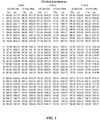
- Fig. 1 The channel plans specified for three of these bands (L-, C- and S-Bands) are set forth in Fig. 1 . It can be seen that channels are defined at 50GHz intervals, though a typical system would use channels at 100GHz spacing: either on multiples of 100GHz or at a 50GHz offset from multiples of 100GHz.
- the ITU grid shows as many as 50 channels usable in each band, for some applications it is desirable to carry channels in two or more bands.
- AWGs in a bidirectional transmission system, with one band of frequencies for upstream traffic, from ONU to OLT, and another band of frequencies for downstream traffic, from OLT to ONU.
- This can be achieved by using two separate AWGs on each end of the transmission path, one designed for each of the two bands.
- the multiplexed outputs of the two AWGs on one end are either carried separately to the other end on two separate fibers, or are combined onto a single fiber using a WDM filter/combiner.
- WDM filter/combiner it would be preferable if a single AWG could suffice on each end. It is possible to use a single AWG to multiplex/demultiplex signals in more than one band, but a number of problems arise.
- the channel spacing is proportional to the order addressed by the AWG.
- designs have been made which can be deployed in both the C-band and L-band using order 38 and order 37 respectively.
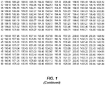
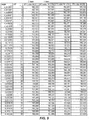
- Fig. 2 is a table illustrating the channel plans of two different AWGs, both using Silica on Silicon technologies but slightly different doping levels.
- One technology achieves a 0.7% contrast between core and cladding and the other achieves a 1.5% index-contrast between core and cladding.
- the 0.7% contrast technology has waveguides with a 6x6um core and the 1.5% technology has waveguides which are 4um square.
- both AWGs are designed for 100GHz on-grid channel spacing on order 38 in the C-band. But the resulting LB and channel plans are different.
- the L-band channels for the higher contrast technology is 24 GHz higher than for low contrast technology. Therefore a WDM-PON AWG made in one technology will not be compatible in the L-band with a WDM-PON AWG made in the other technology. This is one of the reasons why it has been difficult to define an industry standard for the channel plan for WDM-PON telecom systems.
- that plan will soon become obsolete as future improvements in manufacturing technologies dictate still different channel plans for the second channel.
- the invention involves arrayed waveguide grating apparatus having an input free-space region, an output free-space region, and an array of waveguides from the input free-space region to the output free-space region, wherein the input free-space region has an input port comprising at least first and second inputs, wherein the output free-space region has an output port comprising a plurality of outputs, wherein the first and second input ports address respectively first and second different orders M 1 and M 2 of the waveguide array, wherein the plurality of outputs and the first input are disposed such that optical energy provided on the first input will appear on the outputs with a first center frequency v 1 N 1 and first channel spacing ⁇ (v 1 N 1 ) among the outputs, N 1 being the effective index of refraction of a waveguide in the waveguide array at frequency v 1 , the outputs being positioned for constant channel spacing between each pair of adjacent ones of the plurality of outputs when operated at the first center frequency, and wherein the second input is disposed such that optical energy provided
- the first and second center frequencies may be in different ones of the ITU-defined frequency bands, for example in respectively the C-band and L-band. As another example, they may be located in two different sub-bands of a single one of the ITU-defined frequency bands.
- the first and second channel spacings are substantially equal to each other. Preferably they are both equal to 50GHz, and the first and second center frequencies both lie substantially on multiples of 50GHz. In another embodiment, the first and second channel spacings are both substantially equal to 50GHz and the first and second center frequencies both lie on multiples of 50GHz. In yet another embodiment, the first and second channel spacings are both substantially equal to 50GHz and the first and second center frequencies both lie substantially on multiples of 50GHz.
- the AWGs are operated so as to carry channels from both bands simultaneously.
- the AWGs may also be implemented in a system that includes a first AWG having a plurality of inputs and a set of at least first and second outputs and a second AWG having at least first and second inputs and a plurality of outputs, for use with a transmission path carrying first optical energy from the first output of the first AWG to the first input of the second AWG and from the second output of the first AWG to the second input of the second AWG.
- the first and second outputs of the first AWG address respectively first and second different orders of the first AWG such that optical energy carried on the first output of the first AWG has a plurality of channels having first desired channel spacing and a first desired center frequency and at the same time optical energy carried on the second output of the first AWG has a plurality of channels having second desired channel spacing and a second desired center frequency.
- the first and second inputs of the second AWG address respectively first and second different orders of the second AWG such that optical energy carried on the first input of the second AWG has a plurality of channels having the first channel spacing and the first center frequency and at the same time optical energy carried on the second input of the second AWG has a plurality of channels having the second channel spacing and the second center frequency.
- the first and second AWGs may be fabricated with the same or different technology parameters, and the first and second orders on which the first AWG is operated need not match the first and second orders on which the second AWG is operated.
- the different technology parameters may include different materials, different waveguide dispersions, and different sums of material and waveguide dispersion.
- the transmission path includes two optical fibers, one carrying the first optical energy and the other carrying the second optical energy.
- the transmission path has only a single optical fiber.
- the system in this configuration further includes a first WDM filter/combiner having two inputs in optical communication with respectively the first and second outputs of the first AWG and an output in communication with a first end of the single optical fiber, and a second WDM filter/combiner having one input in communication with a second end of the single optical fiber and two outputs in optical communication with respectively the first and second inputs of the second AWG.
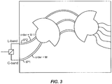
- the present technology addresses the above limitations, in one or more improvements, separately or together. It allows an AWG to be designed using any set of technology parameters which will multiplex or demultiplex channels in two or more frequency bands or sub-bands simultaneously, having virtually any desired frequency spacing between the bands or sub-bands, and virtually any desired channel spacing inside each of the bands or sub-bands. For example, it allows definition of a channel plan on two different bands simultaneously with almost identical channel spacing in one band as in the other. It also allows design of an AWG with arbitrary separation between two frequency bands simultaneously. In practice it is often desired to have all the frequencies to be multiples of 50 GHz, thereby maintaining compatibility with the existing ITU grid. Roughly described, the present technology achieves this using a dual input AWG as shown in Fig. 3 , instead of a single input AWG. Other embodiments have multiple inputs of three or more.
- One of the inputs is used for one band of frequencies, say the C-band, and the other input carries the other band of frequencies, say the L-band.
- an AWG is designed which operates in the blue and red sub-bands of the C-band respectively.
- the sub bands can be defined arbitrarily. Although the industry has not yet decided what bands of frequencies will be used for WDM-PON, the technology disclosed herein is applicable to any combination of sub-bands from any combination of bands. For example it could be S-band and C-band, or C-band and L-band or any sub-band of C-band and any sub-band of L-band.
- the ITU standard the frequencies being multiples of 50 GHz, is currently used in DWDM telecom systems.
- the present technology is applicable to multiples other than 50 GHz, higher than 50 GHZ or lower than 50 GHz.
- Prior art instances of dual input cyclic AWGs operate on one sub-band at a time, because they were developed as an inventory reduction alternative to single input cyclic AWG. These AWGs can operate with one selectable sub-band at a time, but not multiple sub-bands simultaneously.
- the reason for this limitation with prior art AWGs is that only one sub-band at a time is required to maintain compatibility with the telecom system which uses the single input AWG.
- Problems with ITU wavelength error are acknowledged but remain unresolved, such as in US Patent No. 6,608,948 .
- techniques such as different temperature set point, stressing devices, and moving input position are used to shift the center frequency depending on the frequency band for which it is to be deployed. In the case of a dual input AWG these techniques shift the center frequency of both inputs simultaneously, so if they are adjusted to provide correct channel spacing or center frequency for one band, they would not be accurate for the other band.
- an angular displacement of the input will shift the frequency of the L-band or red frequencies relative to the C-band or blue frequencies.
- the displacement is angular.
- this shift of the input allows one to freely design the frequency separation between the two bands.
- the displacement of the input also modifies the channel-spacing.
- the combined change of channel spacing, a decrease due to operation in a lower order for the L-band or red frequencies, and an increase or decrease in channel spacing due to the displacement of the input results in almost any arbitrary channel spacing, as desired.
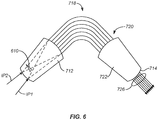
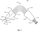
- Fig. 7 illustrates an AWG incorporating features of the invention. It comprises a substrate ("die”, “chip”) 700 supporting two or more input optical waveguides 710 delivering optical energy into an "input slab” region 712. Two specific inputs IP1 and IP2 are shown.
- the slab region 712 is a planar waveguide which confines the input optical energy in only the vertical dimension; the energy is permitted to spread transversely without restriction.
- the input slab is sometimes referred to herein as an "input free space region", or an “input free propagation region”. Note that despite the implication of these terms, energy spreads freely in these regions only in the transverse dimension; it remains confined vertically.
- a far field image of the input optical energy for each of the inputs is developed on the far boundary 714 of the input free space region 712. At this boundary the light enters the input end 716 of a waveguide array 718 which consists of tens or hundreds of individual waveguides.
- the array waveguides are of lengths which increase linearly across the array, each waveguide having a length which differs from its nearest adjacent waveguide by a value ⁇ L.
- the output slab region is a planar waveguide which confines the input optical energy in only the vertical dimension. The energy is permitted to spread transversely without restriction, and for that reason the output slab is sometimes referred to herein as an "output free space region", or an "output free propagation region".
- the input and output free space regions overlap each other such that the input and output beams cross each other. Note that it is assumed herein that the input and output free-space region have identical refractive index. The formulas set forth herein can be easily modified accordingly if this is not the case in a particular embodiment.
- a diffraction pattern is developed on the far boundary 724 of the output free space region 722, where the light enters a set of one or more output optical waveguides 726.
- the structure can be used as a demultiplexer for WDM signals carried on IP1.
- information can be carried on multiple channels (wavelengths) in IP1 and the channels are separated out by the AWG for delivery into the different output waveguides 726.
- the structure can also be used as a multiplexer if operated in reverse.
- the terms "input” and “output” are used only to distinguish between the two ends of the device, and not to indicate which direction the light travels. That is, a particular device might include two ports A and B. If used in one way, light may travel from port A to port B whereas if operated in reverse, light may travel from port B to port A. As used herein, port A may be called the “input” and port B the “output”, but this does not preclude operating the device in such a way that light travels from port B to port A. In fact in many embodiments herein, light travels in both directions simultaneously. Thus description herein describes the structure of the device, which does not change if operated with light traveling in the opposite direction.
- the waveguides of the waveguide array 718 and the output waveguides input or output waveguides 710 or 726 can merely terminate at positions corresponding to the arcs that are shown in Fig. 7 as forming the boundaries of the free space regions 712 and 722 respectively.
- the arcs on which they terminate are referred to herein as "boundaries", whether or not the arc is manifested as an arc physically in the device.
- the upstream and downstream boundaries of the free-space regions are shown in Fig. 7 as having an arc shape, an arc shape is not required in all embodiments.
- optical energy provided on one of the inputs IP1 carrying signals on multiple wavelengths are separated out by the AWG for delivery into the different output waveguides 726.
- the well-known grating equation is typically used to determine where to position the receivers for the output waveguides 726.
- the grating equation gives the positions of the receivers as angular offsets from the array centerline in the output free space region 722, and they depend on technology parameters of the device (such as the pitch d a of the array 718 waveguides where they meet the free space regions, and the effective indices of refraction of the free space regions and the array waveguides (both of which depend on the channel frequency)), the path length increment ⁇ L between adjacent waveguides in the array 718, the order M at which the AWG is operated, and the frequency of the particular channel which is to be captured by each receiver.
- each output waveguide 726 carries two channels: one in each band.
- the channels would not appear at the same angular positions as required for the channels of the first band. It may be possible to operate the second band on a different order, but in order to match the angular positions appropriate for the first band, as explained previously the channel plan of the second band will not be as desired. In particular the second band would have a disadvantageous frequency spacing.
- the AWG of Fig. 7 includes a second input IP2 on which the second band of frequencies can be carried.
- the first and second inputs are disposed across the input free-space region from the array at angles ⁇ IP1 and ⁇ IP2 measured relative to where the array centerline meets the input free-space region 712.
- the "array centerline" curves with the waveguide array itself, but is considered to continue in straight lines both upstream and downstream of the array 718. The straight lines are the tangents to the array centerline where the array terminates.
- the array centerline upstream of the array is not usually in-line with the array centerline downstream of the array.
- the array centerline, as it extends into the input slab region 712, is designated 730.
- input and output angles ⁇ IP and ⁇ OP are defined with the conventions shown in Fig. 14 .
- v 1 is the desired center frequency of the IP1 frequency band and v 2 is the desired center frequency of the IP2 frequency band
- d a is a pitch of the array waveguides where they meet the input free space region
- c is the speed of light in a vacuum
- N s1 is the effective index of refraction in the input free space region at frequency v 1
- N s2 is the effective index of refraction in the input free space region at frequency v 2
- M 1 is the order on which input IP1 operates
- M 2 is the order on which input IP2 operates.
- N 1 is the effective index of refraction of a waveguide in the waveguide
- Fig. 9 is a table showing a channel plan that matches the ITU-plan, within a few GHz, for both the C-band and the L-band.
- This channel plan is made for the high contrast technology described above, 1.5% index-contrast between core and cladding, but one could make a channel plan equally close to the ITU grid using the low contrast glass technology described above, with 0.7% index contrast.
- a red-blue channel plan which is within a few Ghz ( ⁇ 2 GHz) on the ITU grid for both the red band and the blue band can be achieved as shown in the table of Fig. 10 .
- the design is made for an AWG which operates on order 40 for input IP1, the blue band, and on order 39 for input IP2, the red band.
- This design is made for a technology where the index-contrast between the 4x4 um glass core and the cladding is 1.5%.
- the effective index of the waveguide in the AWG-array section is 1.4568, and the effective index in the slab is 1.4624.
- the angle of input IP1 is -0.05298 radian and the angle of input IP2 is 0.05298 radian.
- the angles of the outputs are shown in Fig. 8 .
- the channel plans for input IP1 and input IP2 overlap. This allows the use of many more channels than would be possible with a single input AWG.
- a band-filter a so called red-blue filter
- outputs 13-36 to have a red-band that goes from 191.7 THz to 194.0 THz and a blue band that goes from 194.1 THz to 196.4 THz.
- the same dual AWG can equally be split differently, e.g. 191.6 THZ to 193.9 THz for the red C-band and 194.0 THz to 196.3 THz for the blue C-band.
- the angles of the two inputs are not centered about zero. This is not a requirement in all embodiments. Due to technology variation, it could occur that the separation between the two bands, the blue and red band, is not exactly a multiple of 100 GHz, in which case one could empirically correct for this by angularly shifting one input relative to the other. Such a correction could also be achieved by UV or heat trimming, that is creating a high or low index region in the shape of a triangle or other geometries.
- One example configuration of a different index region is given in Fig. 6 , where a high index region 610 has been inserted in only the optical paths for input IP2.
- the dual input AWG can be athermalised by any of the same techniques as for single input AAWG. See for example the above-incorporated U.S. Patent No. 7,397,986 .
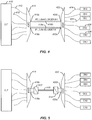
- FIGs. 4 and 5 illustrate systems having AWGs incorporating aspects of the invention on both ends of a transmission line.
- an OLT (Optical Line Terminal) 410 has multiple outputs 412 each carrying two channels, one in one band (for example the C-band) and one in a second band (for example the L-band).
- the OLT outputs 412 are connected by fiber to an AWG 414 in multiplexer configuration, such that there are multiple inputs and two outputs 416a and 416b.
- the AWG 414 operates on order M and output 416a carries all the C-band channels from all the OLT 410 outputs 412.
- the AWG operates on a different order, in this illustration order M-1, and output 416b carries all the L-band channels from all the OLT 410 outputs 412. All the signals are carried on a transmission path consisting of two separate fibers 418a and 418b to two corresponding inputs 420a and 420b of another two-input AWG 422 in the field in a demultiplexer configuration.
- AWG 422 has multiple outputs 424, corresponding to the multiple outputs 412 of the OLT 410, and these are connected by fiber to respective ONUs (optical network units) 426 near the end users.
- Each fiber 424 carries two channels, one in the C-band and one in the L-band. Typically, one of these channels are used for upstream traffic while the other channel is used for downstream traffic. The two can operate simultaneously.
- Fig. 5 is the same as Fig. 4 , except that the transmission path which consisted in Fig. 4 of two fibers 418a and 418b, has been replaced by a transmission path that consists of a single fiber 510, connected at one end to AWG 414 via a WDM filter/combiner 512, and connected at the other end to AWG 422 via another WDM filter/combiner 514.
- the WDM filter/combiner 512 combines the C-band channels on AWG 414 output 416a with the L-band channels on AWG 414 output 416b, onto the single fiber 510.
- the WDM filter/combiner 514 splits the two bands from fiber 510, communicating the C-band channels to input 420a of AWG 422 and communicating the L-band channels to input 420b of AWG 422.
- Fig. 4 In the configuration of Fig. 4 , one does not require a WDM band filter, to separate the frequency bands for the two inputs on the AWG at the ONU side. Nor for the two outputs when this dual AWG is operated in reverse, i.e. as a multiplexer on the OLT side of a WDM-PON network. In that situation, one uses two fibers, one fiber for each input/frequency band, for example using one input/band for upstream and another for downstream traffic. The channel plans of the two frequency bands can partially overlap and depending on further system requirements, one could use the overlapping frequencies, to increase capacity in the system.
- the configuration of Fig. 5 requires only a single fiber in the transmission path.
- N a is the effective index of an array waveguide and N s is the effective index of the slab.
- N a is sometimes written herein merely as N.
- the central wavelength ⁇ c or central frequency v c for that matter, is a property of the array section, and corresponds to the frequency for which M times the wavelength exactly makes up the path difference. I.e. it is the frequency, for a given order M, where the angle of the input and output beam are exactly equal, but of opposite sign.
- FSR free spectral range
- the free spectral range defines the repetition rate of the spectral response in the frequency domain.
- the FSR varies for the different outputs.
- FSR is defined here for the output which has equal but opposite angle as the input waveguide.
- the FSR depends on the material and waveguide dispersion dN d ⁇ or ⁇ .
- dN d ⁇ or ⁇ In the telecom C-band ⁇ is 0.9793 for the 1.5% contrast 4x4um technology and ⁇ equals 0.984 for the 0.7% contrast 6x6 um Silica on Silicon technology.
- ⁇ output v arcsin ⁇ L d a N v N s v 1 ⁇ v c N v c vN v ⁇ sin ⁇ input .
- the AWG is designed such that two bands of frequencies are mixed on the output side, both of which can be made to match the ITU grid. This is achieved by using two inputs, each of which addresses one band and where each frequency band corresponds to a different order. These channel plans are impossible to achieve with a conventional cyclic AWG using only a single input. It is noted that the above can be extended beyond two bands, by using more than 2 inputs and more than 2 orders.
- the order of an AWG addressed by each of the inputs is a physical characteristic of the device. It can be determined from an AWG by performing a frequency scan of the device, or by calculation given the technology parameters of the device and the path length increment between adjacent waveguides in the array.
- M 1 v 1 M 2 N 1 M 2 M 2 v 1 M 1 N 1 M 1 where M 1 is one integer order, and M 2 another.
- v 1 M 2 is the frequency from input 1 operating on order M 2
- v 1 M 1 and is the frequency from input 1 operating on order M 1
- N 1 M 2 is the array index at frequency v 1 M 2
- N 1 M 1 is the array index at frequency v 1 M 1 .
- Fig. 13 reproduces the technology specific channel plans mentioned earlier and as shown in the table of Fig. 2 .
- ⁇ v 1 100 GHz for input 1
- ⁇ v 2 97.37 Ghz for input 2.
- Another benefit of the multi-input AWGs here described over a single input cyclic AWG is that the two inputs can each have empirical corrections. For example by UV-writing prisms in the path of each beam (triangular regions of different index) or moving one input relative to the other(s) by other means.
- the model equation gives solutions for M 1 and M 2 , v 1 and v 2 , etc.
- ⁇ v arcsin ⁇ L d a N v N s v 1 ⁇ v c N v c vN v ⁇ sin ⁇ input , where it should be noted that v c itself depends on the grating order, M 1 for input 1, and M 2 for input 2, and so on for cases of more than 2 inputs.
- the grating equation is used to determine the length increment ⁇ L between adjacent waveguides in the array.
- the grating equation is used to calculate the required angles for all the output receivers. This calculation can be done for either of the inputs since both should yield the same angles for the output receivers.
Landscapes
- Physics & Mathematics (AREA)
- Engineering & Computer Science (AREA)
- Microelectronics & Electronic Packaging (AREA)
- General Physics & Mathematics (AREA)
- Optics & Photonics (AREA)
- Optical Integrated Circuits (AREA)
- Optical Communication System (AREA)
- Aerials With Secondary Devices (AREA)
Description
- Applicants hereby claim the benefit under 35 U.S.C. 119(e) of
U.S. provisional application No. 61/392,131, filed 12 October 2010 - The invention relates generally to optical waveguide grating devices, and more particularly to a device that simultaneously supports more than one frequency band with accurate channel spacing.
- Computer and communication systems place an ever-increasing demand upon communication link bandwidths. It is generally known that optical fibers offer a much higher bandwidth than conventional coaxial links. Further, a single optical channel in a fiber waveguide uses a small fraction of the available bandwidth of the fiber. In wavelength division multiplexed (WDM) optical communication systems, multiple optical wavelength carriers transmit independent communication channels along a single optical fiber. By transmitting several channels at different wavelengths into one fiber, the bandwidth capability of an optical fiber is efficiently utilized.
- Fiber-optic multiplexing and demultiplexing have been accomplished using an arrayed waveguide grating (AWG) device. An AWG is a planar structure comprising an array of waveguides disposed between input and output couplers and arranged side-by-side with each other, and which together act like a diffraction grating in a spectrometer. Each of the waveguides differs in length with respect to its nearest neighbor by a predetermined fixed amount. The outputs of the output coupler form the outputs of the multiplexing and demultiplexing device. In operation, when a plurality of separate and distinct wavelengths are applied to separate and distinct input ports of the device, they are combined and are transmitted to an output port. The same device may also perform a demultiplexing function in which a plurality of input wavelengths on one input port of the apparatus, are separated from each other and directed to predetermined different ones of the output ports. AWGs can also perform a routing function, in which signals arrive on multiple input ports and are routed to multiple different output ports in accordance with a predefined mapping. The construction and operation of such AWGs is well known in the art. See for example, "PHASAR-based WDM-Devices: Principles, Design and Applications", M K Smit, IEEE Journal of Selected Topics in Quantum Electronics Vol.2, No.2, June 1996;
U.S. Patents 5,002,350 ;7,397,986 ;7,492,991 ; andWO97/23969 -
US 2004/0264857 describes an arrayed waveguide grating (AWG) with improved transmission efficiency including an input PxM star coupler, an output MxQ star coupler, and M waveguides of unequal length connecting the input and output star couplers. - AWGs are often used in WDM-PON (wavelength division multiplexing passive optical network) systems. A typical PON has an optical line terminal (OLT) at the service provider's central office and a number of optical network units (ONUs) near end users. Each OLT and ONU includes one or more AWGs, so that multiple channels on different transmission frequencies can be carried on a single fiber. The AWGs multiplex the channels from multiple inputs at one end, and demultiplex them into multiple outputs at the other end. In order to permit such systems to be deployed with AWGs from a variety of vendors, several wavelength "bands" have been defined, and the channel spacing within each band has also been defined. These definitions have been incorporated into standards mainly under the auspices of the International Telecommunications Union (ITU). The following spectral bands have been defined in ITU specifications:
Band Descriptor Range [nm] O-band Original 1260 to 1360 E-band Extended 1360 to 1460 S-band Short wavelength 1460 to 1530 C-band Conventional / Center 1530 to 1565 L-band Long wavelength 1565 to 1625 U-band Ultra long wavelength 1625 to 1675 - The channel plans specified for three of these bands (L-, C- and S-Bands) are set forth in
Fig. 1 . It can be seen that channels are defined at 50GHz intervals, though a typical system would use channels at 100GHz spacing: either on multiples of 100GHz or at a 50GHz offset from multiples of 100GHz. - Though the ITU grid shows as many as 50 channels usable in each band, for some applications it is desirable to carry channels in two or more bands. For example, it is often proposed in literature to use AWGs in a bidirectional transmission system, with one band of frequencies for upstream traffic, from ONU to OLT, and another band of frequencies for downstream traffic, from OLT to ONU. This can be achieved by using two separate AWGs on each end of the transmission path, one designed for each of the two bands. The multiplexed outputs of the two AWGs on one end are either carried separately to the other end on two separate fibers, or are combined onto a single fiber using a WDM filter/combiner. However, it would be preferable if a single AWG could suffice on each end. It is possible to use a single AWG to multiplex/demultiplex signals in more than one band, but a number of problems arise.
- First, in a conventional AWG, the channel spacing is proportional to the order addressed by the AWG. For example, designs have been made which can be deployed in both the C-band and L-
band using order 38 andorder 37 respectively. But if the design addresses the ITU-grid with channel spacing of 100 GHz using AWG-order 38 in the C-band, then the same AWG would have a channel spacing of 37/38*100=97.4 GHz, operating onorder 37, in the L-band. It would deviate from the ITU specification and therefore be incompatible with AWGs on the far end of the transmission path that are designed for the standard 100GHz spacing. - It has consequently been proposed to change the ITU specification to allow an off-grid channel spacing for the second band. But this creates another problem in that it is difficult to standardize the second channel plan. This is due to the fact that the two bands of frequencies, in particular the separation between the two bands, is defined by technology parameters used in the manufacture of the AWG, such as the material and waveguide dispersion, which vary from manufacturer to manufacturer.
- To illustrate this point,
Fig. 2 is a table illustrating the channel plans of two different AWGs, both using Silica on Silicon technologies but slightly different doping levels. One technology achieves a 0.7% contrast between core and cladding and the other achieves a 1.5% index-contrast between core and cladding. The 0.7% contrast technology has waveguides with a 6x6um core and the 1.5% technology has waveguides which are 4um square. For these two technologies, for wavelength around 1550 nm, the sum of material and waveguide dispersion are given by

- It can be seen that both AWGs are designed for 100GHz on-grid channel spacing on
order 38 in the C-band. But the resulting LB and channel plans are different. The L-band channels for the higher contrast technology is 24 GHz higher than for low contrast technology. Therefore a WDM-PON AWG made in one technology will not be compatible in the L-band with a WDM-PON AWG made in the other technology. This is one of the reasons why it has been difficult to define an industry standard for the channel plan for WDM-PON telecom systems. Furthermore, even if all manufacturers can agree on one off-grid channel plan for the second frequency band, that plan will soon become obsolete as future improvements in manufacturing technologies dictate still different channel plans for the second channel. - Particular and preferred aspects of the present invention are set out in the accompanying independent and dependent claims.
- An opportunity therefore arises to develop ways to design a single AWG which operates at the correct channel spacing in two or more frequency bands simultaneously.
- Roughly described, the invention involves arrayed waveguide grating apparatus having an input free-space region, an output free-space region, and an array of waveguides from the input free-space region to the output free-space region, wherein the input free-space region has an input port comprising at least first and second inputs, wherein the output free-space region has an output port comprising a plurality of outputs, wherein the first and second input ports address respectively first and second different orders M1 and M2 of the waveguide array, wherein the plurality of outputs and the first input are disposed such that optical energy provided on the first input will appear on the outputs with a first center frequency v1N1 and first channel spacing Δ(v1N1) among the outputs, N1 being the effective index of refraction of a waveguide in the waveguide array at frequency v1, the outputs being positioned for constant channel spacing between each pair of adjacent ones of the plurality of outputs when operated at the first center frequency, and wherein the second input is disposed such that optical energy provided on the second input will appear on the plurality of outputs with a desired second center frequency v2N2 and second channel spacing Δ(v2N2) among the outputs.
- Preferably, the first and second inputs are disposed across the input free-space region from the array at angles θ IP1 and θ IP2 measured relative to where the array centerline meets the input free-space region,
where θ IP1 and θ IP2 substantially satisfy
where c is the speed of light, and where Ns1 is the effective index of refraction in the input free space region at frequency v1, Ns2 is the effective index of refraction in the input free space region at frequency v2, N1 the effective index of refraction of a waveguide in the waveguide array at frequency v1, N2 the effective index of refraction of a waveguide in the waveguide array at frequency v2,
and where Δ(v1N1)/ Δ(v2N2) substantially satisfies

- The first and second center frequencies may be in different ones of the ITU-defined frequency bands, for example in respectively the C-band and L-band. As another example, they may be located in two different sub-bands of a single one of the ITU-defined frequency bands.
- Preferably the first and second orders are related as M2 = M1-1.
- In an embodiment, the first and second channel spacings are substantially equal to each other. Preferably they are both equal to 50GHz, and the first and second center frequencies both lie substantially on multiples of 50GHz. In another embodiment, the first and second channel spacings are both substantially equal to 50GHz and the first and second center frequencies both lie on multiples of 50GHz. In yet another embodiment, the first and second channel spacings are both substantially equal to 50GHz and the first and second center frequencies both lie substantially on multiples of 50GHz.
- The AWGs are operated so as to carry channels from both bands simultaneously.
- The AWGs may also be implemented in a system that includes a first AWG having a plurality of inputs and a set of at least first and second outputs and a second AWG having at least first and second inputs and a plurality of outputs, for use with a transmission path carrying first optical energy from the first output of the first AWG to the first input of the second AWG and from the second output of the first AWG to the second input of the second AWG. The first and second outputs of the first AWG address respectively first and second different orders of the first AWG such that optical energy carried on the first output of the first AWG has a plurality of channels having first desired channel spacing and a first desired center frequency and at the same time optical energy carried on the second output of the first AWG has a plurality of channels having second desired channel spacing and a second desired center frequency. Similarly, the first and second inputs of the second AWG address respectively first and second different orders of the second AWG such that optical energy carried on the first input of the second AWG has a plurality of channels having the first channel spacing and the first center frequency and at the same time optical energy carried on the second input of the second AWG has a plurality of channels having the second channel spacing and the second center frequency. The first and second AWGs may be fabricated with the same or different technology parameters, and the first and second orders on which the first AWG is operated need not match the first and second orders on which the second AWG is operated. The different technology parameters may include different materials, different waveguide dispersions, and different sums of material and waveguide dispersion.
- In one configuration the transmission path includes two optical fibers, one carrying the first optical energy and the other carrying the second optical energy.
- In another configuration the transmission path has only a single optical fiber. The system in this configuration further includes a first WDM filter/combiner having two inputs in optical communication with respectively the first and second outputs of the first AWG and an output in communication with a first end of the single optical fiber, and a second WDM filter/combiner having one input in communication with a second end of the single optical fiber and two outputs in optical communication with respectively the first and second inputs of the second AWG.
- The above summary of the invention is provided in order to provide a basic understanding of some aspects of the invention. This summary is not intended to identify key or critical elements of the invention or to delineate the scope of the invention. Its sole purpose is to present some concepts of the invention in a simplified form as a prelude to the more detailed description that is presented later. Particular aspects of the invention are described in the claims, specification and drawings.
- The invention will be described with respect to specific embodiments thereof, and reference will be made to the drawings, in which:
-
Fig. 1 is a table of a portion of the ITU Grid Specification. -
Fig. 2 is a table illustrating channel plans of two different AWGs made with different technology parameters. -
Figs. 3 ,6 and7 illustrate AWGs incorporating features of the invention. -
Figs. 4 and 5 illustrate systems having AWGs incorporating aspects of the invention on both ends of a transmission path. -
Fig. 8 sets forth angles of outputs of an AWG. -
Fig. 9 is a table showing a channel plan that matches the ITU-plan, within a few GHz, for both the C-band and the L-band. -
Fig. 10 is a table showing a red-blue channel plan which is very close to the ITU grid for both the red band and the blue band. -
Figs. 11-13 are charts illustrating results that can be achieved using aspects of the invention. -
Fig. 14 is a drawing which defines angle conventions for an AWG. - The following description is presented to enable any person skilled in the art to make and use the invention, and is provided in the context of a particular application and its requirements. Various modifications to the disclosed embodiments will be readily apparent to those skilled in the art, and the general principles defined herein may be applied to other embodiments and applications without departing from the scope of the present invention. Thus, the present invention is not intended to be limited to the embodiments shown, but is to be accorded the widest scope consistent with the principles and features disclosed herein.
- The present technology addresses the above limitations, in one or more improvements, separately or together. It allows an AWG to be designed using any set of technology parameters which will multiplex or demultiplex channels in two or more frequency bands or sub-bands simultaneously, having virtually any desired frequency spacing between the bands or sub-bands, and virtually any desired channel spacing inside each of the bands or sub-bands. For example, it allows definition of a channel plan on two different bands simultaneously with almost identical channel spacing in one band as in the other. It also allows design of an AWG with arbitrary separation between two frequency bands simultaneously. In practice it is often desired to have all the frequencies to be multiples of 50 GHz, thereby maintaining compatibility with the existing ITU grid. Roughly described, the present technology achieves this using a dual input AWG as shown in
Fig. 3 , instead of a single input AWG. Other embodiments have multiple inputs of three or more. - One of the inputs is used for one band of frequencies, say the C-band, and the other input carries the other band of frequencies, say the L-band. In another example, an AWG is designed which operates in the blue and red sub-bands of the C-band respectively. The sub bands can be defined arbitrarily. Although the industry has not yet decided what bands of frequencies will be used for WDM-PON, the technology disclosed herein is applicable to any combination of sub-bands from any combination of bands. For example it could be S-band and C-band, or C-band and L-band or any sub-band of C-band and any sub-band of L-band. The ITU standard, the frequencies being multiples of 50 GHz, is currently used in DWDM telecom systems. It is expected to use those same frequencies in any future telecom architectures, like WDM-PON, as well. This is because it enables the use of existing components. However, in other embodiments, the present technology is applicable to multiples other than 50 GHz, higher than 50 GHZ or lower than 50 GHz.
- Prior art instances of dual input cyclic AWGs operate on one sub-band at a time, because they were developed as an inventory reduction alternative to single input cyclic AWG. These AWGs can operate with one selectable sub-band at a time, but not multiple sub-bands simultaneously. The reason for this limitation with prior art AWGs, is that only one sub-band at a time is required to maintain compatibility with the telecom system which uses the single input AWG. Problems with ITU wavelength error are acknowledged but remain unresolved, such as in
US Patent No. 6,608,948 . In such designs techniques such as different temperature set point, stressing devices, and moving input position are used to shift the center frequency depending on the frequency band for which it is to be deployed. In the case of a dual input AWG these techniques shift the center frequency of both inputs simultaneously, so if they are adjusted to provide correct channel spacing or center frequency for one band, they would not be accurate for the other band. - Indeed, the approach described herein can be extended to more than two inputs for more than two frequency bands. But in current applications, like WDM-PON two bands of frequencies is most relevant.
- As will be shown mathematically in a later section, an angular displacement of the input will shift the frequency of the L-band or red frequencies relative to the C-band or blue frequencies. The displacement is angular. Hence, this shift of the input allows one to freely design the frequency separation between the two bands. On top of that, and more importantly, it is known that the displacement of the input also modifies the channel-spacing. The combined change of channel spacing, a decrease due to operation in a lower order for the L-band or red frequencies, and an increase or decrease in channel spacing due to the displacement of the input, results in almost any arbitrary channel spacing, as desired.
- There are three design parameters which can be chosen more or less freely: the order of the frequency band of
input 1, the order of the frequency band ofinput 2, and the angular displacement ofinput 2 relative toinput 1. Apart from the restriction that the order is an integer, this allows the designer to achieve both correct frequency separation of bands AND correct channel spacing. - It is possible to achieve correct channel spacing and almost exact frequency separation (<±2 GHz difference for practical purpose for AWG working with one band in C band and another in L-band) or it is possible to achieve correct frequency separation and almost exact channel spacing, (better than 0.2% for AWG working with one band in C band and another in L-band) or any combination, such as both nearly exact frequency separation and nearly exact channel spacing.
-
Fig. 7 illustrates an AWG incorporating features of the invention. It comprises a substrate ("die", "chip") 700 supporting two or more inputoptical waveguides 710 delivering optical energy into an "input slab"region 712. Two specific inputs IP1 and IP2 are shown. Theslab region 712 is a planar waveguide which confines the input optical energy in only the vertical dimension; the energy is permitted to spread transversely without restriction. The input slab is sometimes referred to herein as an "input free space region", or an "input free propagation region". Note that despite the implication of these terms, energy spreads freely in these regions only in the transverse dimension; it remains confined vertically. - A far field image of the input optical energy for each of the inputs is developed on the
far boundary 714 of the inputfree space region 712. At this boundary the light enters theinput end 716 of awaveguide array 718 which consists of tens or hundreds of individual waveguides. The array waveguides are of lengths which increase linearly across the array, each waveguide having a length which differs from its nearest adjacent waveguide by a value ΔL. - Optical energy exits the
waveguide array 716 at anoutput end 720 thereof, and delivers the light into an "output slab"region 722. Like the input slab, the output slab region is a planar waveguide which confines the input optical energy in only the vertical dimension. The energy is permitted to spread transversely without restriction, and for that reason the output slab is sometimes referred to herein as an "output free space region", or an "output free propagation region". In some embodiments the input and output free space regions overlap each other such that the input and output beams cross each other. Note that it is assumed herein that the input and output free-space region have identical refractive index. The formulas set forth herein can be easily modified accordingly if this is not the case in a particular embodiment. - A diffraction pattern is developed on the far boundary 724 of the output
free space region 722, where the light enters a set of one or more outputoptical waveguides 726. Considering one of theinput waveguides 710, for example IP1, the structure can be used as a demultiplexer for WDM signals carried on IP1. Thus information can be carried on multiple channels (wavelengths) in IP1 and the channels are separated out by the AWG for delivery into thedifferent output waveguides 726. The structure can also be used as a multiplexer if operated in reverse. - Because of the bidirectional nature of the optical components described herein, as used herein, the terms "input" and "output" are used only to distinguish between the two ends of the device, and not to indicate which direction the light travels. That is, a particular device might include two ports A and B. If used in one way, light may travel from port A to port B whereas if operated in reverse, light may travel from port B to port A. As used herein, port A may be called the "input" and port B the "output", but this does not preclude operating the device in such a way that light travels from port B to port A. In fact in many embodiments herein, light travels in both directions simultaneously. Thus description herein describes the structure of the device, which does not change if operated with light traveling in the opposite direction.
- It will be appreciated that while the free space regions are often though of as having structural features to mark their boundaries, in fact in many cases structural features are unnecessary; the waveguides of the
waveguide array 718 and the output waveguides input oroutput waveguides Fig. 7 as forming the boundaries of thefree space regions Fig. 7 as having an arc shape, an arc shape is not required in all embodiments. - As mentioned, optical energy provided on one of the inputs IP1 carrying signals on multiple wavelengths, are separated out by the AWG for delivery into the
different output waveguides 726. The well-known grating equation is typically used to determine where to position the receivers for theoutput waveguides 726. The grating equation gives the positions of the receivers as angular offsets from the array centerline in the outputfree space region 722, and they depend on technology parameters of the device (such as the pitch da of thearray 718 waveguides where they meet the free space regions, and the effective indices of refraction of the free space regions and the array waveguides (both of which depend on the channel frequency)), the path length increment ΔL between adjacent waveguides in thearray 718, the order M at which the AWG is operated, and the frequency of the particular channel which is to be captured by each receiver. - But it is desirable to be able to operate the AWG using channels in two different bands, either traveling in the same direction or in opposite directions, such that each
output waveguide 726 carries two channels: one in each band. Because of the dependency on frequency, though, it can be seen that if the input waveguide IP1 were to also carry channels in a second band on the same order M, the channels would not appear at the same angular positions as required for the channels of the first band. It may be possible to operate the second band on a different order, but in order to match the angular positions appropriate for the first band, as explained previously the channel plan of the second band will not be as desired. In particular the second band would have a disadvantageous frequency spacing. - In order to overcome this problem, the AWG of
Fig. 7 includes a second input IP2 on which the second band of frequencies can be carried. As derived mathematically below, the first and second inputs are disposed across the input free-space region from the array at angles θ IP1 and θ IP2 measured relative to where the array centerline meets the input free-space region 712. As used herein, within thewaveguide array 718 of an AWG, the "array centerline" curves with the waveguide array itself, but is considered to continue in straight lines both upstream and downstream of thearray 718. The straight lines are the tangents to the array centerline where the array terminates. Since thearray 718 is curved, the array centerline upstream of the array is not usually in-line with the array centerline downstream of the array. InFig. 7 , the array centerline, as it extends into theinput slab region 712, is designated 730. For purposes of the present description, input and output angles θ IP and θ OP are defined with the conventions shown inFig. 14 . - If v1 is the desired center frequency of the IP1 frequency band and v2 is the desired center frequency of the IP2 frequency band, then the two input waveguides IP1 and IP2 are disposed at angles θ IP1 and θ IP2 measured relative to the array centerline, where θ IP1 and θ IP2 satisfy

- Furthermore, the ratio of channel spacings for the two bands, Δ(v1N1)/Δ(v2N2), satisfies


- Using the above equations and the grating equation, it is possible to select values for θ IP1, θ IP2, M1, and M2, such that input IP1 carries frequencies in a first band having virtually any desired center frequency v1 and channel spacing Δ(v1N1), and input IP2 carries frequencies in a second band having virtually any other desired center frequency v2 and any channel spacing Δ(v2N2), and the resulting channel plans will appear coincidently on a single plurality of output receivers for
output waveguides 726. The only significant limitation in the precision with which the resulting center frequencies and channel spacings will exactly match desired values is the requirement that the orders be integers. - As an example,
Fig. 9 is a table showing a channel plan that matches the ITU-plan, within a few GHz, for both the C-band and the L-band. This channel plan is made for the high contrast technology described above, 1.5% index-contrast between core and cladding, but one could make a channel plan equally close to the ITU grid using the low contrast glass technology described above, with 0.7% index contrast. The angle of input IP1 is -0.0525485 radian and the angle for input IP2 is 0.0525485 radian. It is noted that input IP1 carries the C-band frequencies which correspond to order M1 = 20 for this AWG. Input IP2 for the L-band frequencies operates on order M2 = 19. These orders are smaller than for many conventional WDM-PON AWGs, e.g. of the table inFig. 2 , which operates onorders - A red-blue channel plan which is within a few Ghz (<±2 GHz) on the ITU grid for both the red band and the blue band can be achieved as shown in the table of
Fig. 10 . The design is made for an AWG which operates onorder 40 for input IP1, the blue band, and onorder 39 for input IP2, the red band. This design is made for a technology where the index-contrast between the 4x4 um glass core and the cladding is 1.5%. For this technology and type of waveguide, the dispersion in the array waveguide in the telecom window is
array 718 waveguides at the slab-array transition is da=5 µm, and the length increment in the AWG is ΔL=41.88 µm. The angle of input IP1 is -0.05298 radian and the angle of input IP2 is 0.05298 radian. The angles of the outputs are shown inFig. 8 . - It is noted that the channel plans for input IP1 and input IP2 overlap. This allows the use of many more channels than would be possible with a single input AWG. In the configuration of
Fig. 5 , described below, one would use a band-filter, a so called red-blue filter, to multiplex and de-multiplex the two frequency bands for carrying by a single fiber. In that case one would no longer use the channels in one band that overlap in the frequency domain with channels in the other band. For example one might use only 24 output channels, outputs 13-36 to have a red-band that goes from 191.7 THz to 194.0 THz and a blue band that goes from 194.1 THz to 196.4 THz. But the same dual AWG can equally be split differently, e.g. 191.6 THZ to 193.9 THz for the red C-band and 194.0 THz to 196.3 THz for the blue C-band. - In each of the above two examples, one for C-band and L-band and the other for Blue and Red bands, the angles of the two inputs are not centered about zero. This is not a requirement in all embodiments. Due to technology variation, it could occur that the separation between the two bands, the blue and red band, is not exactly a multiple of 100 GHz, in which case one could empirically correct for this by angularly shifting one input relative to the other. Such a correction could also be achieved by UV or heat trimming, that is creating a high or low index region in the shape of a triangle or other geometries. One example configuration of a different index region is given in
Fig. 6 , where ahigh index region 610 has been inserted in only the optical paths for input IP2. Alternatively or additionally, the dual input AWG can be athermalised by any of the same techniques as for single input AAWG. See for example the above-incorporatedU.S. Patent No. 7,397,986 . -
Figs. 4 and 5 illustrate systems having AWGs incorporating aspects of the invention on both ends of a transmission line. Referring toFig. 4 , an OLT (Optical Line Terminal) 410 hasmultiple outputs 412 each carrying two channels, one in one band (for example the C-band) and one in a second band (for example the L-band). The OLT outputs 412 are connected by fiber to anAWG 414 in multiplexer configuration, such that there are multiple inputs and twooutputs output 416a, theAWG 414 operates on order M andoutput 416a carries all the C-band channels from all theOLT 410 outputs 412. Foroutput 416b, the AWG operates on a different order, in this illustration order M-1, andoutput 416b carries all the L-band channels from all theOLT 410 outputs 412. All the signals are carried on a transmission path consisting of twoseparate fibers corresponding inputs input AWG 422 in the field in a demultiplexer configuration.AWG 422 hasmultiple outputs 424, corresponding to themultiple outputs 412 of theOLT 410, and these are connected by fiber to respective ONUs (optical network units) 426 near the end users. Eachfiber 424 carries two channels, one in the C-band and one in the L-band. Typically, one of these channels are used for upstream traffic while the other channel is used for downstream traffic. The two can operate simultaneously. -
Fig. 5 is the same asFig. 4 , except that the transmission path which consisted inFig. 4 of twofibers single fiber 510, connected at one end toAWG 414 via a WDM filter/combiner 512, and connected at the other end toAWG 422 via another WDM filter/combiner 514. The WDM filter/combiner 512 combines the C-band channels onAWG 414output 416a with the L-band channels onAWG 414output 416b, onto thesingle fiber 510. The WDM filter/combiner 514 splits the two bands fromfiber 510, communicating the C-band channels to input 420a ofAWG 422 and communicating the L-band channels to input 420b ofAWG 422. - In the configuration of
Fig. 4 , one does not require a WDM band filter, to separate the frequency bands for the two inputs on the AWG at the ONU side. Nor for the two outputs when this dual AWG is operated in reverse, i.e. as a multiplexer on the OLT side of a WDM-PON network. In that situation, one uses two fibers, one fiber for each input/frequency band, for example using one input/band for upstream and another for downstream traffic. The channel plans of the two frequency bands can partially overlap and depending on further system requirements, one could use the overlapping frequencies, to increase capacity in the system. The configuration ofFig. 5 , on the other hand, requires only a single fiber in the transmission path. - The grating equation: For an AWG, simplified in
figure 1 , the following relation holds
- The central wavelength λc , or central frequency vc for that matter, is a property of the array section, and corresponds to the frequency for which M times the wavelength exactly makes up the path difference. I.e. it is the frequency, for a given order M, where the angle of the input and output beam are exactly equal, but of opposite sign.

- The free spectral range, FSR, can be calculated from the grating equation and is given by:

- The free spectral range defines the repetition rate of the spectral response in the frequency domain. Note that for any cyclic AWG, the FSR varies for the different outputs. In the above equation FSR is defined here for the output which has equal but opposite angle as the input waveguide. Also note that the FSR depends on the material and waveguide dispersion

- The deflection of the focal spot of the array output as a function of frequency is given by:

- Using the above equations, one can engineer arbitrary channel plan for both bands of frequencies.
- In the two example designs set forth above, one for L-band and C-band, and one for red and blue bands of frequencies, the AWG is designed such that two bands of frequencies are mixed on the output side, both of which can be made to match the ITU grid. This is achieved by using two inputs, each of which addresses one band and where each frequency band corresponds to a different order. These channel plans are impossible to achieve with a conventional cyclic AWG using only a single input. It is noted that the above can be extended beyond two bands, by using more than 2 inputs and more than 2 orders.
- Note that the order of an AWG addressed by each of the inputs is a physical characteristic of the device. It can be determined from an AWG by performing a frequency scan of the device, or by calculation given the technology parameters of the device and the path length increment between adjacent waveguides in the array.
- It is desired to derive design formulas for creating arbitrary relative channel spacing for two inputs of an AWG as well as arbitrary frequency offset between the two inputs.
- Rewriting the grating equation in terms of frequency rather than wavelength one obtains:


- From the above grating equation it can be concluded that for each combination of input and output one has the following invariant.

- This holds for each integer M, so, for example it follows that for
input 1 and for any given output the following relation between frequencies of different orders M1, M2 holds.

input 1 operating on order M 2, and
input 1 operating on order M 1,


input 1 and order M 2 is meant forinput 2.] - From this, the increment Δ(vN) of vN between adjacent receiver waveguides is proportional to the order of the AWG.

- The above equations describe how, for a given input and output, frequency and frequency spacing of an AWG alters by changing the order from M 1 to M 2 . It is clear that frequency and frequency spacing change by the same relative magnitude. As stated before this is undesired and we want to be able to modify frequency and frequency spacing independently. For this purpose we create a second input, operating on order M 2, which has input angle θ IP2. Any more inputs can be created of course.
- From the grating equation it follows that, for any given output angle,

- Shifting the input, changes the frequency but also changes the frequency spacing between adjacent receivers. For the situation where both inputs operate on the same order, M1=M2 it can be calculated to be described by the following equation


- Using eq.1 and eq. 3, the total change in frequency spacing for input IP2 operating on order M2 relative to input 1 operating on order M1 is given by:


- Using the above equation one can now readily calculate the frequency separation between the two inputs as a function of the relative channel spacing, M1, M2 and the frequency of input IP1 for a given output. For demonstration purposes it is assumed that the index N is independent of frequency and taking κ=2, neglecting the quadratic terms in relative frequency change, the equation reduces to:

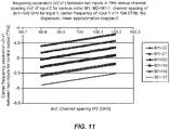
- Taking Δv 1 equal to 100 GHz, v 1 =194.0THz, it is shown in
Fig. 11 how for various orders M1, M2=M1-1, the channel spacing ofinput 2 is also very close to 100Ghz, within the range 99.8 to 100.2GHz as desired. This holds for a wide range of frequency separations between the two inputs. - In
Fig. 12 , the channel spacing for both inputs is kept exactly Δv 1 = Δv 2 =100.0 GHz and it is shown again how arbitrary frequency separation between the two inputs can be achieved, now by simply varying the frequency v 1 ofinput 1 and the output under consideration. - The dual input AWG techniques described herein need not be used only for implementing the ITU grid frequencies. In order to demonstrate this,
Fig. 13 reproduces the technology specific channel plans mentioned earlier and as shown in the table ofFig. 2 . Here an arbitrary frequency separation can be created with channel spacing of Δv 1 =100 GHz forinput 1, and Δv 2 =97.37 Ghz forinput 2. - The above examples are calculated for a situation with zero waveguide and material dispersion, α=1.0. However, arbitrary channel plans can be achieved also in the presence of waveguide and material dispersion. Using this approach, having multiple inputs operating on different order, allows one to make channel plans agnostic to the technology parameters in which the AWGs are fabricated.
- Another benefit of the multi-input AWGs here described over a single input cyclic AWG is that the two inputs can each have empirical corrections. For example by UV-writing prisms in the path of each beam (triangular regions of different index) or moving one input relative to the other(s) by other means.
- The model equation gives solutions for M1 and M2, v 1 and v 2, etc. In order to calculate the input and output angles one should use the grating equation, or deflection equation for each of the inputs

input 1, and M2 forinput 2, and so on for cases of more than 2 inputs. - A typical design process, knowing the various indices of refraction and desired center frequencies and channel spacings for each of the inputs, might proceed as follows.
- First, using eq.4 (or a simplification thereof), select orders M1 and M2=M1-1 that best satisfy the desired values. This may be most easily accomplished by preparing charts such as
Fig. 11 and12 , and selecting the orders whose plot best satisfies the desired values. Some tradeoffs may be necessary in the precision of either channel spacing or frequency spacing or both, as previously explained, but the resulting design can approximate the desired values very closely. - Next, select an input angle for IP1 and select any output angle, such as 0 radians. Given this information, together with the frequencies and the orders just selected, the grating equation is used to determine the length increment ΔL between adjacent waveguides in the array.
- Next, now that the orders M1 and M2 and ΔL are known, the equation above relating sin θ IP2 to sin θ IP1 and ΔL is used to calculate the required angular spacing between the inputs.
- Next, the grating equation is used to calculate the required angles for all the output receivers. This calculation can be done for either of the inputs since both should yield the same angles for the output receivers.
- Finally, empirical adjustments can be made as previously described.
- It has already been mentioned that because the orders addressed by the inputs to the AWG must be integers, the equations and techniques described herein may not achieve desired channel plans and frequency separations exactly, though they can be made extremely close. Some examples described herein for example achieve a channel spacing which deviates by no more than 2GHz from a desired 100GHz channel spacing. If a device is made according to the equations and techniques described herein, it is still considered to achieve the desired channel plans and frequency separations "substantially".
- Additionally, in a real device making use of the concepts described herein, it will be appreciated that it may be either impossible or commercially unnecessary to match the equations set forth above exactly. For example, the devices may deviate from the equations due to ordinary manufacturing tolerances. A real device which deviates from the equations set forth above for any of these reasons, is considered herein still to satisfy the equations "substantially". Since such devices still make use of the novel concepts taught herein they can be made with much better accuracy than conventional devices, even though they do not satisfy the equations exactly. Furthermore, whereas virtually any desired channel plan and frequency separation can be achieved using the equations and techniques described herein, it will be appreciated that an embodiment can still come closer to desired channel plans and frequency separations than can conventional devices and techniques, if the equations and techniques described herein are used with a small spoiling factor. Embodiments such as this are still considered herein to take advantage of the equations and techniques described herein and are therefore still considered to satisfy the equations "substantially".
- The applicant hereby discloses in isolation each individual feature described herein and any combination of two or more such features, to the extent that such features or combinations are capable of being carried out based on the present specification as a whole in light of the common general knowledge of a person skilled in the art, irrespective of whether such features or combinations of features solve any problems disclosed herein, and without limitation to the scope of the claims. The applicant indicates that aspects of the present invention may consist of any such feature or combination of features. In view of the foregoing description it will be evident to a person skilled in the art that various modifications may be made within the scope of the invention.
- The foregoing description of preferred embodiments of the present invention has been provided for the purposes of illustration and description. It is not intended to be exhaustive or to limit the invention to the precise forms disclosed. Obviously, many modifications and variations will be apparent to practitioners skilled in this art. In particular, and without limitation, any and all variations described, suggested or incorporated by reference in the Background section of this patent application are specifically incorporated by reference into the description herein of embodiments of the invention. In addition, any and all variations described, suggested or incorporated by reference herein with respect to any one embodiment are also to be considered taught with respect to all other embodiments. The embodiments described herein were chosen and described in order to best explain the principles of the invention and its practical application, thereby enabling others skilled in the art to understand the invention for various embodiments and with various modifications as are suited to the particular use contemplated. It is intended that the scope of the invention be defined by the following claims and their equivalents.
Claims (18)
- Arrayed waveguide grating apparatus comprising an input free-space region, an output free-space region, and an array of waveguides from the input free-space region to the output free-space region, the output free space region having a far boundary disposed across the output free space region from the array,
wherein the input free-space region has an input port comprising at least first and second inputs, the first input being for carrying optical energy according to a first channel plan identifying a first center frequency and a first plurality of wavelength channels with a first constant channel spacing, and the second input being for carrying optical energy according to a second channel plan identifying a second center frequency and a second plurality of wavelength channels with a second constant channel spacing, the first and second center frequencies being different,
wherein the first input is disposed such that optical energy according to the first channel plan provided on the first input will, using a first order M1 of the waveguide array, image first, second and third adjacent channels of the optical energy according to the first channel plan on the far boundary at respective angles θ OP1, θ OP2 and θ OP3 measured relative to where the array centerline meets the output free-space region,
and wherein the second input is disposed such that optical energy according to the second channel plan provided on the second input will, using a second order M2 of the waveguide array different from the first order M1, image first, second and third adjacent channels of the optical energy according to the second channel plan on the far boundary at the respective angles θ OP1, θ OP2 and θ OP3, at least one of the first, second and third channels in the second channel plan having a wavelength that differ from all of the first, second and third channels in the first channel plan. - Apparatus according to claim 1, wherein the first and second inputs are disposed across the input free-space region from the array at angles θ IP1 and θ IP2 measured relative to where the array centerline meets the input free-space region,
where θ IP1 and θ IP2 substantially satisfy
where v2N2 is the second center frequency, Δ(v2N2) being the second channel spacing,
where da is a pitch of the array waveguides where they meet the input free space region, where c is the speed of light in a vacuum,
and where Ns1 is the effective index of refraction in the input free space region at frequency v1, Ns2 is the effective index of refraction in the input free space region at frequency v2, N1 is the effective index of refraction of a waveguide in the waveguide array at frequency v1, N2 is the effective index of refraction of a waveguide in the waveguide array at frequency v2,
and where Δ(v1N1)/Δ(v2N2) substantially satisfies

- Apparatus according to any preceding claim, wherein the first and second center frequencies are in different ones of the O-band, E-band, S-band, C-band, L-band and U-band.
- Apparatus according to any preceding claim, wherein the first and second center frequencies are in respectively the C-band and L-band.
- Apparatus according to claim 1 or 2, wherein the first and second center frequencies are in two different sub-bands of a single one of the O-band, E-band, S-band, C-band, L-band and U-band.
- Apparatus according to any preceding claim, wherein the first and second orders are related as M2 = M1-1.
- Apparatus according to any preceding claim, wherein the first and second channel spacings are substantially equal.
- Apparatus according to any preceding claim, wherein the first and second channel spacings are both equal to 50GHz and the first and second center frequencies both lie substantially on multiples of 50GHz.
- Apparatus according to any of claims 1-7, wherein the first and second channel spacings are both substantially equal to 50GHz and the first and second center frequencies both lie on multiples of 50GHz.
- Apparatus according to any of claims 1-7, wherein the first and second channel spacings are both substantially equal to 50GHz and the first and second center frequencies both lie substantially on multiples of 50GHz.
- A method for operating an AWG having first and second inputs, a plurality of outputs, an input free-space region, an output free-space region, and an array of waveguides from the input free-space region to the output free-space region, the output free space region having a far boundary disposed across the output free space region from the array, the first and second inputs being addressed to respective first and second different orders of the AWG, said method comprising the steps of:simultaneously providing optical energy according to a first channel plan into the first input and optical energy according to a second channel plan into the second input, the first channel plan identifying a first center frequency and a first plurality of wavelength channels with a first constant channel spacing, and the second channel plan identifying a second center frequency and a second plurality of wavelength channels with a second constant channel spacing, the first and second center frequencies being different,using a first order M1 of the waveguide array to image first, second and third adjacent channels of the optical energy of the first channel plan on the far boundary at respective angles θ OP1, θ OP2 and θ OP3 measured relative to where the array centerline meets the output free-space region, andusing a second order M2 of the waveguide array different from the first order M1, to image first, second and third adjacent channels of the optical energy of the second channel plan on the far boundary at respective angles θ OP1, θ OP2 and θ OP3,wherein at least one of the first, second and third channels in the second channel plan has a wavelength that differs from all of the first, second and third channels in the first channel plan.
- A system comprising a first AWG having a plurality of inputs and at least first and second outputs and a second AWG formed in accordance with any of claims 1-10, for use with a transmission path carrying first optical energy from the first output of the first AWG to the first input of the second AWG and from the second output of the first AWG to the second input of the second AWG,
wherein the first and second outputs of the first AWG address respectively first and second different orders of the first AWG such that optical energy carried on the first output of the first AWG has a plurality of channels conforming to the first channel plan and at the same time optical energy carried on the second output of the first AWG has a plurality of channels conforming to the second channel plan. - A system according to claim 12, wherein the first and second AWGs are fabricated with different sets of technology parameters.
- A system according to claim 12 or 13, further comprising the transmission path, wherein the transmission path comprises a first optical fiber carrying the first optical energy and a second optical fiber carrying the second optical energy.
- A system according to claim 12 or 13, wherein the transmission path comprises a single optical fiber, further comprising:a first WDM filter/combiner having two inputs in optical communication with respectively the first and second outputs of the first AWG and an output in communication with a first end of the single optical fiber; anda second WDM filter/combiner having one input in communication with a second end of the single optical fiber and two outputs in optical communication with respectively the first and second inputs of the second AWG.
- A system according to claim 15, further comprising the transmission path.
- Apparatus according to any of claims 1-10, wherein the output free-space region has an output port comprising a plurality of outputs, including first, second and third outputs disposed on the far boundary at the respective angles θ OP1, θ OP2 and θ OP3.
- Apparatus according to claim 1 or 2, wherein the first constant channel spacing is a constant frequency channel spacing.
Applications Claiming Priority (3)
| Application Number | Priority Date | Filing Date | Title |
|---|---|---|---|
| US39213110P | 2010-10-12 | 2010-10-12 | |
| US13/271,886 US9494735B2 (en) | 2010-10-12 | 2011-10-12 | AWG supporting multiple frequency bands and channel plans through respective multiple inputs |
| PCT/US2011/055982 WO2012051314A2 (en) | 2010-10-12 | 2011-10-12 | Awg supporting multiple frequency bands and channel plans |
Publications (3)
| Publication Number | Publication Date |
|---|---|
| EP2628037A2 EP2628037A2 (en) | 2013-08-21 |
| EP2628037A4 EP2628037A4 (en) | 2015-03-04 |
| EP2628037B1 true EP2628037B1 (en) | 2018-05-23 |
Family
ID=45925229
Family Applications (1)
| Application Number | Title | Priority Date | Filing Date |
|---|---|---|---|
| EP11833344.2A Active EP2628037B1 (en) | 2010-10-12 | 2011-10-12 | Awg supporting multiple frequency bands and channel plans |
Country Status (3)
| Country | Link |
|---|---|
| US (1) | US9494735B2 (en) |
| EP (1) | EP2628037B1 (en) |
| WO (1) | WO2012051314A2 (en) |
Families Citing this family (10)
| Publication number | Priority date | Publication date | Assignee | Title |
|---|---|---|---|---|
| EP2628037B1 (en) * | 2010-10-12 | 2018-05-23 | Gemfire Corporation | Awg supporting multiple frequency bands and channel plans |
| US8565600B2 (en) * | 2011-06-10 | 2013-10-22 | Neophotonics Corporation | Optical network configurations with multiple band multiplexing and de-multiplexing and AWG structures with multiple band processing |
| US9002214B2 (en) | 2011-07-14 | 2015-04-07 | Applied Optoelectronics, Inc. | Wavelength-selectable laser device and apparatus and system including same |
| US9502858B2 (en) | 2011-07-14 | 2016-11-22 | Applied Optoelectronics, Inc. | Laser array mux assembly with external reflector for providing a selected wavelength or multiplexed wavelengths |
| US9172491B2 (en) * | 2012-01-30 | 2015-10-27 | Aeponyx Inc. | Method, topology and point of presence equipment for serving a plurality of users via a multiplex module |
| US9214790B2 (en) * | 2012-10-03 | 2015-12-15 | Applied Optoelectronics, Inc. | Filtered laser array assembly with external optical modulation and WDM optical system including same |
| US9025958B1 (en) | 2013-09-03 | 2015-05-05 | Avago Technologies General Ip (Singapore) Pte. Ltd. | Planar lightwave circuit optical multiplexer for non-sequential wavelength channels |
| WO2018123921A1 (en) * | 2016-12-28 | 2018-07-05 | 日本電信電話株式会社 | Optical signal processing device |
| CN110196467A (en) * | 2019-06-14 | 2019-09-03 | 武汉光迅科技股份有限公司 | A kind of multi input type array waveguide grating and preparation method thereof |
| CN114915340B (en) * | 2021-02-09 | 2023-08-04 | 讯芸电子科技(中山)有限公司 | Optical communication module |
Family Cites Families (15)
| Publication number | Priority date | Publication date | Assignee | Title |
|---|---|---|---|---|
| US5002350A (en) | 1990-02-26 | 1991-03-26 | At&T Bell Laboratories | Optical multiplexer/demultiplexer |
| FR2742882B1 (en) | 1995-12-22 | 1998-02-13 | Corning Inc | WAVELENGTH DEMULTIPLEXER, MADE IN INTEGRATED OPTICS |
| FR2753803B1 (en) * | 1996-09-24 | 1998-12-11 | MULTIPLEXER COMPONENT WITH SPECTROGRAPH WITH WAVEGUID ARRAY | |
| US6181849B1 (en) | 1999-04-30 | 2001-01-30 | Lucent Technologies, Inc. | Interleaved wavelengths multi/demultiplexer with multiple-input-ports and multiple-output-ports for wavelength add/drop WDM systems |
| CA2328696C (en) | 2000-12-18 | 2008-08-12 | Jds Uniphase Inc. | Periodic arrayed waveguide grating multiplexer/demultiplexer |
| US6678446B1 (en) * | 2001-10-03 | 2004-01-13 | Lightwave Microsystems Corporation | Multi-band arrayed waveguide grating |
| US6956993B2 (en) | 2003-06-27 | 2005-10-18 | Lucent Technologies Inc. | Arrayed waveguide gratings with improved transmission efficiency |
| KR100594040B1 (en) | 2004-01-08 | 2006-06-30 | 삼성전자주식회사 | Dual-band wavelength division multiplexer |
| US7397986B2 (en) | 2005-03-04 | 2008-07-08 | Gemfire Corporation | Optical device with reduced temperature dependence |
| KR100742651B1 (en) | 2005-08-31 | 2007-07-25 | 노베라옵틱스코리아 주식회사 | Multiple branch wdm-pon system using cyclic awg |
| US7440655B2 (en) * | 2005-09-21 | 2008-10-21 | Andevices, Inc. | Duplex arrayed waveguide grating |
| US7492991B2 (en) | 2006-04-28 | 2009-02-17 | Gemfire Corporation | Arrayed waveguide grating with reduced channel passband asymmetry |
| CN102388329A (en) | 2009-02-26 | 2012-03-21 | 艾迪株式会社 | Arrayed waveguide grating (AWG) with different radii in the input and output slab regions |
| US8285144B2 (en) * | 2009-07-30 | 2012-10-09 | Jds Uniphase Corporation | Optical device for rearranging wavelength channels |
| EP2628037B1 (en) * | 2010-10-12 | 2018-05-23 | Gemfire Corporation | Awg supporting multiple frequency bands and channel plans |
-
2011
- 2011-10-12 EP EP11833344.2A patent/EP2628037B1/en active Active
- 2011-10-12 US US13/271,886 patent/US9494735B2/en active Active
- 2011-10-12 WO PCT/US2011/055982 patent/WO2012051314A2/en active Application Filing
Non-Patent Citations (1)
| Title |
|---|
| None * |
Also Published As
| Publication number | Publication date |
|---|---|
| WO2012051314A2 (en) | 2012-04-19 |
| US20120087667A1 (en) | 2012-04-12 |
| WO2012051314A3 (en) | 2012-07-19 |
| US9494735B2 (en) | 2016-11-15 |
| EP2628037A4 (en) | 2015-03-04 |
| EP2628037A2 (en) | 2013-08-21 |
Similar Documents
| Publication | Publication Date | Title |
|---|---|---|
| EP2628037B1 (en) | Awg supporting multiple frequency bands and channel plans | |
| US7440655B2 (en) | Duplex arrayed waveguide grating | |
| EP1226461B1 (en) | Phasar with flattened pass-band | |
| EP2776876B1 (en) | Wavelength router for a passive optical network | |
| US6959129B2 (en) | Bidirectional multiplexer and demultiplexer based on a single echelle waveguide grating | |
| US6181849B1 (en) | Interleaved wavelengths multi/demultiplexer with multiple-input-ports and multiple-output-ports for wavelength add/drop WDM systems | |
| JPH06102430A (en) | Optical device | |
| US7174071B2 (en) | Arrayed waveguide grating with increased uniformity of a performance parameter | |
| US20080044122A1 (en) | Asymmetric Mach-Zehnder Interferometer Having A Reduced Drive Voltage Coupled To A Compact Low-Loss Arrayed Waveguide Grating | |
| US6512864B1 (en) | Optical multiplexer/demultiplexer arrangement for WDM signals having in-band and out-of-band signal components | |
| US6266460B1 (en) | Large-channel-count programmable wavelength add-drop | |
| KR20140100565A (en) | Arrayed waveguide grating, optical module providied with said arryed waveguide, and optical communications system | |
| KR20020055445A (en) | Arrayed waveguide grating type otpical multiplexer/demultiplexer | |
| US20050141813A1 (en) | Arrayed waveguide wavelength multiplexing apparatus and optical transmitter | |
| WO2000034811A1 (en) | Arrayed waveguide grating multiplexer and demultiplexer | |
| Doerr et al. | Planar lightwave circuit eight-channel CWDM multiplexer with< 3.9-dB insertion loss | |
| US20020176660A1 (en) | Optical wavelength multiplexer/demultiplexer and use method thereof | |
| US20030128926A1 (en) | Compact wavelength routing device having substantially flat passband | |
| US6956993B2 (en) | Arrayed waveguide gratings with improved transmission efficiency | |
| US20040101243A1 (en) | Wavelength division multiplexer/demultiplexer | |
| US20020164116A1 (en) | Arrayed waveguide grating type optical multiplexer/demultiplexer and optical waveguide circuit | |
| US6728447B2 (en) | Optical multiplexer/demultiplexer | |
| JP2003315570A (en) | Optical wavelength multiplexer/demultiplexer | |
| US6888980B2 (en) | Methods and techniques for achieving flattened and broadened pass band spectrum for free-space grating-based dense wavelength division multiplexers/demultiplexers | |
| Doerr et al. | Planar lightwave circuit eight-channel CWDM multiplexer |
Legal Events
| Date | Code | Title | Description |
|---|---|---|---|
| PUAI | Public reference made under article 153(3) epc to a published international application that has entered the european phase |
Free format text: ORIGINAL CODE: 0009012 |
|
| 17P | Request for examination filed |
Effective date: 20130510 |
|
| AK | Designated contracting states |
Kind code of ref document: A2 Designated state(s): AL AT BE BG CH CY CZ DE DK EE ES FI FR GB GR HR HU IE IS IT LI LT LU LV MC MK MT NL NO PL PT RO RS SE SI SK SM TR |
|
| DAX | Request for extension of the european patent (deleted) | ||
| A4 | Supplementary search report drawn up and despatched |
Effective date: 20150204 |
|
| RIC1 | Information provided on ipc code assigned before grant |
Ipc: G02B 6/12 20060101ALI20150129BHEP Ipc: G02B 6/28 20060101AFI20150129BHEP Ipc: H04J 14/02 20060101ALI20150129BHEP |
|
| 17Q | First examination report despatched |
Effective date: 20160601 |
|
| GRAP | Despatch of communication of intention to grant a patent |
Free format text: ORIGINAL CODE: EPIDOSNIGR1 |
|
| STAA | Information on the status of an ep patent application or granted ep patent |
Free format text: STATUS: GRANT OF PATENT IS INTENDED |
|
| INTG | Intention to grant announced |
Effective date: 20170622 |
|
| GRAS | Grant fee paid |
Free format text: ORIGINAL CODE: EPIDOSNIGR3 |
|
| RAP1 | Party data changed (applicant data changed or rights of an application transferred) |
Owner name: GEMFIRE CORPORATION |
|
| GRAA | (expected) grant |
Free format text: ORIGINAL CODE: 0009210 |
|
| STAA | Information on the status of an ep patent application or granted ep patent |
Free format text: STATUS: THE PATENT HAS BEEN GRANTED |
|
| AK | Designated contracting states |
Kind code of ref document: B1 Designated state(s): AL AT BE BG CH CY CZ DE DK EE ES FI FR GB GR HR HU IE IS IT LI LT LU LV MC MK MT NL NO PL PT RO RS SE SI SK SM TR |
|
| REG | Reference to a national code |
Ref country code: GB Ref legal event code: FG4D |
|
| REG | Reference to a national code |
Ref country code: CH Ref legal event code: EP |
|
| REG | Reference to a national code |
Ref country code: IE Ref legal event code: FG4D |
|
| REG | Reference to a national code |
Ref country code: DE Ref legal event code: R096 Ref document number: 602011048658 Country of ref document: DE |
|
| REG | Reference to a national code |
Ref country code: AT Ref legal event code: REF Ref document number: 1001963 Country of ref document: AT Kind code of ref document: T Effective date: 20180615 |
|
| REG | Reference to a national code |
Ref country code: NL Ref legal event code: MP Effective date: 20180523 |
|
| REG | Reference to a national code |
Ref country code: LT Ref legal event code: MG4D |
|
| REG | Reference to a national code |
Ref country code: FR Ref legal event code: PLFP Year of fee payment: 8 |
|
| PG25 | Lapsed in a contracting state [announced via postgrant information from national office to epo] |
Ref country code: FI Free format text: LAPSE BECAUSE OF FAILURE TO SUBMIT A TRANSLATION OF THE DESCRIPTION OR TO PAY THE FEE WITHIN THE PRESCRIBED TIME-LIMIT Effective date: 20180523 Ref country code: BG Free format text: LAPSE BECAUSE OF FAILURE TO SUBMIT A TRANSLATION OF THE DESCRIPTION OR TO PAY THE FEE WITHIN THE PRESCRIBED TIME-LIMIT Effective date: 20180823 Ref country code: LT Free format text: LAPSE BECAUSE OF FAILURE TO SUBMIT A TRANSLATION OF THE DESCRIPTION OR TO PAY THE FEE WITHIN THE PRESCRIBED TIME-LIMIT Effective date: 20180523 Ref country code: ES Free format text: LAPSE BECAUSE OF FAILURE TO SUBMIT A TRANSLATION OF THE DESCRIPTION OR TO PAY THE FEE WITHIN THE PRESCRIBED TIME-LIMIT Effective date: 20180523 Ref country code: SE Free format text: LAPSE BECAUSE OF FAILURE TO SUBMIT A TRANSLATION OF THE DESCRIPTION OR TO PAY THE FEE WITHIN THE PRESCRIBED TIME-LIMIT Effective date: 20180523 Ref country code: NO Free format text: LAPSE BECAUSE OF FAILURE TO SUBMIT A TRANSLATION OF THE DESCRIPTION OR TO PAY THE FEE WITHIN THE PRESCRIBED TIME-LIMIT Effective date: 20180823 |
|
| PG25 | Lapsed in a contracting state [announced via postgrant information from national office to epo] |
Ref country code: HR Free format text: LAPSE BECAUSE OF FAILURE TO SUBMIT A TRANSLATION OF THE DESCRIPTION OR TO PAY THE FEE WITHIN THE PRESCRIBED TIME-LIMIT Effective date: 20180523 Ref country code: LV Free format text: LAPSE BECAUSE OF FAILURE TO SUBMIT A TRANSLATION OF THE DESCRIPTION OR TO PAY THE FEE WITHIN THE PRESCRIBED TIME-LIMIT Effective date: 20180523 Ref country code: GR Free format text: LAPSE BECAUSE OF FAILURE TO SUBMIT A TRANSLATION OF THE DESCRIPTION OR TO PAY THE FEE WITHIN THE PRESCRIBED TIME-LIMIT Effective date: 20180824 Ref country code: RS Free format text: LAPSE BECAUSE OF FAILURE TO SUBMIT A TRANSLATION OF THE DESCRIPTION OR TO PAY THE FEE WITHIN THE PRESCRIBED TIME-LIMIT Effective date: 20180523 Ref country code: NL Free format text: LAPSE BECAUSE OF FAILURE TO SUBMIT A TRANSLATION OF THE DESCRIPTION OR TO PAY THE FEE WITHIN THE PRESCRIBED TIME-LIMIT Effective date: 20180523 |
|
| REG | Reference to a national code |
Ref country code: AT Ref legal event code: MK05 Ref document number: 1001963 Country of ref document: AT Kind code of ref document: T Effective date: 20180523 |
|
| PG25 | Lapsed in a contracting state [announced via postgrant information from national office to epo] |
Ref country code: AT Free format text: LAPSE BECAUSE OF FAILURE TO SUBMIT A TRANSLATION OF THE DESCRIPTION OR TO PAY THE FEE WITHIN THE PRESCRIBED TIME-LIMIT Effective date: 20180523 Ref country code: PL Free format text: LAPSE BECAUSE OF FAILURE TO SUBMIT A TRANSLATION OF THE DESCRIPTION OR TO PAY THE FEE WITHIN THE PRESCRIBED TIME-LIMIT Effective date: 20180523 Ref country code: CZ Free format text: LAPSE BECAUSE OF FAILURE TO SUBMIT A TRANSLATION OF THE DESCRIPTION OR TO PAY THE FEE WITHIN THE PRESCRIBED TIME-LIMIT Effective date: 20180523 Ref country code: SK Free format text: LAPSE BECAUSE OF FAILURE TO SUBMIT A TRANSLATION OF THE DESCRIPTION OR TO PAY THE FEE WITHIN THE PRESCRIBED TIME-LIMIT Effective date: 20180523 Ref country code: RO Free format text: LAPSE BECAUSE OF FAILURE TO SUBMIT A TRANSLATION OF THE DESCRIPTION OR TO PAY THE FEE WITHIN THE PRESCRIBED TIME-LIMIT Effective date: 20180523 Ref country code: EE Free format text: LAPSE BECAUSE OF FAILURE TO SUBMIT A TRANSLATION OF THE DESCRIPTION OR TO PAY THE FEE WITHIN THE PRESCRIBED TIME-LIMIT Effective date: 20180523 Ref country code: DK Free format text: LAPSE BECAUSE OF FAILURE TO SUBMIT A TRANSLATION OF THE DESCRIPTION OR TO PAY THE FEE WITHIN THE PRESCRIBED TIME-LIMIT Effective date: 20180523 |
|
| PGFP | Annual fee paid to national office [announced via postgrant information from national office to epo] |
Ref country code: DE Payment date: 20181029 Year of fee payment: 8 |
|
| REG | Reference to a national code |
Ref country code: DE Ref legal event code: R097 Ref document number: 602011048658 Country of ref document: DE |
|
| PG25 | Lapsed in a contracting state [announced via postgrant information from national office to epo] |
Ref country code: SM Free format text: LAPSE BECAUSE OF FAILURE TO SUBMIT A TRANSLATION OF THE DESCRIPTION OR TO PAY THE FEE WITHIN THE PRESCRIBED TIME-LIMIT Effective date: 20180523 Ref country code: IT Free format text: LAPSE BECAUSE OF FAILURE TO SUBMIT A TRANSLATION OF THE DESCRIPTION OR TO PAY THE FEE WITHIN THE PRESCRIBED TIME-LIMIT Effective date: 20180523 |
|
| PGFP | Annual fee paid to national office [announced via postgrant information from national office to epo] |
Ref country code: FR Payment date: 20181025 Year of fee payment: 8 |
|
| PLBE | No opposition filed within time limit |
Free format text: ORIGINAL CODE: 0009261 |
|
| STAA | Information on the status of an ep patent application or granted ep patent |
Free format text: STATUS: NO OPPOSITION FILED WITHIN TIME LIMIT |
|
| 26N | No opposition filed |
Effective date: 20190226 |
|
| PG25 | Lapsed in a contracting state [announced via postgrant information from national office to epo] |
Ref country code: SI Free format text: LAPSE BECAUSE OF FAILURE TO SUBMIT A TRANSLATION OF THE DESCRIPTION OR TO PAY THE FEE WITHIN THE PRESCRIBED TIME-LIMIT Effective date: 20180523 |
|
| REG | Reference to a national code |
Ref country code: CH Ref legal event code: PL |
|
| REG | Reference to a national code |
Ref country code: BE Ref legal event code: MM Effective date: 20181031 |
|
| PG25 | Lapsed in a contracting state [announced via postgrant information from national office to epo] |
Ref country code: LU Free format text: LAPSE BECAUSE OF NON-PAYMENT OF DUE FEES Effective date: 20181012 Ref country code: MC Free format text: LAPSE BECAUSE OF FAILURE TO SUBMIT A TRANSLATION OF THE DESCRIPTION OR TO PAY THE FEE WITHIN THE PRESCRIBED TIME-LIMIT Effective date: 20180523 |
|
| REG | Reference to a national code |
Ref country code: IE Ref legal event code: MM4A |
|
| REG | Reference to a national code |
Ref country code: GB Ref legal event code: 732E Free format text: REGISTERED BETWEEN 20190711 AND 20190717 |
|
| PG25 | Lapsed in a contracting state [announced via postgrant information from national office to epo] |
Ref country code: CH Free format text: LAPSE BECAUSE OF NON-PAYMENT OF DUE FEES Effective date: 20181031 Ref country code: BE Free format text: LAPSE BECAUSE OF NON-PAYMENT OF DUE FEES Effective date: 20181031 Ref country code: LI Free format text: LAPSE BECAUSE OF NON-PAYMENT OF DUE FEES Effective date: 20181031 |
|
| PG25 | Lapsed in a contracting state [announced via postgrant information from national office to epo] |
Ref country code: IE Free format text: LAPSE BECAUSE OF NON-PAYMENT OF DUE FEES Effective date: 20181012 |
|
| PG25 | Lapsed in a contracting state [announced via postgrant information from national office to epo] |
Ref country code: AL Free format text: LAPSE BECAUSE OF FAILURE TO SUBMIT A TRANSLATION OF THE DESCRIPTION OR TO PAY THE FEE WITHIN THE PRESCRIBED TIME-LIMIT Effective date: 20180523 |
|
| PG25 | Lapsed in a contracting state [announced via postgrant information from national office to epo] |
Ref country code: MT Free format text: LAPSE BECAUSE OF NON-PAYMENT OF DUE FEES Effective date: 20181012 |
|
| PG25 | Lapsed in a contracting state [announced via postgrant information from national office to epo] |
Ref country code: TR Free format text: LAPSE BECAUSE OF FAILURE TO SUBMIT A TRANSLATION OF THE DESCRIPTION OR TO PAY THE FEE WITHIN THE PRESCRIBED TIME-LIMIT Effective date: 20180523 |
|
| REG | Reference to a national code |
Ref country code: DE Ref legal event code: R119 Ref document number: 602011048658 Country of ref document: DE |
|
| PG25 | Lapsed in a contracting state [announced via postgrant information from national office to epo] |
Ref country code: PT Free format text: LAPSE BECAUSE OF FAILURE TO SUBMIT A TRANSLATION OF THE DESCRIPTION OR TO PAY THE FEE WITHIN THE PRESCRIBED TIME-LIMIT Effective date: 20180523 |
|
| PG25 | Lapsed in a contracting state [announced via postgrant information from national office to epo] |
Ref country code: HU Free format text: LAPSE BECAUSE OF FAILURE TO SUBMIT A TRANSLATION OF THE DESCRIPTION OR TO PAY THE FEE WITHIN THE PRESCRIBED TIME-LIMIT; INVALID AB INITIO Effective date: 20111012 Ref country code: CY Free format text: LAPSE BECAUSE OF FAILURE TO SUBMIT A TRANSLATION OF THE DESCRIPTION OR TO PAY THE FEE WITHIN THE PRESCRIBED TIME-LIMIT Effective date: 20180523 Ref country code: MK Free format text: LAPSE BECAUSE OF NON-PAYMENT OF DUE FEES Effective date: 20180523 |
|
| PG25 | Lapsed in a contracting state [announced via postgrant information from national office to epo] |
Ref country code: DE Free format text: LAPSE BECAUSE OF NON-PAYMENT OF DUE FEES Effective date: 20200501 Ref country code: IS Free format text: LAPSE BECAUSE OF FAILURE TO SUBMIT A TRANSLATION OF THE DESCRIPTION OR TO PAY THE FEE WITHIN THE PRESCRIBED TIME-LIMIT Effective date: 20180923 |
|
| PG25 | Lapsed in a contracting state [announced via postgrant information from national office to epo] |
Ref country code: FR Free format text: LAPSE BECAUSE OF NON-PAYMENT OF DUE FEES Effective date: 20191031 |
|
| PGFP | Annual fee paid to national office [announced via postgrant information from national office to epo] |
Ref country code: GB Payment date: 20231018 Year of fee payment: 13 |