EP2626908A1 - Solar cell element and method for manufacturing same - Google Patents
Solar cell element and method for manufacturing same Download PDFInfo
- Publication number
- EP2626908A1 EP2626908A1 EP11830651.3A EP11830651A EP2626908A1 EP 2626908 A1 EP2626908 A1 EP 2626908A1 EP 11830651 A EP11830651 A EP 11830651A EP 2626908 A1 EP2626908 A1 EP 2626908A1
- Authority
- EP
- European Patent Office
- Prior art keywords
- semiconductor substrate
- solar cell
- cell element
- antireflection film
- tellurium
- Prior art date
- Legal status (The legal status is an assumption and is not a legal conclusion. Google has not performed a legal analysis and makes no representation as to the accuracy of the status listed.)
- Granted
Links
Images

Classifications
-
- H—ELECTRICITY
- H10—SEMICONDUCTOR DEVICES; ELECTRIC SOLID-STATE DEVICES NOT OTHERWISE PROVIDED FOR
- H10F—INORGANIC SEMICONDUCTOR DEVICES SENSITIVE TO INFRARED RADIATION, LIGHT, ELECTROMAGNETIC RADIATION OF SHORTER WAVELENGTH OR CORPUSCULAR RADIATION
- H10F10/00—Individual photovoltaic cells, e.g. solar cells
-
- H—ELECTRICITY
- H10—SEMICONDUCTOR DEVICES; ELECTRIC SOLID-STATE DEVICES NOT OTHERWISE PROVIDED FOR
- H10F—INORGANIC SEMICONDUCTOR DEVICES SENSITIVE TO INFRARED RADIATION, LIGHT, ELECTROMAGNETIC RADIATION OF SHORTER WAVELENGTH OR CORPUSCULAR RADIATION
- H10F77/00—Constructional details of devices covered by this subclass
- H10F77/20—Electrodes
- H10F77/206—Electrodes for devices having potential barriers
- H10F77/211—Electrodes for devices having potential barriers for photovoltaic cells
-
- H—ELECTRICITY
- H01—ELECTRIC ELEMENTS
- H01B—CABLES; CONDUCTORS; INSULATORS; SELECTION OF MATERIALS FOR THEIR CONDUCTIVE, INSULATING OR DIELECTRIC PROPERTIES
- H01B1/00—Conductors or conductive bodies characterised by the conductive materials; Selection of materials as conductors
- H01B1/20—Conductive material dispersed in non-conductive organic material
- H01B1/22—Conductive material dispersed in non-conductive organic material the conductive material comprising metals or alloys
-
- H—ELECTRICITY
- H10—SEMICONDUCTOR DEVICES; ELECTRIC SOLID-STATE DEVICES NOT OTHERWISE PROVIDED FOR
- H10D—INORGANIC ELECTRIC SEMICONDUCTOR DEVICES
- H10D62/00—Semiconductor bodies, or regions thereof, of devices having potential barriers
- H10D62/10—Shapes, relative sizes or dispositions of the regions of the semiconductor bodies; Shapes of the semiconductor bodies
- H10D62/117—Shapes of semiconductor bodies
-
- H—ELECTRICITY
- H10—SEMICONDUCTOR DEVICES; ELECTRIC SOLID-STATE DEVICES NOT OTHERWISE PROVIDED FOR
- H10F—INORGANIC SEMICONDUCTOR DEVICES SENSITIVE TO INFRARED RADIATION, LIGHT, ELECTROMAGNETIC RADIATION OF SHORTER WAVELENGTH OR CORPUSCULAR RADIATION
- H10F71/00—Manufacture or treatment of devices covered by this subclass
-
- H—ELECTRICITY
- H10—SEMICONDUCTOR DEVICES; ELECTRIC SOLID-STATE DEVICES NOT OTHERWISE PROVIDED FOR
- H10F—INORGANIC SEMICONDUCTOR DEVICES SENSITIVE TO INFRARED RADIATION, LIGHT, ELECTROMAGNETIC RADIATION OF SHORTER WAVELENGTH OR CORPUSCULAR RADIATION
- H10F77/00—Constructional details of devices covered by this subclass
- H10F77/20—Electrodes
-
- H—ELECTRICITY
- H10—SEMICONDUCTOR DEVICES; ELECTRIC SOLID-STATE DEVICES NOT OTHERWISE PROVIDED FOR
- H10F—INORGANIC SEMICONDUCTOR DEVICES SENSITIVE TO INFRARED RADIATION, LIGHT, ELECTROMAGNETIC RADIATION OF SHORTER WAVELENGTH OR CORPUSCULAR RADIATION
- H10F77/00—Constructional details of devices covered by this subclass
- H10F77/70—Surface textures, e.g. pyramid structures
- H10F77/703—Surface textures, e.g. pyramid structures of the semiconductor bodies, e.g. textured active layers
-
- Y—GENERAL TAGGING OF NEW TECHNOLOGICAL DEVELOPMENTS; GENERAL TAGGING OF CROSS-SECTIONAL TECHNOLOGIES SPANNING OVER SEVERAL SECTIONS OF THE IPC; TECHNICAL SUBJECTS COVERED BY FORMER USPC CROSS-REFERENCE ART COLLECTIONS [XRACs] AND DIGESTS
- Y02—TECHNOLOGIES OR APPLICATIONS FOR MITIGATION OR ADAPTATION AGAINST CLIMATE CHANGE
- Y02E—REDUCTION OF GREENHOUSE GAS [GHG] EMISSIONS, RELATED TO ENERGY GENERATION, TRANSMISSION OR DISTRIBUTION
- Y02E10/00—Energy generation through renewable energy sources
- Y02E10/50—Photovoltaic [PV] energy
Definitions
- the present invention relates to a solar cell element and a method for manufacturing the same.
- a solar cell element generally has a silicon-based, for example, p-type semiconductor substrate, an n-type diffusion layer, an antireflection film, a back surface electrode, and a front surface electrode.
- a conductive paste obtained by mixing conductive particles comprising silver as a main component with glass frit, an organic vehicle, a solvent, etc. is used when forming the front surface electrode. This conductive paste is formed into an electrode pattern by screen printing, stencil printing or the like, and then fired to form the front surface electrode.
- glass having good solubility with the antireflection film be used as the glass frit of the conductive paste. So far, glass containing lead oxide often has been used due to its excellent adherence to a semiconductor substrate and because it is easy to adjust its softening point and the fire-through process can be executed relatively favorably (see Patent Document 1, for example).
- Patent Document 1 Japanese Patent Publication No. 2001-93326 A
- An object of the present invention is to provide a solar cell element in which favorable ohmic contact can be realized between a semiconductor substrate and a front surface electrode and in which fire-through can be controlled optimally, and a method for manufacturing such a solar cell element.
- a solar cell element according to one aspect of the present invention comprises:
- a method for manufacturing the solar cell element according to one aspect of the present invention is a method for manufacturing a solar cell element which comprises a semiconductor substrate, an antireflection film disposed in a first region on one main surface of the semiconductor substrate, and a front surface electrode disposed in a second region on the one main surface of the semiconductor substrate, the method comprising:
- optimal fire-through (firing-through) property can be secured by firing the conductive paste and excellent ohmic contact can be realized between the semiconductor substrate and the front surface electrode.
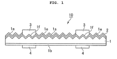
- a solar cell element 10 of the present embodiment has a semiconductor substrate 1 that has a first semiconductor region of one conductivity-type and a second semiconductor region of an opposite conductivity type (an opposite conductivity type layer 1a) opposite to that of the first semiconductor region, and an antireflection film 2 that is disposed in a first region 1e on a first surface (on the opposite conductivity type layer 1a, in the present embodiment), which is a main surface of the semiconductor substrate 1 where light enters.
- the solar cell element 10 further has a first electrode 3, which is a front surface electrode provided in a second region 1f on the first surface of the semiconductor substrate 1, and a second electrode 4, which is a back surface electrode provided on a second surface of the semiconductor substrate 1, which is a main surface on the side opposite to the first surface of the semiconductor substrate 1.
- a crystalline silicon substrate such as a monocrystalline silicon substrate or a multicrystalline silicon substrate that has a predetermined dopant element (an impurity for conductivity type control) and exhibits one conductivity type (e.g., p-type) is used as the semiconductor substrate 1.
- the thickness of the semiconductor substrate 1 is preferably, for example, equal to or less than 250 ⁇ m, and more preferably equal to or less than 150 ⁇ m.
- a case where a crystalline silicon substrate exhibiting a conductivity type of p-type is used as the semiconductor substrate 1 is described by way of example.
- boron or gallium for example, be used as the dopant element.
- a great number of microscopic projections 1c are formed on the first surface side of the semiconductor substrate 1. These microscopic projections 1c are provided in order to cause multiple reflection of light emitted onto the front surface side of the semiconductor substrate 1 and reduce the reflection of the light from the surface. These microscopic projections 1c are in the shape of a cone or a pyramid, the size of which can be changed by controlling a gas concentration or etching time in an RIE (Reactive Ion Etching) method.
- RIE Reactive Ion Etching
- the opposite conductivity type layer 1a is a layer that exhibits a conductivity type opposite to that of the semiconductor substrate 1 and is formed within a surface layer of, for example, the first surface of the semiconductor substrate 1.
- the opposite conductivity type layer 1a is formed to exhibit a conductivity type of n-type.
- the opposite conductivity type layer 1a can be formed by, for example, diffusing impurities such as phosphorus in the first surface of the silicon substrate.
- the antireflection film 2 serves to reduce the reflectance of light having a desired wavelength range and increase the amount of photogenerated carriers and is capable of improving a photocurrent density Jsc of the solar cell element 10.
- the antireflection film 2 is configured by, for example, a SiNx film, TiO 2 film, SiO 2 film, MgO film, ITO film, SnO 2 film, ZnO film, or the like.
- the thickness of the antireflection film 2 is set appropriately depending on the constituting material so as to be able to realize non-reflective conditions with respect to appropriate incident light.
- a BSF (Back Surface Field) region 1b exhibiting a conductivity type of p+ is formed in a surface layer part on the second surface side of the semiconductor substrate 1 of the solar cell element 10, as shown in Fig. 1 .
- the BSF region 1b serves to suppress the efficiency reduction caused by recombination of carriers in the vicinity of the second surface of the semiconductor substrate 1 and forms an internal electric field on the second surface side of the semiconductor substrate 1.
- the first electrode 3 has first bus bar electrodes and a plurality of linear finger electrodes intersecting with the first bus bar electrodes .
- the width of the first bus bar electrodes is approximately, for example, 1.3 to 2.5 mm.
- the finger electrodes are in a linear shape and have a width of approximately 50 to 200 ⁇ m, which is narrower than the first bus bar electrodes.
- the plurality of finger electrodes are provided at intervals of approximately 1. 5 to 3 mm therebetween.
- the thickness of the first electrodes 3 is approximately 10 to 40 ⁇ m.
- the first electrodes 3 described above can be formed by screen printing or the like a conductive paste into a desired shape and thereafter firing.
- the conductive paste used comprises a conductive powder containing silver as a main component, a tellurium-based glass frit containing tellurium, tungsten, and bismuth as essential components, and an organic vehicle, as described in detail hereinafter.
- the second electrode 4 may have the same electrode shape as the first electrodes 3 and can be formed with the same material and method as the first electrode 3 described above. Also, second bus bar electrodes comprising silver may be formed, and a collector electrode comprising aluminum may be formed on substantially the entire surface of the second surface of the semiconductor substrate 1 excluding a part of the second bus bar electrodes.
- a texture structure of the solar cell element of the present embodiment and the conductive paste used in electrode formation are described next in detail.
- the solar cell element 10 has a texture structure in which the projections 1c having average width and height of 2 ⁇ m or less are formed on the first surface side of the semiconductor substrate 1.
- the microscopic projections 1c to be formed have average width and height of 2 ⁇ m or less. Average width and height of the projections 1c greater than 2 ⁇ m need an increased etching processing time while there is no appreciable further reduction of the reflectance at the front surface of the semiconductor substrate 1.
- the average width and height of the projections 1c are not less than 0.1 ⁇ m but not more than 1 ⁇ m. This range is preferable in terms of being able to reduce the reflectance at the surface of the semiconductor substrate 1 and to improve the adherence strength to the first electrode 3.
- the average width and height of the microscopic projections 1c be not less than 0.1 ⁇ m but not more than 1 ⁇ m in order to evenly form the microscopic projections 1c over the entire first surface of the semiconductor substrate 1 with accurate controllability.
- the microscopic projections 1c have an aspect ratio (height/width of the projections 1c) of 0.1 to 2 on average.
- the aspect ratio is not more than 0.1, the average reflectance of light having a wavelength of, for example, 500 to 1000 nm is approximately 25%, increasing the reflectance at the front surface of the semiconductor substrate 1.
- an aspect ratio of not less than 2 on average breaks the microscopic projections 1c during the manufacturing process and causes more leakage current when the solar cell element 10 is formed. As a result, favorable output characteristics cannot be accomplished.
- the conductive paste for forming the first electrode 3, which is the front surface electrode, is described in detail.
- the first electrode 3 comprises silver as a main component and contains a tellurium-based glass containing tellurium, tungsten, and bismuth as essential components.
- the conductive paste for forming the first electrode 3 contains the above-described conductive powder, glass frit, appropriate additive, and organic vehicle.
- main component means a component that is contained in an amount exceeding 50 mass % and preferably a component that is contained in an amount equal to or greater than 70 mass %.
- the content of the glass frit in the conductive paste may be an amount normally contained in a conductive paste used for forming a solar cell electrode.
- the amount of glass frit be 0.1 to 10 parts by mass with respect to 100 parts by mass of conductive particles.
- the blending amount of the glass frit is equal to or greater than 0.1 parts by mass with respect to 100 parts by mass of conductive powder, predetermined adhesion and electrode strength can be obtained.
- the blending amount of the glass frit is equal to or less than 10 parts by mass with respect to 100 parts by mass of conductive powder, not only is it possible to reduce glass floating on a surface of the electrode, but also the increase in contact resistance caused by the glass flowing into an interface can be alleviated.
- the glass frit blended in the conductive paste of the present invention preferably has an average particle size of 0.5 to 5.0 ⁇ m.
- the glass frit also preferably has a softening point of 300 to 550°C.
- the organic vehicle is not particularly limited, and an organic binder, solvent, etc. commonly used as a vehicle in silver paste can be selected and mixed as appropriate.
- organic binders include celluloses, acrylic resins, phenol resins, alkyd resins, rosin esters and the like
- solvents include alcohols, ethers, esters, hydrocarbons and other organic solvents as well as water and mixed solvents of these.
- the amount of the organic vehicle is not particularly limited, and can be adjusted appropriately according to the application method or the like to an amount suitable for retaining inorganic components such as the conductive powder and the glass frit in the paste, but is normally about 5 to 40 parts by mass per 100 parts by mass of the conductive powder.
- the conductive paste used in the present invention essentially contains no lead component, and specifically the lead content of the conductive paste is 1000 ppm or less. If needed, other components such as a plasticizer, viscosity modifier, surfactant, oxidizer, metal oxide, and/or metal organic compound that are normally added as additives can appropriately be blended in the conductive paste to the extent that they do not detract from the effects of the present embodiment. In addition, silver compounds such as silver carbonate, silver oxide, and silver acetate may be blended, or copper oxide, zinc oxide, titanium oxide or the like may appropriately be added for the purpose of improving firing temperature, solar cell characteristics, and the like.
- the tellurium-based glass contains, in terms of oxide, 30 to 80 mol% of tellurium, 10 to 50 mol% of tungsten, and 5 to 25 mol% of bismuth.
- the sum of the tellurium, tungsten, and bismuth is preferably 60 mol% or more and more preferably 80 mol% or more.
- the tellurium forms a glass network as a network-former and glass formation can easily be performed as long as the content of the tellurium in the entire glass frit is 30 to 80 mol% and preferably 40 to 70 mol% in terms of oxide. This range is preferable in terms of improving fire-through characteristics.
- the tungsten contributes to expanding the vitrification range of the glass frit and stabilizing the glass frit. Glass formation can easily be performed as long as the content of the tungsten is 10 to 50 mol% and preferably 15 to 35 mol% in terms of oxide. This range is preferable in terms of further improving fire-through characteristics.
- the bismuth contributes to expanding the vitrification range of the glass frit and improving the chemical durability of the same.
- the bismuth is contained in an amount exceeding 25 mol% in terms of oxide, a crystal phase is likely to form and the stability of the glass will be impaired. It is preferred that the bismuth be contained in an amount of 5 to 25 mol% in view of lessening the problem of bleeding of the glass components.
- the glass frit described above may further contain one or more of alkali metals such as lithium and sodium, alkaline-earth metals such as magnesium, calcium, strontium, and barium, and elements such as molybdenum, zinc, aluminum, dysprosium, yttrium, niobium, lanthanum, silver, zirconium, titanium, boron, germanium, phosphorus, and tantalum.
- alkali metals such as lithium and sodium
- alkaline-earth metals such as magnesium, calcium, strontium, and barium
- elements such as molybdenum, zinc, aluminum, dysprosium, yttrium, niobium, lanthanum, silver, zirconium, titanium, boron, germanium, phosphorus, and tantalum.
- the sum of the contents of these elements is within the range of less than 40 mol% and preferably less than 20 mol%.
- the semiconductor substrate 1 is a monocrystalline silicon substrate
- the semiconductor substrate 1 is formed by, for example, a pulling method or the like.
- the semiconductor substrate 1 is a multicrystalline silicon substrate
- the semiconductor substrate 1 is formed by, for example, a casting method or the like.
- p-type multicrystalline silicon is used.
- a multicrystalline silicon ingot is prepared by, for example, a casting method.
- this ingot is sliced into a thickness of, for example, 250 ⁇ m or less.
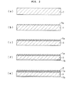
- the surface is preferably very slightly etched with an aqueous solution of, for example, NaOH or KOH or hydrofluoric acid or fluonitric acid in order to remove mechanically damaged layers of the cut section or to clean contaminated layers of the semiconductor substrate 1 (see Fig. 2(a) ).
- a great number of microscopic projections 1c are formed on the first surface side of the semiconductor substrate 1.
- These microscopic projections 1c can be formed using an RIE method. For instance, first, the semiconductor substrate 1 is installed on an upper part of an RF electrode of an RIE device, and then the inside of a chamber grounded by an earth is vacuum-drawn sufficiently using a vacuum pump. Thereafter, a predetermined flow rate of etching gas is introduced into the inside of the chamber by means of a mass flow controller, and the pressure inside the chamber is adjusted to a predetermined pressure by a pressure regulator. Thereafter, a plasma state is generated to excite and decompose the etching gas by applying RF power from an RF power supply to the RF electrode.
- the surface of the semiconductor substrate 1 is etched by the generated ions and radicals.
- Etching the surface of the semiconductor substrate 1 basically separate the constituents of the surface. However, some of the constituents cannot be separated and remain in the surface of the semiconductor substrate 1, while some of the separated substances adhere to the surface of the semiconductor substrate 1 again and become etching residues.
- the etching residues that primarily contain the materials etched from the semiconductor substrate 1 are intentionally deposited onto the surface of the semiconductor substrate 1 again and used as an etching mask, resulting in realization of roughening the surface of the semiconductor substrate 1 for forming a concave-convex structure on the surface (see Fig. 2(b) ).
- the n-type opposite conductivity type layer 1a is formed in the surface layer of the first surface of the semiconductor substrate 1.
- the opposite conductivity type layer 1a is formed by an application and thermal diffusion method for applying P 2 O 5 in a paste form to the surface of the semiconductor substrate 1 and then thermally diffusing the same, a gaseous phase thermal diffusion method for using POCl 3 (phosphorus oxychloride) in a gas form as a diffusion source, an ion implantation method for diffusing phosphorus ions directly to the surface, and the like.
- the opposite conductivity type layer 1a is formed to have a depth of approximately 0.2 to 2.0 ⁇ m and a sheet resistance of approximately 60 to 150 ⁇ / ⁇ (see Fig. 2(c) ).
- the BSF region 1b is formed on the second surface of the semiconductor substrate 1, the BSF region 1b having a semiconductor impurity of one conductivity type diffused at high concentration.
- a method for forming the BSF region 1b at a temperature of 800 to 1100°C by means of a thermal diffusion method using BBr 3 (boron tribromide) as a diffusion source and a method for applying an Al (aluminum) paste comprising Al powder, an organic vehicle and the like by means of a printing method and thereafter thermally treating (firing) the Al paste at approximately 600 to 850°C to diffuse Al on the semiconductor substrate 1.
- the method for printing and firing the Al paste can not only form a desired diffusion region only on a printed surface, but also eliminate the need to remove the n-type opposite conductivity type layer that is formed on the second surface at the same time when the opposite conductivity type layer 1a is formed. Thus, it is only necessary to perform pn isolation only on the peripheries of the second surface side by using a laser or the like. Furthermore, the aluminum resulted from the firing process may not be removed but used as a collector electrode (see Fig. 2(d) ).
- the antireflection film 2 is formed by, for example, a PECVD (plasma enhanced chemical vapor deposition) method, a vapor deposition method, a sputtering method, or the like.
- a PECVD method plasma enhanced chemical vapor deposition
- the antireflection film 2 is formed by diluting a mixed gas of SiH 4 (silane) and NH 3 (ammonia) with N 2 (nitrogen), with the temperature inside a reaction chamber at approximately 500°C, and then forming the mixed gas into a plasma with glow discharge decomposition and depositing the same (see Fig. 2(e) ).
- the first electrode 3 and the second electrode 4 are formed as follows.
- the first electrode 3 is prepared using an Ag (silver) paste that contains metal powder containing Ag and the like, an organic vehicle, and a glass frit, the Ag paste being described hereinafter in detail.
- This Ag paste is applied onto the first surface of the semiconductor substrate 1 and thereafter fired for approximately several tens of seconds to several tens of minutes at a peak temperature of 600 to 850°C, and the fired substance breaks through the antireflection layer 2 by fire-through, bringing the opposite conductivity-type layer 1a and the first electrode 3 into electrical contact with each other.
- a screen printing method or the like can be used as a method for applying the Ag paste.
- the solvent is driven off at a predetermined temperature to dry the paste.
- the second electrode 4 is prepared using, for example, an Ag paste that contains metal powder comprising Ag and the like, an organic vehicle, and a glass frit.
- This Ag paste is applied into a predetermined shape.
- a screen printing method or the like can be used as a method for applying the Ag paste.
- the solvent is driven off at a predetermined temperature to dry the paste.
- the semiconductor substrate 1 is fired in a firing furnace for approximately several tens of seconds to several tens of minutes at a peak temperature of 600 to 850°C. In this manner, the second electrode 4 is formed on the second surface of the semiconductor substrate 1.
- the solar cell element 10 can be prepared in a manner described above.
- the manufacturing step includes a first step of forming the antireflection film 2 on one main surface of the semiconductor substrate 1, a second step of printing a conductive paste onto the antireflection film 2, the conductive paste containing a conductive powder comprising silver as a main component, a tellurium-based glass frit containing tellurium, tungsten, and bismuth as essential components, and an organic vehicle, and a third step of forming the first electrode 3, which is a front surface electrode, in the second region If on the one main surface of the semiconductor substrate 1, by firing the conductive paste and eliminating the antireflection film positioned under the conductive paste.
- a fourth step may be executed prior to the first step, the fourth step being a step of forming the texture structure in which the projections having average width and height of 2 ⁇ m or less are formed on the one main surface side of the semiconductor substrate 1. It is more preferred that the average width and height of the projections be not less than 0.1 ⁇ m but not more than 1 ⁇ m.
- the fourth step is described hereinafter.
- Chlorine gas, fluorine gas, and oxygen gas are used as the etching gas.
- the reaction pressure is set at approximately 5 to 15 Pa and the RF power for generating a plasma is set at approximately 5 to 10 kW, while these gases are caused to flow at a predetermined flow rate. Consequently, the surfaces of the semiconductor substrate 1 can be roughened.
- etching may be performed for approximately 5 minutes with 7 Pa reaction pressure and 5 kW RF power for generating a plasma, while introducing Cl 2 (chlorine) gas, O 2 (oxygen) gas, and CHF 3 (trifluoromethane) gas at a flow ratio of 1:6:4 into a chamber.
- the types of gases are not limited to Cl 2 and CHF 3 ; thus, for example, HCl and ClF 3 as the chlorine gases, and F 2 , NF 3 , CF 4 , C 2 F 6 , C 3 F 8 , ClF 3 , SF 6 and other gases as the fluorine gasses, may appropriately be combined and used.
- the antireflection film 2 is formed on the one main surface of the semiconductor substrate 1 on which the opposite conductivity type layer 1a is formed (the first step) .
- the conductive paste used in this step contains a conductive powder comprising silver as a main component, a tellurium-based glass frit containing tellurium, tungsten, and bismuth as essential components, and an organic vehicle.
- the conductive powder is not particularly limited, except that it contains silver as a main component.
- Conventional powder in spherical, flaky, or dendritic shape is used as the conductive powder.
- silver powder not only pure silver powder but also silver coated composite powder, at least the surfaces of which are configured as silver layers, an alloy having silver as a main component, and the like may be used.
- the silver powder preferably has an average particle size of 0.1 to 10 ⁇ m.
- two or more types of silver powders of different average particle sizes, particle distributions, shapes, and the like may be combined and used.
- silver powder and conductive powders other than silver powder may be combined and used.
- the conductive paste used in the present embodiment is formed into a paste, paint, or ink with a suitable rheology for a screen printing method or other printing methods by mixing the abovementioned conductive powder, glass frit and appropriate additive with organic vehicle.
- tellurium contained in the entire glass frit is 30 to 80 mol%, and preferably 40 to 70 mol% in terms of oxide.
- the content of the tungsten contained in the entire glass frit is 10 to 50 mol%, and preferably 15 to 35 mol%, in terms of oxide.
- the content of the bismuth contained in the entire glass frit is 5 to 25 mol% in terms of oxide.
- alkali metals such as lithium and sodium
- alkaline-earth metals such as magnesium, calcium, strontium, and barium
- elements such as molybdenum, zinc, aluminum, dysprosium, yttrium, niobium, lanthanum, silver, zirconium, titanium, boron, germanium, phosphorus, and tantalum are contained in a total amount of less than 20 mol%.
- the conductive paste with the abovementioned blended components is printed onto the antireflection film 2 (the second step).
- the antireflection film 2 is disposed in the first region 1e on the one main surface of the semiconductor substrate 1, and the first electrode 3, which is the front surface electrode, is disposed in the second region 1f on the one main surface of the semiconductor substrate 1.
- a 15.6 cm ⁇ 15.6 cm silicon substrate that is 200 ⁇ m in thickness, has a specific resistance of 1.5 ⁇ cm, and consists of multicrystalline silicon was immersed in a NaOH solution, and each surface of the substrate was etched by 10 ⁇ m. Subsequently, microscopic projections having average width and height of 1 ⁇ m were formed on a front surface of the silicon substrate by means of the RIE method with a reaction pressure of 7 Pa and an RF power of 5 kW for generating a plasma, while introducing Cl 2 gas, O 2 gas, and CHF 3 gas to a chamber at a flow ratio of 1:6:4, thereby obtaining the texture structure.
- an SiNx film having a refractive index of 2.1 and a film thickness of 80 ⁇ was formed on the front surface side of the silicon substrate by means of a plasma CVD method, to obtain an antireflection film.
- Each of the samples was printed on a front surface of the antireflection film of the silicon substrate and then fired at a peak temperature of 800°C, to form a 100 ⁇ m-wide finger electrodes with 1.6 mm pitch and two 2 mm-wide bus bar electrodes. Accordingly, a solar cell element was obtained.
- Fig. 3(a), 3(b-1), and 3(b-2) is an example in which the electrode without "bleeding" was observed through the optical microscope.
- Fig. 3 (b-1) is an example of the electrode in which "bleeding” occurred.
- Fig. 3 (b-2) is a diagram in which the "bleeding" shown in Fig. 3 (b-1) is indicated by a dashed line.
- Table 1 also shows the observations of "bleeding." The meanings of the symbols shown in the "bleeding" column of the table are as follows.
Landscapes
- Physics & Mathematics (AREA)
- Chemical & Material Sciences (AREA)
- Dispersion Chemistry (AREA)
- Spectroscopy & Molecular Physics (AREA)
- Photovoltaic Devices (AREA)
- Engineering & Computer Science (AREA)
- Life Sciences & Earth Sciences (AREA)
- Sustainable Development (AREA)
- Sustainable Energy (AREA)
- Manufacturing & Machinery (AREA)
- Electrodes Of Semiconductors (AREA)
- Conductive Materials (AREA)
Abstract
Description
- The present invention relates to a solar cell element and a method for manufacturing the same.
- A solar cell element generally has a silicon-based, for example, p-type semiconductor substrate, an n-type diffusion layer, an antireflection film, a back surface electrode, and a front surface electrode. A conductive paste obtained by mixing conductive particles comprising silver as a main component with glass frit, an organic vehicle, a solvent, etc. is used when forming the front surface electrode. This conductive paste is formed into an electrode pattern by screen printing, stencil printing or the like, and then fired to form the front surface electrode.
- In this firing process, normally the action of the glass frit contained in the conductive paste dissolves/eliminates the antireflection film. This establishes electrical contact between the front surface electrode and the diffusion layer. This step is generally referred to as "fire-through."
- In order for this fire-through process to be executed favorably, it is preferred that glass having good solubility with the antireflection film be used as the glass frit of the conductive paste. So far, glass containing lead oxide often has been used due to its excellent adherence to a semiconductor substrate and because it is easy to adjust its softening point and the fire-through process can be executed relatively favorably (see
Patent Document 1, for example). - However, in the conventional glass containing lead oxide, fire-through is sometimes difficult to control, including cases of insufficient fire-through which causes a failure to achieve ohmic contact, or, excessive fire-through such that part of the front surface electrode intrudes deeply into the semiconductor substrate.
Although the use of glass that does not contain lead oxide was studied, it was still difficult to control the fire-through process, such as not being able to accomplish sufficient fire-through to obtain ohmic contact. - Patent Document 1: Japanese Patent Publication No.
2001-93326 A - An object of the present invention is to provide a solar cell element in which favorable ohmic contact can be realized between a semiconductor substrate and a front surface electrode and in which fire-through can be controlled optimally, and a method for manufacturing such a solar cell element.
- In order to achieve the object described above, a solar cell element according to one aspect of the present invention comprises:
- a semiconductor substrate;
- an antireflection film disposed in a first region on one main surface of the semiconductor substrate; and
- a front surface electrode which is disposed in a second region on the one main surface of the semiconductor substrate, comprises silver as a main component and contains a tellurium-based glass containing tellurium, tungsten, and bismuth as essential components.
- A method for manufacturing the solar cell element according to one aspect of the present invention is a method for manufacturing a solar cell element which comprises a semiconductor substrate, an antireflection film disposed in a first region on one main surface of the semiconductor substrate, and a front surface electrode disposed in a second region on the one main surface of the semiconductor substrate, the method comprising:
- a first step of forming the antireflection film on the one main surface of the semiconductor substrate;
- a second step of printing on the antireflection film a conductive paste containing a conductive powder comprising silver as a main component, a tellurium-based glass frit containing tellurium, tungsten, and bismuth as essential components, and an organic vehicle; and
- a third step of disposing the antireflection film in the first region of the semiconductor substrate and forming the front surface electrode in the second region of the semiconductor substrate, by firing the conductive paste and eliminating the antireflection film positioned under the conductive paste.
- According to the solar cell element and the method for manufacturing the same, optimal fire-through (firing-through) property can be secured by firing the conductive paste and excellent ohmic contact can be realized between the semiconductor substrate and the front surface electrode.
-
-
Fig. 1 is a cross-sectional diagram schematically showing an embodiment of a solar cell element according to one aspect of the present invention. -
Figs. 2(a) to 2(e) are cross-sectional diagrams each schematically showing a step of manufacturing the solar cell element according to the aspect of the present invention. -
Fig. 3(a) is a photographic illustration of a state of no "bleeding phenomenon" where a glass component bleeds from an outer rim of an electrode shape,Fig. 3 (b-1) is a photographic illustration of a state with "bleeding phenomenon," andFig. 3 (b-2) is a photographic illustration with a dashed line indicating "bleeding" ofFig. 3 (b-1). - Examples of a solar cell element according to the present invention and a method for manufacturing the same are described hereinafter with reference to the drawings.
- First, a basic configuration of the solar cell element according to the present embodiment is described.
- As shown in
Fig. 1 , asolar cell element 10 of the present embodiment has asemiconductor substrate 1 that has a first semiconductor region of one conductivity-type and a second semiconductor region of an opposite conductivity type (an oppositeconductivity type layer 1a) opposite to that of the first semiconductor region, and anantireflection film 2 that is disposed in afirst region 1e on a first surface (on the oppositeconductivity type layer 1a, in the present embodiment), which is a main surface of thesemiconductor substrate 1 where light enters. - The
solar cell element 10 further has afirst electrode 3, which is a front surface electrode provided in asecond region 1f on the first surface of thesemiconductor substrate 1, and asecond electrode 4, which is a back surface electrode provided on a second surface of thesemiconductor substrate 1, which is a main surface on the side opposite to the first surface of thesemiconductor substrate 1. - A crystalline silicon substrate such as a monocrystalline silicon substrate or a multicrystalline silicon substrate that has a predetermined dopant element (an impurity for conductivity type control) and exhibits one conductivity type (e.g., p-type) is used as the
semiconductor substrate 1. The thickness of thesemiconductor substrate 1 is preferably, for example, equal to or less than 250 µm, and more preferably equal to or less than 150 µm. In the present embodiment, a case where a crystalline silicon substrate exhibiting a conductivity type of p-type is used as thesemiconductor substrate 1 is described by way of example. In order for thesemiconductor substrate 1 made of a crystalline silicon substrate to exhibit the p-type, it is preferred that boron or gallium, for example, be used as the dopant element. - A great number of
microscopic projections 1c are formed on the first surface side of thesemiconductor substrate 1. Thesemicroscopic projections 1c are provided in order to cause multiple reflection of light emitted onto the front surface side of thesemiconductor substrate 1 and reduce the reflection of the light from the surface. Thesemicroscopic projections 1c are in the shape of a cone or a pyramid, the size of which can be changed by controlling a gas concentration or etching time in an RIE (Reactive Ion Etching) method. - The opposite
conductivity type layer 1a is a layer that exhibits a conductivity type opposite to that of thesemiconductor substrate 1 and is formed within a surface layer of, for example, the first surface of thesemiconductor substrate 1. When a silicon substrate exhibiting a conductivity type of p-type is used as thesemiconductor substrate 1, the oppositeconductivity type layer 1a is formed to exhibit a conductivity type of n-type. The oppositeconductivity type layer 1a can be formed by, for example, diffusing impurities such as phosphorus in the first surface of the silicon substrate. - The
antireflection film 2 serves to reduce the reflectance of light having a desired wavelength range and increase the amount of photogenerated carriers and is capable of improving a photocurrent density Jsc of thesolar cell element 10. Theantireflection film 2 is configured by, for example, a SiNx film, TiO2 film, SiO2 film, MgO film, ITO film, SnO2 film, ZnO film, or the like. The thickness of theantireflection film 2 is set appropriately depending on the constituting material so as to be able to realize non-reflective conditions with respect to appropriate incident light. - Furthermore, a BSF (Back Surface Field)
region 1b exhibiting a conductivity type of p+ is formed in a surface layer part on the second surface side of thesemiconductor substrate 1 of thesolar cell element 10, as shown inFig. 1 . TheBSF region 1b serves to suppress the efficiency reduction caused by recombination of carriers in the vicinity of the second surface of thesemiconductor substrate 1 and forms an internal electric field on the second surface side of thesemiconductor substrate 1. - The
first electrode 3 has first bus bar electrodes and a plurality of linear finger electrodes intersecting with the first bus bar electrodes . The width of the first bus bar electrodes is approximately, for example, 1.3 to 2.5 mm. The finger electrodes are in a linear shape and have a width of approximately 50 to 200 µm, which is narrower than the first bus bar electrodes. - Moreover, the plurality of finger electrodes are provided at intervals of approximately 1. 5 to 3 mm therebetween. The thickness of the
first electrodes 3 is approximately 10 to 40 µm. Thefirst electrodes 3 described above can be formed by screen printing or the like a conductive paste into a desired shape and thereafter firing. The conductive paste used comprises a conductive powder containing silver as a main component, a tellurium-based glass frit containing tellurium, tungsten, and bismuth as essential components, and an organic vehicle, as described in detail hereinafter. - The
second electrode 4 may have the same electrode shape as thefirst electrodes 3 and can be formed with the same material and method as thefirst electrode 3 described above. Also, second bus bar electrodes comprising silver may be formed, and a collector electrode comprising aluminum may be formed on substantially the entire surface of the second surface of thesemiconductor substrate 1 excluding a part of the second bus bar electrodes. - A texture structure of the solar cell element of the present embodiment and the conductive paste used in electrode formation are described next in detail.
- First of all, the texture structure is described.
- The
solar cell element 10 has a texture structure in which theprojections 1c having average width and height of 2 µm or less are formed on the first surface side of thesemiconductor substrate 1. - The
microscopic projections 1c to be formed have average width and height of 2 µm or less. Average width and height of theprojections 1c greater than 2 µm need an increased etching processing time while there is no appreciable further reduction of the reflectance at the front surface of thesemiconductor substrate 1. - The average width and height of the
projections 1c are not less than 0.1 µm but not more than 1 µm. This range is preferable in terms of being able to reduce the reflectance at the surface of thesemiconductor substrate 1 and to improve the adherence strength to thefirst electrode 3. - It is preferred that the average width and height of the
microscopic projections 1c be not less than 0.1 µm but not more than 1 µm in order to evenly form themicroscopic projections 1c over the entire first surface of thesemiconductor substrate 1 with accurate controllability. - It is also preferred that the
microscopic projections 1c have an aspect ratio (height/width of theprojections 1c) of 0.1 to 2 on average. When the aspect ratio is not more than 0.1, the average reflectance of light having a wavelength of, for example, 500 to 1000 nm is approximately 25%, increasing the reflectance at the front surface of thesemiconductor substrate 1. However, an aspect ratio of not less than 2 on average breaks themicroscopic projections 1c during the manufacturing process and causes more leakage current when thesolar cell element 10 is formed. As a result, favorable output characteristics cannot be accomplished. - Next, the conductive paste for forming the
first electrode 3, which is the front surface electrode, is described in detail. - The
first electrode 3 comprises silver as a main component and contains a tellurium-based glass containing tellurium, tungsten, and bismuth as essential components. The conductive paste for forming thefirst electrode 3 contains the above-described conductive powder, glass frit, appropriate additive, and organic vehicle. Note that "main component" means a component that is contained in an amount exceeding 50 mass % and preferably a component that is contained in an amount equal to or greater than 70 mass %. - The content of the glass frit in the conductive paste may be an amount normally contained in a conductive paste used for forming a solar cell electrode. For example, it is preferred that the amount of glass frit be 0.1 to 10 parts by mass with respect to 100 parts by mass of conductive particles. When the blending amount of the glass frit is equal to or greater than 0.1 parts by mass with respect to 100 parts by mass of conductive powder, predetermined adhesion and electrode strength can be obtained. On the other hand, when the blending amount of the glass frit is equal to or less than 10 parts by mass with respect to 100 parts by mass of conductive powder, not only is it possible to reduce glass floating on a surface of the electrode, but also the increase in contact resistance caused by the glass flowing into an interface can be alleviated. Although not particularly limited, the glass frit blended in the conductive paste of the present invention preferably has an average particle size of 0.5 to 5.0 µm. The glass frit also preferably has a softening point of 300 to 550°C.
- The organic vehicle is not particularly limited, and an organic binder, solvent, etc. commonly used as a vehicle in silver paste can be selected and mixed as appropriate. Examples of organic binders include celluloses, acrylic resins, phenol resins, alkyd resins, rosin esters and the like, while examples of solvents include alcohols, ethers, esters, hydrocarbons and other organic solvents as well as water and mixed solvents of these. The amount of the organic vehicle is not particularly limited, and can be adjusted appropriately according to the application method or the like to an amount suitable for retaining inorganic components such as the conductive powder and the glass frit in the paste, but is normally about 5 to 40 parts by mass per 100 parts by mass of the conductive powder.
- The conductive paste used in the present invention essentially contains no lead component, and specifically the lead content of the conductive paste is 1000 ppm or less. If needed, other components such as a plasticizer, viscosity modifier, surfactant, oxidizer, metal oxide, and/or metal organic compound that are normally added as additives can appropriately be blended in the conductive paste to the extent that they do not detract from the effects of the present embodiment. In addition, silver compounds such as silver carbonate, silver oxide, and silver acetate may be blended, or copper oxide, zinc oxide, titanium oxide or the like may appropriately be added for the purpose of improving firing temperature, solar cell characteristics, and the like.
- The tellurium-based glass contains, in terms of oxide, 30 to 80 mol% of tellurium, 10 to 50 mol% of tungsten, and 5 to 25 mol% of bismuth. The sum of the tellurium, tungsten, and bismuth is preferably 60 mol% or more and more preferably 80 mol% or more.
- In the tellurium-based glass frit, the tellurium forms a glass network as a network-former and glass formation can easily be performed as long as the content of the tellurium in the entire glass frit is 30 to 80 mol% and preferably 40 to 70 mol% in terms of oxide. This range is preferable in terms of improving fire-through characteristics.
- The tungsten contributes to expanding the vitrification range of the glass frit and stabilizing the glass frit. Glass formation can easily be performed as long as the content of the tungsten is 10 to 50 mol% and preferably 15 to 35 mol% in terms of oxide. This range is preferable in terms of further improving fire-through characteristics.
- The bismuth contributes to expanding the vitrification range of the glass frit and improving the chemical durability of the same. When the bismuth is contained in an amount exceeding 25 mol% in terms of oxide, a crystal phase is likely to form and the stability of the glass will be impaired. It is preferred that the bismuth be contained in an amount of 5 to 25 mol% in view of lessening the problem of bleeding of the glass components.
- Although not required, the glass frit described above may further contain one or more of alkali metals such as lithium and sodium, alkaline-earth metals such as magnesium, calcium, strontium, and barium, and elements such as molybdenum, zinc, aluminum, dysprosium, yttrium, niobium, lanthanum, silver, zirconium, titanium, boron, germanium, phosphorus, and tantalum. The sum of the contents of these elements is within the range of less than 40 mol% and preferably less than 20 mol%.
- A summary of the method for manufacturing the solar cell element of the present embodiment is now described.
- First, a method for preparing the
semiconductor substrate 1 is described. When thesemiconductor substrate 1 is a monocrystalline silicon substrate, thesemiconductor substrate 1 is formed by, for example, a pulling method or the like. When thesemiconductor substrate 1 is a multicrystalline silicon substrate, thesemiconductor substrate 1 is formed by, for example, a casting method or the like. Hereinafter, an example in which p-type multicrystalline silicon is used is described. - First, a multicrystalline silicon ingot is prepared by, for example, a casting method. Next, this ingot is sliced into a thickness of, for example, 250 µm or less. Subsequently, the surface is preferably very slightly etched with an aqueous solution of, for example, NaOH or KOH or hydrofluoric acid or fluonitric acid in order to remove mechanically damaged layers of the cut section or to clean contaminated layers of the semiconductor substrate 1 (see
Fig. 2(a) ). - Next, a great number of
microscopic projections 1c are formed on the first surface side of thesemiconductor substrate 1. Thesemicroscopic projections 1c can be formed using an RIE method. For instance, first, thesemiconductor substrate 1 is installed on an upper part of an RF electrode of an RIE device, and then the inside of a chamber grounded by an earth is vacuum-drawn sufficiently using a vacuum pump. Thereafter, a predetermined flow rate of etching gas is introduced into the inside of the chamber by means of a mass flow controller, and the pressure inside the chamber is adjusted to a predetermined pressure by a pressure regulator. Thereafter, a plasma state is generated to excite and decompose the etching gas by applying RF power from an RF power supply to the RF electrode. Consequently, the surface of thesemiconductor substrate 1 is etched by the generated ions and radicals. Etching the surface of thesemiconductor substrate 1 basically separate the constituents of the surface. However, some of the constituents cannot be separated and remain in the surface of thesemiconductor substrate 1, while some of the separated substances adhere to the surface of thesemiconductor substrate 1 again and become etching residues. The etching residues that primarily contain the materials etched from thesemiconductor substrate 1 are intentionally deposited onto the surface of thesemiconductor substrate 1 again and used as an etching mask, resulting in realization of roughening the surface of thesemiconductor substrate 1 for forming a concave-convex structure on the surface (seeFig. 2(b) ). - Next, the n-type opposite
conductivity type layer 1a is formed in the surface layer of the first surface of thesemiconductor substrate 1. The oppositeconductivity type layer 1a is formed by an application and thermal diffusion method for applying P2O5 in a paste form to the surface of thesemiconductor substrate 1 and then thermally diffusing the same, a gaseous phase thermal diffusion method for using POCl3 (phosphorus oxychloride) in a gas form as a diffusion source, an ion implantation method for diffusing phosphorus ions directly to the surface, and the like. The oppositeconductivity type layer 1a is formed to have a depth of approximately 0.2 to 2.0 µm and a sheet resistance of approximately 60 to 150 Ω/□ (seeFig. 2(c) ). - Next, the
BSF region 1b is formed on the second surface of thesemiconductor substrate 1, theBSF region 1b having a semiconductor impurity of one conductivity type diffused at high concentration. For instance, there can be used a method for forming theBSF region 1b at a temperature of 800 to 1100°C by means of a thermal diffusion method using BBr3 (boron tribromide) as a diffusion source, and a method for applying an Al (aluminum) paste comprising Al powder, an organic vehicle and the like by means of a printing method and thereafter thermally treating (firing) the Al paste at approximately 600 to 850°C to diffuse Al on thesemiconductor substrate 1. The method for printing and firing the Al paste can not only form a desired diffusion region only on a printed surface, but also eliminate the need to remove the n-type opposite conductivity type layer that is formed on the second surface at the same time when the oppositeconductivity type layer 1a is formed. Thus, it is only necessary to perform pn isolation only on the peripheries of the second surface side by using a laser or the like. Furthermore, the aluminum resulted from the firing process may not be removed but used as a collector electrode (seeFig. 2(d) ). - Subsequently, the
antireflection film 2 is formed. Theantireflection film 2 is formed by, for example, a PECVD (plasma enhanced chemical vapor deposition) method, a vapor deposition method, a sputtering method, or the like. For instance, when using the PECVD method to form theantireflection film 2 configured by an SiNx film, theantireflection film 2 is formed by diluting a mixed gas of SiH4 (silane) and NH3 (ammonia) with N2 (nitrogen), with the temperature inside a reaction chamber at approximately 500°C, and then forming the mixed gas into a plasma with glow discharge decomposition and depositing the same (seeFig. 2(e) ). - Next, the
first electrode 3 and thesecond electrode 4 are formed as follows. - The
first electrode 3 is prepared using an Ag (silver) paste that contains metal powder containing Ag and the like, an organic vehicle, and a glass frit, the Ag paste being described hereinafter in detail. This Ag paste is applied onto the first surface of thesemiconductor substrate 1 and thereafter fired for approximately several tens of seconds to several tens of minutes at a peak temperature of 600 to 850°C, and the fired substance breaks through theantireflection layer 2 by fire-through, bringing the opposite conductivity-type layer 1a and thefirst electrode 3 into electrical contact with each other. A screen printing method or the like can be used as a method for applying the Ag paste. Preferably, after the application of the Ag paste, the solvent is driven off at a predetermined temperature to dry the paste. - Subsequently, the
second electrode 4 is prepared using, for example, an Ag paste that contains metal powder comprising Ag and the like, an organic vehicle, and a glass frit. This Ag paste is applied into a predetermined shape. A screen printing method or the like can be used as a method for applying the Ag paste. Preferably, after the application of the Ag paste, the solvent is driven off at a predetermined temperature to dry the paste. Then, thesemiconductor substrate 1 is fired in a firing furnace for approximately several tens of seconds to several tens of minutes at a peak temperature of 600 to 850°C. In this manner, thesecond electrode 4 is formed on the second surface of thesemiconductor substrate 1. - The
solar cell element 10 can be prepared in a manner described above. - Next, the manufacturing step, the key part of the present embodiment, is described in detail.
- The manufacturing step, the key part of the present embodiment, includes a first step of forming the
antireflection film 2 on one main surface of thesemiconductor substrate 1, a second step of printing a conductive paste onto theantireflection film 2, the conductive paste containing a conductive powder comprising silver as a main component, a tellurium-based glass frit containing tellurium, tungsten, and bismuth as essential components, and an organic vehicle, and a third step of forming thefirst electrode 3, which is a front surface electrode, in the second region If on the one main surface of thesemiconductor substrate 1, by firing the conductive paste and eliminating the antireflection film positioned under the conductive paste. - However, a fourth step may be executed prior to the first step, the fourth step being a step of forming the texture structure in which the projections having average width and height of 2 µm or less are formed on the one main surface side of the
semiconductor substrate 1. It is more preferred that the average width and height of the projections be not less than 0.1 µm but not more than 1 µm. - The fourth step is described hereinafter.
- Chlorine gas, fluorine gas, and oxygen gas are used as the etching gas. The reaction pressure is set at approximately 5 to 15 Pa and the RF power for generating a plasma is set at approximately 5 to 10 kW, while these gases are caused to flow at a predetermined flow rate. Consequently, the surfaces of the
semiconductor substrate 1 can be roughened. For instance, etching may be performed for approximately 5 minutes with 7 Pa reaction pressure and 5 kW RF power for generating a plasma, while introducing Cl2 (chlorine) gas, O2 (oxygen) gas, and CHF3 (trifluoromethane) gas at a flow ratio of 1:6:4 into a chamber. However, the types of gases are not limited to Cl2 and CHF3; thus, for example, HCl and ClF3 as the chlorine gases, and F2, NF3, CF4, C2F6, C3F8, ClF3, SF6 and other gases as the fluorine gasses, may appropriately be combined and used. - Next, the
antireflection film 2 is formed on the one main surface of thesemiconductor substrate 1 on which the oppositeconductivity type layer 1a is formed (the first step) . - Subsequently, the conductive paste is printed onto the antireflection film 2 (the second step). The conductive paste used in this step contains a conductive powder comprising silver as a main component, a tellurium-based glass frit containing tellurium, tungsten, and bismuth as essential components, and an organic vehicle.
- The conductive powder is not particularly limited, except that it contains silver as a main component. Conventional powder in spherical, flaky, or dendritic shape is used as the conductive powder. Not only pure silver powder but also silver coated composite powder, at least the surfaces of which are configured as silver layers, an alloy having silver as a main component, and the like may be used. The silver powder preferably has an average particle size of 0.1 to 10 µm. Furthermore, two or more types of silver powders of different average particle sizes, particle distributions, shapes, and the like may be combined and used. In addition, silver powder and conductive powders other than silver powder may be combined and used.
- The conductive paste used in the present embodiment is formed into a paste, paint, or ink with a suitable rheology for a screen printing method or other printing methods by mixing the abovementioned conductive powder, glass frit and appropriate additive with organic vehicle.
- In the tellurium-based glass frit used in the present embodiment, tellurium contained in the entire glass frit is 30 to 80 mol%, and preferably 40 to 70 mol% in terms of oxide.
- The content of the tungsten contained in the entire glass frit is 10 to 50 mol%, and preferably 15 to 35 mol%, in terms of oxide.
- The content of the bismuth contained in the entire glass frit is 5 to 25 mol% in terms of oxide.
- Additionally, alkali metals such as lithium and sodium, alkaline-earth metals such as magnesium, calcium, strontium, and barium, and elements such as molybdenum, zinc, aluminum, dysprosium, yttrium, niobium, lanthanum, silver, zirconium, titanium, boron, germanium, phosphorus, and tantalum are contained in a total amount of less than 20 mol%.
- The conductive paste with the abovementioned blended components is printed onto the antireflection film 2 (the second step). As a result of firing the printed conductive paste and eliminating the antireflection film positioned under the conductive paste, the
antireflection film 2 is disposed in thefirst region 1e on the one main surface of thesemiconductor substrate 1, and thefirst electrode 3, which is the front surface electrode, is disposed in thesecond region 1f on the one main surface of thesemiconductor substrate 1. - Examples that further embody the present embodiment are described hereinafter; however, the present embodiment is not limited thereto.
- A 15.6 cm × 15.6 cm silicon substrate that is 200 µm in thickness, has a specific resistance of 1.5 Ω·cm, and consists of multicrystalline silicon was immersed in a NaOH solution, and each surface of the substrate was etched by 10 µm. Subsequently, microscopic projections having average width and height of 1 µm were formed on a front surface of the silicon substrate by means of the RIE method with a reaction pressure of 7 Pa and an RF power of 5 kW for generating a plasma, while introducing Cl2 gas, O2 gas, and CHF3 gas to a chamber at a flow ratio of 1:6:4, thereby obtaining the texture structure.
- Then, P (phosphorus) was diffused so that the sheet resistance of the front surface part of the silicon substrate would become 80 Ω/□.
- Next, an Al paste was screen-printed onto a back surface of the silicon substrate, which was then fired at 750°C. The sheet resistance of the back surface of the silicon substrate was 15 Ω/□.
- Subsequently, an SiNx film having a refractive index of 2.1 and a film thickness of 80 Å was formed on the front surface side of the silicon substrate by means of a plasma CVD method, to obtain an antireflection film.
- On the other hand, 100 parts by mass of silver powder, which has an average particle diameter (D50) of 1.8 µm based on a laser diffraction scattering particle size distribution measurement, and 2 parts by mass of the glass frit having a composition shown in Table 1, were dispersed in an organic vehicle consisting of 1.6 parts by mass of ethyl cellulose and 6.4 parts by mass of butyl carbitol, to prepare each conductive paste (Samples No. 1 to 33).
- Note that each of the components in the glass composition shown Table 1 is expressed in mol% in terms of oxide, and the samples with asterisk * marked in front of the sample numbers indicate significant "bleeding phenomenon," which is described hereinbelow.
- Each of the samples was printed on a front surface of the antireflection film of the silicon substrate and then fired at a peak temperature of 800°C, to form a 100 µm-wide finger electrodes with 1.6 mm pitch and two 2 mm-wide bus bar electrodes.
Accordingly, a solar cell element was obtained. - In each of the samples, the presence/absence of "bleeding phenomenon" at an outer rim of the electrode shape of each finger electrode was observed through an optical microscope, as shown in
Figs. 3(a), 3(b-1), and 3(b-2). Fig. 3(a) is an example in which the electrode without "bleeding" was observed through the optical microscope.Fig. 3 (b-1) is an example of the electrode in which "bleeding" occurred.Fig. 3 (b-2) is a diagram in which the "bleeding" shown inFig. 3 (b-1) is indicated by a dashed line. - Table 1 also shows the observations of "bleeding." The meanings of the symbols shown in the "bleeding" column of the table are as follows.
- ⊗: No "bleeding" throughout a 100 µm-wide line
- ○: "Bleeding" of 10 µm or less was present on one side of the 100 µm-wide line
- Δ: "Bleeding" of 20 µm or less was present on one side of the 100 µm-wide line
- ×: "Bleeding" over 20 µm was present on one side of the 100 µm-wide line
-
Table 1 Sample No. Glass Composition Bleeding Te W Mo Bi Zn B Zr La Dy Y Nb Ba Ca Na 1 50.0 25.0 25.0 ○ 2 50.0 40.0 10.0 ⊗ 3 60.0 30.0 10.0 ○ 4 68.3 19.5 9.8 2.4 ○ 5 66.7 19.0 9.5 2.4 2.4 ○ 6 70.0 25.0 5.0 ⊗ *7 48.8 24.4 24.4 2.4 × *8 50.0 25.0 25.0 × *9 46.4 23.3 23.3 2.3 4.7 × *10 46.2 23.0 0.9 23.0 2.3 4.6 Δ *11 44.5 22.3 4.4 22.2 2.2 4.4 Δ *12 47.2 23.6 23.6 4.7 0.9 × *13 46.4 23.1 23.1 4.6 2.8 × *14 45.6 22.7 22.7 4.5 4.5 × *15 66.7 9.5 19.0 4.8 × *16 70.0 20.0 10.0 × *17 80.0 10.0 10.0 × *18 60.0 30.0 10.0 × *19 70.0 20.0 10.0 × *20 60.0 30.0 10.0 × *21 70.0 20.0 10.0 Δ *22 60.0 30.0 10.0 Δ *23 70.0 20.0 10.0 × *24 50.0 25.0 25.0 × *25 50.0 25.0 25.0 × *26 50.0 25.0 25.0 × *27 50.0 25.0 25.0 × *28 50.0 25.0 25.0 Δ *29 70.0 20.0 10.0 Δ *30 65.1 18.6 9.3 2.3 4.7 Δ *31 70.0 20.0 10.0 × *32 70.0 20.0 10.0 Δ *33 70.0 20.0 10.0 Δ - In each of the conductive pastes of the present examples, even when the surface electrode breaks through the antireflection film (SiNx) to intrude into the silicon substrate at the time of the fire-through process, intrusion of the surface electrode can be stopped at a relatively shallow area. However, in this case there is concern that ohmic contact cannot be accomplished. The quality of ohmic contact can be determined by evaluating the contact resistance between the electrode and the substrate. In each of
samples 1 to 6, the value of the contact resistance was measured and evaluated using a TLM (transmission line model) method from resistance values between the finger electrodes measured with a digital multimeter (3458A MULTIMETER, produced by HEWLETT PACKARD). - The results are shown in Table 2. Note that the meanings of the symbols shown in the "contact resistance" column of the table are as follows.
- ⊗: Less than 0.05 Ωcm2
- ○: Equal to or greater than 0.05 Ωcm2, less than 0.08 Ωcm2
- Δ: Equal to or greater than 0.08 Ωcm2, less than 0.10 Ωcm2
- x: Equal to or greater than 0.10 Ωcm2
-
Table 2 Sample No. Glass Composition Contact Resistance Te W Bi B Zr 1 50.0 25.0 25.0 ○ 2 50.0 40.0 10.0 Δ 3 60.0 30.0 10.0 ⊗ 4 68.3 19.5 9.8 2.4 ⊗ 5 66.7 19.0 9.5 2.4 2.4 ○ 6 70.0 25.0 5.0 Δ -
- 1 Semiconductor substrate (silicon substrate)
- 1a Opposite conductivity type layer
- 1b BSF region
- 1c Microscopic projections
- 2 Antireflection film
- 3 First electrode (front surface electrode)
- 4 Second electrode (back surface electrode)
- 10 Solar cell element
- 20 Bleeding
Claims (9)
- A solar cell element, comprising:a semiconductor substrate;an antireflection film disposed in a first region on one main surface of the semiconductor substrate; anda front surface electrode which is disposed in a second region on the one main surface of the semiconductor substrate, comprises silver as a main component and contains a tellurium-based glass containing tellurium, tungsten, and bismuth as essential components.
- The solar cell element according to claim 1, wherein the tellurium-based glass contains, in terms of oxide, the tellurium in an amount of 30 to 80 mol%, the tungsten in an amount of 10 to 50 mol%, and the bismuth in an amount of 5 to 25 mol%.
- The solar cell element according to claim 1 or 2, wherein the one main surface of the semiconductor substrate has a texture structure in which projections having average width and height of 2 µm or less are formed.
- The solar cell element according to claim 3, wherein the average width and average height of the projections are not less than 0.1 µm but not more than 1 µm.
- A method for manufacturing a solar cell element which comprises a semiconductor substrate, an antireflection film disposed in a first region on one main surface of the semiconductor substrate, and a front surface electrode disposed in a second region on the one main surface of the semiconductor substrate,
the method comprising:a first step of forming the antireflection film on the one main surface of the semiconductor substrate;a second step of printing on the antireflection film a conductive paste containing a conductive powder comprising silver as a main component, a tellurium-based glass frit containing tellurium, tungsten, and bismuth as essential components, and an organic vehicle; anda third step of disposing the antireflection film in the first region of the semiconductor substrate and forming the front surface electrode in the second region of the semiconductor substrate, by firing the conductive paste and eliminating the antireflection film positioned under the conductive paste. - The method for manufacturing a solar cell element according to claim 5, wherein the tellurium-based glass frit used in the second step contains, in terms of oxide, the tellurium in an amount of 30 to 80 mol%, the tungsten in an amount of 10 to 50 mol%, and the bismuth in an amount of 5 to 25 mol%.
- The method for manufacturing a solar cell element according to claim 5 or 6, further comprising a fourth step, which is performed prior to the first step, to form a texture structure in which projections having average width and average height of 2 µm or less are formed on the one main surface side of the semiconductor substrate.
- The method for manufacturing a solar cell element according to claim 7, wherein the fourth step forms the projections to have average width and height of not less than 0.1 µm but not more than 1 µm.
- The method for manufacturing a solar cell element according to claim 7, wherein the texture structure is formed in the fourth step by a method of RIE.
Applications Claiming Priority (2)
| Application Number | Priority Date | Filing Date | Title |
|---|---|---|---|
| JP2010227448A JP5011428B2 (en) | 2010-10-07 | 2010-10-07 | Solar cell element and method for manufacturing the same |
| PCT/JP2011/072841 WO2012046719A1 (en) | 2010-10-07 | 2011-10-04 | Solar cell element and method for manufacturing same |
Publications (3)
| Publication Number | Publication Date |
|---|---|
| EP2626908A1 true EP2626908A1 (en) | 2013-08-14 |
| EP2626908A4 EP2626908A4 (en) | 2018-01-10 |
| EP2626908B1 EP2626908B1 (en) | 2021-02-17 |
Family
ID=45927715
Family Applications (1)
| Application Number | Title | Priority Date | Filing Date |
|---|---|---|---|
| EP11830651.3A Active EP2626908B1 (en) | 2010-10-07 | 2011-10-04 | Solar cell element and method for manufacturing same |
Country Status (8)
| Country | Link |
|---|---|
| US (1) | US10084100B2 (en) |
| EP (1) | EP2626908B1 (en) |
| JP (1) | JP5011428B2 (en) |
| KR (1) | KR101396037B1 (en) |
| CN (1) | CN103155159B (en) |
| CA (1) | CA2813668C (en) |
| TW (1) | TWI535044B (en) |
| WO (1) | WO2012046719A1 (en) |
Cited By (1)
| Publication number | Priority date | Publication date | Assignee | Title |
|---|---|---|---|---|
| EP3032547B1 (en) | 2014-12-08 | 2017-06-28 | Giga Solar Materials Corp. | A conductive paste containing lead-free glass frit |
Families Citing this family (37)
| Publication number | Priority date | Publication date | Assignee | Title |
|---|---|---|---|---|
| CN103493148B (en) | 2011-04-21 | 2016-01-20 | 昭荣化学工业株式会社 | Conductive paste |
| KR20150028811A (en) * | 2012-06-12 | 2015-03-16 | 헤레우스 프레셔스 메탈즈 노스 아메리카 콘쇼호켄 엘엘씨 | Electroconductive paste with adhesion enhancer |
| WO2014050704A1 (en) * | 2012-09-26 | 2014-04-03 | 株式会社村田製作所 | Conductive paste and solar cell |
| WO2014050703A1 (en) * | 2012-09-26 | 2014-04-03 | 株式会社村田製作所 | Conductive paste and solar cell |
| JP6107830B2 (en) * | 2012-10-04 | 2017-04-05 | 信越化学工業株式会社 | Method for manufacturing solar battery cell |
| US10158032B2 (en) * | 2012-10-12 | 2018-12-18 | Heraeus Deutschland GmbH & Co. KG | Solar cells produced from high Ohmic wafers and halogen containing paste |
| TWI564585B (en) * | 2012-12-06 | 2017-01-01 | 大同股份有限公司 | Anti-reflection substrate structure and manufacturing method thereof |
| JP6361881B2 (en) * | 2012-12-13 | 2018-07-25 | パナソニックIpマネジメント株式会社 | Manufacturing method of solar cell |
| JP6403963B2 (en) * | 2013-03-15 | 2018-10-10 | Dowaエレクトロニクス株式会社 | Firing paste for solar cell electrode, solar cell and silver powder |
| KR101596548B1 (en) * | 2013-03-27 | 2016-02-22 | 제일모직주식회사 | Composition for forming solar cell electrode and electrode prepared using the same |
| JP6175392B2 (en) * | 2013-03-29 | 2017-08-02 | 昭栄化学工業株式会社 | Conductive paste for solar cell element surface electrode and method for producing solar cell element |
| TWI508311B (en) * | 2013-04-23 | 2015-11-11 | Motech Ind Inc | Solar cell and manufacturing method thereof |
| JP5695283B1 (en) * | 2013-05-17 | 2015-04-01 | 株式会社カネカ | SOLAR CELL, MANUFACTURING METHOD THEREOF, AND SOLAR CELL MODULE |
| KR101590227B1 (en) * | 2013-06-05 | 2016-01-29 | 제일모직주식회사 | Composition for forming solar cell electrode and electrode prepared using the same |
| KR101482745B1 (en) | 2013-06-11 | 2015-01-15 | 한화케미칼 주식회사 | Method of preparing a solar cell |
| JP6114389B2 (en) * | 2013-11-20 | 2017-04-12 | 株式会社ノリタケカンパニーリミテド | Method for producing conductive composition |
| TWI517430B (en) * | 2013-12-31 | 2016-01-11 | 東旭能興業有限公司 | Solar battery unit and method of manufacturing same |
| KR101444883B1 (en) | 2014-01-27 | 2014-09-26 | 주식회사 기가코리아 | Method for providing numeral url service |
| KR101691694B1 (en) * | 2014-03-18 | 2016-12-30 | 제일모직주식회사 | Composition for forming solar cell electrode and electrode prepared using the same |
| JP6721516B2 (en) * | 2014-04-02 | 2020-07-15 | ベルンドルフ バント ゲゼルシャフト ミット ベシュレンクテル ハフツング | Belt-type strip caster with floating nozzle support |
| KR101696985B1 (en) * | 2014-12-30 | 2017-01-17 | 삼성에스디아이 주식회사 | Composition for forming solar cell electrode and electrode prepared using the same |
| JP6607593B2 (en) * | 2015-02-10 | 2019-11-20 | 国立大学法人 筑波大学 | Demyelinating agent and electrode |
| JP6438980B2 (en) * | 2015-02-13 | 2018-12-19 | 株式会社カネカ | SOLAR CELL, MANUFACTURING METHOD THEREOF, AND SOLAR CELL MODULE |
| CA2977093C (en) * | 2015-03-13 | 2023-02-21 | Shoei Chemical Inc. | Conductive paste for forming solar cell electrode |
| CN105118579B (en) * | 2015-09-15 | 2017-07-18 | 苏州晶银新材料股份有限公司 | Preparation method for photovoltaic cell front electrode silver slurry |
| CN105118578B (en) * | 2015-09-15 | 2017-08-15 | 苏州晶银新材料股份有限公司 | The preparation technology of unleaded front electrode silver slurry used for solar batteries |
| CN105118873B (en) * | 2015-09-15 | 2017-03-15 | 苏州晶银新材料股份有限公司 | Crystal silicon solar energy battery front electrode silver slurry |
| CN105118545B (en) * | 2015-09-15 | 2017-09-29 | 苏州晶银新材料股份有限公司 | Lead free solar cell front electrode silver slurry |
| FR3050070A1 (en) * | 2016-04-06 | 2017-10-13 | Air Liquide | SILICON SURFACE AND METHOD OF TEXTURING SAID SURFACE |
| KR20170128029A (en) | 2016-05-13 | 2017-11-22 | 삼성에스디아이 주식회사 | Composition for forming solar cell electrode and electrode prepared using the same |
| KR20170141559A (en) | 2016-06-15 | 2017-12-26 | 삼성에스디아이 주식회사 | Composition for forming solar cell electrode and electrode prepared using the same |
| KR20180046808A (en) | 2016-10-28 | 2018-05-09 | 삼성에스디아이 주식회사 | Composition for forming solar cell electrode and electrode prepared using the same |
| KR20190005463A (en) | 2017-07-06 | 2019-01-16 | 삼성에스디아이 주식회사 | Composition for forming solar cell electrode and electrode prepared using the same |
| KR20190068351A (en) | 2017-12-08 | 2019-06-18 | 삼성에스디아이 주식회사 | Solar cell |
| KR20190068352A (en) | 2017-12-08 | 2019-06-18 | 삼성에스디아이 주식회사 | Solar cell |
| JP7072801B2 (en) * | 2018-05-15 | 2022-05-23 | 王子ホールディングス株式会社 | Structure for photoelectric conversion element and photoelectric conversion element |
| CN111902881B (en) * | 2019-05-29 | 2022-03-18 | 常州聚和新材料股份有限公司 | Conductive paste, solar cell prepared from conductive paste and manufacturing method of solar cell |
Family Cites Families (21)
| Publication number | Priority date | Publication date | Assignee | Title |
|---|---|---|---|---|
| US4945071A (en) * | 1989-04-19 | 1990-07-31 | National Starch And Chemical Investment Holding Company | Low softening point metallic oxide glasses suitable for use in electronic applications |
| JPH04270140A (en) * | 1990-06-21 | 1992-09-25 | Johnson Matthey Inc | Sealing glass composition and said composition containing electrically conductive component |
| GB9015072D0 (en) | 1990-07-09 | 1990-08-29 | Cookson Group Plc | Glass composition |
| US5188990A (en) * | 1991-11-21 | 1993-02-23 | Vlsi Packaging Materials | Low temperature sealing glass compositions |
| JPH1029834A (en) * | 1996-07-16 | 1998-02-03 | Asahi Glass Co Ltd | Alkali-free glass composition |
| JP3760361B2 (en) * | 1997-03-24 | 2006-03-29 | 株式会社村田製作所 | Conductive composition for solar cell |
| JP3707715B2 (en) * | 1998-01-30 | 2005-10-19 | シャープ株式会社 | Conductive paste |
| JP4153628B2 (en) | 1999-09-27 | 2008-09-24 | ナミックス株式会社 | Conductive composition |
| US20030178057A1 (en) * | 2001-10-24 | 2003-09-25 | Shuichi Fujii | Solar cell, manufacturing method thereof and electrode material |
| CN101395723A (en) | 2006-03-07 | 2009-03-25 | 株式会社村田制作所 | Conductive paste and solar cell |
| EP1993144A4 (en) * | 2006-03-07 | 2011-05-11 | Murata Manufacturing Co | CONDUCTIVE PASTE AND SOLAR CELL |
| JP5528653B2 (en) | 2006-08-09 | 2014-06-25 | 信越半導体株式会社 | Semiconductor substrate, electrode forming method and solar cell manufacturing method |
| JP2009096662A (en) | 2007-10-16 | 2009-05-07 | Ohara Inc | Glass composition |
| US8383011B2 (en) | 2008-01-30 | 2013-02-26 | Basf Se | Conductive inks with metallo-organic modifiers |
| US7736546B2 (en) * | 2008-01-30 | 2010-06-15 | Basf Se | Glass frits |
| JP5525714B2 (en) * | 2008-02-08 | 2014-06-18 | 日立粉末冶金株式会社 | Glass composition |
| TWI392101B (en) | 2008-03-31 | 2013-04-01 | Univ Nat Taiwan Normal | A solar battery with an anti-reflecting surface and the manufacturing method thereof |
| JP5414409B2 (en) * | 2009-01-16 | 2014-02-12 | 日立粉末冶金株式会社 | Low melting glass composition, low-temperature sealing material and electronic component using the same |
| DE112009004970B4 (en) * | 2009-03-27 | 2018-05-03 | Hitachi, Ltd. | Conductive paste and electronic component provided with an electrode wiring formed therefrom |
| JP5559510B2 (en) * | 2009-10-28 | 2014-07-23 | 昭栄化学工業株式会社 | Solar cell element and manufacturing method thereof |
| JP5559509B2 (en) * | 2009-10-28 | 2014-07-23 | 昭栄化学工業株式会社 | Conductive paste for solar cell electrode formation |
-
2010
- 2010-10-07 JP JP2010227448A patent/JP5011428B2/en active Active
-
2011
- 2011-10-04 WO PCT/JP2011/072841 patent/WO2012046719A1/en not_active Ceased
- 2011-10-04 CN CN201180048386.8A patent/CN103155159B/en active Active
- 2011-10-04 CA CA2813668A patent/CA2813668C/en active Active
- 2011-10-04 KR KR1020137010344A patent/KR101396037B1/en active Active
- 2011-10-04 US US13/821,821 patent/US10084100B2/en active Active
- 2011-10-04 EP EP11830651.3A patent/EP2626908B1/en active Active
- 2011-10-06 TW TW100136264A patent/TWI535044B/en active
Non-Patent Citations (1)
| Title |
|---|
| See references of WO2012046719A1 * |
Cited By (1)
| Publication number | Priority date | Publication date | Assignee | Title |
|---|---|---|---|---|
| EP3032547B1 (en) | 2014-12-08 | 2017-06-28 | Giga Solar Materials Corp. | A conductive paste containing lead-free glass frit |
Also Published As
| Publication number | Publication date |
|---|---|
| CN103155159A (en) | 2013-06-12 |
| CN103155159B (en) | 2016-08-03 |
| CA2813668C (en) | 2016-01-26 |
| TW201220516A (en) | 2012-05-16 |
| KR20130079554A (en) | 2013-07-10 |
| JP5011428B2 (en) | 2012-08-29 |
| WO2012046719A1 (en) | 2012-04-12 |
| JP2012084585A (en) | 2012-04-26 |
| EP2626908B1 (en) | 2021-02-17 |
| US20130167923A1 (en) | 2013-07-04 |
| KR101396037B1 (en) | 2014-05-19 |
| CA2813668A1 (en) | 2012-04-12 |
| US10084100B2 (en) | 2018-09-25 |
| EP2626908A4 (en) | 2018-01-10 |
| TWI535044B (en) | 2016-05-21 |
Similar Documents
| Publication | Publication Date | Title |
|---|---|---|
| EP2626908B1 (en) | Solar cell element and method for manufacturing same | |
| EP2980857B1 (en) | Conductive paste for solar cell element surface electrodes and method for manufacturing solar cell element | |
| KR101226861B1 (en) | Conductive paste for forming a solar cell electrode | |
| KR101165160B1 (en) | Solar cell device and manufacturing method therefor | |
| EP1775759B1 (en) | Composition for an electrode material, its use and method for producing a solar cell | |
| KR20170129121A (en) | Conductive paste for forming solar cell electrode | |
| JP7103366B2 (en) | Conductive paste for forming solar cell electrodes |
Legal Events
| Date | Code | Title | Description |
|---|---|---|---|
| PUAI | Public reference made under article 153(3) epc to a published international application that has entered the european phase |
Free format text: ORIGINAL CODE: 0009012 |
|
| 17P | Request for examination filed |
Effective date: 20130403 |
|
| AK | Designated contracting states |
Kind code of ref document: A1 Designated state(s): AL AT BE BG CH CY CZ DE DK EE ES FI FR GB GR HR HU IE IS IT LI LT LU LV MC MK MT NL NO PL PT RO RS SE SI SK SM TR |
|
| DAX | Request for extension of the european patent (deleted) | ||
| RA4 | Supplementary search report drawn up and despatched (corrected) |
Effective date: 20171213 |
|
| RIC1 | Information provided on ipc code assigned before grant |
Ipc: H01L 31/0236 20060101ALI20171207BHEP Ipc: H01L 21/288 20060101ALI20171207BHEP Ipc: H01L 21/28 20060101ALI20171207BHEP Ipc: H01L 31/0224 20060101AFI20171207BHEP Ipc: H01B 1/22 20060101ALI20171207BHEP Ipc: H01L 29/06 20060101ALI20171207BHEP |
|
| STAA | Information on the status of an ep patent application or granted ep patent |
Free format text: STATUS: EXAMINATION IS IN PROGRESS |
|
| 17Q | First examination report despatched |
Effective date: 20200131 |
|
| GRAJ | Information related to disapproval of communication of intention to grant by the applicant or resumption of examination proceedings by the epo deleted |
Free format text: ORIGINAL CODE: EPIDOSDIGR1 |
|
| GRAP | Despatch of communication of intention to grant a patent |
Free format text: ORIGINAL CODE: EPIDOSNIGR1 |
|
| GRAP | Despatch of communication of intention to grant a patent |
Free format text: ORIGINAL CODE: EPIDOSNIGR1 |
|
| STAA | Information on the status of an ep patent application or granted ep patent |
Free format text: STATUS: GRANT OF PATENT IS INTENDED |
|
| GRAJ | Information related to disapproval of communication of intention to grant by the applicant or resumption of examination proceedings by the epo deleted |
Free format text: ORIGINAL CODE: EPIDOSDIGR1 |
|
| STAA | Information on the status of an ep patent application or granted ep patent |
Free format text: STATUS: EXAMINATION IS IN PROGRESS |
|
| INTG | Intention to grant announced |
Effective date: 20200916 |
|
| INTC | Intention to grant announced (deleted) | ||
| GRAP | Despatch of communication of intention to grant a patent |
Free format text: ORIGINAL CODE: EPIDOSNIGR1 |
|
| STAA | Information on the status of an ep patent application or granted ep patent |
Free format text: STATUS: GRANT OF PATENT IS INTENDED |
|
| INTG | Intention to grant announced |
Effective date: 20201028 |
|
| RAP1 | Party data changed (applicant data changed or rights of an application transferred) |
Owner name: KYOCERA CORPORATION Owner name: SHOEI CHEMICAL INC. |
|
| GRAS | Grant fee paid |
Free format text: ORIGINAL CODE: EPIDOSNIGR3 |
|
| GRAA | (expected) grant |
Free format text: ORIGINAL CODE: 0009210 |
|
| STAA | Information on the status of an ep patent application or granted ep patent |
Free format text: STATUS: THE PATENT HAS BEEN GRANTED |
|
| AK | Designated contracting states |
Kind code of ref document: B1 Designated state(s): AL AT BE BG CH CY CZ DE DK EE ES FI FR GB GR HR HU IE IS IT LI LT LU LV MC MK MT NL NO PL PT RO RS SE SI SK SM TR |
|
| REG | Reference to a national code |
Ref country code: GB Ref legal event code: FG4D |
|
| REG | Reference to a national code |
Ref country code: CH Ref legal event code: EP |
|
| REG | Reference to a national code |
Ref country code: DE Ref legal event code: R096 Ref document number: 602011070164 Country of ref document: DE |
|
| REG | Reference to a national code |
Ref country code: AT Ref legal event code: REF Ref document number: 1362615 Country of ref document: AT Kind code of ref document: T Effective date: 20210315 |
|
| REG | Reference to a national code |
Ref country code: IE Ref legal event code: FG4D |
|
| REG | Reference to a national code |
Ref country code: NL Ref legal event code: FP |
|
| REG | Reference to a national code |
Ref country code: LT Ref legal event code: MG9D |
|
| PG25 | Lapsed in a contracting state [announced via postgrant information from national office to epo] |
Ref country code: PT Free format text: LAPSE BECAUSE OF FAILURE TO SUBMIT A TRANSLATION OF THE DESCRIPTION OR TO PAY THE FEE WITHIN THE PRESCRIBED TIME-LIMIT Effective date: 20210617 Ref country code: LT Free format text: LAPSE BECAUSE OF FAILURE TO SUBMIT A TRANSLATION OF THE DESCRIPTION OR TO PAY THE FEE WITHIN THE PRESCRIBED TIME-LIMIT Effective date: 20210217 Ref country code: HR Free format text: LAPSE BECAUSE OF FAILURE TO SUBMIT A TRANSLATION OF THE DESCRIPTION OR TO PAY THE FEE WITHIN THE PRESCRIBED TIME-LIMIT Effective date: 20210217 Ref country code: GR Free format text: LAPSE BECAUSE OF FAILURE TO SUBMIT A TRANSLATION OF THE DESCRIPTION OR TO PAY THE FEE WITHIN THE PRESCRIBED TIME-LIMIT Effective date: 20210518 Ref country code: FI Free format text: LAPSE BECAUSE OF FAILURE TO SUBMIT A TRANSLATION OF THE DESCRIPTION OR TO PAY THE FEE WITHIN THE PRESCRIBED TIME-LIMIT Effective date: 20210217 Ref country code: BG Free format text: LAPSE BECAUSE OF FAILURE TO SUBMIT A TRANSLATION OF THE DESCRIPTION OR TO PAY THE FEE WITHIN THE PRESCRIBED TIME-LIMIT Effective date: 20210517 Ref country code: NO Free format text: LAPSE BECAUSE OF FAILURE TO SUBMIT A TRANSLATION OF THE DESCRIPTION OR TO PAY THE FEE WITHIN THE PRESCRIBED TIME-LIMIT Effective date: 20210517 |
|
| REG | Reference to a national code |
Ref country code: AT Ref legal event code: MK05 Ref document number: 1362615 Country of ref document: AT Kind code of ref document: T Effective date: 20210217 |
|
| PG25 | Lapsed in a contracting state [announced via postgrant information from national office to epo] |
Ref country code: SE Free format text: LAPSE BECAUSE OF FAILURE TO SUBMIT A TRANSLATION OF THE DESCRIPTION OR TO PAY THE FEE WITHIN THE PRESCRIBED TIME-LIMIT Effective date: 20210217 Ref country code: PL Free format text: LAPSE BECAUSE OF FAILURE TO SUBMIT A TRANSLATION OF THE DESCRIPTION OR TO PAY THE FEE WITHIN THE PRESCRIBED TIME-LIMIT Effective date: 20210217 Ref country code: LV Free format text: LAPSE BECAUSE OF FAILURE TO SUBMIT A TRANSLATION OF THE DESCRIPTION OR TO PAY THE FEE WITHIN THE PRESCRIBED TIME-LIMIT Effective date: 20210217 Ref country code: RS Free format text: LAPSE BECAUSE OF FAILURE TO SUBMIT A TRANSLATION OF THE DESCRIPTION OR TO PAY THE FEE WITHIN THE PRESCRIBED TIME-LIMIT Effective date: 20210217 |
|
| PG25 | Lapsed in a contracting state [announced via postgrant information from national office to epo] |
Ref country code: IS Free format text: LAPSE BECAUSE OF FAILURE TO SUBMIT A TRANSLATION OF THE DESCRIPTION OR TO PAY THE FEE WITHIN THE PRESCRIBED TIME-LIMIT Effective date: 20210617 |
|
| PG25 | Lapsed in a contracting state [announced via postgrant information from national office to epo] |
Ref country code: CZ Free format text: LAPSE BECAUSE OF FAILURE TO SUBMIT A TRANSLATION OF THE DESCRIPTION OR TO PAY THE FEE WITHIN THE PRESCRIBED TIME-LIMIT Effective date: 20210217 Ref country code: EE Free format text: LAPSE BECAUSE OF FAILURE TO SUBMIT A TRANSLATION OF THE DESCRIPTION OR TO PAY THE FEE WITHIN THE PRESCRIBED TIME-LIMIT Effective date: 20210217 Ref country code: AT Free format text: LAPSE BECAUSE OF FAILURE TO SUBMIT A TRANSLATION OF THE DESCRIPTION OR TO PAY THE FEE WITHIN THE PRESCRIBED TIME-LIMIT Effective date: 20210217 Ref country code: SM Free format text: LAPSE BECAUSE OF FAILURE TO SUBMIT A TRANSLATION OF THE DESCRIPTION OR TO PAY THE FEE WITHIN THE PRESCRIBED TIME-LIMIT Effective date: 20210217 |
|
| REG | Reference to a national code |
Ref country code: DE Ref legal event code: R097 Ref document number: 602011070164 Country of ref document: DE |
|
| PG25 | Lapsed in a contracting state [announced via postgrant information from national office to epo] |
Ref country code: DK Free format text: LAPSE BECAUSE OF FAILURE TO SUBMIT A TRANSLATION OF THE DESCRIPTION OR TO PAY THE FEE WITHIN THE PRESCRIBED TIME-LIMIT Effective date: 20210217 Ref country code: ES Free format text: LAPSE BECAUSE OF FAILURE TO SUBMIT A TRANSLATION OF THE DESCRIPTION OR TO PAY THE FEE WITHIN THE PRESCRIBED TIME-LIMIT Effective date: 20210217 Ref country code: SK Free format text: LAPSE BECAUSE OF FAILURE TO SUBMIT A TRANSLATION OF THE DESCRIPTION OR TO PAY THE FEE WITHIN THE PRESCRIBED TIME-LIMIT Effective date: 20210217 Ref country code: RO Free format text: LAPSE BECAUSE OF FAILURE TO SUBMIT A TRANSLATION OF THE DESCRIPTION OR TO PAY THE FEE WITHIN THE PRESCRIBED TIME-LIMIT Effective date: 20210217 |
|
| PLBE | No opposition filed within time limit |
Free format text: ORIGINAL CODE: 0009261 |
|
| STAA | Information on the status of an ep patent application or granted ep patent |
Free format text: STATUS: NO OPPOSITION FILED WITHIN TIME LIMIT |
|
| 26N | No opposition filed |
Effective date: 20211118 |
|
| PG25 | Lapsed in a contracting state [announced via postgrant information from national office to epo] |
Ref country code: AL Free format text: LAPSE BECAUSE OF FAILURE TO SUBMIT A TRANSLATION OF THE DESCRIPTION OR TO PAY THE FEE WITHIN THE PRESCRIBED TIME-LIMIT Effective date: 20210217 |
|
| PG25 | Lapsed in a contracting state [announced via postgrant information from national office to epo] |
Ref country code: SI Free format text: LAPSE BECAUSE OF FAILURE TO SUBMIT A TRANSLATION OF THE DESCRIPTION OR TO PAY THE FEE WITHIN THE PRESCRIBED TIME-LIMIT Effective date: 20210217 |
|
| REG | Reference to a national code |
Ref country code: CH Ref legal event code: PL |
|
| PG25 | Lapsed in a contracting state [announced via postgrant information from national office to epo] |
Ref country code: IS Free format text: LAPSE BECAUSE OF FAILURE TO SUBMIT A TRANSLATION OF THE DESCRIPTION OR TO PAY THE FEE WITHIN THE PRESCRIBED TIME-LIMIT Effective date: 20210617 |
|
| REG | Reference to a national code |
Ref country code: BE Ref legal event code: MM Effective date: 20211031 |
|
| PG25 | Lapsed in a contracting state [announced via postgrant information from national office to epo] |
Ref country code: MC Free format text: LAPSE BECAUSE OF FAILURE TO SUBMIT A TRANSLATION OF THE DESCRIPTION OR TO PAY THE FEE WITHIN THE PRESCRIBED TIME-LIMIT Effective date: 20210217 |
|
| PG25 | Lapsed in a contracting state [announced via postgrant information from national office to epo] |
Ref country code: LU Free format text: LAPSE BECAUSE OF NON-PAYMENT OF DUE FEES Effective date: 20211004 Ref country code: BE Free format text: LAPSE BECAUSE OF NON-PAYMENT OF DUE FEES Effective date: 20211031 |
|
| PG25 | Lapsed in a contracting state [announced via postgrant information from national office to epo] |
Ref country code: LI Free format text: LAPSE BECAUSE OF NON-PAYMENT OF DUE FEES Effective date: 20211031 Ref country code: CH Free format text: LAPSE BECAUSE OF NON-PAYMENT OF DUE FEES Effective date: 20211031 |
|
| PG25 | Lapsed in a contracting state [announced via postgrant information from national office to epo] |
Ref country code: IE Free format text: LAPSE BECAUSE OF NON-PAYMENT OF DUE FEES Effective date: 20211004 |
|
| PG25 | Lapsed in a contracting state [announced via postgrant information from national office to epo] |
Ref country code: HU Free format text: LAPSE BECAUSE OF FAILURE TO SUBMIT A TRANSLATION OF THE DESCRIPTION OR TO PAY THE FEE WITHIN THE PRESCRIBED TIME-LIMIT; INVALID AB INITIO Effective date: 20111004 Ref country code: CY Free format text: LAPSE BECAUSE OF FAILURE TO SUBMIT A TRANSLATION OF THE DESCRIPTION OR TO PAY THE FEE WITHIN THE PRESCRIBED TIME-LIMIT Effective date: 20210217 |
|
| P01 | Opt-out of the competence of the unified patent court (upc) registered |
Effective date: 20230530 |
|
| PG25 | Lapsed in a contracting state [announced via postgrant information from national office to epo] |
Ref country code: MK Free format text: LAPSE BECAUSE OF FAILURE TO SUBMIT A TRANSLATION OF THE DESCRIPTION OR TO PAY THE FEE WITHIN THE PRESCRIBED TIME-LIMIT Effective date: 20210217 |
|
| PG25 | Lapsed in a contracting state [announced via postgrant information from national office to epo] |
Ref country code: MT Free format text: LAPSE BECAUSE OF FAILURE TO SUBMIT A TRANSLATION OF THE DESCRIPTION OR TO PAY THE FEE WITHIN THE PRESCRIBED TIME-LIMIT Effective date: 20210217 |
|
| PGFP | Annual fee paid to national office [announced via postgrant information from national office to epo] |
Ref country code: NL Payment date: 20241021 Year of fee payment: 14 |
|
| REG | Reference to a national code |
Ref country code: DE Ref legal event code: R079 Ref document number: 602011070164 Country of ref document: DE Free format text: PREVIOUS MAIN CLASS: H01L0031022400 Ipc: H10F0077200000 |
|
| PGFP | Annual fee paid to national office [announced via postgrant information from national office to epo] |
Ref country code: DE Payment date: 20241021 Year of fee payment: 14 |
|
| PGFP | Annual fee paid to national office [announced via postgrant information from national office to epo] |
Ref country code: GB Payment date: 20241022 Year of fee payment: 14 |
|
| PGFP | Annual fee paid to national office [announced via postgrant information from national office to epo] |
Ref country code: FR Payment date: 20241021 Year of fee payment: 14 |
|
| PGFP | Annual fee paid to national office [announced via postgrant information from national office to epo] |
Ref country code: IT Payment date: 20241025 Year of fee payment: 14 |
|
| PG25 | Lapsed in a contracting state [announced via postgrant information from national office to epo] |
Ref country code: TR Free format text: LAPSE BECAUSE OF FAILURE TO SUBMIT A TRANSLATION OF THE DESCRIPTION OR TO PAY THE FEE WITHIN THE PRESCRIBED TIME-LIMIT Effective date: 20210217 |