EP2625599B1 - Method and apparatus for floating point register caching - Google Patents
Method and apparatus for floating point register caching Download PDFInfo
- Publication number
- EP2625599B1 EP2625599B1 EP11771344.6A EP11771344A EP2625599B1 EP 2625599 B1 EP2625599 B1 EP 2625599B1 EP 11771344 A EP11771344 A EP 11771344A EP 2625599 B1 EP2625599 B1 EP 2625599B1
- Authority
- EP
- European Patent Office
- Prior art keywords
- registers
- architected
- physical
- mapped
- instructions
- Prior art date
- Legal status (The legal status is an assumption and is not a legal conclusion. Google has not performed a legal analysis and makes no representation as to the accuracy of the status listed.)
- Active
Links
- 238000000034 method Methods 0.000 title claims description 27
- 230000015654 memory Effects 0.000 claims description 56
- 238000013507 mapping Methods 0.000 claims description 47
- 230000004044 response Effects 0.000 claims description 13
- 239000004065 semiconductor Substances 0.000 claims description 12
- 238000004519 manufacturing process Methods 0.000 claims description 9
- 238000012545 processing Methods 0.000 description 18
- 230000008901 benefit Effects 0.000 description 8
- 238000013461 design Methods 0.000 description 6
- 230000005540 biological transmission Effects 0.000 description 4
- 230000006870 function Effects 0.000 description 4
- 230000008569 process Effects 0.000 description 4
- 230000001960 triggered effect Effects 0.000 description 3
- 238000004364 calculation method Methods 0.000 description 2
- 238000010276 construction Methods 0.000 description 2
- 230000008021 deposition Effects 0.000 description 2
- 238000000151 deposition Methods 0.000 description 2
- 238000011161 development Methods 0.000 description 2
- 238000005530 etching Methods 0.000 description 2
- 239000000203 mixture Substances 0.000 description 2
- 238000012986 modification Methods 0.000 description 2
- 230000004048 modification Effects 0.000 description 2
- 230000003287 optical effect Effects 0.000 description 2
- 238000000206 photolithography Methods 0.000 description 2
- 238000005498 polishing Methods 0.000 description 2
- 230000007704 transition Effects 0.000 description 2
- 230000009471 action Effects 0.000 description 1
- 238000000137 annealing Methods 0.000 description 1
- 238000004891 communication Methods 0.000 description 1
- 230000001934 delay Effects 0.000 description 1
- 230000000694 effects Effects 0.000 description 1
- 238000011010 flushing procedure Methods 0.000 description 1
- 230000006872 improvement Effects 0.000 description 1
- 239000013307 optical fiber Substances 0.000 description 1
- 238000000638 solvent extraction Methods 0.000 description 1
- 239000000126 substance Substances 0.000 description 1
- 239000000758 substrate Substances 0.000 description 1
- 238000013519 translation Methods 0.000 description 1
Images


Classifications
-
- G—PHYSICS
- G06—COMPUTING; CALCULATING OR COUNTING
- G06F—ELECTRIC DIGITAL DATA PROCESSING
- G06F9/00—Arrangements for program control, e.g. control units
- G06F9/06—Arrangements for program control, e.g. control units using stored programs, i.e. using an internal store of processing equipment to receive or retain programs
- G06F9/30—Arrangements for executing machine instructions, e.g. instruction decode
- G06F9/38—Concurrent instruction execution, e.g. pipeline, look ahead
- G06F9/3836—Instruction issuing, e.g. dynamic instruction scheduling or out of order instruction execution
- G06F9/3838—Dependency mechanisms, e.g. register scoreboarding
- G06F9/384—Register renaming
-
- G—PHYSICS
- G06—COMPUTING; CALCULATING OR COUNTING
- G06F—ELECTRIC DIGITAL DATA PROCESSING
- G06F9/00—Arrangements for program control, e.g. control units
- G06F9/06—Arrangements for program control, e.g. control units using stored programs, i.e. using an internal store of processing equipment to receive or retain programs
- G06F9/30—Arrangements for executing machine instructions, e.g. instruction decode
- G06F9/30098—Register arrangements
- G06F9/3012—Organisation of register space, e.g. banked or distributed register file
- G06F9/3013—Organisation of register space, e.g. banked or distributed register file according to data content, e.g. floating-point registers, address registers
-
- G—PHYSICS
- G06—COMPUTING; CALCULATING OR COUNTING
- G06F—ELECTRIC DIGITAL DATA PROCESSING
- G06F9/00—Arrangements for program control, e.g. control units
- G06F9/06—Arrangements for program control, e.g. control units using stored programs, i.e. using an internal store of processing equipment to receive or retain programs
- G06F9/30—Arrangements for executing machine instructions, e.g. instruction decode
- G06F9/38—Concurrent instruction execution, e.g. pipeline, look ahead
Definitions
- This invention relates generally to processor-based systems, and, more particularly, to register caching in processor-based systems.
- processor-based systems typically include one or more processing elements such as a central processing unit (CPU), a graphical processing unit (GPU), an accelerated processing unit (APU), and the like.
- the processing units include one or more processor cores that are configured to access instructions and/or data that are stored in a main memory and then execute the instructions and/or manipulate the data.
- Each processor core includes a floating point unit that is used to perform mathematical operations on floating point numbers when required by the executed instructions.
- conventional floating-point units are typically designed to carry out operations such as addition, subtraction, multiplication, division, and square root.
- Some systems can also perform various transcendental functions such as exponential or trigonometric calculations.
- Floating-point operations may be handled separately from integer operations on integer numbers.
- the floating-point unit may also have a set of dedicated floating-point registers for storing floating-point numbers.
- Floating-point units can support multiple floating-point instruction sets.
- the x86 architecture instruction set includes a floating-point related subset of instructions that is referred to as x87.
- the x87 instruction set includes instructions for basic floating point operations such as addition, subtraction and comparison, as well as for more complex numerical operation; such as the tangent and arc-tangent functions.
- Floating-point instructions in the x87 instruction set can use a set of architected registers (conventionally known as MMX registers) that can be mapped to physical registers in the floating-point unit.
- computers that include multiple processing cores may suppoli a single instruction, multiple data (SIMD) instruction set.
- SIMD single instruction, multiple data
- the x86 architecture SIMD instruction set supports another floating-point related subset of instructions that arc referred to as Streaming SIMD Extensions (SSE).
- SSE Streaming SIMD Extensions
- Floating-point instructions in the SSE instruction set can use another set of architected registers (conventionally known as XMM registers) that can also be mapped to physical registers in the floating-point unit.
- US 2007/162726 discloses methods and apparatus for sharing storage and execution resources between architectural units in a microprocessor using a polymorphic function unit.
- architected registers for both instruction sets are mapped to physical registers in the floating-point unit so that both sets of architected registers are available to the applications running on the processing unit. Mapping architected registers for both instruction sets to physical registers in the floating-point unit consumes area on the chip, timing resources, and power. Depending on the instruction sets used by different applications, the resources that are allocated to the different types of instruction sets may not be used, thereby reducing the efficiency of the processing unit.
- the disclosed subject matter is directed to addressing the effects of one or more of the problems set forth above.
- the following presents a simplified summary of the disclosed subject matter in order to provide a basic understanding of some aspects of the disclosed subject matter. This summary is not an exhaustive overview of the disclosed subject matter. It is not intended to identify key or critical elements of the disclosed subject matter or to delineate the scope of the disclosed subject matter. Its sole purpose is to present some concepts in a simplified form as a prelude to the more detailed description that is discussed later.
- a method for floating-point register caching.
- One embodiment of the method includes mapping a first set of architected registers defined by a first instruction set to a memory outside of a plurality of physical registers.
- the plurality of physical registers are configured to map to the first set, a second set of architected registers defined by a second construction set, and a set of rename registers.
- This embodiment of the method also includes adding the physical registers corresponding to the first set of architected registers to the set of rename registers.
- an apparatus for floating-point register caching.
- One embodiment of the apparatus includes a plurality of physical registers configured to be mapped to a first set of architected registers defined by a first instruction set, a second set of architected registers defined by a second instruction set, and a set of rename registers.
- the first set of architected registers can be mapped to a memory outside the physical registers so that the corresponding physical registers can be added to the set of rename registers.
- Another embodiment includes a computer readable media including instructions that when executed can configure a manufacturing process used to manufacture a semiconductor device that can be used for floating-point register caching.
- the manufactured semiconductor device includes a plurality of physical registers configured to be mapped to a first set of architected registers defined by a first instruction set, a second set of architected registers defined by a second instruction set, and a set of rename registers.
- the first set of architected registers can be mapped to a memory outside the physical registers so that the corresponding physical registers can be added to the set of rename registers.
- an apparatus for floating-point register caching.
- One embodiment of the apparatus includes a floating point unit configured to perform mathematical operations on floating point numbers and a plurality of physical registers implemented in the floating point unit and configured to store floating-point numbers.
- This embodiment of the apparatus also includes a memory outside of the physical registers. The memory is configured to store floating-point numbers.
- a first set of architected registers defined by a first instruction set, a second set of architected registers defined by a second instruction set, and a set of rename registers can be mapped to the plurality of physical registers.
- the first set of architected registers can also be mapped to the memory outside the physical registers so that the corresponding physical registers can be added to the set of rename registers.
- the present application describes embodiments of a processor-based system that can execute instructions from multiple floating-point instruction sets.
- the system may be able to execute instructions from the x87 floating-point instruction set and instructions from the SSE floating-point instruction set.
- Each instruction set is allocated a number of architected registers that can be used by the instructions when performing various floating-point operations.
- the architected registers may be mapped to a set of physical registers implemented in or used by the processor-based system.
- the physical registers may also include rename registers that can be used to rename one or more of the architected registers so that multiple instructions can be executed in parallel (e.g., concurrently) even though the instructions may refer to the same architected register.
- the architected registers associated with either of the instruction sets can be offloaded to an outside memory such as a cache or other register structure.
- the physical registers that are associated with the offloaded architected registers can then be added to the set of rename registers.
- Figure 1 conceptually illustrates a first exemplary embodiment of a semiconductor device 100 that may be formed in or on a semiconductor wafer (or die).
- the semiconductor device 100 may formed in or on the semiconductor wafer using well known processes such as deposition, growth, photolithography, etching, planarising, polishing, annealing, and the like.
- the device 100 includes a central processing unit (CPU) 105 that is configured to access instructions and/or data that are stored in the main memory 110.
- the CPU 105 includes at least one CPU core 115 that is used to execute the instructions and/or manipulate the data.
- Many processor-based systems include multiple CPU cores 115.
- the CPU 105 also implements a hierarchical (or multilevel) cache system that is used to speed access to the instructions and/or data by storing selected instructions and/or data in the caches.
- a hierarchical (or multilevel) cache system that is used to speed access to the instructions and/or data by storing selected instructions and/or data in the caches.
- persons of ordinary skill in the art having benefit of the present disclosure should appreciate that alternative embodiments of the device 100 may implement different configurations of the CPU 105, such as configurations that use external caches.
- the techniques described in the present application may be applied to other processors such as graphical processing units (GPUs), accelerated processing units (APUs), and the like.
- GPUs graphical processing units
- APUs accelerated processing units
- the illustrated cache system includes a level 2 (L2) cache 120 for storing copies of instructions and/or data that are stored in the main memory 110.
- the L2 cache 120 is 16-way associative to the main memory 110 so that each line in the main memory 110 can potentially be copied to and from 16 particular lines (which are conventionally referred to as "ways") in the L2 cache 120.
- the main memory 110 and/or the L2 cache 120 can be implemented using any associativity.
- the L2 cache 120 may be implemented using smaller and faster memory elements.
- the L2 cache 120 may also be deployed logically and/or physically closer to the CPU core 115 (relative to the main memory 110) so that information may be exchanged between the CPU core 115 and the L2 cache 120 more rapidly and/or with less latency.
- the illustrated cache system also includes an L1 cache 125 for storing copies of instructions and/or data that are stored in the main memory 110 and/or the L2 cache 120.
- the L1 cache 125 may be implemented using smaller and faster memory elements so that information stored in the lines of the L1 cache 125 can be retrieved quickly by the CPU 105.
- the L1 cache 125 may also be deployed logically and/or physically closer to the CPU core 115 (relative to the main memory 110 and the L2 cache 120) so that information may be exchanged between the CPU core 115 and the L1 cache 125 more rapidly and/or with less latency (relative to communication with the main memory 110 and the L2 cache 120).
- L1 cache 125 and the L2 cache 120 represent one exemplary embodiment of a multi-level hierarchical cache memory system.
- Alternative embodiments may use different multilevel caches including elements such as L0 caches, L1 caches, L2 caches, L3 caches, and the like.
- the L1 cache 125 is separated into level 1 (L1) caches for storing instructions and data, which are referred to as the L1-I cache 130 and the L1-D cache 135. Separating or partitioning the L1 cache 125 into an L1-I cache 130 for storing only instructions and an L1-D cache 135 for storing only data may allow these caches to be deployed closer to the entities that are likely to request instructions and/or data, respectively. Consequently, this arrangement may reduce contention, wire delays, and generally decrease latency associated with instructions and data.
- a replacement policy dictates that the lines in the L1-I cache 130 are replaced with instructions from the L2 cache 120 and the lines in the L1-D cache 135 are replaced with data from the L2 cache 120.
- L1 cache 125 may not be partitioned into separate instruction-only and data-only caches 130, 135.
- the caches 120, 125, 130, 135 can be flushed by writing back modified (or "dirty") cache lines to the main memory 110 and invalidating other lines in the caches 120, 125, 130, 135.
- Cache flushing may be required for some instructions performed by the CPU 105, such as a RESET or a write-back-invalidate (WBINVD) instruction.
- RESET RESET
- WBINVD write-back-invalidate
- Processor-based systems utilize two basic memory access instructions: a store that puts (or stores) information in a memory location such as a register and a load that reads information out of a memory location.
- the CPU core 115 can execute programs that are formed using instructions such as loads and stores.
- programs are stored in the main memory 110 and the instructions are kept in program order, which indicates the logical order for execution of the instructions so that the program operates correctly.
- the main memory 110 may store instructions for a program 140 that includes the stores S1, S2 and the load L1 in program order.
- the program 140 may also include other instructions that may be performed earlier or later in the program order of the program 140.
- the illustrated embodiment of the CPU core 115 includes a decoder 145 that selects and decodes program instructions so that they can be executed by the CPU core 115.
- the CPU core 115 is an out-of-order processor that can execute instructions in an order that differs from the program order of the instructions in the associated program.
- the decoder 145 may select and/or decode instructions from the program 140 in the order L1, S1, S2, which differs from the program order of the program 140 because the load L1 is picked before the stores S1, S2.
- the decoder 145 can dispatch, send, or provide the decoded instructions to a load/store unit 150.
- the load/store unit 150 implements one or more store and/or load queues 155, 160 that are used to hold the stores and associated data.
- the load/store unit 150 may also implement an emulated memory (E-MEM) 165 that can emulate or imitate operations of other memory elements in the system 100.
- E-MEM emulated memory
- the store queues 155 shown in the illustrated embodiment are used to hold the stores and associated data.
- the data location for each store is indicated by a linear address, which may be translated into a physical address by the CPU core 115 so that data can be accessed from the main memory 110 and/or one of the caches 120, 125, 130, 135.
- the CPU core 115 may therefore be electronically and/or communicatively coupled to a translation look aside buffer (TLB) 170 that holds information that is used to translate linear addresses into physical addresses.
- TLB translation look aside buffer
- the load queues 160 shown in the illustrated embodiment are used to hold the loads and associated data. Load data may also be indicated by linear addresses and so the CPU core 115 may translate the linear addresses for load data into a physical address using information stored in the TLB 170.
- the load checks the TLB 170 and/or the data caches 120, 125, 130, 135 for the data used by the load.
- the load can also use the physical address to check the store queue 155 for address matches.
- linear addresses can be used to check the store queue 155 for address matches. If an address (linear or physical depending on the embodiment) in the store queue 155 matches the address of the data used by the load, then store-to-load forwarding can be used to forward the data from the store queue 155 to the load in the load queue 160.
- the CPU core 115 may also implement other functional elements.
- the CPU core 115 includes a floating point unit 175 that is used to perform mathematical operations on floating point numbers when required by the executed instructions.
- the floating-point unit 175 may be designed to carry out operations such as addition, subtraction, multiplication, division, and square root.
- Alternative embodiments of the floating-point unit 175 may also perform various transcendental functions such as exponential or trigonometric calculations.
- the floating-point unit 175 implements a register structure 180 that includes a plurality of physical registers 185 (only one indicated by a distinguishing numeral) that are used to hold floating-point numbers.
- the physical registers 185 can be mapped to architected registers associated with or defined by different floating-point instruction sets.
- one portion of the physical registers 185 can be mapped to architected registers (MMX) defined by the x87 floating-point instruction set and another portion of the physical registers 185 can be mapped to architected registers (XMM) defined by the SSE floating-point instruction set.
- the remaining portion of the physical registers 185 can be used as rename registers (REN), e.g., for supporting parallel and/or concurrent execution of instructions in an out-of-order processing environment.
- a first set of architected registers defined by a first instruction set may be mapped to a memory location that is outside the physical registers 185, such as one or more of the caches 120, 125, 130, 135 or the emulated memory 165.
- the physical registers 185 corresponding to the first set of architected registers can then be added to the set of rename registers. Mapping some of the architected registers to memory locations outside of the physical registers 185 therefore frees up additional registers for use as rename registers.
- the additional rename registers allow the system to use additional renames, which can increase the parallelism of the environment by allowing additional instructions to be executed concurrently. Increasing the number of renames may therefore increase the out-of-order window and improve the performance of the system 100.
- Figure 2A conceptually illustrates a first exemplary embodiment of a mapping of architected registers 200(1-3) to physical registers 205.
- the architected registers 200 include architected registers 200(1) defined for the x87 floating-point instruction set, architected registers 200(2) that are allocated as temporary registers for microcode, and architected registers 200(3) defined for the SSE floating-point instruction set.
- the architected registers 200 may be defined are configured to provide eight architected registers 200(1), eight architected registers 200(2), and 32 architected registers 200(3).
- the physical registers 205 include entries that can be mapped to the architected registers 200 and/or used as a rename registers, as indicated by the block arrows.
- the physical registers 205 may include 88 entries so that 48 entries can be mapped to the architected registers 200 and the other 40 entries can be used as rename registers.
- the number of the architected registers 200 and/or the number of physical registers 205 is a matter of design choice and may be different in alternative embodiments.
- Figure 2B conceptually illustrates a second exemplary embodiment of a mapping of architected registers to physical registers and a cache.
- a portion of the architected registers 200 are mapped to memory and/or register structures that are located outside of the physical registers 205.
- a portion of the architected registers 200 may be mapped to a cache 210.
- the outside memory may include various caches implemented in the processor system, emulated memory, and the like.
- a portion of the architected registers 200 that are mapped to the cache 210 may include some or all of the architected registers 200 associated with a particular instruction set.
- the architected registers 200(1) defined for the x87 floating-point instruction set can be mapped to the cache 210.
- this mapping is intended to be illustrative.
- architected registers 200 associated with different instruction sets can be mapped to the cache 210.
- a portion of one or more of the architected registers 200 that includes less than all of the entries associated with a particular instruction set can be mapped to the cache 210.
- the first and second exemplary embodiments of the register mapping shown in Figures 2A and 2B may represent two states of the architected registers 200, the physical registers 205, and the cache 210.
- the processor system may be initialized into either one of these states, e.g., depending on the expected demand usage associated with the different registers and/or instruction sets.
- the processor system may transition between these two states dynamically. For example, the system may be initialized into the state illustrated in Figure 2B so that additional rename registers are available when demand usage for the x87 instruction set associated with the architected registers 200(1) is expected to be small. However, if the processor system determines that demand usage for the x87 floating-point instructions has increased, the mapping of the architected registers 200 can be changed so that the system shifts into the state illustrated in Figure 2A .
- Figure 3 conceptually illustrates a first exemplary embodiment of a method 300 for mapping architected registers to physical registers.
- the physical registers are configured so that architected registers associated with two or more different floating-point instruction sets can be mapped to the physical registers and used when the processor system is executing instructions.
- the physical registers also include additional entries that can be used as rename registers.
- the mapping can be initialized so that some of the architected registers are mapped to a memory outside of the physical registers.
- a first set of architected registers (which are drawn from architected registers defined for a first floating-point instruction set) is mapped (at 305) to a cache that is located physically and/or logically outside of the physical registers.
- a second set of architected registers is mapped (at 310) to the physical registers.
- the unmapped physical registers that were intended to be mapped to the first set of architected registers can then be added (at 315) to the set of rename registers that are supported by the physical registers.
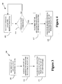
- Figure 4 conceptually illustrates a second exemplary embodiment of a method 400 for mapping architected registers to physical registers.
- a first set of architected registers has been offloaded to a memory outside of the physical registers.
- the mapping of the architected registers may have been initialized according to embodiments of the technique depicted in Figure 3 .
- Demand usage for instructions defined by the different floating-point instruction sets can be monitored (at 405). As long as there is no demand for instructions in the first instruction set associated with the first set of architected registers, or the demand usage remains (at 410) below a threshold, the system may maintain the initial and/or current mapping and continue to monitor (at 405) demand usage for the different instruction sets.
- the register mapping can be modified when the demand usage for instructions in the first instruction set rises (at 410) above a threshold.
- the threshold may be set to zero so that using any instructions from the first instruction set can trigger a re-mapping.
- the threshold maybe set to a non-zero number indicating a level of demand usage that triggers the re-mapping.
- the first set of architected registers can be mapped or re-mapped (at 415) to the physical registers when the demand usage is greater than the threshold (at 410).
- demand usage associated with the first instruction set may trigger a fault, such as the microcode fault, that allows the architected registers to be mapped (at 415) from an external cache back to the physical registers.
- the contents of the architected registers that are stored in the external cache can also be written into the appropriate locations in the physical registers.
- the physical registers that have been mapped or re-mapped (at 415) to the first set of architected registers may then be removed (at 420) from the set of rename registers supported by the physical registers.
- a fault or rest may not be triggered.
- the re-mapping (at 415) may be handled internally by the floating point architecture with less disruption. For example, a floating point unit could force a few stalls and directly copy information between the physical registers and the local side register structure.
- Figure 5 conceptually illustrates a third exemplary embodiment of a method 500 for mapping architected registers to physical registers.
- the third exemplary embodiment of the method 500 may be used independently of, in conjunction with, concurrently with, and/or in addition to the second exemplary embodiment of the method 400 depicted in Figure 4 .
- architected registers for two different floating point instruction sets have been mapped to the physical registers.
- the architected registers may have been initialized according to embodiments of the technique depicted in Figure 3 and then re-mapped to the physical registers in response to changes in demand usage as depicted in Figure 4 .
- mapping of the architected registers to the physical registers does not have to correspond to the state discussed in Figure 4 nor does the system have to have followed the route described in Figures 3-4 to arrive at a state that can utilize embodiments of the method 500.
- the method 500 may be used regardless of the particular mapping of the architected registers to the physical registers.
- Demand usage for instructions defined by the different floating-point instruction sets can be monitored (at 505). As long as the demand usage for instructions in the first instruction set associated with the first set of architected registers remains (at 510) above a threshold, the system may maintain the current mapping and continue to monitor (at 405) demand usage for the different instruction sets.
- the threshold maybe set to zero so that a re-mapping is triggered when the demand usage falls to zero.
- the threshold maybe set to a non-zero number indicating a level of demand usage that triggers the re-mapping.
- the re-mapping can be triggered when the demand usage has dropped below the threshold for a selected period of time or number of cycles.
- the first set of architected registers can be mapped (at 515) to a memory outside the physical registers, such as a cache. Information stored in the re-mapped physical registers may also be copied or written from the physical registers to the cache entries indicated by the mapping (at 515). The physical registers associated with the cached first set can then be added (at 520) to set available rename registers. Re-mapping (at 515) architected registers for the instruction set that is not being used (or is being used at a relatively low demand usage) may therefore increase the available number of rename registers, resulting in a net performance improvement for the system. For example, the out-of-order window for a processor that can perform out-of-order execution can be increased when the number of available rename registers increases.
- Embodiments of processor systems that support for floating-point register caching as described herein can be fabricated in semiconductor fabrication facilities according to various processor designs.
- a processor design can be represented as code stored on a computer readable media.
- Exemplary codes that may be used to define and/or represent the processor design may include HDL, Verilog, and the like.
- the code may be written by engineers, synthesized by other processing devices, and used to generate an intermediate representation of the processor design, e.g., netlists, GDSII data and the like.
- the intermediate representation can be stored on computer readable media and used to configure and control a manufacturing/fabrication process that is performed in a semiconductor fabrication facility.
- the semiconductor fabrication facility may include processing tools for performing deposition, photolithography, etching, polishing/planarizing, metrology, and other processes that are used to form transistors and other circuitry on semiconductor substrates.
- the processing tools can be configured and are operated using the intermediate representation, e.g. , through the use of mask works generated from GDSII data.
- the software implemented aspects of the disclosed subject matter are typically encoded on some form of program storage medium or implemented over some type of transmission medium.
- the program storage medium may be magnetic (e.g., a floppy disk or a hard drive) or optical (e.g., a compact disk read only memory, or "CD ROM"), and may be read only or random access.
- the transmission medium may be twisted wire pairs, coaxial cable, optical fiber, or some other suitable transmission medium known to the art. The disclosed subject matter is not limited by these aspects of any given implementation.
Description
- This invention relates generally to processor-based systems, and, more particularly, to register caching in processor-based systems.
- Conventional processor-based systems typically include one or more processing elements such as a central processing unit (CPU), a graphical processing unit (GPU), an accelerated processing unit (APU), and the like. The processing units include one or more processor cores that are configured to access instructions and/or data that are stored in a main memory and then execute the instructions and/or manipulate the data. Each processor core includes a floating point unit that is used to perform mathematical operations on floating point numbers when required by the executed instructions. For example, conventional floating-point units are typically designed to carry out operations such as addition, subtraction, multiplication, division, and square root. Some systems can also perform various transcendental functions such as exponential or trigonometric calculations. Floating-point operations may be handled separately from integer operations on integer numbers. The floating-point unit may also have a set of dedicated floating-point registers for storing floating-point numbers.
- Floating-point units can support multiple floating-point instruction sets. For example, the x86 architecture instruction set includes a floating-point related subset of instructions that is referred to as x87. The x87 instruction set includes instructions for basic floating point operations such as addition, subtraction and comparison, as well as for more complex numerical operation; such as the tangent and arc-tangent functions. Floating-point instructions in the x87 instruction set can use a set of architected registers (conventionally known as MMX registers) that can be mapped to physical registers in the floating-point unit. For another example, computers that include multiple processing cores may suppoli a single instruction, multiple data (SIMD) instruction set. The x86 architecture SIMD instruction set supports another floating-point related subset of instructions that arc referred to as Streaming SIMD Extensions (SSE). Floating-point instructions in the SSE instruction set can use another set of architected registers (conventionally known as XMM registers) that can also be mapped to physical registers in the floating-point unit.
-
US 2007/162726 discloses methods and apparatus for sharing storage and execution resources between architectural units in a microprocessor using a polymorphic function unit. - Different applications running on the processing unit can use the x87 floating-point instruction set, the SSE floating-point instruction set, or a mixture of the two instruction sets. Consequently, architected registers for both instruction sets are mapped to physical registers in the floating-point unit so that both sets of architected registers are available to the applications running on the processing unit. Mapping architected registers for both instruction sets to physical registers in the floating-point unit consumes area on the chip, timing resources, and power. Depending on the instruction sets used by different applications, the resources that are allocated to the different types of instruction sets may not be used, thereby reducing the efficiency of the processing unit.
- The disclosed subject matter is directed to addressing the effects of one or more of the problems set forth above. The following presents a simplified summary of the disclosed subject matter in order to provide a basic understanding of some aspects of the disclosed subject matter. This summary is not an exhaustive overview of the disclosed subject matter.
It is not intended to identify key or critical elements of the disclosed subject matter or to delineate the scope of the disclosed subject matter. Its sole purpose is to present some concepts in a simplified form as a prelude to the more detailed description that is discussed later. - In one embodiment, a method is provided for floating-point register caching. One embodiment of the method includes mapping a first set of architected registers defined by a first instruction set to a memory outside of a plurality of physical registers. The plurality of physical registers are configured to map to the first set, a second set of architected registers defined by a second construction set, and a set of rename registers. This embodiment of the method also includes adding the physical registers corresponding to the first set of architected registers to the set of rename registers.
- In another embodiment, an apparatus is provided for floating-point register caching. One embodiment of the apparatus includes a plurality of physical registers configured to be mapped to a first set of architected registers defined by a first instruction set, a second set of architected registers defined by a second instruction set, and a set of rename registers. The first set of architected registers can be mapped to a memory outside the physical registers so that the corresponding physical registers can be added to the set of rename registers.
- Another embodiment includes a computer readable media including instructions that when executed can configure a manufacturing process used to manufacture a semiconductor device that can be used for floating-point register caching. The manufactured semiconductor device includes a plurality of physical registers configured to be mapped to a first set of architected registers defined by a first instruction set, a second set of architected registers defined by a second instruction set, and a set of rename registers. The first set of architected registers can be mapped to a memory outside the physical registers so that the corresponding physical registers can be added to the set of rename registers.
- In yet another embodiment, an apparatus is provided for floating-point register caching. One embodiment of the apparatus includes a floating point unit configured to perform mathematical operations on floating point numbers and a plurality of physical registers implemented in the floating point unit and configured to store floating-point numbers. This embodiment of the apparatus also includes a memory outside of the physical registers. The memory is configured to store floating-point numbers. A first set of architected registers defined by a first instruction set, a second set of architected registers defined by a second instruction set, and a set of rename registers can be mapped to the plurality of physical registers. The first set of architected registers can also be mapped to the memory outside the physical registers so that the corresponding physical registers can be added to the set of rename registers.
- The disclosed subject matter may be understood by reference to the following description taken in conjunction with the accompanying drawings, in which like reference numerals identify like elements, and in which:
-
Figure 1 conceptually illustrates a first exemplary embodiment of a semiconductor device; -
Figure 2A conceptually illustrates a first exemplary embodiment of a mapping of architected registers to physical registers; -
Figure 2B conceptually illustrates a second exemplary embodiment of a mapping of architected registers to physical registers and a cache; -
Figure 3 conceptually illustrates a first exemplary embodiment of a method for mapping architected registers to physical registers; -
Figure 4 conceptually illustrates a second exemplary embodiment of a method for mapping architected registers to physical registers; and -
Figure 5 conceptually illustrates a third exemplary embodiment of a method for mapping architected registers to physical registers. - While the disclosed subject matter is susceptible to various modifications and alternative forms, specific embodiments thereof have been shown by way of example in the drawings and are herein described in detail. It should be understood, however, that the description herein of specific embodiments is not intended to limit the disclosed subject matter to the particular forms disclosed, but on the contrary, the intention is to cover all modifications, equivalents, and alternatives falling within the scope of the appended claims.
- Illustrative embodiments are described below. In the interest of clarity, not all features of an actual implementation are described in this specification. It will of course be appreciated that in the development of any such actual embodiment, numerous implementation-specific decisions should be made to achieve the developers' specific goals, such as compliance with system-related and business-related constraints, which will vary from one implementation to another. Moreover, it will be appreciated that such a development effort might be complex and time-consuming, but would nevertheless be a routine undertaking for those of ordinary skill in the art having the benefit of this disclosure.
- The disclosed subject matter will now be described with reference to the attached figures. Various structures, systems and devices are schematically depicted in the drawings for purposes of explanation only and so as to not obscure the present invention with details that are well known to those skilled in the art. Nevertheless, the attached drawings are included to describe and explain illustrative examples of the disclosed subject matter. The words and phrases used herein should be understood and interpreted to have a meaning consistent with the understanding of those words and phrases by those skilled in the relevant art. No special definition of a term or phrase, i.e., a definition that is different from the ordinary and customary meaning as understood by those skilled in the art, is intended to be implied by consistent usage of the term or phrase herein. To the extent that a term or phrase is intended to have a special meaning, i.e., a meaning other than that understood by skilled artisans, such a special definition will be expressly set forth in the specification in a definitional manner that directly and unequivocally provides the special definition for the term or phrase.
- Generally, the present application describes embodiments of a processor-based system that can execute instructions from multiple floating-point instruction sets. For example, the system may be able to execute instructions from the x87 floating-point instruction set and instructions from the SSE floating-point instruction set. Each instruction set is allocated a number of architected registers that can be used by the instructions when performing various floating-point operations. The architected registers may be mapped to a set of physical registers implemented in or used by the processor-based system. The physical registers may also include rename registers that can be used to rename one or more of the architected registers so that multiple instructions can be executed in parallel (e.g., concurrently) even though the instructions may refer to the same architected register. However, most of the time applications and/or code that are executing in the processor-based system use either one instruction set or the other instruction set. Only rarely does a single application use a mixture of the two floating-point instruction sets. The architected registers associated with either of the instruction sets (preferably the instruction set that is expected to be used the least) can be offloaded to an outside memory such as a cache or other register structure. The physical registers that are associated with the offloaded architected registers can then be added to the set of rename registers.
-
Figure 1 conceptually illustrates a first exemplary embodiment of asemiconductor device 100 that may be formed in or on a semiconductor wafer (or die). Thesemiconductor device 100 may formed in or on the semiconductor wafer using well known processes such as deposition, growth, photolithography, etching, planarising, polishing, annealing, and the like. In the illustrated embodiment, thedevice 100 includes a central processing unit (CPU) 105 that is configured to access instructions and/or data that are stored in themain memory 110. In the illustrated embodiment, theCPU 105 includes at least oneCPU core 115 that is used to execute the instructions and/or manipulate the data. Many processor-based systems includemultiple CPU cores 115. TheCPU 105 also implements a hierarchical (or multilevel) cache system that is used to speed access to the instructions and/or data by storing selected instructions and/or data in the caches. However, persons of ordinary skill in the art having benefit of the present disclosure should appreciate that alternative embodiments of thedevice 100 may implement different configurations of theCPU 105, such as configurations that use external caches. Moreover, the techniques described in the present application may be applied to other processors such as graphical processing units (GPUs), accelerated processing units (APUs), and the like. - The illustrated cache system includes a level 2 (L2)
cache 120 for storing copies of instructions and/or data that are stored in themain memory 110. In the illustrated embodiment, theL2 cache 120 is 16-way associative to themain memory 110 so that each line in themain memory 110 can potentially be copied to and from 16 particular lines (which are conventionally referred to as "ways") in theL2 cache 120. However, persons of ordinary skill in the art having benefit of the present disclosure should appreciate that alternative embodiments of themain memory 110 and/or theL2 cache 120 can be implemented using any associativity. Relative to themain memory 110, theL2 cache 120 may be implemented using smaller and faster memory elements. TheL2 cache 120 may also be deployed logically and/or physically closer to the CPU core 115 (relative to the main memory 110) so that information may be exchanged between theCPU core 115 and theL2 cache 120 more rapidly and/or with less latency. - The illustrated cache system also includes an
L1 cache 125 for storing copies of instructions and/or data that are stored in themain memory 110 and/or theL2 cache 120. Relative to theL2 cache 120, theL1 cache 125 may be implemented using smaller and faster memory elements so that information stored in the lines of theL1 cache 125 can be retrieved quickly by theCPU 105. TheL1 cache 125 may also be deployed logically and/or physically closer to the CPU core 115 (relative to themain memory 110 and the L2 cache 120) so that information may be exchanged between theCPU core 115 and theL1 cache 125 more rapidly and/or with less latency (relative to communication with themain memory 110 and the L2 cache 120). Persons of ordinary skill in the art having benefit of the present disclosure should appreciate that theL1 cache 125 and theL2 cache 120 represent one exemplary embodiment of a multi-level hierarchical cache memory system. Alternative embodiments may use different multilevel caches including elements such as L0 caches, L1 caches, L2 caches, L3 caches, and the like. - In the illustrated embodiment, the
L1 cache 125 is separated into level 1 (L1) caches for storing instructions and data, which are referred to as the L1-I cache 130 and the L1-D cache 135. Separating or partitioning theL1 cache 125 into an L1-I cache 130 for storing only instructions and an L1-D cache 135 for storing only data may allow these caches to be deployed closer to the entities that are likely to request instructions and/or data, respectively. Consequently, this arrangement may reduce contention, wire delays, and generally decrease latency associated with instructions and data. In one embodiment, a replacement policy dictates that the lines in the L1-I cache 130 are replaced with instructions from theL2 cache 120 and the lines in the L1-D cache 135 are replaced with data from theL2 cache 120. However, persons of ordinary skill in the art should appreciate that alternative embodiments of theL1 cache 125 may not be partitioned into separate instruction-only and data-onlycaches caches main memory 110 and invalidating other lines in thecaches CPU 105, such as a RESET or a write-back-invalidate (WBINVD) instruction. - Processor-based systems utilize two basic memory access instructions: a store that puts (or stores) information in a memory location such as a register and a load that reads information out of a memory location. The
CPU core 115 can execute programs that are formed using instructions such as loads and stores. In the illustrated embodiment, programs are stored in themain memory 110 and the instructions are kept in program order, which indicates the logical order for execution of the instructions so that the program operates correctly. For example, themain memory 110 may store instructions for aprogram 140 that includes the stores S1, S2 and the load L1 in program order. Persons of ordinary skill in the art having benefit of the present disclosure should appreciate that theprogram 140 may also include other instructions that may be performed earlier or later in the program order of theprogram 140. - The illustrated embodiment of the
CPU core 115 includes adecoder 145 that selects and decodes program instructions so that they can be executed by theCPU core 115. In the illustrated embodiment, theCPU core 115 is an out-of-order processor that can execute instructions in an order that differs from the program order of the instructions in the associated program. For example, thedecoder 145 may select and/or decode instructions from theprogram 140 in the order L1, S1, S2, which differs from the program order of theprogram 140 because the load L1 is picked before the stores S1, S2. Thedecoder 145 can dispatch, send, or provide the decoded instructions to a load/store unit 150. In the illustrated embodiment, the load/store unit 150 implements one or more store and/orload queues store unit 150 may also implement an emulated memory (E-MEM) 165 that can emulate or imitate operations of other memory elements in thesystem 100. - The
store queues 155 shown in the illustrated embodiment are used to hold the stores and associated data. The data location for each store is indicated by a linear address, which may be translated into a physical address by theCPU core 115 so that data can be accessed from themain memory 110 and/or one of thecaches CPU core 115 may therefore be electronically and/or communicatively coupled to a translation look aside buffer (TLB) 170 that holds information that is used to translate linear addresses into physical addresses. When a store (such as S1 or S2) is picked, the store checks theTLB 170 and/or thedata caches store queue 155 to wait for data. Theload queues 160 shown in the illustrated embodiment are used to hold the loads and associated data. Load data may also be indicated by linear addresses and so theCPU core 115 may translate the linear addresses for load data into a physical address using information stored in theTLB 170. In the illustrated embodiment, when a load (such as L1) is picked, the load checks theTLB 170 and/or thedata caches store queue 155 for address matches. Alternatively, linear addresses can be used to check thestore queue 155 for address matches. If an address (linear or physical depending on the embodiment) in thestore queue 155 matches the address of the data used by the load, then store-to-load forwarding can be used to forward the data from thestore queue 155 to the load in theload queue 160. - The
CPU core 115 may also implement other functional elements. In the illustrated embodiment, theCPU core 115 includes a floatingpoint unit 175 that is used to perform mathematical operations on floating point numbers when required by the executed instructions. For example, the floating-point unit 175 may be designed to carry out operations such as addition, subtraction, multiplication, division, and square root. Alternative embodiments of the floating-point unit 175 may also perform various transcendental functions such as exponential or trigonometric calculations. The floating-point unit 175 implements aregister structure 180 that includes a plurality of physical registers 185 (only one indicated by a distinguishing numeral) that are used to hold floating-point numbers. Thephysical registers 185 can be mapped to architected registers associated with or defined by different floating-point instruction sets. In the illustrated embodiment, one portion of thephysical registers 185 can be mapped to architected registers (MMX) defined by the x87 floating-point instruction set and another portion of thephysical registers 185 can be mapped to architected registers (XMM) defined by the SSE floating-point instruction set. The remaining portion of thephysical registers 185 can be used as rename registers (REN), e.g., for supporting parallel and/or concurrent execution of instructions in an out-of-order processing environment. - In one embodiment, a first set of architected registers defined by a first instruction set (e.g., the architected registers (MMX) defined by the x87 floating-point instruction set) may be mapped to a memory location that is outside the
physical registers 185, such as one or more of thecaches memory 165. Thephysical registers 185 corresponding to the first set of architected registers can then be added to the set of rename registers. Mapping some of the architected registers to memory locations outside of thephysical registers 185 therefore frees up additional registers for use as rename registers. The additional rename registers allow the system to use additional renames, which can increase the parallelism of the environment by allowing additional instructions to be executed concurrently. Increasing the number of renames may therefore increase the out-of-order window and improve the performance of thesystem 100. -
Figure 2A conceptually illustrates a first exemplary embodiment of a mapping of architected registers 200(1-3) tophysical registers 205. In the illustrated embodiment, the architectedregisters 200 include architected registers 200(1) defined for the x87 floating-point instruction set, architected registers 200(2) that are allocated as temporary registers for microcode, and architected registers 200(3) defined for the SSE floating-point instruction set. For example, the architectedregisters 200 may be defined are configured to provide eight architected registers 200(1), eight architected registers 200(2), and 32 architected registers 200(3). In the illustrated embodiment, thephysical registers 205 include entries that can be mapped to the architectedregisters 200 and/or used as a rename registers, as indicated by the block arrows. For example, thephysical registers 205 may include 88 entries so that 48 entries can be mapped to the architectedregisters 200 and the other 40 entries can be used as rename registers. However, the number of the architectedregisters 200 and/or the number ofphysical registers 205 is a matter of design choice and may be different in alternative embodiments. -
Figure 2B conceptually illustrates a second exemplary embodiment of a mapping of architected registers to physical registers and a cache. In the illustrated embodiment, a portion of the architectedregisters 200 are mapped to memory and/or register structures that are located outside of the physical registers 205. For example, a portion of the architectedregisters 200 may be mapped to acache 210. As discussed herein, the outside memory may include various caches implemented in the processor system, emulated memory, and the like. In alternative embodiments, a portion of the architectedregisters 200 that are mapped to thecache 210 may include some or all of the architectedregisters 200 associated with a particular instruction set. For example, as shown inFigure 2B , the architected registers 200(1) defined for the x87 floating-point instruction set can be mapped to thecache 210. However, persons of ordinary skill in the art having benefit of the present disclosure should appreciate that this mapping is intended to be illustrative. In alternative embodiments, architectedregisters 200 associated with different instruction sets can be mapped to thecache 210. Moreover, a portion of one or more of the architectedregisters 200 that includes less than all of the entries associated with a particular instruction set can be mapped to thecache 210. - The first and second exemplary embodiments of the register mapping shown in
Figures 2A and 2B may represent two states of the architectedregisters 200, thephysical registers 205, and thecache 210. In one embodiment, the processor system may be initialized into either one of these states, e.g., depending on the expected demand usage associated with the different registers and/or instruction sets. Furthermore, in some embodiments the processor system may transition between these two states dynamically. For example, the system may be initialized into the state illustrated inFigure 2B so that additional rename registers are available when demand usage for the x87 instruction set associated with the architected registers 200(1) is expected to be small. However, if the processor system determines that demand usage for the x87 floating-point instructions has increased, the mapping of the architectedregisters 200 can be changed so that the system shifts into the state illustrated inFigure 2A . - Persons of ordinary skill in the art having benefit of the present disclosure should appreciate that this particular set of register states and state transitions depicted in
Figures 2A and 2B is intended to be illustrative. In alternative embodiments, states representing other mappings between the architectedregisters 200, thephysical registers 205, and thecache 210 can be used and other criteria for transitioning between the states can be defined. For example, the mappings from the architectedregisters 200 to thephysical registers 205 and/or thecache 210 depicted inFigures 2A and 2B are relatively ordered and may be sequential and/or block-based. However, in alternative embodiments, other mappings can be used. For example, any of the entries in the architectedregisters 200 could be mapped to any entries in thephysical registers 205 and/or thecache 210. In some cases, the mapping may be random or based on other criteria. -
Figure 3 conceptually illustrates a first exemplary embodiment of amethod 300 for mapping architected registers to physical registers. In the illustrated embodiment, the physical registers are configured so that architected registers associated with two or more different floating-point instruction sets can be mapped to the physical registers and used when the processor system is executing instructions. The physical registers also include additional entries that can be used as rename registers. The mapping can be initialized so that some of the architected registers are mapped to a memory outside of the physical registers. In the illustrated embodiment, a first set of architected registers (which are drawn from architected registers defined for a first floating-point instruction set) is mapped (at 305) to a cache that is located physically and/or logically outside of the physical registers. A second set of architected registers is mapped (at 310) to the physical registers. The unmapped physical registers that were intended to be mapped to the first set of architected registers can then be added (at 315) to the set of rename registers that are supported by the physical registers. -
Figure 4 conceptually illustrates a second exemplary embodiment of amethod 400 for mapping architected registers to physical registers. In the illustrated embodiment, a first set of architected registers has been offloaded to a memory outside of the physical registers. For example, the mapping of the architected registers may have been initialized according to embodiments of the technique depicted inFigure 3 . Demand usage for instructions defined by the different floating-point instruction sets can be monitored (at 405). As long as there is no demand for instructions in the first instruction set associated with the first set of architected registers, or the demand usage remains (at 410) below a threshold, the system may maintain the initial and/or current mapping and continue to monitor (at 405) demand usage for the different instruction sets. - The register mapping can be modified when the demand usage for instructions in the first instruction set rises (at 410) above a threshold. In one embodiment, the threshold may be set to zero so that using any instructions from the first instruction set can trigger a re-mapping. Alternatively, the threshold maybe set to a non-zero number indicating a level of demand usage that triggers the re-mapping. The first set of architected registers can be mapped or re-mapped (at 415) to the physical registers when the demand usage is greater than the threshold (at 410). For example, demand usage associated with the first instruction set may trigger a fault, such as the microcode fault, that allows the architected registers to be mapped (at 415) from an external cache back to the physical registers. The contents of the architected registers that are stored in the external cache can also be written into the appropriate locations in the physical registers. The physical registers that have been mapped or re-mapped (at 415) to the first set of architected registers may then be removed (at 420) from the set of rename registers supported by the physical registers. In alternative embodiments that use a side register structure such as an E-MEM in the floating point unit, a fault or rest may not be triggered. Instead, the re-mapping (at 415) may be handled internally by the floating point architecture with less disruption. For example, a floating point unit could force a few stalls and directly copy information between the physical registers and the local side register structure.
-
Figure 5 conceptually illustrates a third exemplary embodiment of amethod 500 for mapping architected registers to physical registers. The third exemplary embodiment of themethod 500 may be used independently of, in conjunction with, concurrently with, and/or in addition to the second exemplary embodiment of themethod 400 depicted inFigure 4 . In the third exemplary embodiment, architected registers for two different floating point instruction sets have been mapped to the physical registers. For example, the architected registers may have been initialized according to embodiments of the technique depicted inFigure 3 and then re-mapped to the physical registers in response to changes in demand usage as depicted inFigure 4 . However, the mapping of the architected registers to the physical registers does not have to correspond to the state discussed inFigure 4 nor does the system have to have followed the route described inFigures 3-4 to arrive at a state that can utilize embodiments of themethod 500. In alternative embodiments, themethod 500 may be used regardless of the particular mapping of the architected registers to the physical registers. - Demand usage for instructions defined by the different floating-point instruction sets can be monitored (at 505). As long as the demand usage for instructions in the first instruction set associated with the first set of architected registers remains (at 510) above a threshold, the system may maintain the current mapping and continue to monitor (at 405) demand usage for the different instruction sets. In one embodiment, the threshold maybe set to zero so that a re-mapping is triggered when the demand usage falls to zero. Alternatively, the threshold maybe set to a non-zero number indicating a level of demand usage that triggers the re-mapping. In yet another alternative embodiment, the re-mapping can be triggered when the demand usage has dropped below the threshold for a selected period of time or number of cycles. For example, if a selected number of clock cycles go by (e.g., 10K cycles) and either the registers allocated to the x87 instruction set or the registers allocated to the SSE instruction set aren't being used, a fault can be forced, the registers saved out of the type that is not being used currently, and then processing may continue. However, if the floating point unit is not executing any instructions, there is no performance tradeoff and so forcing the save may not be necessary.
- When the demand usage has fallen below a threshold (perhaps for a selected time interval), the first set of architected registers can be mapped (at 515) to a memory outside the physical registers, such as a cache. Information stored in the re-mapped physical registers may also be copied or written from the physical registers to the cache entries indicated by the mapping (at 515). The physical registers associated with the cached first set can then be added (at 520) to set available rename registers. Re-mapping (at 515) architected registers for the instruction set that is not being used (or is being used at a relatively low demand usage) may therefore increase the available number of rename registers, resulting in a net performance improvement for the system. For example, the out-of-order window for a processor that can perform out-of-order execution can be increased when the number of available rename registers increases.
- Embodiments of processor systems that support for floating-point register caching as described herein (such as the processor system 100) can be fabricated in semiconductor fabrication facilities according to various processor designs. In one embodiment, a processor design can be represented as code stored on a computer readable media. Exemplary codes that may be used to define and/or represent the processor design may include HDL, Verilog, and the like. The code may be written by engineers, synthesized by other processing devices, and used to generate an intermediate representation of the processor design, e.g., netlists, GDSII data and the like. The intermediate representation can be stored on computer readable media and used to configure and control a manufacturing/fabrication process that is performed in a semiconductor fabrication facility. The semiconductor fabrication facility may include processing tools for performing deposition, photolithography, etching, polishing/planarizing, metrology, and other processes that are used to form transistors and other circuitry on semiconductor substrates. The processing tools can be configured and are operated using the intermediate representation, e.g., through the use of mask works generated from GDSII data.
- Portions of the disclosed subject matter and corresponding detailed description are presented in terms of software, or algorithms and symbolic representations of operations on data bits within a computer memory. These descriptions and representations are the ones by which those of ordinary skill in the art effectively convey the substance of their work to others of ordinary skill in the art. An algorithm, as the term is used here, and as it is used generally, is conceived to be a self-consistent sequence of steps leading to a desired result. The steps are those requiring physical manipulations of physical quantities. Usually, though not necessarily, these quantities take the form of optical, electrical, or magnetic signals capable of being stored, transferred, combined, compared, and otherwise manipulated. It has proven convenient at times, principally for reasons of common usage, to refer to these signals as bits, values, elements, symbols, characters, terms, numbers, or the like.
- It should be borne in mind, however, that all of these and similar terms are to be associated with the appropriate physical quantities and are merely convenient labels applied to these quantities. Unless specifically stated otherwise, or as is apparent from the discussion, terms such as "processing" or "computing" or "calculating" or "determining" or "displaying" or the like, refer to the action and processes of a computer system, or similar electronic computing device, that manipulates and transforms data represented as physical, electronic quantities within the computer system's registers and memories into other data similarly represented as physical quantities within the computer system memories or registers or other such information storage, transmission or display devices.
- Note also that the software implemented aspects of the disclosed subject matter are typically encoded on some form of program storage medium or implemented over some type of transmission medium. The program storage medium may be magnetic (e.g., a floppy disk or a hard drive) or optical (e.g., a compact disk read only memory, or "CD ROM"), and may be read only or random access. Similarly, the transmission medium may be twisted wire pairs, coaxial cable, optical fiber, or some other suitable transmission medium known to the art. The disclosed subject matter is not limited by these aspects of any given implementation.
- The particular embodiments disclosed above are illustrative only, as the disclosed subject matter may be modified and practiced in different but equivalent manners apparent to those skilled in the art having the benefit of the teachings herein. Furthermore, no limitations are intended to the details of construction or design herein shown, other than as described in the claims below. It is therefore evident that the particular embodiments disclosed above may be altered or modified and all such variations are considered within the scope of the disclosed subject matter. Accordingly, the protection sought herein is as set forth in the claims below.
Claims (10)
- A method within an apparatus comprising a plurality of physical registers wherein the plurality of physical registers (185) are configured to map to a first set of architected registers (MMX) defined by a first instruction set, a second set of architected registers (XMM) defined by a second instruction set, and a set of rename registers (REN) characterized by the steps of:mapping the first set of architected registers (MMX) to a memory (120, 125, 130, 135, 165) outside of the plurality of physical registers (185); andadding the physical registers corresponding to the first set of architected registers to the set of rename registers in response to said mapping.
- The method of claim 1, wherein mapping the first set of architected registers comprises initializing a mapping of the physical registers to the second set of architected registers and the set of rename registers, initializing a mapping of the first set of architected registers to a cache memory outside of the plurality of physical registers, re-mapping the first set of architected registers to the physical registers in response to demand usage associated with instructions from the first instruction set, and removing the physical registers corresponding to the re-mapped first set of architected registers from the set of rename registers.
- The method of claim 1, wherein mapping the first set of architected registers to the memory comprises mapping the first set of architected registers to a cache memory outside of the plurality of physical registers.
- The method of claim 1, wherein mapping the first set of architected registers to the memory comprises re-mapping the first set of architected registers from the physical registers to the memory in response to a decrease in demand usage associated with instructions from the first instruction set.
- The method of claim 1, comprising re-mapping the first set of architected registers from the memory to the physical registers and removing the physical registers corresponding to the re-mapped first set from the set of rename registers in response to an increase in demand usage associated with instructions from the first instruction set.
- An apparatus, comprising:a plurality of physical registers (185) configured to be mapped to a first set of architected registers (MMX) defined by a first instruction set, a second set of architected registers (XMM) defined by a second instruction set, and a set of rename registers (REN), characterized in that the first set of architected registers is configured to be mapped to a memory (120, 125, 130, 135, 165) outside the physical registers, and wherein the corresponding physical registers are added to the set of rename registers in response to said mapping.
- The apparatus of claim 6, wherein the plurality of physical registers are configured to be initialized so that the physical registers arc mapped to the second set of architected registers and the set of rename registers, and wherein the first set of architected registers are mapped to the memory outside the physical registers, and wherein the physical registers are configured so that the first set of architected registers can be re-mapped to the physical registers in response to demand usage associated with instructions from the first instruction set, and wherein the physical registers corresponding to the re-mapped first set of architected registers can be removed from the set of rename registers in response to the demand usage associated with instructions from the first instruction set.
- The apparatus of claim 6, comprising a cache memory, and wherein the physical registers are configured so that the first set of architected registers can be mapped to a cache memory.
- The apparatus of claim 6, wherein the physical registers are configured so that the first set of architected registers can be mapped from the physical registers to the memory in response to a decrease in demand usage associated with instructions from the first instruction set, and wherein the physical registers are configured so that the first set of architected registers can be re-mapped from the memory to the physical registers in response to an increase in demand usage associated with instructions from the first instruction set and the physical registers corresponding to the re-mapped first set can be removed from the set of rename registers in response to the increase in demand usage associated with instructions from the first instruction set, and wherein the physical registers are configured so that the second set of architected registers can be mapped from the physical registers to the memory in response to a decrease in demand usage associated with instructions from the second instruction set and the physical registers corresponding to the second set can be mapped to the set of rename registers in response to the decrease in demand usage associated with instructions from the second instruction set.
- A computer readable media including instructions that when executed can configure a manufacturing process used to manufacture a semiconductor device that comprises the apparatus defined in any of claim 6-9.
Applications Claiming Priority (2)
| Application Number | Priority Date | Filing Date | Title |
|---|---|---|---|
| US12/900,124 US9626190B2 (en) | 2010-10-07 | 2010-10-07 | Method and apparatus for floating point register caching |
| PCT/US2011/054688 WO2012047833A1 (en) | 2010-10-07 | 2011-10-04 | Method and apparatus for floating point register caching |
Publications (2)
| Publication Number | Publication Date |
|---|---|
| EP2625599A1 EP2625599A1 (en) | 2013-08-14 |
| EP2625599B1 true EP2625599B1 (en) | 2014-09-03 |
Family
ID=44863229
Family Applications (1)
| Application Number | Title | Priority Date | Filing Date |
|---|---|---|---|
| EP11771344.6A Active EP2625599B1 (en) | 2010-10-07 | 2011-10-04 | Method and apparatus for floating point register caching |
Country Status (6)
| Country | Link |
|---|---|
| US (1) | US9626190B2 (en) |
| EP (1) | EP2625599B1 (en) |
| JP (1) | JP5703382B2 (en) |
| KR (1) | KR101797187B1 (en) |
| CN (1) | CN103262028B (en) |
| WO (1) | WO2012047833A1 (en) |
Families Citing this family (16)
| Publication number | Priority date | Publication date | Assignee | Title |
|---|---|---|---|---|
| US8914615B2 (en) * | 2011-12-02 | 2014-12-16 | Arm Limited | Mapping same logical register specifier for different instruction sets with divergent association to architectural register file using common address format |
| US9632947B2 (en) * | 2013-08-19 | 2017-04-25 | Intel Corporation | Systems and methods for acquiring data for loads at different access times from hierarchical sources using a load queue as a temporary storage buffer and completing the load early |
| JP6511462B2 (en) * | 2013-10-27 | 2019-05-15 | アドバンスト・マイクロ・ディバイシズ・インコーポレイテッドAdvanced Micro Devices Incorporated | Processor and method for floating point register aliasing |
| JP6493088B2 (en) * | 2015-08-24 | 2019-04-03 | 富士通株式会社 | Arithmetic processing device and control method of arithmetic processing device |
| US10740108B2 (en) | 2017-04-18 | 2020-08-11 | International Business Machines Corporation | Management of store queue based on restoration operation |
| US10649785B2 (en) | 2017-04-18 | 2020-05-12 | International Business Machines Corporation | Tracking changes to memory via check and recovery |
| US10545766B2 (en) | 2017-04-18 | 2020-01-28 | International Business Machines Corporation | Register restoration using transactional memory register snapshots |
| US10782979B2 (en) | 2017-04-18 | 2020-09-22 | International Business Machines Corporation | Restoring saved architected registers and suppressing verification of registers to be restored |
| US11010192B2 (en) | 2017-04-18 | 2021-05-18 | International Business Machines Corporation | Register restoration using recovery buffers |
| US10572265B2 (en) | 2017-04-18 | 2020-02-25 | International Business Machines Corporation | Selecting register restoration or register reloading |
| US10963261B2 (en) | 2017-04-18 | 2021-03-30 | International Business Machines Corporation | Sharing snapshots across save requests |
| US10838733B2 (en) | 2017-04-18 | 2020-11-17 | International Business Machines Corporation | Register context restoration based on rename register recovery |
| US10592164B2 (en) | 2017-11-14 | 2020-03-17 | International Business Machines Corporation | Portions of configuration state registers in-memory |
| US10761983B2 (en) * | 2017-11-14 | 2020-09-01 | International Business Machines Corporation | Memory based configuration state registers |
| US10853078B2 (en) * | 2018-12-21 | 2020-12-01 | Intel Corporation | Method and apparatus for supporting speculative memory optimizations |
| US20220137925A1 (en) * | 2019-02-20 | 2022-05-05 | Optimum Semiconductor Technologies Inc. | Device and method for hardware-efficient adaptive calculation of floating-point trigonometric functions using coordinate rotate digital computer (cordic) |
Family Cites Families (13)
| Publication number | Priority date | Publication date | Assignee | Title |
|---|---|---|---|---|
| JP2000056969A (en) * | 1998-08-07 | 2000-02-25 | Matsushita Electric Ind Co Ltd | Register file |
| US6237076B1 (en) | 1998-08-19 | 2001-05-22 | International Business Machines Corporation | Method for register renaming by copying a 32 bits instruction directly or indirectly to a 64 bits instruction |
| US6425072B1 (en) | 1999-08-31 | 2002-07-23 | Advanced Micro Devices, Inc. | System for implementing a register free-list by using swap bit to select first or second register tag in retire queue |
| US6772317B2 (en) * | 2001-05-17 | 2004-08-03 | Intel Corporation | Method and apparatus for optimizing load memory accesses |
| US7065631B2 (en) * | 2002-04-09 | 2006-06-20 | Sun Microsystems, Inc. | Software controllable register map |
| US7127592B2 (en) * | 2003-01-08 | 2006-10-24 | Sun Microsystems, Inc. | Method and apparatus for dynamically allocating registers in a windowed architecture |
| US7725682B2 (en) * | 2006-01-10 | 2010-05-25 | International Business Machines Corporation | Method and apparatus for sharing storage and execution resources between architectural units in a microprocessor using a polymorphic function unit |
| US7506139B2 (en) * | 2006-07-12 | 2009-03-17 | International Business Machines Corporation | Method and apparatus for register renaming using multiple physical register files and avoiding associative search |
| US7475224B2 (en) * | 2007-01-03 | 2009-01-06 | International Business Machines Corporation | Register map unit supporting mapping of multiple register specifier classes |
| US8140780B2 (en) * | 2008-12-31 | 2012-03-20 | Micron Technology, Inc. | Systems, methods, and devices for configuring a device |
| US8266411B2 (en) | 2009-02-05 | 2012-09-11 | International Business Machines Corporation | Instruction set architecture with instruction characteristic bit indicating a result is not of architectural importance |
| US8707015B2 (en) | 2010-07-01 | 2014-04-22 | Advanced Micro Devices, Inc. | Reclaiming physical registers renamed as microcode architectural registers to be available for renaming as instruction set architectural registers based on an active status indicator |
| US8972701B2 (en) | 2011-12-06 | 2015-03-03 | Arm Limited | Setting zero bits in architectural register for storing destination operand of smaller size based on corresponding zero flag attached to renamed physical register |
-
2010
- 2010-10-07 US US12/900,124 patent/US9626190B2/en active Active
-
2011
- 2011-10-04 JP JP2013532870A patent/JP5703382B2/en active Active
- 2011-10-04 WO PCT/US2011/054688 patent/WO2012047833A1/en active Application Filing
- 2011-10-04 CN CN201180059045.0A patent/CN103262028B/en active Active
- 2011-10-04 KR KR1020137008998A patent/KR101797187B1/en active IP Right Grant
- 2011-10-04 EP EP11771344.6A patent/EP2625599B1/en active Active
Also Published As
| Publication number | Publication date |
|---|---|
| KR101797187B1 (en) | 2017-11-13 |
| US9626190B2 (en) | 2017-04-18 |
| WO2012047833A1 (en) | 2012-04-12 |
| KR20130127437A (en) | 2013-11-22 |
| JP5703382B2 (en) | 2015-04-15 |
| US20120089807A1 (en) | 2012-04-12 |
| CN103262028A (en) | 2013-08-21 |
| JP2014500993A (en) | 2014-01-16 |
| EP2625599A1 (en) | 2013-08-14 |
| CN103262028B (en) | 2016-02-10 |
Similar Documents
| Publication | Publication Date | Title |
|---|---|---|
| EP2625599B1 (en) | Method and apparatus for floating point register caching | |
| US8713263B2 (en) | Out-of-order load/store queue structure | |
| EP2476060B1 (en) | Store aware prefetching for a datastream | |
| JP6143872B2 (en) | Apparatus, method, and system | |
| US9448936B2 (en) | Concurrent store and load operations | |
| US9952989B2 (en) | Aggregation of interrupts using event queues | |
| US8412911B2 (en) | System and method to invalidate obsolete address translations | |
| US9213640B2 (en) | Promoting transactions hitting critical beat of cache line load requests | |
| US20180349280A1 (en) | Snoop filtering for multi-processor-core systems | |
| US20130024647A1 (en) | Cache backed vector registers | |
| US20140129806A1 (en) | Load/store picker | |
| US9489203B2 (en) | Pre-fetching instructions using predicted branch target addresses | |
| WO2006132798A2 (en) | Microprocessor including a configurable translation lookaside buffer | |
| US8645588B2 (en) | Pipelined serial ring bus | |
| WO2014084918A1 (en) | Providing extended cache replacement state information | |
| US20120054448A1 (en) | Method and apparatus for adapting aggressiveness of a pre-fetcher | |
| US20090300319A1 (en) | Apparatus and method for memory structure to handle two load operations | |
| CN111752616A (en) | System, apparatus and method for symbolic memory address generation | |
| US20140310500A1 (en) | Page cross misalign buffer | |
| US20030182539A1 (en) | Storing execution results of mispredicted paths in a superscalar computer processor | |
| JP2023500604A (en) | Shadow latches in the shadow latch configuration register file for storing threads | |
| WO2013147895A2 (en) | Dynamic physical register use threshold adjustment and cross thread stall in multi-threaded processors |
Legal Events
| Date | Code | Title | Description |
|---|---|---|---|
| PUAI | Public reference made under article 153(3) epc to a published international application that has entered the european phase |
Free format text: ORIGINAL CODE: 0009012 |
|
| 17P | Request for examination filed |
Effective date: 20130430 |
|
| AK | Designated contracting states |
Kind code of ref document: A1 Designated state(s): AL AT BE BG CH CY CZ DE DK EE ES FI FR GB GR HR HU IE IS IT LI LT LU LV MC MK MT NL NO PL PT RO RS SE SI SK SM TR |
|
| DAX | Request for extension of the european patent (deleted) | ||
| GRAP | Despatch of communication of intention to grant a patent |
Free format text: ORIGINAL CODE: EPIDOSNIGR1 |
|
| INTG | Intention to grant announced |
Effective date: 20140415 |
|
| GRAS | Grant fee paid |
Free format text: ORIGINAL CODE: EPIDOSNIGR3 |
|
| GRAA | (expected) grant |
Free format text: ORIGINAL CODE: 0009210 |
|
| AK | Designated contracting states |
Kind code of ref document: B1 Designated state(s): AL AT BE BG CH CY CZ DE DK EE ES FI FR GB GR HR HU IE IS IT LI LT LU LV MC MK MT NL NO PL PT RO RS SE SI SK SM TR |
|
| REG | Reference to a national code |
Ref country code: GB Ref legal event code: FG4D |
|
| REG | Reference to a national code |
Ref country code: CH Ref legal event code: EP Ref country code: AT Ref legal event code: REF Ref document number: 685913 Country of ref document: AT Kind code of ref document: T Effective date: 20140915 |
|
| REG | Reference to a national code |
Ref country code: IE Ref legal event code: FG4D |
|
| REG | Reference to a national code |
Ref country code: DE Ref legal event code: R096 Ref document number: 602011009678 Country of ref document: DE Effective date: 20141016 |
|
| REG | Reference to a national code |
Ref country code: AT Ref legal event code: MK05 Ref document number: 685913 Country of ref document: AT Kind code of ref document: T Effective date: 20140903 |
|
| PG25 | Lapsed in a contracting state [announced via postgrant information from national office to epo] |
Ref country code: FI Free format text: LAPSE BECAUSE OF FAILURE TO SUBMIT A TRANSLATION OF THE DESCRIPTION OR TO PAY THE FEE WITHIN THE PRESCRIBED TIME-LIMIT Effective date: 20140903 Ref country code: GR Free format text: LAPSE BECAUSE OF FAILURE TO SUBMIT A TRANSLATION OF THE DESCRIPTION OR TO PAY THE FEE WITHIN THE PRESCRIBED TIME-LIMIT Effective date: 20141204 Ref country code: ES Free format text: LAPSE BECAUSE OF FAILURE TO SUBMIT A TRANSLATION OF THE DESCRIPTION OR TO PAY THE FEE WITHIN THE PRESCRIBED TIME-LIMIT Effective date: 20140903 Ref country code: NO Free format text: LAPSE BECAUSE OF FAILURE TO SUBMIT A TRANSLATION OF THE DESCRIPTION OR TO PAY THE FEE WITHIN THE PRESCRIBED TIME-LIMIT Effective date: 20141203 Ref country code: LT Free format text: LAPSE BECAUSE OF FAILURE TO SUBMIT A TRANSLATION OF THE DESCRIPTION OR TO PAY THE FEE WITHIN THE PRESCRIBED TIME-LIMIT Effective date: 20140903 Ref country code: SE Free format text: LAPSE BECAUSE OF FAILURE TO SUBMIT A TRANSLATION OF THE DESCRIPTION OR TO PAY THE FEE WITHIN THE PRESCRIBED TIME-LIMIT Effective date: 20140903 |
|
| REG | Reference to a national code |
Ref country code: NL Ref legal event code: VDEP Effective date: 20140903 |
|
| REG | Reference to a national code |
Ref country code: LT Ref legal event code: MG4D |
|
| PG25 | Lapsed in a contracting state [announced via postgrant information from national office to epo] |
Ref country code: AT Free format text: LAPSE BECAUSE OF FAILURE TO SUBMIT A TRANSLATION OF THE DESCRIPTION OR TO PAY THE FEE WITHIN THE PRESCRIBED TIME-LIMIT Effective date: 20140903 Ref country code: RS Free format text: LAPSE BECAUSE OF FAILURE TO SUBMIT A TRANSLATION OF THE DESCRIPTION OR TO PAY THE FEE WITHIN THE PRESCRIBED TIME-LIMIT Effective date: 20140903 Ref country code: CY Free format text: LAPSE BECAUSE OF FAILURE TO SUBMIT A TRANSLATION OF THE DESCRIPTION OR TO PAY THE FEE WITHIN THE PRESCRIBED TIME-LIMIT Effective date: 20140903 Ref country code: LV Free format text: LAPSE BECAUSE OF FAILURE TO SUBMIT A TRANSLATION OF THE DESCRIPTION OR TO PAY THE FEE WITHIN THE PRESCRIBED TIME-LIMIT Effective date: 20140903 Ref country code: HR Free format text: LAPSE BECAUSE OF FAILURE TO SUBMIT A TRANSLATION OF THE DESCRIPTION OR TO PAY THE FEE WITHIN THE PRESCRIBED TIME-LIMIT Effective date: 20140903 |
|
| PG25 | Lapsed in a contracting state [announced via postgrant information from national office to epo] |
Ref country code: NL Free format text: LAPSE BECAUSE OF FAILURE TO SUBMIT A TRANSLATION OF THE DESCRIPTION OR TO PAY THE FEE WITHIN THE PRESCRIBED TIME-LIMIT Effective date: 20140903 |
|
| PG25 | Lapsed in a contracting state [announced via postgrant information from national office to epo] |
Ref country code: PT Free format text: LAPSE BECAUSE OF FAILURE TO SUBMIT A TRANSLATION OF THE DESCRIPTION OR TO PAY THE FEE WITHIN THE PRESCRIBED TIME-LIMIT Effective date: 20150105 Ref country code: RO Free format text: LAPSE BECAUSE OF FAILURE TO SUBMIT A TRANSLATION OF THE DESCRIPTION OR TO PAY THE FEE WITHIN THE PRESCRIBED TIME-LIMIT Effective date: 20140903 Ref country code: SK Free format text: LAPSE BECAUSE OF FAILURE TO SUBMIT A TRANSLATION OF THE DESCRIPTION OR TO PAY THE FEE WITHIN THE PRESCRIBED TIME-LIMIT Effective date: 20140903 Ref country code: EE Free format text: LAPSE BECAUSE OF FAILURE TO SUBMIT A TRANSLATION OF THE DESCRIPTION OR TO PAY THE FEE WITHIN THE PRESCRIBED TIME-LIMIT Effective date: 20140903 Ref country code: IS Free format text: LAPSE BECAUSE OF FAILURE TO SUBMIT A TRANSLATION OF THE DESCRIPTION OR TO PAY THE FEE WITHIN THE PRESCRIBED TIME-LIMIT Effective date: 20150103 Ref country code: CZ Free format text: LAPSE BECAUSE OF FAILURE TO SUBMIT A TRANSLATION OF THE DESCRIPTION OR TO PAY THE FEE WITHIN THE PRESCRIBED TIME-LIMIT Effective date: 20140903 |
|
| PG25 | Lapsed in a contracting state [announced via postgrant information from national office to epo] |
Ref country code: PL Free format text: LAPSE BECAUSE OF FAILURE TO SUBMIT A TRANSLATION OF THE DESCRIPTION OR TO PAY THE FEE WITHIN THE PRESCRIBED TIME-LIMIT Effective date: 20140903 |
|
| REG | Reference to a national code |
Ref country code: CH Ref legal event code: PL |
|
| REG | Reference to a national code |
Ref country code: DE Ref legal event code: R097 Ref document number: 602011009678 Country of ref document: DE |
|
| PG25 | Lapsed in a contracting state [announced via postgrant information from national office to epo] |
Ref country code: BE Free format text: LAPSE BECAUSE OF NON-PAYMENT OF DUE FEES Effective date: 20141031 Ref country code: MC Free format text: LAPSE BECAUSE OF FAILURE TO SUBMIT A TRANSLATION OF THE DESCRIPTION OR TO PAY THE FEE WITHIN THE PRESCRIBED TIME-LIMIT Effective date: 20140903 |
|
| PLBE | No opposition filed within time limit |
Free format text: ORIGINAL CODE: 0009261 |
|
| STAA | Information on the status of an ep patent application or granted ep patent |
Free format text: STATUS: NO OPPOSITION FILED WITHIN TIME LIMIT |
|
| REG | Reference to a national code |
Ref country code: IE Ref legal event code: MM4A |
|
| PG25 | Lapsed in a contracting state [announced via postgrant information from national office to epo] |
Ref country code: CH Free format text: LAPSE BECAUSE OF NON-PAYMENT OF DUE FEES Effective date: 20141031 Ref country code: DK Free format text: LAPSE BECAUSE OF FAILURE TO SUBMIT A TRANSLATION OF THE DESCRIPTION OR TO PAY THE FEE WITHIN THE PRESCRIBED TIME-LIMIT Effective date: 20140903 Ref country code: LI Free format text: LAPSE BECAUSE OF NON-PAYMENT OF DUE FEES Effective date: 20141031 |
|
| REG | Reference to a national code |
Ref country code: FR Ref legal event code: ST Effective date: 20150630 |
|
| 26N | No opposition filed |
Effective date: 20150604 |
|
| PG25 | Lapsed in a contracting state [announced via postgrant information from national office to epo] |
Ref country code: FR Free format text: LAPSE BECAUSE OF NON-PAYMENT OF DUE FEES Effective date: 20141103 Ref country code: IT Free format text: LAPSE BECAUSE OF FAILURE TO SUBMIT A TRANSLATION OF THE DESCRIPTION OR TO PAY THE FEE WITHIN THE PRESCRIBED TIME-LIMIT Effective date: 20140903 |
|
| PG25 | Lapsed in a contracting state [announced via postgrant information from national office to epo] |
Ref country code: IE Free format text: LAPSE BECAUSE OF NON-PAYMENT OF DUE FEES Effective date: 20141004 |
|
| PG25 | Lapsed in a contracting state [announced via postgrant information from national office to epo] |
Ref country code: SI Free format text: LAPSE BECAUSE OF FAILURE TO SUBMIT A TRANSLATION OF THE DESCRIPTION OR TO PAY THE FEE WITHIN THE PRESCRIBED TIME-LIMIT Effective date: 20140903 |
|
| PG25 | Lapsed in a contracting state [announced via postgrant information from national office to epo] |
Ref country code: SM Free format text: LAPSE BECAUSE OF FAILURE TO SUBMIT A TRANSLATION OF THE DESCRIPTION OR TO PAY THE FEE WITHIN THE PRESCRIBED TIME-LIMIT Effective date: 20140903 |
|
| PG25 | Lapsed in a contracting state [announced via postgrant information from national office to epo] |
Ref country code: BG Free format text: LAPSE BECAUSE OF FAILURE TO SUBMIT A TRANSLATION OF THE DESCRIPTION OR TO PAY THE FEE WITHIN THE PRESCRIBED TIME-LIMIT Effective date: 20140903 |
|
| PG25 | Lapsed in a contracting state [announced via postgrant information from national office to epo] |
Ref country code: BE Free format text: LAPSE BECAUSE OF FAILURE TO SUBMIT A TRANSLATION OF THE DESCRIPTION OR TO PAY THE FEE WITHIN THE PRESCRIBED TIME-LIMIT Effective date: 20140903 Ref country code: MT Free format text: LAPSE BECAUSE OF FAILURE TO SUBMIT A TRANSLATION OF THE DESCRIPTION OR TO PAY THE FEE WITHIN THE PRESCRIBED TIME-LIMIT Effective date: 20140903 Ref country code: TR Free format text: LAPSE BECAUSE OF FAILURE TO SUBMIT A TRANSLATION OF THE DESCRIPTION OR TO PAY THE FEE WITHIN THE PRESCRIBED TIME-LIMIT Effective date: 20140903 Ref country code: LU Free format text: LAPSE BECAUSE OF NON-PAYMENT OF DUE FEES Effective date: 20141004 Ref country code: HU Free format text: LAPSE BECAUSE OF FAILURE TO SUBMIT A TRANSLATION OF THE DESCRIPTION OR TO PAY THE FEE WITHIN THE PRESCRIBED TIME-LIMIT; INVALID AB INITIO Effective date: 20111004 |
|
| PG25 | Lapsed in a contracting state [announced via postgrant information from national office to epo] |
Ref country code: MK Free format text: LAPSE BECAUSE OF FAILURE TO SUBMIT A TRANSLATION OF THE DESCRIPTION OR TO PAY THE FEE WITHIN THE PRESCRIBED TIME-LIMIT Effective date: 20140903 |
|
| PG25 | Lapsed in a contracting state [announced via postgrant information from national office to epo] |
Ref country code: AL Free format text: LAPSE BECAUSE OF FAILURE TO SUBMIT A TRANSLATION OF THE DESCRIPTION OR TO PAY THE FEE WITHIN THE PRESCRIBED TIME-LIMIT Effective date: 20140903 |
|
| P01 | Opt-out of the competence of the unified patent court (upc) registered |
Effective date: 20230530 |
|
| PGFP | Annual fee paid to national office [announced via postgrant information from national office to epo] |
Ref country code: GB Payment date: 20231018 Year of fee payment: 13 |
|
| PGFP | Annual fee paid to national office [announced via postgrant information from national office to epo] |
Ref country code: DE Payment date: 20231017 Year of fee payment: 13 |