EP2624662B1 - Led driver circuit, method of driving and vehicle light - Google Patents
Led driver circuit, method of driving and vehicle light Download PDFInfo
- Publication number
- EP2624662B1 EP2624662B1 EP13153314.3A EP13153314A EP2624662B1 EP 2624662 B1 EP2624662 B1 EP 2624662B1 EP 13153314 A EP13153314 A EP 13153314A EP 2624662 B1 EP2624662 B1 EP 2624662B1
- Authority
- EP
- European Patent Office
- Prior art keywords
- lighting
- branch
- driver
- voltage
- branches
- Prior art date
- Legal status (The legal status is an assumption and is not a legal conclusion. Google has not performed a legal analysis and makes no representation as to the accuracy of the status listed.)
- Active
Links
Images



Classifications
-
- H—ELECTRICITY
- H05—ELECTRIC TECHNIQUES NOT OTHERWISE PROVIDED FOR
- H05B—ELECTRIC HEATING; ELECTRIC LIGHT SOURCES NOT OTHERWISE PROVIDED FOR; CIRCUIT ARRANGEMENTS FOR ELECTRIC LIGHT SOURCES, IN GENERAL
- H05B45/00—Circuit arrangements for operating light-emitting diodes [LED]
- H05B45/10—Controlling the intensity of the light
-
- H—ELECTRICITY
- H05—ELECTRIC TECHNIQUES NOT OTHERWISE PROVIDED FOR
- H05B—ELECTRIC HEATING; ELECTRIC LIGHT SOURCES NOT OTHERWISE PROVIDED FOR; CIRCUIT ARRANGEMENTS FOR ELECTRIC LIGHT SOURCES, IN GENERAL
- H05B45/00—Circuit arrangements for operating light-emitting diodes [LED]
- H05B45/40—Details of LED load circuits
- H05B45/44—Details of LED load circuits with an active control inside an LED matrix
-
- H—ELECTRICITY
- H05—ELECTRIC TECHNIQUES NOT OTHERWISE PROVIDED FOR
- H05B—ELECTRIC HEATING; ELECTRIC LIGHT SOURCES NOT OTHERWISE PROVIDED FOR; CIRCUIT ARRANGEMENTS FOR ELECTRIC LIGHT SOURCES, IN GENERAL
- H05B45/00—Circuit arrangements for operating light-emitting diodes [LED]
- H05B45/40—Details of LED load circuits
- H05B45/44—Details of LED load circuits with an active control inside an LED matrix
- H05B45/46—Details of LED load circuits with an active control inside an LED matrix having LEDs disposed in parallel lines
-
- H—ELECTRICITY
- H05—ELECTRIC TECHNIQUES NOT OTHERWISE PROVIDED FOR
- H05B—ELECTRIC HEATING; ELECTRIC LIGHT SOURCES NOT OTHERWISE PROVIDED FOR; CIRCUIT ARRANGEMENTS FOR ELECTRIC LIGHT SOURCES, IN GENERAL
- H05B45/00—Circuit arrangements for operating light-emitting diodes [LED]
- H05B45/40—Details of LED load circuits
- H05B45/44—Details of LED load circuits with an active control inside an LED matrix
- H05B45/48—Details of LED load circuits with an active control inside an LED matrix having LEDs organised in strings and incorporating parallel shunting devices
-
- H—ELECTRICITY
- H05—ELECTRIC TECHNIQUES NOT OTHERWISE PROVIDED FOR
- H05B—ELECTRIC HEATING; ELECTRIC LIGHT SOURCES NOT OTHERWISE PROVIDED FOR; CIRCUIT ARRANGEMENTS FOR ELECTRIC LIGHT SOURCES, IN GENERAL
- H05B45/00—Circuit arrangements for operating light-emitting diodes [LED]
- H05B45/10—Controlling the intensity of the light
- H05B45/14—Controlling the intensity of the light using electrical feedback from LEDs or from LED modules
Definitions
- the present invention relates to a driver circuit for light sources, in particular LEDs, for a vehicle light.
- Such a situation of a drop in the power supply voltage occurs for example when a vehicle turns off automatically when at a standstill, for example, at a traffic light, to then start again when the accelerator is pressed, using the system known as "Start and Stop".
- the power supply voltage may fall from a nominal value of 13.2 volts to 6.0 volts in the worst cases. Even in these operating conditions the vehicle light is required to have as little light fluctuation as possible.
- the lighting sources are positioned in matrixes or in lighting branches, or in combinations thereof.
- An LED matrix is understood to mean a plurality of LEDs connected in a matrix, that is to say positioned in rows and columns, where the LEDs of each row are connected in parallel with each other.
- the matrix of LEDs is usually driven by a lighting switch and is therefore subject to a potential difference between a power supply terminal and a terminal of the lighting switch.
- a lighting branch is rather understood to mean one or more lighting sources connected in series with each other.
- a lighting branch is usually driven by a lighting switch and is therefore subject to a potential difference between a power supply terminal and a terminal of the lighting switch.
- a lighting branch will be understood not only as one or more lighting sources connected in series with each other, therefore crossed by the same power supply current, but also as the lighting sources belonging to the same column of an LED matrix.
- WO2010013172 A1 discloses a light generating device comprising a rectifier rectifying an AC input voltage and providing a rectified AC output voltage, a controllable current source, a switch matrix comprising a plurality of controllable switches, a plurality of n LEDs connected to output terminals of the switch matrix, and a controller controlling said switches and controlling the current generated by the current source dependent on the momentary value of the rectified voltage .
- the controller is capable of operating in at least three different control states. In a first control state all LEDs are connected in parallel. In a second control state all LEDs are connected in series.
- DE102006024607A1 discloses a light system having two branches, each of which has a light emitting diode arrangement, a power source or current sink and a switching device which are connected or adjustable in series.
- EP2319276A1 discloses lighting device according to the preamble of appended claim 1.
- the object of the present invention is to propose a driver circuit for light sources, in particular LEDs for vehicle lights, able to overcome the drawbacks mentioned above with reference to the prior art.
- the present inventions sets out to provide a driver circuit able to guarantee optimal lighting of the light sources even at low power supply values and, at the same time, to limit the absorption of current and thereby the dissipation of power.
- parallel is used in the present description not just to indicate a connection in parallel of electric components according to the known definition of electrical engineering, that is to say wherein components are connected to a pair of conductors in such a way that the electric voltage is applied to all the components in the same way, but also to indicate lighting branches or columns of matrices of LEDs placed between the power supply terminal and the lighting switch terminal/s.
- circuit refers both to a direct electrical connection between two circuit elements and to an indirect connection by means of one or more active or passive intermediate elements.
- circuit may indicate either a single component or a plurality of components, active/or passive, connected to each other to achieve a predefined function.
- BJT bipolar junction transistor
- FET field effect transistor
- base the meaning of the terms “base”, “collector”, “emitter”, comprise the terms “gate”, “drain” and “source” and vice versa.
- NPN type transistors may be used in place of PNP transistors and vice versa.
- the circuit comprises a power supply terminal which can be connected to a direct voltage power supply generator (Vbat). Said power supply terminal powers a plurality of LEDs 10 positioned on one or more lighting branches. It is to be noted that the invention is equally applicable to both a matrix configuration of LEDs and to the case of LEDs in a single source/multi-source configuration.
- Vbat direct voltage power supply generator
- an LED matrix is understood to mean a plurality of LEDs connected in a matrix, that is to say positioned in rows, wherein the LEDs of each row are connected in parallel with each other.
- the matrix of LEDs may be driven by a lighting switch and is therefore subject to a potential difference between the power supply terminal and a terminal of the lighting switch.
- a single source/multi-source configuration is understood to mean a plurality of LEDs positioned on several lighting branches connected in parallel to each other, wherein each of such may be driven by a respective lighting switch and is therefore subject to a potential difference between the power supply terminal and a terminal of the lighting switch, as may be clearly deduced from the description below.
- the LEDs of each lighting branch are connected in series with each other.
- parallel is used not just to indicate a connection in parallel of electric components according to the known definition of electrical engineering, but also to indicate lighting branches or columns of matrices of LEDs placed between the power supply terminal and the lighting switch terminal/s.
- a lighting “branch” will be understood as one or more lighting sources connected in series with each other or belonging to the same column of an LED matrix.
- Branch current ILED
- a driver current IRIVER
- Power supply current is, lastly, understood to mean the overall current supplied by the driver circuit to power all the light sources and, therefore, all the lighting branches.
- the circuit comprises switching means 20 which can be operated to modify the path of the overall power supply electric current crossing said lighting sources.
- Said switching means 20 can be operated to switch the path of the overall power supply electric current between at least one first path, corresponding to a first circuit configuration, or "parallel" configuration of the interconnections between the lighting sources, and at least one second path, corresponding to a second circuit configuration, or "serial" configuration of the interconnections between the lighting sources.
- the lighting sources are positioned on one or more lighting branches, according to the definition of lighting branch given above, and said at least two circuit configurations have a different number of lighting branches.
- the switching means 20 can be operated to modify the path of the current crossing the lighting sources depending on the direct voltage power supply value.
- the switching means 20 permit the configuration of the lighting branches to be modified so as to reduce or increase the number thereof depending on the power supply voltage, on the basis of a comparison of circuit signals, as will be specified below, keeping the number of lighting sources constant.
- the switching means are activated to determine the path for the power supply current of the lighting sources which entails an increase in the number of lighting branches, and consequently a reduction of the number of lighting sources for each branch. Having reduced the number of lighting sources of each branch, said lighting sources may be correctly powered even by a low power supply voltage.
- the switching means are activated to determine a different path of the power supply current, which entails a reduction in the number of lighting branches, and consequently an increase in the number of lighting sources for each branch.
- the branch current being determined solely by the current imposed on the lighting sources, to obtain the desired luminosity, reducing the number of such branches therefore means reducing the total power supply current required by the driver circuit and therefore the absorbed power.
- serial configuration will be taken to generally mean a configuration of the lighting branches which presents a smaller number of lighting branches compared to a "parallel configuration” which indicates instead a configuration of the lighting branches with a greater number of lighting branches.
- the switching means 20 can be operated to connect at least two lighting branches alternately in parallel or in series. Passing from the parallel configuration to the serial configuration therefore means reducing the number of lighting branches; passing, vice versa, from the serial configuration to the parallel configuration means increasing the number of lighting branches.
- the switching means 20 can be operated to connect the lighting sources 10 of a lighting branch of a first configuration, or parallel configuration, respectively to further lighting branches of said first configuration, so as to obtain a second configuration, or series configuration, having a reduced number of lighting branches, and vice versa.
- a parallel configuration with three lighting branches one may pass to a serial configuration with two lighting branches connecting some of the lighting sources of a first branch in series to the lighting sources of a second branch and the remaining lighting sources of the first branch in series to the sources of the third branch. This way, in the serial configuration, the first lighting branch disappears and there is a power saving of 33%.
- the switching means 20 are commanded by the "Matrix/branch driver switches" 30 which comprise command circuit means, such as transistors, suitable for activating the switching means 20 in the presence of a control signal M_CTRL.
- the lighting branches are powered by means of the "LED matrix/branch current regulation" block 40.
- Said block contains in other words, circuit means suitable for imposing in the lighting branches a branch current ILED required by the lighting sources to provide the desired luminosity, preferably a constant current in the case of a current stabilised driver circuit.
- Said circuit means comprise at least one lighting switch 42 connected at least to a respective lighting branch which can be operated to impose a driver current IDRIVER which translates into a constant branch current ILED through said lighting branch.
- said driver current is dependent on a driver voltage (Vref) applied to the lighting switch 42.
- Vref driver voltage
- said lighting switch 42 is a transistor.
- the branch current circulating in the single lighting branch must remain the same both in the serial configuration and in the parallel configuration, regardless of the number of branches and of the number of lighting sources in each branch.
- the branch current is also constant. Since in the case of a parallel configuration of the lighting branches there is a greater absorption of overall current than in the serial configuration, the number of branches being greater, the driver current generated by the power supply switch must be greater in the case of a parallel configuration.
- the circuit also comprises a "Voltage reference" block 50, including driver voltage regulation means suitable for regulating the value of the driver voltage Vref depending on the serial or parallel configuration of the lighting branches, so as to vary the driver current IDRIVER to keep the branch current ILED constant as said configuration varies.
- the circuit further comprises a "Control logic” block 60, which includes control means suitable for providing the "Matrix/branch switches driver” 30 with the matrix control signal M_CTRL and the "Voltage reference” block 50 with a current control signal I_CTRL to switch the value of the driver voltage to apply to the lighting switch/switches.
- said control means are suitable for comparing the power supply voltage with a predefined threshold value.
- said predefined threshold value is related to the product of the number of LEDs on the lighting branches and the junction voltage of each LED, bearing in mind a safety margin and applying an appropriate hysteresis. Consequently, when switching from the parallel configuration to the serial configuration is required, the number of LEDs on the lighting branches in the serial configuration is considered and, when the power supply voltage increases as far as exceeding the upper predefined threshold value, the "Control logic” block commands the "Reference voltage” block to reduce the driver voltage and commands the "Matrix/branch switches driver” to switch the switching means into the serial configuration.
- the "Control logic” block commands the "Reference voltage” block to increase the driver voltage and commands the "Matrix/branch switches driver” to switch the switching means into the parallel configuration.
- the circuit 100' uses an adaptive threshold ( Figure 2 ) obtained by monitoring the effective state of the driver circuit.
- the control means get the information needed to calculate the adaptive threshold from the "LED matrix/branch current regulation" block 40.
- the control means are suitable for detecting the voltage drop at the terminals of at least one of the lighting switches 42 connected in cascade to the respective lighting branch/branches (the collector and emitter terminals in the case of lighting transistor) and to command the switch means and the driver voltage regulation means to pass from the series configuration to the parallel configuration when said voltage falls below a predefined threshold value.
- the lighting transistor is about to pass from the linear zone to the saturation zone and will therefore no longer be able to regulate the current needed to turn on the lighting sources; it is therefore necessary to switch to the parallel configuration.
- the control means are also suitable for comparing the voltage drop at the terminals of at least one of the lighting switches 42 connected in cascade to the respective lighting branch/branches with the voltage drop at the ends of the respective lighting sources and to command the switching means and the driver voltage regulation means to pass from the parallel configuration to the serial configuration, depending on such comparison.
- said driver circuit is suitable for driving an LED matrix comprising 8 LEDs.
- said LED matrix may switch from a parallel configuration, in which it is formed of two rows and four columns of LEDs (from left to right: D10,D11; D1,D2; D6,D3; D13,D12) and a serial configuration, in which it is formed of four rows and two columns.
- the LED matrix is connected between a power supply terminal VDD and the collector COLLECTOR of a lighting transistor Q1, which is part of the "Matrix current regulation" block 40.
- the switching means comprise a first switching transistor Q10, connected between the third and fourth column of LEDs and the collector of the lighting transistor, a second switching transistor Q16, connected between the power supply terminal VDD and the first two columns of LEDs, and a diode, preferably a Schottky diode, connected between the cathodes of the third and fourth column of LEDs and the anodes of the first and second column of LEDs.
- the collector voltage of the lighting transistor Q1 drops, in that said lighting transistor tries to keep the driver current constant and therefore lowers its resistivity between its collector and emitter terminals.
- the collector voltage drops, the voltage at the ends of the LEDs of the first two columns (D1,D10,D2,D11) drops too, while the voltage at the anodes of the third and fourth columns remain constrained to VDD. This condition leads the switching diode D4 to be polarised in the direct zone and start conducting.
- the matrix consequently moves into the "serial" configuration, that is of 4 rows X 2 columns ( figure 5 ).
- the switching transistors Q10 and Q16 turn on and constrain the anodes of the LEDs of the first two columns (D10, D1, D11, D2) to the voltage of the power supply terminal VDD; in the same way, the cathodes of the LEDs of the third and fourth column (D6,D13,D3,D12) are constrained to the voltage of the collector terminal COLLECTOR. As a result, the switching diode D4 turns off.
- the driver current which runs through the LED matrix is known and stabilised.
- the operational amplifiers U1 and U2 are used in feedback. So, the first operational amplifier U1 takes back the driver voltage Vref', Vref", which it has on its non-inverting input (+), on its inverting input (-), and therefore on the emitter EMITTER of the lighting transistor Q1.
- the "Voltage reference" block 50 comprises a zener diode D7 powered with a constant current.
- the voltage Vz at the ends of the zener diode D7 is therefore constant, regardless of the power supply voltage.
- a first stabilised voltage Vop used, for example, to power the operational amplifiers derives from said voltage Vz through the transistor Q2.
- a second voltage Vx which enters the non-inverting input of the second operational amplifier U2 in a constant manner, derives from the voltage Vz through the voltage divider R1, R18.
- the terminal relative to said signal I_CTRL is connected to the collector of the transistor Q18 of the "Control logic" block 60.
- Said transistor Q18 works either on in saturation or off. When it is in saturation, its VCE,SAT may be considered almost null and the configuration of non-inverting amplifier is obtained for the second operational amplifier U2, with gain determined by the resistors R35, R21, in this case equal to 2.
- the transistor Q18 is in turn commanded by a control signal STATUS which indicates in what state the LED matrix is, that is to say, in the serial configuration or in the parallel configuration.
- the STATUS control signal comes from a bistable circuit 62, suitable for holding in its memory the state of the matrix of LEDs, as well as turning on and off the transistor Q18
- the STATUS output of the bistable circuit 62 causes the turning on or off of another transistor Q7 of the "Control logic " block 60, suitable for generating the matrix control signal M_CTRL which, by means of the "Matrix switches driver” block 30, commands the transistors Q10 and Q16.
- the output signal is switched by the input signals status TO_LOWER and TO_UPPER, generated by respective differential circuits 64, 66 which compare voltages and determine, on the basis of such comparison, whether it is necessary to switch from one configuration to the other of the LED matrix.
- both differential circuits 64,66 have among their inputs the voltage VCQ1 on the collector terminal COLLECTOR of the lighting transistor Q1.
- the output signal TO_LOWER is activated, inasmuch as crossed by current, and makes the bistable 62 and thereby the matrix of LEDs, change status.
- the circuit realises that the lighting transistor Q1 is approaching saturation and that upon further lowering of the power supply voltage, such transistor will be unable to keep the LEDS on. It is therefore necessary to pass from the serial configuration to the parallel configuration. In practice, therefore, the lower threshold differential circuit 64 performs a comparison between the base voltage and the collector voltage of the lighting transistor.
- the passage from the parallel configuration to the serial configuration occurs when the voltage between the collector and emitter of the lighting transistor Q1 (plus a certain margin given by the drop on the elements making the matrix switch, plus a certain hysteresis with regard to the lower threshold VTHL) is almost equal to the drop on the lighting branch (VDD-VCQ1).
- the voltage drop on the lighting branches doubles, in that the matrix of LEDs passes from 2 to 4 rows. If there is an additional voltage drop between the collector and emitter of the lighting transistor Q1, this means that the matrix of LEDs can pass from the parallel configuration to the serial configuration.
- the lighting transistor Q1 may "surrender" its VCE to the matrix in serial configuration, without going into saturation.
- the LED matrix in figure 6 comprises six LEDs and is able to switch between a parallel configuration of 2 rows by 3 columns, and a serial configuration of 3 rows by 2 columns, depending on the status of the switching transistors Q4, Q10 and Q16.
- Figure 6 also shows the "Matrix switches driver" for the control of the switching transistors of the matrix of LEDs in figure 6 .
- the remaining blocks of the driver circuit do not differ compared to the same blocks described above for the case of the 2-4 matrix of LEDs.
- the matrix has three lighting branches, respectively comprising the pairs of LEDs D14,D15; D10,D12; and D13,D11.
- Such first configuration is obtained by turning on all the switching transistors Q4, Q10 and Q16 and with the switching diodes D1 and D4 denied access.
- the matrix In the second configuration, which may be defined serial, the matrix has two lighting branches, respectively comprising the LEDs D14, D13, D15 and D10, D12, D11.
- Such second configuration is obtained by turning off all three switching transistors and with the diodes D1 and D4 conducting.
- the driver circuit has lighting branches in a matrix configuration.
- two lighting transistors are used, Q1 and Q19, each connected to a plurality of lighting sources according to the two "parallel-serial" configurations described now.
- the switching means comprise two switching transistors Q4 and Q10 and two switching diodes D1 and D4.
- a first configuration which may be defined parallel, shown in Figure 7c
- the two switching transistors Q4 and Q10 are on and the two switching diodes D4 and D1 are denied access.
- the driver circuit presents a matrix of LEDs of two rows and two columns (LED D14, D10 and D15, D11), to which a first lighting transistor Q19 is connected, and a matrix of LEDs of one row and two columns (LED D13,D12), to which a second lighting transistor Q1 is connected,
- LED D14, D10 and D15, D11 a matrix of LEDs of one row and two columns
- LED D13,D12 a matrix of LEDs of one row and two columns
- a second configuration which may be defined a serial configuration, shown in Figure 7d
- the two switching transistors Q4 and Q10 are off and the two switching diodes D4 and D1 are directly polarised, that is to say conducting.
- the driver circuit presents a matrix of LEDs of three rows and two columns, to which the collectors of both lighting transistors Q19 and Q1 are connected, connected to each other by the switching diode D1.
- Figures 7a and 7b show a circuit implementation of the "Matrix current regulation” block, in this case comprising the two lighting transistors Q1 and Q19 and the "Matrix switches driver” for the control of the two switching transistors of the matrix of LEDs in figure 7 .
- the remaining blocks of the driver circuit do not differ compared to the same blocks described above for the case of the 2-4 matrix of LEDs.
- two 2 x 3 matrices are connected between the power supply terminal VDD and the collector of a lighting transistor 42, as shown in figure 8 .
- these matrices may pass from a two row configuration of LEDs per lighting branch, to a status of three rows of LEDs per lighting branch.
- the two matrices may be connected in series or in parallel to each other.
- the combined effect of changing the status of the signals M_CTRL_1 and M_CTRL_2 therefore permits four different circuit combinations to be obtained, as described in the table in figure 8a , with a number of rows of LEDs per lighting branch which may be equal to 2, 3, 4 or 6. These four configurations or levels, are separated by three thresholds. In the passage from one configuration to another, at each increase in the number of rows of LEDs per lighting branch, there is a respective drop in the number of columns, to the benefit of a saving of the absorbed power.
- driver circuit An example of such driver circuit is described in the patent application PD2011A000371 , which is still secret.
- the driver current being dependent on the power supply voltage VDD, it is possible, when the power supply voltage exceeds the nominal value, to apply a dynamic PWM modulation to it, so as to dissipate less power compared to the current stabilised circuit.
- Vref ′ 2 * VA + k*VDD for k*VDD > VA
- the present invention relates to a vehicle light 200 wherein at least one light of the vehicle light is made with LED light sources driven by the driver circuit of the invention described above.
- the vehicle light 200 may be a front, rear or brake light of the vehicle and, for example, a light of the rear light may be a sidelight, brake light or fog light.
- control circuit means may be implemented in a software, for example, using a micro controller processing unit or a DSP, to obtain the control signal as described above.
Landscapes
- Circuit Arrangement For Electric Light Sources In General (AREA)
- Lighting Device Outwards From Vehicle And Optical Signal (AREA)
- Control Of Indicators Other Than Cathode Ray Tubes (AREA)
- Led Devices (AREA)
Description
- The present invention relates to a driver circuit for light sources, in particular LEDs, for a vehicle light.
- In some conditions of use of a driver circuit of lighting sources, it may happen that the power supply voltage of the circuit undergoes significant variations, and in particular falls well below the nominal value.
- In this case, if several light sources are connected in series with each other, it may then happen that the power supply voltage is insufficient to guarantee the correct lighting of all the sources.
- Such a situation of a drop in the power supply voltage occurs for example when a vehicle turns off automatically when at a standstill, for example, at a traffic light, to then start again when the accelerator is pressed, using the system known as "Start and Stop". For example, during "Start and Stop", the power supply voltage may fall from a nominal value of 13.2 volts to 6.0 volts in the worst cases. Even in these operating conditions the vehicle light is required to have as little light fluctuation as possible.
- This means, that if an LED has a typical junction voltage of 2.5 volts, more than two LEDs cannot be connected in series with each other. Considering in fact the various physiological voltage drops of the circuit, the presence of an anti-inversion diode in input and the current regulation circuit, to drive three LEDs in series at least 9 volts would be needed. Under 9 volts, the luminosity begins to fall and, when the vehicle is stopped at the traffic lights and then starts again, the flickering of the LEDs may be noted.
- In the driver circuits for light sources, in particular LEDs, normally used, the lighting sources are positioned in matrixes or in lighting branches, or in combinations thereof. An LED matrix is understood to mean a plurality of LEDs connected in a matrix, that is to say positioned in rows and columns, where the LEDs of each row are connected in parallel with each other. The matrix of LEDs is usually driven by a lighting switch and is therefore subject to a potential difference between a power supply terminal and a terminal of the lighting switch.
- A lighting branch is rather understood to mean one or more lighting sources connected in series with each other. A lighting branch is usually driven by a lighting switch and is therefore subject to a potential difference between a power supply terminal and a terminal of the lighting switch.
- In the continuation of the description, for simplicity's sake, a lighting branch will be understood not only as one or more lighting sources connected in series with each other, therefore crossed by the same power supply current, but also as the lighting sources belonging to the same column of an LED matrix.
- The solutions adopted up till now to overcome such drawback is therefore that of using matrices with two rows of LEDs, instead of the three row LED matrices usually used, or lighting branches with two LEDs in series, instead of lighting branches with three LEDs in series.
- This implicates that, for the same number of LEDs, a circuit needs to be designed with a greater number of columns of the LED matrix or of lighting branches connected in parallel to each other. Since in a current stabilised driver circuit a lighting branch always absorbs the same current, regardless of the number of LEDs, increasing the number of columns or lighting branches in parallel means increasing the current absorbed by the circuit.
- For example, for the same lighting sources, passing from a three row matrix to a two row matrix means absorbing 50% more current and thereby dissipating 500 more power.
WO2010013172 A1 discloses a light generating device comprising a rectifier rectifying an AC input voltage and providing a rectified AC output voltage, a controllable current source, a switch matrix comprising a plurality of controllable switches, a plurality of n LEDs connected to output terminals of the switch matrix, and a controller controlling said switches and controlling the current generated by the current source dependent on the momentary value of the rectified voltage . The controller is capable of operating in at least three different control states. In a first control state all LEDs are connected in parallel. In a second control state all LEDs are connected in series. In a third control state at least two of said LEDs are connected in parallel while also at least two of said LEDs are connected in series.DE102006024607A1 discloses a light system having two branches, each of which has a light emitting diode arrangement, a power source or current sink and a switching device which are connected or adjustable in series.EP2319276A1 discloses lighting device according to the preamble of appendedclaim 1. - The object of the present invention is to propose a driver circuit for light sources, in particular LEDs for vehicle lights, able to overcome the drawbacks mentioned above with reference to the prior art.
- In particular the present inventions sets out to provide a driver circuit able to guarantee optimal lighting of the light sources even at low power supply values and, at the same time, to limit the absorption of current and thereby the dissipation of power.
- Such object is achieved by a circuit according to
claim 1 and by a vehicle light according to claim 5. The dependent claims describe preferred embodiments of the invention. - It is to be noted that the term "parallel" is used in the present description not just to indicate a connection in parallel of electric components according to the known definition of electrical engineering, that is to say wherein components are connected to a pair of conductors in such a way that the electric voltage is applied to all the components in the same way, but also to indicate lighting branches or columns of matrices of LEDs placed between the power supply terminal and the lighting switch terminal/s.
- The features and advantages of the driver circuit according to the invention will, in any case, be evident from the description given below of its preferred embodiments, made by way of a non-limiting example with reference to the appended drawings, wherein:
-
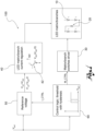
Figure 1 is a block diagram of a driver circuit not covered by the scope of the invention; -
Figure 2 is a block diagram of the driver circuit according to the invention; -
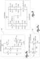
Figures 3-3d are a circuit implementation of the functional blocks of the block diagram infigure 2 ; -
Figure 4 shows the matrix of LEDs infigure 3 , in the parallel configuration; -
Figure 5 shows the matrix of LEDs infigure 3 , in the serial configuration; -
Figures 6 and 6a are a circuit diagram of another matrix of LEDs according to the invention; -
Figures 7 is a circuit diagram of another matrix of LEDs according to the invention; -
Figure 7a is a table of the states of the control signals for the matrix infigure 7 ; and -
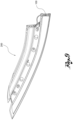
Figure 8 is an example of a vehicle light in which the LEDs are driven by a driver circuit according to the invention. - In the following description, the term "connected" refers both to a direct electrical connection between two circuit elements and to an indirect connection by means of one or more active or passive intermediate elements. The term "circuit" may indicate either a single component or a plurality of components, active/or passive, connected to each other to achieve a predefined function. Moreover, where a bipolar junction transistor (BJT) or a field effect transistor (FET) can be used, the meaning of the terms "base", "collector", "emitter", comprise the terms "gate", "drain" and "source" and vice versa. Except as otherwise indicated, lastly, NPN type transistors may be used in place of PNP transistors and vice versa.
- The driver circuit of lighting sources according to the invention, globally denoted by
reference numeral 100; 100', will now be described with reference to the block diagrams infigures 1 and2 . - In said block diagrams, as also in the circuit diagrams below, the LEDs have been indicated as examples of possible lighting sources.
- The circuit comprises a power supply terminal which can be connected to a direct voltage power supply generator (Vbat). Said power supply terminal powers a plurality of
LEDs 10 positioned on one or more lighting branches. It is to be noted that the invention is equally applicable to both a matrix configuration of LEDs and to the case of LEDs in a single source/multi-source configuration. - In the continuation of the description, an LED matrix is understood to mean a plurality of LEDs connected in a matrix, that is to say positioned in rows, wherein the LEDs of each row are connected in parallel with each other. The matrix of LEDs may be driven by a lighting switch and is therefore subject to a potential difference between the power supply terminal and a terminal of the lighting switch.
- A single source/multi-source configuration is understood to mean a plurality of LEDs positioned on several lighting branches connected in parallel to each other, wherein each of such may be driven by a respective lighting switch and is therefore subject to a potential difference between the power supply terminal and a terminal of the lighting switch, as may be clearly deduced from the description below. The LEDs of each lighting branch are connected in series with each other.
- As mentioned above, in the continuation of the description, the term "parallel" is used not just to indicate a connection in parallel of electric components according to the known definition of electrical engineering, but also to indicate lighting branches or columns of matrices of LEDs placed between the power supply terminal and the lighting switch terminal/s.
- As mentioned above, moreover, in the continuation of the description, a lighting "branch" will be understood as one or more lighting sources connected in series with each other or belonging to the same column of an LED matrix. Branch current (ILED) is consequently understood to mean the current crossing the lighting sources of a lighting branch. A driver current (IDRIVER) instead is understood to mean the current imposed by a lighting switch placed in cascade with a lighting branch or a matrix of LEDs. Power supply current is, lastly, understood to mean the overall current supplied by the driver circuit to power all the light sources and, therefore, all the lighting branches.
- The circuit comprises switching means 20 which can be operated to modify the path of the overall power supply electric current crossing said lighting sources. Said switching means 20 can be operated to switch the path of the overall power supply electric current between at least one first path, corresponding to a first circuit configuration, or "parallel" configuration of the interconnections between the lighting sources, and at least one second path, corresponding to a second circuit configuration, or "serial" configuration of the interconnections between the lighting sources.
- The lighting sources are positioned on one or more lighting branches, according to the definition of lighting branch given above, and said at least two circuit configurations have a different number of lighting branches.
- The switching means 20 can be operated to modify the path of the current crossing the lighting sources depending on the direct voltage power supply value.
- In other words, the switching means 20 permit the configuration of the lighting branches to be modified so as to reduce or increase the number thereof depending on the power supply voltage, on the basis of a comparison of circuit signals, as will be specified below, keeping the number of lighting sources constant. In particular, for low values of the power supply voltage, the switching means are activated to determine the path for the power supply current of the lighting sources which entails an increase in the number of lighting branches, and consequently a reduction of the number of lighting sources for each branch. Having reduced the number of lighting sources of each branch, said lighting sources may be correctly powered even by a low power supply voltage.
- Vice versa, in the case of high power supply voltage values, the switching means are activated to determine a different path of the power supply current, which entails a reduction in the number of lighting branches, and consequently an increase in the number of lighting sources for each branch. The branch current being determined solely by the current imposed on the lighting sources, to obtain the desired luminosity, reducing the number of such branches therefore means reducing the total power supply current required by the driver circuit and therefore the absorbed power.
- In the continuation of the description, "serial configuration" will be taken to generally mean a configuration of the lighting branches which presents a smaller number of lighting branches compared to a "parallel configuration" which indicates instead a configuration of the lighting branches with a greater number of lighting branches.
- As described in more detail below, the switching means 20 can be operated to connect at least two lighting branches alternately in parallel or in series. Passing from the parallel configuration to the serial configuration therefore means reducing the number of lighting branches; passing, vice versa, from the serial configuration to the parallel configuration means increasing the number of lighting branches.
- In one embodiment with at least three lighting branches, the switching means 20 can be operated to connect the
lighting sources 10 of a lighting branch of a first configuration, or parallel configuration, respectively to further lighting branches of said first configuration, so as to obtain a second configuration, or series configuration, having a reduced number of lighting branches, and vice versa. In this case, therefore starting for example from a parallel configuration with three lighting branches, one may pass to a serial configuration with two lighting branches connecting some of the lighting sources of a first branch in series to the lighting sources of a second branch and the remaining lighting sources of the first branch in series to the sources of the third branch. This way, in the serial configuration, the first lighting branch disappears and there is a power saving of 33%. - The switching means 20 are commanded by the "Matrix/branch driver switches" 30 which comprise command circuit means, such as transistors, suitable for activating the switching means 20 in the presence of a control signal M_CTRL.
- Returning to the block diagram, the lighting branches are powered by means of the "LED matrix/branch current regulation"
block 40. Said block contains in other words, circuit means suitable for imposing in the lighting branches a branch current ILED required by the lighting sources to provide the desired luminosity, preferably a constant current in the case of a current stabilised driver circuit. Said circuit means comprise at least onelighting switch 42 connected at least to a respective lighting branch which can be operated to impose a driver current IDRIVER which translates into a constant branch current ILED through said lighting branch. Preferably, said driver current is dependent on a driver voltage (Vref) applied to thelighting switch 42. - In a preferred embodiment, said
lighting switch 42 is a transistor. - As mentioned above, to obtain the benefits offered by the invention, the branch current circulating in the single lighting branch must remain the same both in the serial configuration and in the parallel configuration, regardless of the number of branches and of the number of lighting sources in each branch. In the case illustrated of a current stabilised driver circuit, the branch current is also constant. Since in the case of a parallel configuration of the lighting branches there is a greater absorption of overall current than in the serial configuration, the number of branches being greater, the driver current generated by the power supply switch must be greater in the case of a parallel configuration.
- Consequently, the circuit also comprises a "Voltage reference"
block 50, including driver voltage regulation means suitable for regulating the value of the driver voltage Vref depending on the serial or parallel configuration of the lighting branches, so as to vary the driver current IDRIVER to keep the branch current ILED constant as said configuration varies. - The circuit further comprises a "Control logic"
block 60, which includes control means suitable for providing the "Matrix/branch switches driver" 30 with the matrix control signal M_CTRL and the "Voltage reference"block 50 with a current control signal I_CTRL to switch the value of the driver voltage to apply to the lighting switch/switches. - In the embodiment shown in
figure 1 , which is not part of the invention, said control means are suitable for comparing the power supply voltage with a predefined threshold value. For example, said predefined threshold value is related to the product of the number of LEDs on the lighting branches and the junction voltage of each LED, bearing in mind a safety margin and applying an appropriate hysteresis. Consequently, when switching from the parallel configuration to the serial configuration is required, the number of LEDs on the lighting branches in the serial configuration is considered and, when the power supply voltage increases as far as exceeding the upper predefined threshold value, the "Control logic" block commands the "Reference voltage" block to reduce the driver voltage and commands the "Matrix/branch switches driver" to switch the switching means into the serial configuration. - Vice versa, when the power supply voltage is in the phase of decreasing from the nominal value, and switching from the serial configuration to the parallel configuration is therefore required, the previously defined threshold value is considered and, when the power supply voltage falls below the lower predefined threshold value, the "Control logic" block commands the "Reference voltage" block to increase the driver voltage and commands the "Matrix/branch switches driver" to switch the switching means into the parallel configuration.
- It is evident that the lower the threshold value the better in that switching to the reduced consumption serial configuration takes place earlier.
- Rather than using a predefined threshold value, according to the invention, the circuit 100' uses an adaptive threshold (
Figure 2 ) obtained by monitoring the effective state of the driver circuit. In particular, the control means get the information needed to calculate the adaptive threshold from the "LED matrix/branch current regulation"block 40. As will be described further below, the control means are suitable for detecting the voltage drop at the terminals of at least one of the lighting switches 42 connected in cascade to the respective lighting branch/branches (the collector and emitter terminals in the case of lighting transistor) and to command the switch means and the driver voltage regulation means to pass from the series configuration to the parallel configuration when said voltage falls below a predefined threshold value. In this condition, in fact, the lighting transistor is about to pass from the linear zone to the saturation zone and will therefore no longer be able to regulate the current needed to turn on the lighting sources; it is therefore necessary to switch to the parallel configuration. - The control means are also suitable for comparing the voltage drop at the terminals of at least one of the lighting switches 42 connected in cascade to the respective lighting branch/branches with the voltage drop at the ends of the respective lighting sources and to command the switching means and the driver voltage regulation means to pass from the parallel configuration to the serial configuration, depending on such comparison.
- A first practical example of implementation of the block diagram in
figure 2 , that is to say with the adaptive threshold, will now be described with reference to the circuit implementation offigures 3-3d . - In the example shown, said driver circuit is suitable for driving an LED matrix comprising 8 LEDs. According to the invention, said LED matrix may switch from a parallel configuration, in which it is formed of two rows and four columns of LEDs (from left to right: D10,D11; D1,D2; D6,D3; D13,D12) and a serial configuration, in which it is formed of four rows and two columns.
- The LED matrix is connected between a power supply terminal VDD and the collector COLLECTOR of a lighting transistor Q1, which is part of the "Matrix current regulation"
block 40. - The switching means comprise a first switching transistor Q10, connected between the third and fourth column of LEDs and the collector of the lighting transistor, a second switching transistor Q16, connected between the power supply terminal VDD and the first two columns of LEDs, and a diode, preferably a Schottky diode, connected between the cathodes of the third and fourth column of LEDs and the anodes of the first and second column of LEDs.
- A starting situation in which both switching transistors Q10 and Q16 are on (
figure 4 ) is considered. The four lighting branches are all in parallel with each other (if one ignores the VCE,SAT of the two switching transistors). - As soon as the switching transistors Q10 and Q16 are turned off, the collector voltage of the lighting transistor Q1 drops, in that said lighting transistor tries to keep the driver current constant and therefore lowers its resistivity between its collector and emitter terminals. As the collector voltage drops, the voltage at the ends of the LEDs of the first two columns (D1,D10,D2,D11) drops too, while the voltage at the anodes of the third and fourth columns remain constrained to VDD. This condition leads the switching diode D4 to be polarised in the direct zone and start conducting.
- After a brief transition, in which the luminosity drops but not visibly to the human eye, the matrix consequently moves into the "serial" configuration, that is of 4
rows X 2 columns (figure 5 ). - In the inverse process, the switching transistors Q10 and Q16 turn on and constrain the anodes of the LEDs of the first two columns (D10, D1, D11, D2) to the voltage of the power supply terminal VDD; in the same way, the cathodes of the LEDs of the third and fourth column (D6,D13,D3,D12) are constrained to the voltage of the collector terminal COLLECTOR. As a result, the switching diode D4 turns off.
- Moving on to the "Matrix current regulation"
block 40, the lighting transistor Q1 is connected to a first operational amplifier U1 which imposes on the emitter EMITTER of the lighting transistor Q1, connected to the earth by the resistor R5, the driver voltage Vref'=2Vx or Vref"=Vx generated by the "Voltage reference"block 50, and, in particular, present on the output of a second operational amplifier U2 belonging to such block, the voltage Vx being, as will be explained below, a non-inverting input voltage of said second operational amplifier U2. This way, the driver current which runs through the LED matrix is known and stabilised. - The operational amplifiers U1 and U2 are used in feedback. So, the first operational amplifier U1 takes back the driver voltage Vref', Vref", which it has on its non-inverting input (+), on its inverting input (-), and therefore on the emitter EMITTER of the lighting transistor Q1.
- The "Voltage reference"
block 50 comprises a zener diode D7 powered with a constant current. The voltage Vz at the ends of the zener diode D7 is therefore constant, regardless of the power supply voltage. A first stabilised voltage Vop used, for example, to power the operational amplifiers derives from said voltage Vz through the transistor Q2. Moreover, a second voltage Vx, which enters the non-inverting input of the second operational amplifier U2 in a constant manner, derives from the voltage Vz through the voltage divider R1, R18. The second operational amplifier U2 generates the driver voltage Vref'=2Vx, or Vref"=Vx, on its output, depending on the configuration of the feedback loop R21, R35, determined by the current control signal I_CTRL coming from the "Control logic"block 60. - The terminal relative to said signal I_CTRL is connected to the collector of the transistor Q18 of the "Control logic"
block 60. Said transistor Q18 works either on in saturation or off. When it is in saturation, its VCE,SAT may be considered almost null and the configuration of non-inverting amplifier is obtained for the second operational amplifier U2, with gain determined by the resistors R35, R21, in this case equal to 2. - When, instead, Q18 is off, the resistor R21 no longer counts and one has a follower configuration, achieving in output at the second operational amplifier Vref"=Vx.
- The transistor Q18 is in turn commanded by a control signal STATUS which indicates in what state the LED matrix is, that is to say, in the serial configuration or in the parallel configuration.
- Where said STATUS control signal comes from a
bistable circuit 62, suitable for holding in its memory the state of the matrix of LEDs, as well as turning on and off the transistor Q18, the STATUS output of thebistable circuit 62 causes the turning on or off of another transistor Q7 of the "Control logic "block 60, suitable for generating the matrix control signal M_CTRL which, by means of the "Matrix switches driver"block 30, commands the transistors Q10 and Q16. - In the
bistable circuit 62, the output signal is switched by the input signals status TO_LOWER and TO_UPPER, generated by respectivedifferential circuits differential circuits - The differential
lower threshold circuit 64 defines a lower threshold voltage VTHL as:

where VEQ1 is the voltage on the emitter EMITTER terminal of the lighting transistor Q1 and where VBEQ1 is the voltage difference between the base terminal BASE and the emitter terminal EMITTER of said lighting transistor. - So, according to the differential circuit, if VCQ1 < VTHL, then the output signal TO_LOWER is activated, inasmuch as crossed by current, and makes the bistable 62 and thereby the matrix of LEDs, change status.
- The upper
differential threshold circuit 66 defines an upper threshold voltage VTHH as:

where VDD is the voltage at the power supply terminal. - So, according to the differential circuit, if VCQ1 > VTHH, then the output signal TO_UPPER is activated, inasmuch as crossed by current, and makes the bistable and thereby the matrix, change status.
- In the case of the lower threshold
differential circuit 64, the circuit realises that the lighting transistor Q1 is approaching saturation and that upon further lowering of the power supply voltage, such transistor will be unable to keep the LEDS on. It is therefore necessary to pass from the serial configuration to the parallel configuration. In practice, therefore, the lower thresholddifferential circuit 64 performs a comparison between the base voltage and the collector voltage of the lighting transistor. - As regards the upper threshold
differential circuit 66, the passage from the parallel configuration to the serial configuration occurs when the voltage between the collector and emitter of the lighting transistor Q1 (plus a certain margin given by the drop on the elements making the matrix switch, plus a certain hysteresis with regard to the lower threshold VTHL) is almost equal to the drop on the lighting branch (VDD-VCQ1). In fact, passing from the parallel configuration to the serial configuration, the voltage drop on the lighting branches doubles, in that the matrix of LEDs passes from 2 to 4 rows. If there is an additional voltage drop between the collector and emitter of the lighting transistor Q1, this means that the matrix of LEDs can pass from the parallel configuration to the serial configuration. - In other words, in this condition, the lighting transistor Q1 may "surrender" its VCE to the matrix in serial configuration, without going into saturation.
- In another embodiment, shown in
figures 6 and 6a , the LED matrix infigure 6 comprises six LEDs and is able to switch between a parallel configuration of 2 rows by 3 columns, and a serial configuration of 3 rows by 2 columns, depending on the status of the switching transistors Q4, Q10 and Q16.Figure 6 also shows the "Matrix switches driver" for the control of the switching transistors of the matrix of LEDs infigure 6 . The remaining blocks of the driver circuit do not differ compared to the same blocks described above for the case of the 2-4 matrix of LEDs. As may be seen from the arrows infigure 6 , showing the paths of the current in the two circuit configurations of use of the matrix, in a first configuration, which may be defined parallel, the matrix has three lighting branches, respectively comprising the pairs of LEDs D14,D15; D10,D12; and D13,D11. Such first configuration is obtained by turning on all the switching transistors Q4, Q10 and Q16 and with the switching diodes D1 and D4 denied access. In the second configuration, which may be defined serial, the matrix has two lighting branches, respectively comprising the LEDs D14, D13, D15 and D10, D12, D11. Such second configuration is obtained by turning off all three switching transistors and with the diodes D1 and D4 conducting. It is to be noted that in this case the two driver voltages are Vref'=Vx*3/2 and Vref"=Vx. - In another embodiment, shown in
figures 7-7d , the driver circuit has lighting branches in a matrix configuration. In particular, two lighting transistors are used, Q1 and Q19, each connected to a plurality of lighting sources according to the two "parallel-serial" configurations described now. The switching means comprise two switching transistors Q4 and Q10 and two switching diodes D1 and D4. - In a first configuration, which may be defined parallel, shown in
Figure 7c , the two switching transistors Q4 and Q10 are on and the two switching diodes D4 and D1 are denied access. In this state of the switching means, the driver circuit presents a matrix of LEDs of two rows and two columns (LED D14, D10 and D15, D11), to which a first lighting transistor Q19 is connected, and a matrix of LEDs of one row and two columns (LED D13,D12), to which a second lighting transistor Q1 is connected, In practice, therefore in this parallel configuration, there are four lighting branches according to the definition given above of lighting branch. - In a second configuration, which may be defined a serial configuration, shown in
Figure 7d , the two switching transistors Q4 and Q10 are off and the two switching diodes D4 and D1 are directly polarised, that is to say conducting. In this state of the switching means, the driver circuit presents a matrix of LEDs of three rows and two columns, to which the collectors of both lighting transistors Q19 and Q1 are connected, connected to each other by the switching diode D1. In practice, therefore in this parallel configuration, there are two lighting branches according to the definition given above of lighting branch. -
Figures 7a and 7b show a circuit implementation of the "Matrix current regulation" block, in this case comprising the two lighting transistors Q1 and Q19 and the "Matrix switches driver" for the control of the two switching transistors of the matrix of LEDs infigure 7 . The remaining blocks of the driver circuit do not differ compared to the same blocks described above for the case of the 2-4 matrix of LEDs. - In a further embodiment, shown in
figures 8, 8a , two 2 x 3 matrices, as shown infigure 6 , are connected between the power supply terminal VDD and the collector of alighting transistor 42, as shown infigure 8 . Depending on the status of the control signal M_CTRL_1, these matrices may pass from a two row configuration of LEDs per lighting branch, to a status of three rows of LEDs per lighting branch. Depending on the status of the control signal M_CTRL_2, rather, the two matrices may be connected in series or in parallel to each other. The combined effect of changing the status of the signals M_CTRL_1 and M_CTRL_2 therefore permits four different circuit combinations to be obtained, as described in the table infigure 8a , with a number of rows of LEDs per lighting branch which may be equal to 2, 3, 4 or 6. These four configurations or levels, are separated by three thresholds. In the passage from one configuration to another, at each increase in the number of rows of LEDs per lighting branch, there is a respective drop in the number of columns, to the benefit of a saving of the absorbed power. - In an embodiment not covered by the invention, for example, the reference voltage Vx is not constant but depends on the power supply voltage VDD, according to the relation

- An example of such driver circuit is described in the patent application
PD2011A000371 - In this case, in the circuit implementation shown in
figures 3-3d we will have, simply

- With reference to
figure 9 , the present invention relates to avehicle light 200 wherein at least one light of the vehicle light is made with LED light sources driven by the driver circuit of the invention described above. Thevehicle light 200 may be a front, rear or brake light of the vehicle and, for example, a light of the rear light may be a sidelight, brake light or fog light. - A person skilled in the art may make modifications and adaptations to the embodiments of the driver circuit according to the invention, replacing elements with others functionally equivalent so as to satisfy contingent requirements while remaining within the scope of protection of the following claims.
- For example, the control circuit means may be implemented in a software, for example, using a micro controller processing unit or a DSP, to obtain the control signal as described above.
Claims (5)
- Driver circuit for powering a plurality of light sources (10) with an overall power supply electric current, wherein the plurality of light sources (10) is arranged in a plurality of lighting branches connected in parallel with each other, where each lighting branch comprises light sources of the plurality of light sources (10) connected in series to each other, comprising:- switching means (20) configured to switch the path of the overall power supply electric current between at least one first path, corresponding to a first circuit configuration of the interconnections between the light sources (10), and at least one second path, corresponding to a second circuit configuration of the interconnections between the light sources (10), wherein said first and second circuit configurations have a different number of lighting branches;- at least one lighting switch (42) connected in cascade to at least one respective lighting branch and configured to impose a branch current (ILED) through said at least one respective lighting branch required by the light sources to provide the desired luminosity, the branch current depending on a driver voltage (Vref) applied to said at least one lighting switch (42);- driver voltage regulation means (50), configured to regulate the driver voltage value according to the first or second circuit configuration of the plurality of lighting branches so as to maintain the branch current (ILED) unchanged as said circuit configuration varies; and- control means (60) configured to command the switching means (20) and the driver voltage regulation means (50) to pass from the first circuit configuration being a parallel configuration of the light sources of a lighting branch with the light sources of the other lighting branches of the plurality of lighting branches, to the second circuit configuration, being a series configuration of the light sources of a lighting branch with the light sources of the other lighting branches of the plurality of lighting branches, and vice versa, the driver circuit being characterised in that the control means (60) are further configured to:- detect the voltage drop at the terminals of the at least one lighting switch (42) and to command the switching means (20) and the driver voltage regulation means (50) to pass from the second circuit configuration to the first circuit configuration when said voltage drop falls below a predefined threshold value,- compare the voltage drop at the terminals of the at least one lighting switch (42) connected in cascade to the at least one respective lighting branch with the voltage drop at the ends of said at least one respective lighting branch and to command the switching means (20) and the driver voltage regulation means (50) to pass from the first circuit configuration to the second circuit configuration, depending on such comparison.
- Driver circuit according to claim 1, wherein the light sources (10) are connected to a power supply terminal (VDD) adapted to be connected to a direct voltage power supply generator (Vbat).
- Driver circuit according to claim 1, wherein said driver voltage (Vref) is configured to drive the at least one lighting switch (42).
- Driver circuit according to any of the previous claims, wherein said switching means (20) comprise switching transistors (Q10, Q16) which, when in a conductive state, are configured to connect the lighting branches in the first circuit configuration and at least one switch diode element (D4) which when said switching transistors are in a cut-off state, is configured to connect the plurality of lighting branches in the second circuit configuration.
- Vehicle light, characterised by comprising a driver circuit according to any of the claims from 1 to 4.
Applications Claiming Priority (1)
| Application Number | Priority Date | Filing Date | Title |
|---|---|---|---|
| IT000025A ITPD20120025A1 (en) | 2012-02-01 | 2012-02-01 | LED PILOT CIRCUIT, PILOT METHOD AND AUTOMOTIVE HEADLAMP |
Publications (3)
| Publication Number | Publication Date |
|---|---|
| EP2624662A2 EP2624662A2 (en) | 2013-08-07 |
| EP2624662A3 EP2624662A3 (en) | 2017-05-03 |
| EP2624662B1 true EP2624662B1 (en) | 2024-11-27 |
Family
ID=46000110
Family Applications (1)
| Application Number | Title | Priority Date | Filing Date |
|---|---|---|---|
| EP13153314.3A Active EP2624662B1 (en) | 2012-02-01 | 2013-01-30 | Led driver circuit, method of driving and vehicle light |
Country Status (4)
| Country | Link |
|---|---|
| US (1) | US9769891B2 (en) |
| EP (1) | EP2624662B1 (en) |
| CN (1) | CN103249218B (en) |
| IT (1) | ITPD20120025A1 (en) |
Families Citing this family (8)
| Publication number | Priority date | Publication date | Assignee | Title |
|---|---|---|---|---|
| PL2947965T3 (en) * | 2014-05-23 | 2017-08-31 | Automotive Lighting Italia S.P.A. A Socio Unico | Driver device for light sources |
| FR3025395B1 (en) * | 2014-08-26 | 2019-06-28 | Commissariat A L'energie Atomique Et Aux Energies Alternatives | LED LIGHTING DEVICE |
| FR3035768B1 (en) * | 2015-04-29 | 2018-06-29 | Valeo Vision | LUMINOUS DEVICE PROVIDING MULTIPLE LIGHT FUNCTIONS OF A MOTOR VEHICLE USING LIGHT SOURCE GROUPS DEDICATED BY FUNCTION |
| US10111287B2 (en) * | 2015-09-15 | 2018-10-23 | Semiconductor Components Industries, Llc | Synchronous switching circuit |
| US9713210B2 (en) | 2015-09-15 | 2017-07-18 | Semiconductor Components Industries, Llc | LED lighting system |
| JP6720753B2 (en) * | 2016-07-27 | 2020-07-08 | 東芝ライテック株式会社 | Vehicle lighting device and vehicle lamp |
| JP6922578B2 (en) | 2017-09-13 | 2021-08-18 | 東芝ライテック株式会社 | Vehicle lighting and vehicle lighting |
| TWI794947B (en) * | 2021-08-26 | 2023-03-01 | 眾用車材製造股份有限公司 | The method of controlling the warning light to enter the low power mode |
Citations (3)
| Publication number | Priority date | Publication date | Assignee | Title |
|---|---|---|---|---|
| DE9313820U1 (en) * | 1993-09-13 | 1994-01-20 | Gebensleben, Enno, 22547 Hamburg | Bicycle lights |
| US20110095704A1 (en) * | 2009-10-26 | 2011-04-28 | Light-Based Technologies Incorporated | Power supplies for led light fixtures |
| EP2319276B1 (en) * | 2008-07-29 | 2011-11-16 | Koninklijke Philips Electronics N.V. | Illumination device comprising multiple leds |
Family Cites Families (13)
| Publication number | Priority date | Publication date | Assignee | Title |
|---|---|---|---|---|
| DE102006024607A1 (en) * | 2006-05-26 | 2007-11-29 | Bayerische Motoren Werke Ag | Light system for motor vehicle, has two branches, where one branch is parallelly connected or adjustable to other branch, where bridge section is provided for adjustably connecting of two branches |
| EP2996441B1 (en) * | 2008-03-17 | 2020-12-16 | eldoLAB Holding B.V. | Led fixture and led assembly |
| CN102113410B (en) * | 2008-07-29 | 2013-11-06 | 皇家飞利浦电子股份有限公司 | Illumination device comprising multiple leds |
| US7994725B2 (en) * | 2008-11-06 | 2011-08-09 | Osram Sylvania Inc. | Floating switch controlling LED array segment |
| EP2214456A1 (en) * | 2009-01-22 | 2010-08-04 | Nanker(Guang Zhou)Semiconductor Manufacturing Corp. | LED lamp circuit |
| TW201105172A (en) * | 2009-07-30 | 2011-02-01 | Advanced Connectek Inc | Light emitting diode (LED) device and driving method thereof |
| EP2836054B1 (en) * | 2009-08-18 | 2020-10-14 | eldoLAB Holding B.V. | Control unit for a LED assembly and lighting system |
| WO2011077909A1 (en) * | 2009-12-22 | 2011-06-30 | シチズンホールディングス株式会社 | Led drive circuit |
| EP2533307B1 (en) | 2010-02-03 | 2015-04-08 | Citizen Holdings Co., Ltd. | Led drive circuit |
| US8569974B2 (en) * | 2010-11-01 | 2013-10-29 | Cree, Inc. | Systems and methods for controlling solid state lighting devices and lighting apparatus incorporating such systems and/or methods |
| CN102752899B (en) * | 2011-04-02 | 2015-11-25 | 英飞特电子(杭州)股份有限公司 | A kind of circuit adjusting LED current |
| US8853958B2 (en) * | 2011-11-22 | 2014-10-07 | Cree, Inc. | Driving circuits for solid-state lighting apparatus with high voltage LED components and related methods |
| ITPD20110371A1 (en) | 2011-11-23 | 2013-05-24 | Automotive Lighting Italia S P A A Socio Unico | LED PILOT CIRCUIT, PILOT METHOD AND AUTOMOTIVE HEADLAMP |
-
2012
- 2012-02-01 IT IT000025A patent/ITPD20120025A1/en unknown
-
2013
- 2013-01-30 EP EP13153314.3A patent/EP2624662B1/en active Active
- 2013-02-01 US US13/757,492 patent/US9769891B2/en active Active
- 2013-02-01 CN CN201310042461.0A patent/CN103249218B/en active Active
Patent Citations (3)
| Publication number | Priority date | Publication date | Assignee | Title |
|---|---|---|---|---|
| DE9313820U1 (en) * | 1993-09-13 | 1994-01-20 | Gebensleben, Enno, 22547 Hamburg | Bicycle lights |
| EP2319276B1 (en) * | 2008-07-29 | 2011-11-16 | Koninklijke Philips Electronics N.V. | Illumination device comprising multiple leds |
| US20110095704A1 (en) * | 2009-10-26 | 2011-04-28 | Light-Based Technologies Incorporated | Power supplies for led light fixtures |
Also Published As
| Publication number | Publication date |
|---|---|
| EP2624662A2 (en) | 2013-08-07 |
| US20140021860A1 (en) | 2014-01-23 |
| CN103249218A (en) | 2013-08-14 |
| CN103249218B (en) | 2018-08-03 |
| ITPD20120025A1 (en) | 2013-08-02 |
| EP2624662A3 (en) | 2017-05-03 |
| US9769891B2 (en) | 2017-09-19 |
Similar Documents
| Publication | Publication Date | Title |
|---|---|---|
| US9769891B2 (en) | LED driver circuit, method of driving and vehicle light | |
| CN100405245C (en) | Closed-loop current control circuit and method thereof | |
| US11477871B2 (en) | Lighting circuit of automotive lamp | |
| US20110148323A1 (en) | Control of multi-string led array | |
| KR101967950B1 (en) | Multi-channel LED driver with overheat protection capabilities | |
| KR102761833B1 (en) | Light emitting diode driver for load changes | |
| JP2014170880A (en) | Light-emitting element switch-on device and light source device | |
| US10383185B2 (en) | Motor vehicle illumination device | |
| CN104798306B (en) | Device for controlling a field effect transistor | |
| JP2019057420A (en) | Light source control unit and vehicle lamp | |
| EP2749132B1 (en) | Led driver circuit, driving method and vehicle light | |
| US9307594B2 (en) | Apparatus for driving light emitting diode having a current switch | |
| EP2750476A1 (en) | Driver circuit of light sources and vehicle light provided with said driver circuit of light sources | |
| WO2023097578A1 (en) | Light source driver | |
| US20220039236A1 (en) | Transient suppression systems and methods in electrical circuits | |
| KR20140100392A (en) | LED illumination device involving led-working groups | |
| JP2021535543A (en) | LED drive circuit | |
| KR102804560B1 (en) | LED Driver for Operating at Low Voltage | |
| JP2023515816A (en) | LED lighting system and control method | |
| KR102581457B1 (en) | Apparatus of driving a light source and method thereof | |
| Kraft | Convert a Buck Regulator into a Smart LED Driver, Including Dimming | |
| KR20140136210A (en) | LED illumination device for preventing flicker | |
| KR20200087374A (en) | Circuit for regulating intensity of light in LED(Light Emitting Diode) and method thereof | |
| KR20150010180A (en) | LED illumination device involving led-working groups | |
| KR20150010177A (en) | LED illumination device involving led-working groups |
Legal Events
| Date | Code | Title | Description |
|---|---|---|---|
| PUAI | Public reference made under article 153(3) epc to a published international application that has entered the european phase |
Free format text: ORIGINAL CODE: 0009012 |
|
| AK | Designated contracting states |
Kind code of ref document: A2 Designated state(s): AL AT BE BG CH CY CZ DE DK EE ES FI FR GB GR HR HU IE IS IT LI LT LU LV MC MK MT NL NO PL PT RO RS SE SI SK SM TR |
|
| AX | Request for extension of the european patent |
Extension state: BA ME |
|
| PUAL | Search report despatched |
Free format text: ORIGINAL CODE: 0009013 |
|
| AK | Designated contracting states |
Kind code of ref document: A3 Designated state(s): AL AT BE BG CH CY CZ DE DK EE ES FI FR GB GR HR HU IE IS IT LI LT LU LV MC MK MT NL NO PL PT RO RS SE SI SK SM TR |
|
| AX | Request for extension of the european patent |
Extension state: BA ME |
|
| RIC1 | Information provided on ipc code assigned before grant |
Ipc: H05B 33/08 20060101AFI20170327BHEP |
|
| STAA | Information on the status of an ep patent application or granted ep patent |
Free format text: STATUS: REQUEST FOR EXAMINATION WAS MADE |
|
| 17P | Request for examination filed |
Effective date: 20171102 |
|
| RBV | Designated contracting states (corrected) |
Designated state(s): AL AT BE BG CH CY CZ DE DK EE ES FI FR GB GR HR HU IE IS IT LI LT LU LV MC MK MT NL NO PL PT RO RS SE SI SK SM TR |
|
| STAA | Information on the status of an ep patent application or granted ep patent |
Free format text: STATUS: EXAMINATION IS IN PROGRESS |
|
| 17Q | First examination report despatched |
Effective date: 20180329 |
|
| RAP1 | Party data changed (applicant data changed or rights of an application transferred) |
Owner name: MARELLI AUTOMOTIVE LIGHTING ITALY S.P.A. |
|
| P01 | Opt-out of the competence of the unified patent court (upc) registered |
Effective date: 20230526 |
|
| REG | Reference to a national code |
Ref country code: DE Ref legal event code: R079 Free format text: PREVIOUS MAIN CLASS: H05B0033080000 Ipc: H05B0045100000 Ref country code: DE Ref legal event code: R079 Ref document number: 602013086320 Country of ref document: DE Free format text: PREVIOUS MAIN CLASS: H05B0033080000 Ipc: H05B0045100000 |
|
| GRAP | Despatch of communication of intention to grant a patent |
Free format text: ORIGINAL CODE: EPIDOSNIGR1 |
|
| STAA | Information on the status of an ep patent application or granted ep patent |
Free format text: STATUS: GRANT OF PATENT IS INTENDED |
|
| RIC1 | Information provided on ipc code assigned before grant |
Ipc: H05B 45/46 20200101ALI20240611BHEP Ipc: H05B 45/48 20200101ALI20240611BHEP Ipc: H05B 45/14 20200101ALI20240611BHEP Ipc: H05B 45/44 20200101ALI20240611BHEP Ipc: H05B 45/10 20200101AFI20240611BHEP |
|
| INTG | Intention to grant announced |
Effective date: 20240703 |
|
| GRAS | Grant fee paid |
Free format text: ORIGINAL CODE: EPIDOSNIGR3 |
|
| GRAA | (expected) grant |
Free format text: ORIGINAL CODE: 0009210 |
|
| STAA | Information on the status of an ep patent application or granted ep patent |
Free format text: STATUS: THE PATENT HAS BEEN GRANTED |
|
| AK | Designated contracting states |
Kind code of ref document: B1 Designated state(s): AL AT BE BG CH CY CZ DE DK EE ES FI FR GB GR HR HU IE IS IT LI LT LU LV MC MK MT NL NO PL PT RO RS SE SI SK SM TR |
|
| REG | Reference to a national code |
Ref country code: GB Ref legal event code: FG4D |
|
| REG | Reference to a national code |
Ref country code: CH Ref legal event code: EP |
|
| REG | Reference to a national code |
Ref country code: IE Ref legal event code: FG4D |
|
| REG | Reference to a national code |
Ref country code: DE Ref legal event code: R096 Ref document number: 602013086320 Country of ref document: DE |
|
| REG | Reference to a national code |
Ref country code: LT Ref legal event code: MG9D |
|
| REG | Reference to a national code |
Ref country code: NL Ref legal event code: MP Effective date: 20241127 |
|
| PG25 | Lapsed in a contracting state [announced via postgrant information from national office to epo] |
Ref country code: HR Free format text: LAPSE BECAUSE OF FAILURE TO SUBMIT A TRANSLATION OF THE DESCRIPTION OR TO PAY THE FEE WITHIN THE PRESCRIBED TIME-LIMIT Effective date: 20241127 Ref country code: PT Free format text: LAPSE BECAUSE OF FAILURE TO SUBMIT A TRANSLATION OF THE DESCRIPTION OR TO PAY THE FEE WITHIN THE PRESCRIBED TIME-LIMIT Effective date: 20250327 Ref country code: IS Free format text: LAPSE BECAUSE OF FAILURE TO SUBMIT A TRANSLATION OF THE DESCRIPTION OR TO PAY THE FEE WITHIN THE PRESCRIBED TIME-LIMIT Effective date: 20250327 |
|
| PG25 | Lapsed in a contracting state [announced via postgrant information from national office to epo] |
Ref country code: FI Free format text: LAPSE BECAUSE OF FAILURE TO SUBMIT A TRANSLATION OF THE DESCRIPTION OR TO PAY THE FEE WITHIN THE PRESCRIBED TIME-LIMIT Effective date: 20241127 Ref country code: NL Free format text: LAPSE BECAUSE OF FAILURE TO SUBMIT A TRANSLATION OF THE DESCRIPTION OR TO PAY THE FEE WITHIN THE PRESCRIBED TIME-LIMIT Effective date: 20241127 |
|
| REG | Reference to a national code |
Ref country code: AT Ref legal event code: MK05 Ref document number: 1747019 Country of ref document: AT Kind code of ref document: T Effective date: 20241127 |
|
| PG25 | Lapsed in a contracting state [announced via postgrant information from national office to epo] |
Ref country code: BG Free format text: LAPSE BECAUSE OF FAILURE TO SUBMIT A TRANSLATION OF THE DESCRIPTION OR TO PAY THE FEE WITHIN THE PRESCRIBED TIME-LIMIT Effective date: 20241127 |
|
| PG25 | Lapsed in a contracting state [announced via postgrant information from national office to epo] |
Ref country code: ES Free format text: LAPSE BECAUSE OF FAILURE TO SUBMIT A TRANSLATION OF THE DESCRIPTION OR TO PAY THE FEE WITHIN THE PRESCRIBED TIME-LIMIT Effective date: 20241127 |
|
| PG25 | Lapsed in a contracting state [announced via postgrant information from national office to epo] |
Ref country code: NO Free format text: LAPSE BECAUSE OF FAILURE TO SUBMIT A TRANSLATION OF THE DESCRIPTION OR TO PAY THE FEE WITHIN THE PRESCRIBED TIME-LIMIT Effective date: 20250227 |
|
| PG25 | Lapsed in a contracting state [announced via postgrant information from national office to epo] |
Ref country code: LV Free format text: LAPSE BECAUSE OF FAILURE TO SUBMIT A TRANSLATION OF THE DESCRIPTION OR TO PAY THE FEE WITHIN THE PRESCRIBED TIME-LIMIT Effective date: 20241127 Ref country code: GR Free format text: LAPSE BECAUSE OF FAILURE TO SUBMIT A TRANSLATION OF THE DESCRIPTION OR TO PAY THE FEE WITHIN THE PRESCRIBED TIME-LIMIT Effective date: 20250228 Ref country code: AT Free format text: LAPSE BECAUSE OF FAILURE TO SUBMIT A TRANSLATION OF THE DESCRIPTION OR TO PAY THE FEE WITHIN THE PRESCRIBED TIME-LIMIT Effective date: 20241127 |
|
| PG25 | Lapsed in a contracting state [announced via postgrant information from national office to epo] |
Ref country code: PL Free format text: LAPSE BECAUSE OF FAILURE TO SUBMIT A TRANSLATION OF THE DESCRIPTION OR TO PAY THE FEE WITHIN THE PRESCRIBED TIME-LIMIT Effective date: 20241127 |
|
| PG25 | Lapsed in a contracting state [announced via postgrant information from national office to epo] |
Ref country code: RS Free format text: LAPSE BECAUSE OF FAILURE TO SUBMIT A TRANSLATION OF THE DESCRIPTION OR TO PAY THE FEE WITHIN THE PRESCRIBED TIME-LIMIT Effective date: 20250227 |
|
| PG25 | Lapsed in a contracting state [announced via postgrant information from national office to epo] |
Ref country code: SM Free format text: LAPSE BECAUSE OF FAILURE TO SUBMIT A TRANSLATION OF THE DESCRIPTION OR TO PAY THE FEE WITHIN THE PRESCRIBED TIME-LIMIT Effective date: 20241127 |
|
| PG25 | Lapsed in a contracting state [announced via postgrant information from national office to epo] |
Ref country code: DK Free format text: LAPSE BECAUSE OF FAILURE TO SUBMIT A TRANSLATION OF THE DESCRIPTION OR TO PAY THE FEE WITHIN THE PRESCRIBED TIME-LIMIT Effective date: 20241127 |
|
| PG25 | Lapsed in a contracting state [announced via postgrant information from national office to epo] |
Ref country code: EE Free format text: LAPSE BECAUSE OF FAILURE TO SUBMIT A TRANSLATION OF THE DESCRIPTION OR TO PAY THE FEE WITHIN THE PRESCRIBED TIME-LIMIT Effective date: 20241127 |
|
| PG25 | Lapsed in a contracting state [announced via postgrant information from national office to epo] |
Ref country code: RO Free format text: LAPSE BECAUSE OF FAILURE TO SUBMIT A TRANSLATION OF THE DESCRIPTION OR TO PAY THE FEE WITHIN THE PRESCRIBED TIME-LIMIT Effective date: 20241127 |
|
| PG25 | Lapsed in a contracting state [announced via postgrant information from national office to epo] |
Ref country code: SK Free format text: LAPSE BECAUSE OF FAILURE TO SUBMIT A TRANSLATION OF THE DESCRIPTION OR TO PAY THE FEE WITHIN THE PRESCRIBED TIME-LIMIT Effective date: 20241127 |
|
| PG25 | Lapsed in a contracting state [announced via postgrant information from national office to epo] |
Ref country code: CZ Free format text: LAPSE BECAUSE OF FAILURE TO SUBMIT A TRANSLATION OF THE DESCRIPTION OR TO PAY THE FEE WITHIN THE PRESCRIBED TIME-LIMIT Effective date: 20241127 |
|
| REG | Reference to a national code |
Ref country code: DE Ref legal event code: R097 Ref document number: 602013086320 Country of ref document: DE |
|
| REG | Reference to a national code |
Ref country code: CH Ref legal event code: PL |
|
| PG25 | Lapsed in a contracting state [announced via postgrant information from national office to epo] |
Ref country code: SE Free format text: LAPSE BECAUSE OF FAILURE TO SUBMIT A TRANSLATION OF THE DESCRIPTION OR TO PAY THE FEE WITHIN THE PRESCRIBED TIME-LIMIT Effective date: 20241127 |
|
| PG25 | Lapsed in a contracting state [announced via postgrant information from national office to epo] |
Ref country code: MC Free format text: LAPSE BECAUSE OF FAILURE TO SUBMIT A TRANSLATION OF THE DESCRIPTION OR TO PAY THE FEE WITHIN THE PRESCRIBED TIME-LIMIT Effective date: 20241127 Ref country code: LU Free format text: LAPSE BECAUSE OF NON-PAYMENT OF DUE FEES Effective date: 20250130 |
|
| PLBE | No opposition filed within time limit |
Free format text: ORIGINAL CODE: 0009261 |
|
| STAA | Information on the status of an ep patent application or granted ep patent |
Free format text: STATUS: NO OPPOSITION FILED WITHIN TIME LIMIT |
|
| PG25 | Lapsed in a contracting state [announced via postgrant information from national office to epo] |
Ref country code: BE Free format text: LAPSE BECAUSE OF NON-PAYMENT OF DUE FEES Effective date: 20250131 |
|
| PG25 | Lapsed in a contracting state [announced via postgrant information from national office to epo] |
Ref country code: CH Free format text: LAPSE BECAUSE OF NON-PAYMENT OF DUE FEES Effective date: 20250131 |
|
| REG | Reference to a national code |
Ref country code: BE Ref legal event code: MM Effective date: 20250131 |
|
| GBPC | Gb: european patent ceased through non-payment of renewal fee |
Effective date: 20250227 |
|
| 26N | No opposition filed |
Effective date: 20250828 |
|
| PG25 | Lapsed in a contracting state [announced via postgrant information from national office to epo] |
Ref country code: GB Free format text: LAPSE BECAUSE OF NON-PAYMENT OF DUE FEES Effective date: 20250227 |
|
| PGFP | Annual fee paid to national office [announced via postgrant information from national office to epo] |
Ref country code: FR Payment date: 20251217 Year of fee payment: 14 |
|
| PG25 | Lapsed in a contracting state [announced via postgrant information from national office to epo] |
Ref country code: IE Free format text: LAPSE BECAUSE OF NON-PAYMENT OF DUE FEES Effective date: 20250130 |
|
| PGFP | Annual fee paid to national office [announced via postgrant information from national office to epo] |
Ref country code: DE Payment date: 20251217 Year of fee payment: 14 |
|
| PGFP | Annual fee paid to national office [announced via postgrant information from national office to epo] |
Ref country code: IT Payment date: 20260107 Year of fee payment: 14 |