EP2624426A1 - Protection of an N-channel transistor - Google Patents
Protection of an N-channel transistor Download PDFInfo
- Publication number
- EP2624426A1 EP2624426A1 EP12153920.9A EP12153920A EP2624426A1 EP 2624426 A1 EP2624426 A1 EP 2624426A1 EP 12153920 A EP12153920 A EP 12153920A EP 2624426 A1 EP2624426 A1 EP 2624426A1
- Authority
- EP
- European Patent Office
- Prior art keywords
- side switch
- switch
- low side
- power converter
- protection
- Prior art date
- Legal status (The legal status is an assumption and is not a legal conclusion. Google has not performed a legal analysis and makes no representation as to the accuracy of the status listed.)
- Withdrawn
Links
- 239000003990 capacitor Substances 0.000 description 14
- 238000010586 diagram Methods 0.000 description 10
- 241001417534 Lutjanidae Species 0.000 description 5
- 238000000034 method Methods 0.000 description 3
- 230000009286 beneficial effect Effects 0.000 description 2
- 238000006243 chemical reaction Methods 0.000 description 2
- 230000000737 periodic effect Effects 0.000 description 2
- 230000001360 synchronised effect Effects 0.000 description 2
- 238000004891 communication Methods 0.000 description 1
- 230000003247 decreasing effect Effects 0.000 description 1
- 238000005516 engineering process Methods 0.000 description 1
- 230000005669 field effect Effects 0.000 description 1
- 230000006870 function Effects 0.000 description 1
- 239000002184 metal Substances 0.000 description 1
- 230000004048 modification Effects 0.000 description 1
- 238000012986 modification Methods 0.000 description 1
- 230000035484 reaction time Effects 0.000 description 1
- 230000003252 repetitive effect Effects 0.000 description 1
- 239000004065 semiconductor Substances 0.000 description 1
- 230000001052 transient effect Effects 0.000 description 1
Images



Classifications
-
- H—ELECTRICITY
- H02—GENERATION; CONVERSION OR DISTRIBUTION OF ELECTRIC POWER
- H02M—APPARATUS FOR CONVERSION BETWEEN AC AND AC, BETWEEN AC AND DC, OR BETWEEN DC AND DC, AND FOR USE WITH MAINS OR SIMILAR POWER SUPPLY SYSTEMS; CONVERSION OF DC OR AC INPUT POWER INTO SURGE OUTPUT POWER; CONTROL OR REGULATION THEREOF
- H02M3/00—Conversion of DC power input into DC power output
- H02M3/02—Conversion of DC power input into DC power output without intermediate conversion into AC
- H02M3/04—Conversion of DC power input into DC power output without intermediate conversion into AC by static converters
- H02M3/10—Conversion of DC power input into DC power output without intermediate conversion into AC by static converters using discharge tubes with control electrode or semiconductor devices with control electrode
- H02M3/145—Conversion of DC power input into DC power output without intermediate conversion into AC by static converters using discharge tubes with control electrode or semiconductor devices with control electrode using devices of a triode or transistor type requiring continuous application of a control signal
- H02M3/155—Conversion of DC power input into DC power output without intermediate conversion into AC by static converters using discharge tubes with control electrode or semiconductor devices with control electrode using devices of a triode or transistor type requiring continuous application of a control signal using semiconductor devices only
- H02M3/156—Conversion of DC power input into DC power output without intermediate conversion into AC by static converters using discharge tubes with control electrode or semiconductor devices with control electrode using devices of a triode or transistor type requiring continuous application of a control signal using semiconductor devices only with automatic control of output voltage or current, e.g. switching regulators
- H02M3/158—Conversion of DC power input into DC power output without intermediate conversion into AC by static converters using discharge tubes with control electrode or semiconductor devices with control electrode using devices of a triode or transistor type requiring continuous application of a control signal using semiconductor devices only with automatic control of output voltage or current, e.g. switching regulators including plural semiconductor devices as final control devices for a single load
- H02M3/1588—Conversion of DC power input into DC power output without intermediate conversion into AC by static converters using discharge tubes with control electrode or semiconductor devices with control electrode using devices of a triode or transistor type requiring continuous application of a control signal using semiconductor devices only with automatic control of output voltage or current, e.g. switching regulators including plural semiconductor devices as final control devices for a single load comprising at least one synchronous rectifier element
-
- H—ELECTRICITY
- H02—GENERATION; CONVERSION OR DISTRIBUTION OF ELECTRIC POWER
- H02M—APPARATUS FOR CONVERSION BETWEEN AC AND AC, BETWEEN AC AND DC, OR BETWEEN DC AND DC, AND FOR USE WITH MAINS OR SIMILAR POWER SUPPLY SYSTEMS; CONVERSION OF DC OR AC INPUT POWER INTO SURGE OUTPUT POWER; CONTROL OR REGULATION THEREOF
- H02M1/00—Details of apparatus for conversion
- H02M1/32—Means for protecting converters other than automatic disconnection
-
- H—ELECTRICITY
- H02—GENERATION; CONVERSION OR DISTRIBUTION OF ELECTRIC POWER
- H02M—APPARATUS FOR CONVERSION BETWEEN AC AND AC, BETWEEN AC AND DC, OR BETWEEN DC AND DC, AND FOR USE WITH MAINS OR SIMILAR POWER SUPPLY SYSTEMS; CONVERSION OF DC OR AC INPUT POWER INTO SURGE OUTPUT POWER; CONTROL OR REGULATION THEREOF
- H02M3/00—Conversion of DC power input into DC power output
- H02M3/02—Conversion of DC power input into DC power output without intermediate conversion into AC
- H02M3/04—Conversion of DC power input into DC power output without intermediate conversion into AC by static converters
- H02M3/10—Conversion of DC power input into DC power output without intermediate conversion into AC by static converters using discharge tubes with control electrode or semiconductor devices with control electrode
- H02M3/145—Conversion of DC power input into DC power output without intermediate conversion into AC by static converters using discharge tubes with control electrode or semiconductor devices with control electrode using devices of a triode or transistor type requiring continuous application of a control signal
- H02M3/155—Conversion of DC power input into DC power output without intermediate conversion into AC by static converters using discharge tubes with control electrode or semiconductor devices with control electrode using devices of a triode or transistor type requiring continuous application of a control signal using semiconductor devices only
-
- Y—GENERAL TAGGING OF NEW TECHNOLOGICAL DEVELOPMENTS; GENERAL TAGGING OF CROSS-SECTIONAL TECHNOLOGIES SPANNING OVER SEVERAL SECTIONS OF THE IPC; TECHNICAL SUBJECTS COVERED BY FORMER USPC CROSS-REFERENCE ART COLLECTIONS [XRACs] AND DIGESTS
- Y02—TECHNOLOGIES OR APPLICATIONS FOR MITIGATION OR ADAPTATION AGAINST CLIMATE CHANGE
- Y02B—CLIMATE CHANGE MITIGATION TECHNOLOGIES RELATED TO BUILDINGS, e.g. HOUSING, HOUSE APPLIANCES OR RELATED END-USER APPLICATIONS
- Y02B70/00—Technologies for an efficient end-user side electric power management and consumption
- Y02B70/10—Technologies improving the efficiency by using switched-mode power supplies [SMPS], i.e. efficient power electronics conversion e.g. power factor correction or reduction of losses in power supplies or efficient standby modes
Definitions
- the present document relates to power converters.
- the present document relates to a scheme for operating a low side switch (notably an N-channel transistor) of a power converter in the safe operation area.
- Switched-mode power supplies are commonly used to convert an input voltage (provided e.g. by a battery of an electronic device) into an output voltage (provided e.g. to a processor of the electronic device).
- An example for a step-down DC-to-DC converter (providing a lower output voltage from a higher input voltage) is e.g. a so-called buck converter.
- Such buck converters may comprise N-channel transistors as low side transistors. These N-channel transistors can be destroyed by exceeding the save operation area, when being switched off under load.
- the present document addresses the above mentioned shortcomings of switched-mode power converters.
- the present document describes a scheme for protecting the low side switch of a buck converter.
- a power converter e.g. a DC-to-DC power converter, configured to convert an input voltage at an input of the power converter into an output voltage at an output of the power converter.
- the power converter may be a switched-mode power converter.
- the power converter may be a step-down DC-to-DC converter such as a buck converter.
- the power converter may be a step-up DC-to-DC converter such as a boost converter.
- the power converter may comprise a high side switch connectable in series to an inductor (which may be external to an integrated circuit comprising the power converter).
- the inductor may have the function of storing energy to be provided to a load at the output of the power converter.
- the high side switch may be configured to couple the inductor (if connected to the high side switch) to the input voltage or to the output voltage during an on-state of the high side switch.
- the power converter is a step-down converter (e.g. a buck converter)
- the high side switch may be configured to couple the inductor to the input voltage.
- the power converter is a step-up converter (e.g. a boost converter)
- the high side switch may be configured to couple the inductor to the output voltage.
- the high side switch may comprise or may be implemented as a diode.
- the high side switch may comprise a body diode (as is the case e.g. for a MOS transistor).
- the high side switch may be implemented as a diode (e.g. if the power converter is a step-up converter such as a boost converter).
- the power converter may comprise a high side switch or a diode connectable in series to the inductor, wherein the high side switch or the diode may be configured to couple the inductor to the input voltage or to the output voltage, during an on-state of the high side switch, or when the diode is forward biased.
- Couple refers to elements being in electrical communication with each other, whether directly connected e.g., via wires, or in some other manner.
- the power converter may be a multi-phase power converter. This may be beneficial to provide a power converter for increased load requirements.
- a multi-phase power converter may comprise a plurality of power converters (comprising e.g. a high side switch and a low side switch, each) in parallel.
- the plurality of power converters may share a common commutation cycle rate, wherein the switching instants of the respective (high side) switches may be offset with respect to one another.
- the power converter comprises a low side switch configured to couple the inductor to ground during an on-state of the low side switch.
- the low side switch and the high side switch are controlled such that when the high side switch is in the on-state, the low side switch is in the off-state, and vice versa.
- the power converter comprises a protection switch in parallel to the low side switch, and configured to reduce a voltage drop across the low side switch during at least part of a switch off time of the low side switch.
- the switch off time of the low side switch may be the time interval required by the low side switch to reduce the current through the low side switch from 100% (when the low side switch is in the on-state) to a pre-determined off threshold (of e.g. 10%, 20%, 30%, 40% or 50%).
- the low side switch may be an N-channel transistor (i.e. an NMOS transistor).
- the protection switch may be a P-channel transistor (i.e. a PMOS transistor) or a PNP transistor.
- the high side switch may be a P-channel transistor.
- the power converter may further comprise a control unit configured to control switching times of the high side switch, the low side switch and/or the protection switch.
- the control unit may be configured to switch off the low side switch at a first time instant, and switch off the protection switch at a subsequent second time instant.
- the time interval between the first and second time instants may correspond to at least part of the switch off time of the low side switch.
- the time interval between the first and second time instants may be 50% or more, 60% or more, 70% or more, 80% or more, 90% or more, 100% or more of the switch off time of the low side switch.
- the control unit may be configured to switch on the high side switch at a third time instant subsequent to the second time instant. Furthermore, the control unit may be configured to switch on the protection switch subsequent to switching off the high side switch and not later than switching on the low side switch. The latter case may be beneficial in situations where the low side switch is submitted to an overload. In such cases, the protection switch may support the low side switch to drive the required current. This can be particularly helpful for a step-up converter (such as a boost converter).
- a step-up converter such as a boost converter
- control unit is configured to repeatedly switch between the on- and off-states of the high side switch, the low side switch and/or the protection switch in accordance to a commutation cycle rate of the power converter.
- the commutation cycle rate may be the time interval between the (beginning of) two subsequent periodic on-states of the high side switch.
- the control unit may be configured to control the high side switch, the low side switch and/or the protection switch such that when the high side switch is in the on-state, the protection switch and the low side switch are in the off-state; and/or when the low side switch is in the on-state, the high side switch is in the off-state.
- the power converter may further comprise current sensing means configured to sense a current through the low side switch.
- the current sensing means may be implemented using a current mirror.
- the part of the switch off time of the low side switch during which the protection switch reduces the voltage drop across the low side switch may be determined based on the sensed current.
- the control unit may be configured to determine the time interval between the first and second time instants based on the sensed current.
- the control unit may be configured to determine the switch-off time of the protection switch based on the sensed current. The time interval between the first and second time instants may be reduced if the sensed current reduces (and vice versa).
- the low side switch may be operated in the safe operation area, while reducing the losses caused by the protection switch.
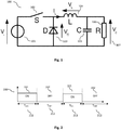
- Fig. 1 illustrates an example buck converter 100.
- Buck converters 100 may be provided in electronic devices e.g. to convert a battery voltage V i 101 into the supply voltage V 0 107 of the load 106.
- a typical buck converter 100 comprises two switches 102, 103 (e. g. a transistor 102 and a diode 103), as well as an inductor 104 and a capacitor 105.
- the two switches 102, 103 control the current through the inductor 104 and thereby provide for a voltage modification (step-down conversion) from the input voltage V i 101 (e.g. a battery voltage) down to the voltage V 0 107 at the load 106.
- V i 101 e.g. a battery voltage
- a buck converter 100 may be operated in a so-called continuous mode, where the current through the inductor 104 never falls to zero.
- the buck converter 100 may be operated in a so-called discontinuous mode for which the current through the inductor may fall to zero during parts of the commutation cycles performed by the two switches 102, 103.
- the buck converter 100 is typically operated in two states forming an overall commutation cycle.
- a first state the switch 102, referred to as the high side switch 102, is closed (on-state), whereas the second switch 103, referred to as the low side switch 103, is open (or whereas the diode 103 is reverse-biased).
- the voltage across the inductor 104 is given by the difference of the input voltage V i 101 and the load voltage V 0 107.
- the energy stored in the inductor 104 increases as the current through the inductor 104 increases.
- a second state (referred to as the off-state of the buck converter 100) the first switch 102 is opened and the second switch 103 is closed (or the diode 103 is forward-biased). If the voltage drop across the second switch 103 (or the diode 103) can be neglected, the voltage across the inductor 104 is the negative voltage V 0 107 across the load 106. During the off-state of the buck converter 100, the energy stored within the inductor 104 is released towards the load 107 via a decreasing current through the inductor 104.
- the buck converter 100 is commutating between the on-state and the off-state in a repetitive manner. This is illustrated in Fig. 2 , where a switching diagram 200 is illustrated. It can be seen that the buck converter 100 commutates between the on-state 201 and the off-state 202 in a periodic manner. By appropriately setting the duration 211 of the on-state and the duration 212 of the off-state, the ratio between the load voltage V 0 107 and the input voltage V i 101 can be tuned. The ratio between the duration 211 of the on-state and the duration of a commutation cycle (i.e. the sum of duration 211 and duration 212) is typically referred to as the duty cycle of the buck converter 100.
- the high side switch 102 is in the on-state and the low side switch 103 is in the off-state.
- the high side switch 102 is in the off-state and the low side switch 103 is in the on-state.
- the performance of the buck converter 100 depends on the characteristics of the different components of the buck converter 100.
- the output capacitor 105 should have enough capacitance to supply sufficient power to the load 106 without any noticeable variations of the load voltage V 0 107 during the different commutation states 201, 202.
- the capacitor 105 should be appropriable selected to reduce output voltage ripples.
- the voltage drop across the diode 103, when forward-biased, or the voltage drop across the transistor 103, when closed should be as low as possible (preferably zero). Due to this reason the low side switch 103 is typically implemented as an N-channel transistor, when implementing the buck converter 100 using a metal oxide-semiconductor (MOS) structure.
- MOS metal oxide-semiconductor
- the low side switch 103 may be implemented as a NMOS transistor.
- N-channel transistors typically have a lower on-resistance R on compared to P-channel transistors.
- R on of an NMOS transistor is in the range of 100m ⁇ whereas the R on of a PMOS transistor is in the range of 1 ⁇ . Consequently, the losses of a buck converter can be reduced by using a NMOS low side transistor 403.
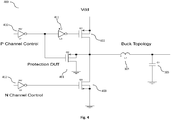
- Fig. 4 illustrates the block diagram of an example buck converter 400 implemented using MOS transistors.
- the high side switch 102 is implemented as a P-channel transistor (i.e. a PMOS transistor) 402.
- the low side switch 103 is implemented as an N-channel transistor 403.
- the buck converter 400 comprises an inductor L1 104 and a capacitor C1 105.
- Fig. 4 shows example control and driver units for the high side transistor 402 and the low side transistor 403.
- These control and driver units may comprise inversion units 410, 411 and 412.
- the inversion units 410, 411 and 412 may also be used as timing elements for controlling the switching instants of the transistors, 401, 402, 403. As such, a delay caused by the inversion units 410, 411, 412 may be adjusted in order to control the switching instants of the transistors, 401, 402, 403.
- NMOS transistor 403 While an NMOS transistor 403 has the advantage of having a low on resistance R on , NMOS transistors are typically disadvantageous in that they have a restricted safe operation area. In other words, N-channel transistors are typically more sensitive than P-channel or PNP transistors.
- the safe operation areas of transistors typically depend on a maximum power which can be taken up by the transistor prior to being destroyed.
- the power absorbed at the NMOS transistor may be defined as the product given by the voltage across the transistor and the current running through the transistor.
- the buck converter 400 should be designed such that the switches 402, 403 (and in particular the NMOS transistor 403) are always operated within their safe operation area, notably when being switched from an off-state to an on-state and/or vice versa.
- the demands on the low side switch 103, 403 of the buck converter 100, 400 are particularly challenging in situations where the low side switch 103, 403 is switched off under load. Such situations may occur when the buck converter 100, 400 has to discharge the capacitor 105, while the low side switch 103, 403 is switched to its off-state.
- the load connected to a buck converter 100, 400 may vary significantly.
- the processors of modem electronic devices are frequently put into a sleep mode and are only activated when required, in view of a more efficient energy management. This may lead to situations, where the load currents requested by the processor vary from a low value (e.g. in the range of 100mA) during sleep mode to a high value (e.g.
- the currents through the low side switch 103, 403 may be significant, if the buck converter is under load (e.g. when the processor connected to the buck converter is activated). The current through the low side switch 103, 403 may be further increased if the load changes (e.g. if the processor is switched off), as this may lead to a discharge of the capacitor 105, thereby providing an additional current through the low side switch 103, 403. In particular, if the load (e.g. the processor) is switched off, the charge in the capacitor 105 has to be discharged via the low side switch 103, 403. This means that the low side switch 103, 403 has to be switched off under current, thereby increasing the risk of operating the low side switch 103, 403 outside the safe operation area.
- the load e.g. the processor
- the current through the low side switch 103, 403 may be significant when switching off the low side switch 103, 403.
- the coil i.e. the inductor 104
- the switch off time of the transistor 103, 403. This leads to an almost instant voltage drop across the low side switch 103, 403 when switching off the low side switch 103, 403, in combination with a high current through the low side switch 103, 403 (due to the relatively slow switch off time of the low side switch 103, 403).
- the low side switch 103, 403 no longer operates in the save operating area, as it is concurrently submitted to a high voltage and a high current. This is illustrated in the diagram 300 of Fig. 3 .
- the current 301 through the low side switch 103, 403 reduces at a slower rate than the increase of the voltage 302 across the low side switch 103, 403. This is due to the relatively slow switch off time (in the range of 1-2ns for low voltage switches, and possibly higher for higher voltage switches) of the low side switch 103, 403 compared to the reaction time of the inductor 104.
- an NMOS based low side switch 403 may leave the save operation area and may be destroyed.
- a possible way of protecting the low side switch 403 could be the use of a snapper capacitor in parallel to the low side switch 403.
- the snapper capacitor absorbs a part of the current through the low side switch 403, thereby reducing the current 301 through the low side switch 403 and thereby protecting the low side switch 403.
- the use of a snapper capacitor is, however, disadvantageous in that the capacitor requires the use of an additional external component (external to the integrated circuit of the buck converter 100, 400).
- the snapper capacitor typically leaks current during normal operation of the buck converter, thereby reducing the efficiency of the buck converter.
- the pass switch 401 (also referred to as the protection switch 401) may be implemented as a more robust P-channel transistor (or as a PNP transistor).
- the protection switch 401 is configured to take over (parts of) the current of the inductor 104, until the low side switch 403 is switched off.
- the voltage drop across the low side switch 403 is limited (e.g. to 2 V) due to the limited R on of the protection switch 401. Consequently, the low side switch 403 can be operated in the save operation area, even when the low side switch 403 is switched off under load.
- the protection switch 401 (which acts as a source follower) may give the coil (i.e. the inductor 104) free.
- the switching times (or the rise times) of the protection switch 401, with respect to the switching times of the low side switch 403 and the high side switch 402, may be appropriately controlled in order to avoid ringing.
- the sequence of the switching times of the low side switch 403, the protection switch 401 and the high side switch 402 is illustrated schematically in the timing diagram 500 in Fig. 5 .
- the low side switch 403 is switched from the on-state to the off-state (timing diagram 501).
- the protection switch 401 is switched from the on-state to the off-state (timing diagram 502).
- the time interval between time instants 511 and 512 can be selected based on the switch off time of the low side switch 403.
- the time interval between time instants 511 and 512 may be set as a fraction of the switch off time of the low side switch 403 (e.g. equal to the switch off time of the low side switch 403).
- the low side switch 403 is not facing concurrently a high voltage 302 (e.g. the output voltage 107) and a high current 301.
- the voltage across the low side switch 403 may be limited to the limited voltage drop across the protection switch 401 (which remains in on-state at the switch-off time instant 511 of the low side switch 403).
- the current 301 through the low side switch 403 may be reduced due to the parallel protection switch 401.
- the switch off time instant 511 of the low side switch 403 and the switch off time instant 512 of the protection switch 401 are illustrated.
- the high side switch 402 may be switched on (at time instant 513 of timing diagram 503).
- the sequence of switching time instants illustrated in Fig. 5 is typically repeated within each commutation cycle of the buck converter 400.
- the protection switch 401 acts as a source follower.
- the low side switch 403 typically an N-channel transistor
- the node i.e. the output voltage at the protection switch 401
- Vt threshold voltage
- the protection switch 401 can take over the current at the low side switch 403 to ground.
- the requirements with regards to the R on of the protection switch 401 can be more relaxed than the R on requirements for the low side switch 403.
- the R on of the protection switch 401 should be selected to ensure that the voltage drop 303 across the protection switch 403 (within the time interval between time instants 511 and 512) is sufficiently small to ensure that the low side switch 403 is operated in the safe operation area (e.g. around 2 Volt to ground).
- the switching off of the protection switch 401 can be synchronized with the high side switch 402, i.e. the switch off time 512 of the protection switch 401 can be synchronized with the switch on time 513 of the high side switch 402, with a short delay of time instant 513 with regards to time instant 512.
- the switch off time 512 of the protection switch 401 can be synchronized with the switch on time 513 of the high side switch 402, with a short delay of time instant 513 with regards to time instant 512.
- the protection switch 401 is active and takes over current, the power dissipation within the protection switch 401 may be quite high. Consequently, there may be a compromise between the delay for switching off the protection switch 401 (i.e. the delay of time instant 512 with regards to time instant 511) and protection.
- the overall time interval between the time instant 511 for switching off the low side switch 402 and the time instant 513 for switching on the high side switch 402 is in a range of ns (1 to 10ns) in a
- a power converter 400 typically comprises a timing generator (analogue or digital) which may be used to control the switches 401, 402, 403 comprised within the power converter 400.
- the inverters (i.e. the timing elements) 410, 411, 412 of Fig. 4 may be adjusted to the specific technology requirements of the power converter 400.
- a power converter 400 may comprise a control unit (comprising e.g. a timing generator and one or more inverters / timing elements) in order to adjust the commutation cycle rate (i.e. the frequency) of the power converter 400 and/or the switching instants 511, 512, 513 of the switches 401, 402, 403 comprised within the power converter 400.
- the switching instants 511, 512, 513 may be adjusted by adjusting a delay caused by the inverters (or timing elements) 410, 411, 412.
- the overall timing of the power converter 400 may be adjusted using an exchangeable and/or programmable storage medium, such as an EPROM (Erasable Programmable Read-Only Memory), an EPROM OTP (One Time Programmable) or an EEPROM (Electrically Erasable Programmable Read-Only Memory).
- an exchangeable and/or programmable storage medium such as an EPROM (Erasable Programmable Read-Only Memory), an EPROM OTP (One Time Programmable) or an EEPROM (Electrically Erasable Programmable Read-Only Memory).
- the power converter 400 may be adapted to a particular application.
- the switching instants (and consequently the losses incurred by the power converter) may be adapted to the particular application (load requirements).
- the use of an exchangeable and/or programmable storage medium would also allow for the adjustment of the switching frequency (i.e. the commutation cycle rate) to the particular application.
- the low side switch 403 may be provided with current sensing means for sensing the current through the low side switch 403.
- the power converter 400 may comprise current sensing means for sensing the current through the low side switch 403.
- the current sensing means may e.g. be implemented as a current mirror.
- the sensed current through the low side switch 403 may be used to adjust the timing "on the fly”.
- the sensed current through the low side switch 403 may be used to adjust the time instants 511, 512, 513.
- the time instant 512 may be determined based on the sensed current through the low side switch 403.
- the losses incurred by the protection switch 401 may be minimized in accordance to the current flowing through the low side switch 403.
- Fig. 6 and 7 illustrate further example power converters 600, 700 comprising alternative example control units for controlling the switching time instants of the transistors 401, 402, 403.
- Fig. 6 illustrates an example power converter 600 for which the control signal of the protection switch 401 is derived from the control signal of the low side switch 403 using an inverter 613 (i.e. derived in dependency of the control signal of the low side switch 403). Furthermore, the inverters 510, 511, 512 are used for controlling the high side switch 402 and the low side switch 403.
- Fig. 7 illustrates an example power converter 700 for which the control signal of the protection switch 401 is generated independently from the control signals of the low side switch 403 and of the high side switch 402.
- the control unit of the power converter 700 comprises the inverters 710, 711, 712, 713.
- the high side switch 402, the low side switch 403 and the protection switch 401 may be implemented as MOS transistors (notably MOS field effect transistors).
- MOS transistors notably MOS field effect transistors.
- a MOS transistor e.g. a PMOS or an NMOS transistor
- MOS transistors 401, 402, 403 are able to block current in only one direction. In the context of a power converter, this means that even though a switch is in the off-state, a current may flow across the body diode of the switch.
- a current may flow across the body diode of the high side switch 402.
- the body diodes 801, 802, 803 of the protection switch 401, the high side switch 402, and the low side switch 403, respectively, are shown in Fig. 8 .
- the low side switch can be maintained in the save operation area during switching.
- the protection switch allows for a fast discharge of the buck capacitor subsequent to a load transient.
- the additional protection switch can be integrated within the integrated circuit of the power converter, thereby making the use of external components (e.g. a snapper capacitor) obsolete.
- the proposed protection switch allows for a protection of the low side switch without additional losses during normal operation of the power converter.
Landscapes
- Engineering & Computer Science (AREA)
- Power Engineering (AREA)
- Dc-Dc Converters (AREA)
Abstract
Description
- The present document relates to power converters. In particular, the present document relates to a scheme for operating a low side switch (notably an N-channel transistor) of a power converter in the safe operation area.
- Switched-mode power supplies are commonly used to convert an input voltage (provided e.g. by a battery of an electronic device) into an output voltage (provided e.g. to a processor of the electronic device). An example for a step-down DC-to-DC converter (providing a lower output voltage from a higher input voltage) is e.g. a so-called buck converter. Such buck converters may comprise N-channel transistors as low side transistors. These N-channel transistors can be destroyed by exceeding the save operation area, when being switched off under load.
- The present document addresses the above mentioned shortcomings of switched-mode power converters. In particular, the present document describes a scheme for protecting the low side switch of a buck converter.
- According to an aspect a power converter, e.g. a DC-to-DC power converter, configured to convert an input voltage at an input of the power converter into an output voltage at an output of the power converter. The power converter may be a switched-mode power converter. In particular, the power converter may be a step-down DC-to-DC converter such as a buck converter. Alternatively, the power converter may be a step-up DC-to-DC converter such as a boost converter. The power converter may comprise a high side switch connectable in series to an inductor (which may be external to an integrated circuit comprising the power converter). The inductor may have the function of storing energy to be provided to a load at the output of the power converter. The high side switch may be configured to couple the inductor (if connected to the high side switch) to the input voltage or to the output voltage during an on-state of the high side switch. If the power converter is a step-down converter (e.g. a buck converter), the high side switch may be configured to couple the inductor to the input voltage. If the power converter is a step-up converter (e.g. a boost converter), the high side switch may be configured to couple the inductor to the output voltage.
- It should be noted that the high side switch may comprise or may be implemented as a diode. In particular, the high side switch may comprise a body diode (as is the case e.g. for a MOS transistor). Alternatively, the high side switch may be implemented as a diode (e.g. if the power converter is a step-up converter such as a boost converter). In general terms, it may be stated that the power converter may comprise a high side switch or a diode connectable in series to the inductor, wherein the high side switch or the diode may be configured to couple the inductor to the input voltage or to the output voltage, during an on-state of the high side switch, or when the diode is forward biased.
- In the present document, the term "couple" or "coupled" refers to elements being in electrical communication with each other, whether directly connected e.g., via wires, or in some other manner.
- The power converter may be a multi-phase power converter. This may be beneficial to provide a power converter for increased load requirements. Such a multi-phase power converter may comprise a plurality of power converters (comprising e.g. a high side switch and a low side switch, each) in parallel. The plurality of power converters may share a common commutation cycle rate, wherein the switching instants of the respective (high side) switches may be offset with respect to one another.
- The power converter comprises a low side switch configured to couple the inductor to ground during an on-state of the low side switch. Typically, the low side switch and the high side switch are controlled such that when the high side switch is in the on-state, the low side switch is in the off-state, and vice versa.
- In addition, the power converter comprises a protection switch in parallel to the low side switch, and configured to reduce a voltage drop across the low side switch during at least part of a switch off time of the low side switch. The switch off time of the low side switch may be the time interval required by the low side switch to reduce the current through the low side switch from 100% (when the low side switch is in the on-state) to a pre-determined off threshold (of e.g. 10%, 20%, 30%, 40% or 50%).
- The low side switch may be an N-channel transistor (i.e. an NMOS transistor). The protection switch may be a P-channel transistor (i.e. a PMOS transistor) or a PNP transistor. The high side switch may be a P-channel transistor.
- The power converter may further comprise a control unit configured to control switching times of the high side switch, the low side switch and/or the protection switch. The control unit may be configured to switch off the low side switch at a first time instant, and switch off the protection switch at a subsequent second time instant. The time interval between the first and second time instants may correspond to at least part of the switch off time of the low side switch. In particular, the time interval between the first and second time instants may be 50% or more, 60% or more, 70% or more, 80% or more, 90% or more, 100% or more of the switch off time of the low side switch.
- The control unit may be configured to switch on the high side switch at a third time instant subsequent to the second time instant. Furthermore, the control unit may be configured to switch on the protection switch subsequent to switching off the high side switch and not later than switching on the low side switch. The latter case may be beneficial in situations where the low side switch is submitted to an overload. In such cases, the protection switch may support the low side switch to drive the required current. This can be particularly helpful for a step-up converter (such as a boost converter).
- Typically, the control unit is configured to repeatedly switch between the on- and off-states of the high side switch, the low side switch and/or the protection switch in accordance to a commutation cycle rate of the power converter. The commutation cycle rate may be the time interval between the (beginning of) two subsequent periodic on-states of the high side switch.
- The control unit may be configured to control the high side switch, the low side switch and/or the protection switch such that when the high side switch is in the on-state, the protection switch and the low side switch are in the off-state; and/or when the low side switch is in the on-state, the high side switch is in the off-state.
- The power converter may further comprise current sensing means configured to sense a current through the low side switch. The current sensing means may be implemented using a current mirror. The part of the switch off time of the low side switch during which the protection switch reduces the voltage drop across the low side switch may be determined based on the sensed current. In particular, the control unit may be configured to determine the time interval between the first and second time instants based on the sensed current. In other words, the control unit may be configured to determine the switch-off time of the protection switch based on the sensed current. The time interval between the first and second time instants may be reduced if the sensed current reduces (and vice versa). As such, the low side switch may be operated in the safe operation area, while reducing the losses caused by the protection switch.
- It should be noted that the methods and systems including its preferred embodiments as outlined in the present document may be used stand-alone or in combination with the other systems disclosed in this document. Furthermore, all aspects of the systems outlined in the present document may be arbitrarily combined. In particular, the features of the claims may be combined with one another in an arbitrary manner.
- The invention is explained below in an exemplary manner with reference to the accompanying drawings, wherein
-
Fig. 1 illustrates a block diagram of an example buck converter; -
Fig. 2 illustrates a switching diagram for an example buck converter; -
Fig. 3 shows example currents and voltages at the low side switch of an example buck converter; -
Fig. 4 illustrates an example buck converter comprising a protection switch; -
Fig. 5 illustrates an example timing diagram for switching the low side switch of a buck converter from on-state to off-state; -
Figs. 6 and7 illustrate further example buck converters with example control circuits; and -
Fig. 8 illustrates the example buck converter ofFigs. 4 comprising MOS transistors with body diodes. -
Fig. 1 illustrates anexample buck converter 100.Buck converters 100 may be provided in electronic devices e.g. to convert abattery voltage V i 101 into thesupply voltage V 0 107 of theload 106. Atypical buck converter 100 comprises twoswitches 102, 103 (e. g. atransistor 102 and a diode 103), as well as aninductor 104 and acapacitor 105. The twoswitches inductor 104 and thereby provide for a voltage modification (step-down conversion) from the input voltage Vi 101 (e.g. a battery voltage) down to thevoltage V 0 107 at theload 106. Abuck converter 100 may be operated in a so-called continuous mode, where the current through theinductor 104 never falls to zero. Alternatively, thebuck converter 100 may be operated in a so-called discontinuous mode for which the current through the inductor may fall to zero during parts of the commutation cycles performed by the twoswitches - The
buck converter 100 is typically operated in two states forming an overall commutation cycle. In a first state theswitch 102, referred to as thehigh side switch 102, is closed (on-state), whereas thesecond switch 103, referred to as thelow side switch 103, is open (or whereas thediode 103 is reverse-biased). During this first state (referred to as the on-state of the buck converter 100) the voltage across theinductor 104 is given by the difference of theinput voltage V i 101 and theload voltage V 0 107. During this first stage the energy stored in theinductor 104 increases as the current through theinductor 104 increases. In a second state (referred to as the off-state of the buck converter 100) thefirst switch 102 is opened and thesecond switch 103 is closed (or thediode 103 is forward-biased). If the voltage drop across the second switch 103 (or the diode 103) can be neglected, the voltage across theinductor 104 is thenegative voltage V 0 107 across theload 106. During the off-state of thebuck converter 100, the energy stored within theinductor 104 is released towards theload 107 via a decreasing current through theinductor 104. - In order to provide a voltage conversion of the
input voltage V i 101 to theload voltage V 0 107, thebuck converter 100 is commutating between the on-state and the off-state in a repetitive manner. This is illustrated inFig. 2 , where a switching diagram 200 is illustrated. It can be seen that thebuck converter 100 commutates between the on-state 201 and the off-state 202 in a periodic manner. By appropriately setting theduration 211 of the on-state and theduration 212 of the off-state, the ratio between theload voltage V 0 107 and theinput voltage V i 101 can be tuned. The ratio between theduration 211 of the on-state and the duration of a commutation cycle (i.e. the sum ofduration 211 and duration 212) is typically referred to as the duty cycle of thebuck converter 100. - During the on-state of the
buck converter 100, thehigh side switch 102 is in the on-state and thelow side switch 103 is in the off-state. During the off-state of thebuck converter 100, thehigh side switch 102 is in the off-state and thelow side switch 103 is in the on-state. - The performance of the
buck converter 100 depends on the characteristics of the different components of thebuck converter 100. As such, theoutput capacitor 105 should have enough capacitance to supply sufficient power to theload 106 without any noticeable variations of theload voltage V 0 107 during the different commutation states 201, 202. In other words, thecapacitor 105 should be appropriable selected to reduce output voltage ripples. Furthermore, the voltage drop across thediode 103, when forward-biased, or the voltage drop across thetransistor 103, when closed, should be as low as possible (preferably zero). Due to this reason thelow side switch 103 is typically implemented as an N-channel transistor, when implementing thebuck converter 100 using a metal oxide-semiconductor (MOS) structure. In other words, thelow side switch 103 may be implemented as a NMOS transistor. This is advantageous due to the fact that N-channel transistors typically have a lower on-resistance Ron compared to P-channel transistors. A typical value for the Ron of an NMOS transistor is in the range of 100mΩ whereas the Ron of a PMOS transistor is in the range of 1Ω. Consequently, the losses of a buck converter can be reduced by using a NMOSlow side transistor 403. -
Fig. 4 illustrates the block diagram of anexample buck converter 400 implemented using MOS transistors. Thehigh side switch 102 is implemented as a P-channel transistor (i.e. a PMOS transistor) 402. Thelow side switch 103 is implemented as an N-channel transistor 403. Furthermore, thebuck converter 400 comprises aninductor L1 104 and acapacitor C1 105. In addition,Fig. 4 shows example control and driver units for thehigh side transistor 402 and thelow side transistor 403. These control and driver units may compriseinversion units inversion units inversion units - While an
NMOS transistor 403 has the advantage of having a low on resistance Ron, NMOS transistors are typically disadvantageous in that they have a restricted safe operation area. In other words, N-channel transistors are typically more sensitive than P-channel or PNP transistors. The safe operation areas of transistors typically depend on a maximum power which can be taken up by the transistor prior to being destroyed. The power absorbed at the NMOS transistor may be defined as the product given by the voltage across the transistor and the current running through the transistor. Thebuck converter 400 should be designed such that theswitches 402, 403 (and in particular the NMOS transistor 403) are always operated within their safe operation area, notably when being switched from an off-state to an on-state and/or vice versa. - The demands on the
low side switch buck converter low side switch buck converter capacitor 105, while thelow side switch buck converter low side switch low side switch capacitor 105, thereby providing an additional current through thelow side switch capacitor 105 has to be discharged via thelow side switch low side switch low side switch - Consequently, the current through the
low side switch low side switch transistor low side switch low side switch low side switch 103, 403 (due to the relatively slow switch off time of thelow side switch 103, 403). Hence, there is a risk that thelow side switch Fig. 3 . It can be seen that the current 301 through thelow side switch voltage 302 across thelow side switch low side switch inductor 104. - As a result of the concurrent
high voltage 302 and high current 301, an NMOS basedlow side switch 403 may leave the save operation area and may be destroyed. A possible way of protecting thelow side switch 403 could be the use of a snapper capacitor in parallel to thelow side switch 403. When switching off thelow side switch 403, the snapper capacitor absorbs a part of the current through thelow side switch 403, thereby reducing the current 301 through thelow side switch 403 and thereby protecting thelow side switch 403. The use of a snapper capacitor is, however, disadvantageous in that the capacitor requires the use of an additional external component (external to the integrated circuit of thebuck converter 100, 400). Furthermore, the snapper capacitor typically leaks current during normal operation of the buck converter, thereby reducing the efficiency of the buck converter. - In the present document it is proposed to use a
pass switch 401 in parallel to thelow side switch 403 in order to ensure that thelow side switch 403 stays within the save operating area. The pass switch 401 (also referred to as the protection switch 401) may be implemented as a more robust P-channel transistor (or as a PNP transistor). Theprotection switch 401 is configured to take over (parts of) the current of theinductor 104, until thelow side switch 403 is switched off. - At the same time, the voltage drop across the
low side switch 403 is limited (e.g. to 2 V) due to the limited Ron of theprotection switch 401. Consequently, thelow side switch 403 can be operated in the save operation area, even when thelow side switch 403 is switched off under load. Once thelow side switch 403 is completely switched off (i.e. subsequent to the expiration of the switch off time), the protection switch 401 (which acts as a source follower) may give the coil (i.e. the inductor 104) free. The switching times (or the rise times) of theprotection switch 401, with respect to the switching times of thelow side switch 403 and thehigh side switch 402, may be appropriately controlled in order to avoid ringing. - The sequence of the switching times of the
low side switch 403, theprotection switch 401 and thehigh side switch 402 is illustrated schematically in the timing diagram 500 inFig. 5 . Attime instant 511, thelow side switch 403 is switched from the on-state to the off-state (timing diagram 501). Subsequently, attime instant 512, theprotection switch 401 is switched from the on-state to the off-state (timing diagram 502). The time interval betweentime instants low side switch 403. By way of example, the time interval betweentime instants - As such, it can be ensured that during switch off, the
low side switch 403 is not facing concurrently a high voltage 302 (e.g. the output voltage 107) and a high current 301. In particular, the voltage across thelow side switch 403 may be limited to the limited voltage drop across the protection switch 401 (which remains in on-state at the switch-off time instant 511 of the low side switch 403). Furthermore, the current 301 through thelow side switch 403 may be reduced due to theparallel protection switch 401. Hence, it can be ensured that thelow side switch 403 stays within the safe operation area. This is illustrated inFig. 3 , where the switch offtime instant 511 of thelow side switch 403 and the switch offtime instant 512 of theprotection switch 401 are illustrated. It can be seen that in the time interval betweentime instants low side switch 403, thevoltage 303 across thelow side switch 403 can be reduced, compared to a situation (voltage 302) withoutprotection switch 401. - Returning to
Fig. 5 , it can be seen that subsequent to switching off theprotection switch 401 attime instant 512, thehigh side switch 402 may be switched on (attime instant 513 of timing diagram 503). The sequence of switching time instants illustrated inFig. 5 is typically repeated within each commutation cycle of thebuck converter 400. - Overall, the protection switch 401 (e.g. a P-channel transistor) acts as a source follower. When the low side switch 403 (typically an N-channel transistor) switches off under load (at time instant 511), the node (i.e. the output voltage at the protection switch 401) will ramp to the threshold voltage Vt of the
protection switch 401. This may automatically lead to theprotection switch 401 being in the on-state (without the need to explicitly switch theprotection switch 401 into the on-state). Hence, theprotection switch 401 can take over the current at thelow side switch 403 to ground. The requirements with regards to the Ron of theprotection switch 401 can be more relaxed than the Ron requirements for thelow side switch 403. The Ron of theprotection switch 401 should be selected to ensure that thevoltage drop 303 across the protection switch 403 (within the time interval betweentime instants 511 and 512) is sufficiently small to ensure that thelow side switch 403 is operated in the safe operation area (e.g. around 2 Volt to ground). - The switching off of the
protection switch 401 can be synchronized with thehigh side switch 402, i.e. the switch offtime 512 of theprotection switch 401 can be synchronized with the switch ontime 513 of thehigh side switch 402, with a short delay oftime instant 513 with regards totime instant 512. By controlling therise time 512 of the gate of theprotection switch 401, ringing can be avoided. If theprotection switch 401 is active and takes over current, the power dissipation within theprotection switch 401 may be quite high. Consequently, there may be a compromise between the delay for switching off the protection switch 401 (i.e. the delay oftime instant 512 with regards to time instant 511) and protection. In general, the overall time interval between thetime instant 511 for switching off thelow side switch 402 and thetime instant 513 for switching on thehigh side switch 402 is in a range of ns (1 to 10ns) in a low voltage application. - A
power converter 400 typically comprises a timing generator (analogue or digital) which may be used to control theswitches power converter 400. The inverters (i.e. the timing elements) 410, 411, 412 ofFig. 4 may be adjusted to the specific technology requirements of thepower converter 400. As such, apower converter 400 may comprise a control unit (comprising e.g. a timing generator and one or more inverters / timing elements) in order to adjust the commutation cycle rate (i.e. the frequency) of thepower converter 400 and/or the switchinginstants switches power converter 400. The switchinginstants - The overall timing of the
power converter 400 may be adjusted using an exchangeable and/or programmable storage medium, such as an EPROM (Erasable Programmable Read-Only Memory), an EPROM OTP (One Time Programmable) or an EEPROM (Electrically Erasable Programmable Read-Only Memory). As such, thepower converter 400 may be adapted to a particular application. In particular, the switching instants (and consequently the losses incurred by the power converter) may be adapted to the particular application (load requirements). The use of an exchangeable and/or programmable storage medium would also allow for the adjustment of the switching frequency (i.e. the commutation cycle rate) to the particular application. - The
low side switch 403 may be provided with current sensing means for sensing the current through thelow side switch 403. In other words, thepower converter 400 may comprise current sensing means for sensing the current through thelow side switch 403. The current sensing means may e.g. be implemented as a current mirror. The sensed current through thelow side switch 403 may be used to adjust the timing "on the fly". In other words, the sensed current through thelow side switch 403 may be used to adjust thetime instants time instant 512 may be determined based on the sensed current through thelow side switch 403. Hence, the losses incurred by theprotection switch 401 may be minimized in accordance to the current flowing through thelow side switch 403. -
Fig. 6 and7 illustrate furtherexample power converters transistors Fig. 6 illustrates anexample power converter 600 for which the control signal of theprotection switch 401 is derived from the control signal of thelow side switch 403 using an inverter 613 (i.e. derived in dependency of the control signal of the low side switch 403). Furthermore, theinverters high side switch 402 and thelow side switch 403.Fig. 7 illustrates anexample power converter 700 for which the control signal of theprotection switch 401 is generated independently from the control signals of thelow side switch 403 and of thehigh side switch 402. For this purpose, the control unit of thepower converter 700 comprises theinverters - As indicated above, the
high side switch 402, thelow side switch 403 and theprotection switch 401 may be implemented as MOS transistors (notably MOS field effect transistors). A MOS transistor (e.g. a PMOS or an NMOS transistor) typically comprises a body diode between the drain (cathode) and the source (anode) of the MOS transistor. As a consequence of such body diodes, theMOS transistors high side switch 402 and subsequent to switching off the protection switch 401 (i.e. betweentime instants 512 and 513), a current may flow across the body diode of thehigh side switch 402. Thebody diodes protection switch 401, thehigh side switch 402, and thelow side switch 403, respectively, are shown inFig. 8 . - In the present document a system for protecting the low side switch of a switched mode power converter have been described. By using a protection switch in parallel to the low side switch, the low side switch can be maintained in the save operation area during switching. Furthermore, the protection switch allows for a fast discharge of the buck capacitor subsequent to a load transient. The additional protection switch can be integrated within the integrated circuit of the power converter, thereby making the use of external components (e.g. a snapper capacitor) obsolete. Furthermore, the proposed protection switch allows for a protection of the low side switch without additional losses during normal operation of the power converter.
- It should be noted that the description and drawings merely illustrate the principles of the proposed methods and systems. Those skilled in the art will be able to implement various arrangements that, although not explicitly described or shown herein, embody the principles of the invention and are included within its spirit and scope. Furthermore, all examples and embodiment outlined in the present document are principally intended expressly to be only for explanatory purposes to help the reader in understanding the principles of the proposed methods and systems. Furthermore, all statements herein providing principles, aspects, and embodiments of the invention, as well as specific examples thereof, are intended to encompass equivalents thereof.
Claims (14)
- A power converter (400) configured to convert an input voltage (101) at an input of the power converter (400) into an output voltage (107) at an output of the power converter (400), wherein the power converter (400) comprises- a low side switch (403) configured to couple an inductor (104) to ground during an on-state of the low side switch (403); wherein the inductor (104) is configured to store energy to be provided to a load at the output of the power converter (400); and- a protection switch (401) in parallel to the low side switch (403), configured to reduce a voltage drop across the low side switch (403) during at least part of a switch off time of the low side switch (403).
- The power converter (400) of claim 1, wherein the low side switch (403) is an N-channel transistor.
- The power converter (400) of any previous claim, further comprising a high side switch (402) connectable in series to the inductor (104), configured to couple the inductor (104) to the input voltage (101) or to the output voltage (107) during an on-state of the high side switch (402).
- The power converter (400) of claim 3, wherein- the power converter (400) is a buck converter; and- the high side switch (402) is configured to couple the inductor (104) to the input voltage (101).
- The power converter (400) of claim 3, wherein- the power converter (400) is a boost converter; and- the high side switch (402) is configured to couple the inductor (104) to the output voltage (107).
- The power converter (400) of any of claims 3 to 5, further comprising a control unit (410, 411, 412) configured to control switching times (511, 512, 513) of the high side switch (402), the low side switch (403) and the protection switch (401).
- The power converter (400) of claim 6, wherein the control unit (410, 411, 412) is configured to- switch off the low side switch (403) at a first time instant (511);- switch off the protection switch (401) at a subsequent second time instant (512).
- The power converter (400) of claim 7, wherein the time interval between the first (511) and second (512) time instants is greater or equal to the switch off time of the low side switch (403).
- The power converter (400) of any of claims 7 to 8, wherein the control unit (410, 411, 412) is configured to switch on the high side switch (402) at a third time instant (513) subsequent to the second time instant (512).
- The power converter (400) of any of claims 7 to 9, wherein the control unit (410, 411, 412) is configured to switch on the protection switch (401) subsequent to switching off the high side switch (402) and not later than switching on the low side switch (403).
- The power converter (400) of any of claims 6 to 10, wherein the control unit (410, 411, 412) is configured to repeatedly switch between the on- and off-states of the high side switch (402), the low side switch (403) and the protection switch (401) in accordance to a commutation cycle rate of the power converter (400).
- The power converter (400) of claim 11, wherein the control unit (410, 411, 412) is configured to control the high side switch (402), the low side switch (403) and the protection switch (401) such that- when the high side switch (402) is in the on-state, the protection switch (401) and the low side switch (403) is in the off-state; and- when the low side switch (403) is in the on-state, the high side switch (402) is in the off-state.
- The power converter (400) of any previous claim, wherein the protection switch (403) is a P-channel transistor or a PNP transistor.
- The power converter (400) of any previous claims, further comprising- current sensing means configured to sense a current through the low side switch (403); wherein the part of the switch off time of the low side switch (403) during which the protection switch (401) reduces the voltage drop across the low side switch (403) is determined based on the sensed current.
Priority Applications (2)
| Application Number | Priority Date | Filing Date | Title |
|---|---|---|---|
| EP12153920.9A EP2624426A1 (en) | 2012-02-03 | 2012-02-03 | Protection of an N-channel transistor |
| US13/478,768 US20130200868A1 (en) | 2012-02-03 | 2012-05-23 | Protection of an N-Channel Transistor |
Applications Claiming Priority (1)
| Application Number | Priority Date | Filing Date | Title |
|---|---|---|---|
| EP12153920.9A EP2624426A1 (en) | 2012-02-03 | 2012-02-03 | Protection of an N-channel transistor |
Publications (1)
| Publication Number | Publication Date |
|---|---|
| EP2624426A1 true EP2624426A1 (en) | 2013-08-07 |
Family
ID=45554576
Family Applications (1)
| Application Number | Title | Priority Date | Filing Date |
|---|---|---|---|
| EP12153920.9A Withdrawn EP2624426A1 (en) | 2012-02-03 | 2012-02-03 | Protection of an N-channel transistor |
Country Status (2)
| Country | Link |
|---|---|
| US (1) | US20130200868A1 (en) |
| EP (1) | EP2624426A1 (en) |
Cited By (1)
| Publication number | Priority date | Publication date | Assignee | Title |
|---|---|---|---|---|
| WO2016165326A1 (en) * | 2015-04-17 | 2016-10-20 | 华为技术有限公司 | Voltage conversion circuit |
Families Citing this family (4)
| Publication number | Priority date | Publication date | Assignee | Title |
|---|---|---|---|---|
| TW201340078A (en) * | 2012-03-22 | 2013-10-01 | Richtek Technology Corp | Voltage conversion circuit and method for improving efficiency of a driver |
| CN103715870B (en) * | 2013-12-26 | 2016-06-29 | 华为技术有限公司 | Voltage adjuster and resonant gate driver thereof |
| CN107800295A (en) * | 2016-09-07 | 2018-03-13 | 国民技术股份有限公司 | A kind of type of voltage step-up/down converter and its method of work and terminal device |
| US11942863B2 (en) * | 2018-11-05 | 2024-03-26 | Rohm Co., Ltd. | Switching power supply including a logic circuit to control a discharge circuit |
Citations (2)
| Publication number | Priority date | Publication date | Assignee | Title |
|---|---|---|---|---|
| US20100013451A1 (en) | 2008-07-16 | 2010-01-21 | Kabushiki Kaisha Toshiba | Semiconductor device |
| US20100109625A1 (en) | 2007-11-29 | 2010-05-06 | Rohm Co., Ltd. | Switching regulator and control circuit thereof |
-
2012
- 2012-02-03 EP EP12153920.9A patent/EP2624426A1/en not_active Withdrawn
- 2012-05-23 US US13/478,768 patent/US20130200868A1/en not_active Abandoned
Patent Citations (2)
| Publication number | Priority date | Publication date | Assignee | Title |
|---|---|---|---|---|
| US20100109625A1 (en) | 2007-11-29 | 2010-05-06 | Rohm Co., Ltd. | Switching regulator and control circuit thereof |
| US20100013451A1 (en) | 2008-07-16 | 2010-01-21 | Kabushiki Kaisha Toshiba | Semiconductor device |
Cited By (3)
| Publication number | Priority date | Publication date | Assignee | Title |
|---|---|---|---|---|
| WO2016165326A1 (en) * | 2015-04-17 | 2016-10-20 | 华为技术有限公司 | Voltage conversion circuit |
| US10148182B2 (en) | 2015-04-17 | 2018-12-04 | Huawei Technologies Co., Ltd. | Voltage conversion circuit with bleed module |
| US10680519B2 (en) | 2015-04-17 | 2020-06-09 | Huawei Technologies Co., Ltd. | Voltage conversion circuit with a bleed circuit |
Also Published As
| Publication number | Publication date |
|---|---|
| US20130200868A1 (en) | 2013-08-08 |
Similar Documents
| Publication | Publication Date | Title |
|---|---|---|
| US10090663B2 (en) | Over-current protection circuit and method for voltage regulators | |
| CN105391298B (en) | Dc-dc converter control | |
| JP6402591B2 (en) | Semiconductor device | |
| US11539294B2 (en) | Multi-level power converter with light load flying capacitor voltage regulation | |
| JP6382002B2 (en) | DC-DC converter | |
| US8450988B2 (en) | Systems and methods for controlling inductive energy in DC-DC converters | |
| US9417642B2 (en) | Bootstrap DC-DC converter | |
| US9729061B2 (en) | Boost regulator having adaptive dead time | |
| US20170353105A1 (en) | Method and circuitry to soft start high power charge pumps | |
| US9531264B2 (en) | Auxiliary recharge | |
| US10243451B1 (en) | System and method for powering a switching converter | |
| US8637909B1 (en) | Mixed mode dual switch | |
| US8907641B2 (en) | Circuit and method for short circuit protection | |
| US8497719B2 (en) | Slew rate PWM controlled charge pump for limited in-rush current switch driving | |
| US20130200868A1 (en) | Protection of an N-Channel Transistor | |
| JPWO2020095748A1 (en) | Switching power supply | |
| US7911192B2 (en) | High voltage power regulation using two power switches with low voltage transistors | |
| US20060192589A1 (en) | Inverter apparatus with improved gate drive for power MOSFET | |
| US10523118B2 (en) | Reverse recovery charge elimination in DC/DC power converters | |
| US20110121805A1 (en) | Active Power Switch Topology for Switching Regulators | |
| US8569811B1 (en) | Self clamping FET devices in circuits using transient sources | |
| US9866104B2 (en) | Circuits and methods for operating a switching regulator | |
| EP1800389A2 (en) | Voltage converter for converting a voltage to multiple output voltages and method of operating said voltage converter | |
| US12051963B2 (en) | Minimum peak current for power converter | |
| US8872576B2 (en) | Recharging of the gate charge of a transistor |
Legal Events
| Date | Code | Title | Description |
|---|---|---|---|
| PUAI | Public reference made under article 153(3) epc to a published international application that has entered the european phase |
Free format text: ORIGINAL CODE: 0009012 |
|
| AK | Designated contracting states |
Kind code of ref document: A1 Designated state(s): AL AT BE BG CH CY CZ DE DK EE ES FI FR GB GR HR HU IE IS IT LI LT LU LV MC MK MT NL NO PL PT RO RS SE SI SK SM TR |
|
| AX | Request for extension of the european patent |
Extension state: BA ME |
|
| 17P | Request for examination filed |
Effective date: 20131210 |
|
| RBV | Designated contracting states (corrected) |
Designated state(s): AL AT BE BG CH CY CZ DE DK EE ES FI FR GB GR HR HU IE IS IT LI LT LU LV MC MK MT NL NO PL PT RO RS SE SI SK SM TR |
|
| STAA | Information on the status of an ep patent application or granted ep patent |
Free format text: STATUS: EXAMINATION IS IN PROGRESS |
|
| 17Q | First examination report despatched |
Effective date: 20170228 |
|
| STAA | Information on the status of an ep patent application or granted ep patent |
Free format text: STATUS: THE APPLICATION HAS BEEN WITHDRAWN |
|
| 18W | Application withdrawn |
Effective date: 20170427 |