EP2624283A1 - Sapphire substrate and semiconductor light-emitting element - Google Patents
Sapphire substrate and semiconductor light-emitting element Download PDFInfo
- Publication number
- EP2624283A1 EP2624283A1 EP11814741.2A EP11814741A EP2624283A1 EP 2624283 A1 EP2624283 A1 EP 2624283A1 EP 11814741 A EP11814741 A EP 11814741A EP 2624283 A1 EP2624283 A1 EP 2624283A1
- Authority
- EP
- European Patent Office
- Prior art keywords
- projections
- sapphire substrate
- center
- nitride semiconductor
- substrate according
- Prior art date
- Legal status (The legal status is an assumption and is not a legal conclusion. Google has not performed a legal analysis and makes no representation as to the accuracy of the status listed.)
- Granted
Links
Images




Classifications
-
- H—ELECTRICITY
- H10—SEMICONDUCTOR DEVICES; ELECTRIC SOLID-STATE DEVICES NOT OTHERWISE PROVIDED FOR
- H10H—INORGANIC LIGHT-EMITTING SEMICONDUCTOR DEVICES HAVING POTENTIAL BARRIERS
- H10H20/00—Individual inorganic light-emitting semiconductor devices having potential barriers, e.g. light-emitting diodes [LED]
- H10H20/80—Constructional details
- H10H20/81—Bodies
- H10H20/819—Bodies characterised by their shape, e.g. curved or truncated substrates
- H10H20/82—Roughened surfaces, e.g. at the interface between epitaxial layers
-
- H—ELECTRICITY
- H10—SEMICONDUCTOR DEVICES; ELECTRIC SOLID-STATE DEVICES NOT OTHERWISE PROVIDED FOR
- H10H—INORGANIC LIGHT-EMITTING SEMICONDUCTOR DEVICES HAVING POTENTIAL BARRIERS
- H10H20/00—Individual inorganic light-emitting semiconductor devices having potential barriers, e.g. light-emitting diodes [LED]
- H10H20/01—Manufacture or treatment
- H10H20/011—Manufacture or treatment of bodies, e.g. forming semiconductor layers
- H10H20/013—Manufacture or treatment of bodies, e.g. forming semiconductor layers having light-emitting regions comprising only Group III-V materials
- H10H20/0133—Manufacture or treatment of bodies, e.g. forming semiconductor layers having light-emitting regions comprising only Group III-V materials with a substrate not being Group III-V materials
- H10H20/01335—Manufacture or treatment of bodies, e.g. forming semiconductor layers having light-emitting regions comprising only Group III-V materials with a substrate not being Group III-V materials the light-emitting regions comprising nitride materials
-
- H—ELECTRICITY
- H10—SEMICONDUCTOR DEVICES; ELECTRIC SOLID-STATE DEVICES NOT OTHERWISE PROVIDED FOR
- H10H—INORGANIC LIGHT-EMITTING SEMICONDUCTOR DEVICES HAVING POTENTIAL BARRIERS
- H10H20/00—Individual inorganic light-emitting semiconductor devices having potential barriers, e.g. light-emitting diodes [LED]
- H10H20/80—Constructional details
- H10H20/81—Bodies
- H10H20/814—Bodies having reflecting means, e.g. semiconductor Bragg reflectors
-
- H—ELECTRICITY
- H10—SEMICONDUCTOR DEVICES; ELECTRIC SOLID-STATE DEVICES NOT OTHERWISE PROVIDED FOR
- H10H—INORGANIC LIGHT-EMITTING SEMICONDUCTOR DEVICES HAVING POTENTIAL BARRIERS
- H10H20/00—Individual inorganic light-emitting semiconductor devices having potential barriers, e.g. light-emitting diodes [LED]
- H10H20/80—Constructional details
- H10H20/81—Bodies
- H10H20/819—Bodies characterised by their shape, e.g. curved or truncated substrates
-
- H—ELECTRICITY
- H10—SEMICONDUCTOR DEVICES; ELECTRIC SOLID-STATE DEVICES NOT OTHERWISE PROVIDED FOR
- H10H—INORGANIC LIGHT-EMITTING SEMICONDUCTOR DEVICES HAVING POTENTIAL BARRIERS
- H10H20/00—Individual inorganic light-emitting semiconductor devices having potential barriers, e.g. light-emitting diodes [LED]
- H10H20/80—Constructional details
- H10H20/81—Bodies
- H10H20/822—Materials of the light-emitting regions
- H10H20/824—Materials of the light-emitting regions comprising only Group III-V materials, e.g. GaP
- H10H20/825—Materials of the light-emitting regions comprising only Group III-V materials, e.g. GaP containing nitrogen, e.g. GaN
-
- H—ELECTRICITY
- H10—SEMICONDUCTOR DEVICES; ELECTRIC SOLID-STATE DEVICES NOT OTHERWISE PROVIDED FOR
- H10P—GENERIC PROCESSES OR APPARATUS FOR THE MANUFACTURE OR TREATMENT OF DEVICES COVERED BY CLASS H10
- H10P14/00—Formation of materials, e.g. in the shape of layers or pillars
- H10P14/20—Formation of materials, e.g. in the shape of layers or pillars of semiconductor materials
- H10P14/29—Formation of materials, e.g. in the shape of layers or pillars of semiconductor materials characterised by the substrates
- H10P14/2901—Materials
- H10P14/2921—Materials being crystalline insulating materials
-
- H—ELECTRICITY
- H10—SEMICONDUCTOR DEVICES; ELECTRIC SOLID-STATE DEVICES NOT OTHERWISE PROVIDED FOR
- H10P—GENERIC PROCESSES OR APPARATUS FOR THE MANUFACTURE OR TREATMENT OF DEVICES COVERED BY CLASS H10
- H10P14/00—Formation of materials, e.g. in the shape of layers or pillars
- H10P14/20—Formation of materials, e.g. in the shape of layers or pillars of semiconductor materials
- H10P14/29—Formation of materials, e.g. in the shape of layers or pillars of semiconductor materials characterised by the substrates
- H10P14/2924—Structures
- H10P14/2925—Surface structures
-
- H—ELECTRICITY
- H10—SEMICONDUCTOR DEVICES; ELECTRIC SOLID-STATE DEVICES NOT OTHERWISE PROVIDED FOR
- H10P—GENERIC PROCESSES OR APPARATUS FOR THE MANUFACTURE OR TREATMENT OF DEVICES COVERED BY CLASS H10
- H10P14/00—Formation of materials, e.g. in the shape of layers or pillars
- H10P14/20—Formation of materials, e.g. in the shape of layers or pillars of semiconductor materials
- H10P14/32—Formation of materials, e.g. in the shape of layers or pillars of semiconductor materials characterised by intermediate layers between substrates and deposited layers
- H10P14/3202—Materials thereof
- H10P14/3214—Materials thereof being Group IIIA-VA semiconductors
- H10P14/3216—Nitrides
-
- H—ELECTRICITY
- H10—SEMICONDUCTOR DEVICES; ELECTRIC SOLID-STATE DEVICES NOT OTHERWISE PROVIDED FOR
- H10P—GENERIC PROCESSES OR APPARATUS FOR THE MANUFACTURE OR TREATMENT OF DEVICES COVERED BY CLASS H10
- H10P14/00—Formation of materials, e.g. in the shape of layers or pillars
- H10P14/20—Formation of materials, e.g. in the shape of layers or pillars of semiconductor materials
- H10P14/34—Deposited materials, e.g. layers
- H10P14/3402—Deposited materials, e.g. layers characterised by the chemical composition
- H10P14/3414—Deposited materials, e.g. layers characterised by the chemical composition being group IIIA-VIA materials
- H10P14/3416—Nitrides
-
- Y—GENERAL TAGGING OF NEW TECHNOLOGICAL DEVELOPMENTS; GENERAL TAGGING OF CROSS-SECTIONAL TECHNOLOGIES SPANNING OVER SEVERAL SECTIONS OF THE IPC; TECHNICAL SUBJECTS COVERED BY FORMER USPC CROSS-REFERENCE ART COLLECTIONS [XRACs] AND DIGESTS
- Y10—TECHNICAL SUBJECTS COVERED BY FORMER USPC
- Y10T—TECHNICAL SUBJECTS COVERED BY FORMER US CLASSIFICATION
- Y10T428/00—Stock material or miscellaneous articles
- Y10T428/24—Structurally defined web or sheet [e.g., overall dimension, etc.]
-
- Y—GENERAL TAGGING OF NEW TECHNOLOGICAL DEVELOPMENTS; GENERAL TAGGING OF CROSS-SECTIONAL TECHNOLOGIES SPANNING OVER SEVERAL SECTIONS OF THE IPC; TECHNICAL SUBJECTS COVERED BY FORMER USPC CROSS-REFERENCE ART COLLECTIONS [XRACs] AND DIGESTS
- Y10—TECHNICAL SUBJECTS COVERED BY FORMER USPC
- Y10T—TECHNICAL SUBJECTS COVERED BY FORMER US CLASSIFICATION
- Y10T428/00—Stock material or miscellaneous articles
- Y10T428/24—Structurally defined web or sheet [e.g., overall dimension, etc.]
- Y10T428/24479—Structurally defined web or sheet [e.g., overall dimension, etc.] including variation in thickness
Definitions
- the present invention relates to a sapphire substrate for a nitride semiconductor light emitting device, and a semiconductor light emitting device.
- a light emitting diode (LED) made of a nitride semiconductor is usually constituted by sequentially laminating an n-type semiconductor layer, an active layer and a p-type semiconductor layer on a sapphire substrate.
- LED light emitting diode
- emitted light is extracted from the side opposite the sapphire substrate or the side of the sapphire substrate, while light emitted from the active layer is also radiated in a direction opposite the light emission side. Therefore, it becomes necessary to improve external quantum efficiency by enabling light radiated in a direction opposite the light emission side to extract effectively from the light emission side.
- Patent Document 1 discloses that external quantum efficiency is improved by arranging a plurality of projections having truncated triangular pyramid-shaped on a sapphire substrate. Patent Document 1 also describes that generation of voids and deterioration of crystallinity can be suppressed by enabling crystal growth on a surface, on which projections having a truncated triangular pyramidal shape are formed, through the projections.
- Patent Document 1 JP-A-2008-177528
- the present inventors have intensively studied and found that, in a light emitting diode composed of a nitride semiconductor grown on a surface including projections having a truncated triangular pyramidal shape, it was not necessarily possible that light emitted in the direction opposite the light emission side is efficiently extracted from the light emission side, and external quantum efficiency is sufficiently improved.
- an object of the present invention is to provide a sapphire substrate for a nitride semiconductor light emitting device, that can constitute a nitride semiconductor light emitting device having excellent light extraction efficiency.
- Another object of the present invention is to provide a semiconductor light emitting device having excellent light extraction efficiency.
- the sapphire substrate according to the present invention is a sapphire substrate having a principal surface for growing a nitride semiconductor to form a nitride semiconductor light emitting device and comprising a plurality of projections on the principal surface, wherein an outer periphery of a bottom of each of the projections has at least one depression.
- This depression does not mean a depression in a vertical direction to a sapphire substrate, but means a depression in a horizontal direction.
- the plurality of projections are arranged so that a straight line passes through the inside of at least one of projections when the straight line is drawn at any position in any direction in a plane including the bottoms of the plurality of projections.
- the projections have a substantially polygonal pyramidal shape or substantially truncated polygonal pyramidal shape whose bottom has a substantially polygonal shape, respectively, and each side of the bottom includes a depression in the center.
- the semiconductor light emitting device according to the present invention is characterized in that a nitride semiconductor light emitting device is formed by growing a nitride semiconductor layer on one principal surface of the sapphire substrate according to the present invention.
- the sapphire substrate constituted as described above according to the present invention has a principal surface comprising a plurality of projections for growing a nitride semiconductor to form a nitride semiconductor light emitting device and an outer periphery of a bottom of each of the projections has at least one depression. Therefore, light emitted in parallel to the sapphire substrate on a surface thereof is irradiated on projections, and thus it is possible to provide a sapphire substrate for a nitride semiconductor light emitting device, that can constitute a nitride semiconductor light emitting device having excellent light extraction efficiency.
- the plurality of projections are arranged so that a straight line passes through the inside of at least one of projections when the straight line is drawn at any position in any direction in a plane including a bottom of the plurality of projections. Therefore, when a nitride semiconductor light emitting device is constituted on one principal surface, light, that propagates in parallel and proximal to one principal surface, is reflected by at least one of projections even if light propagates in any direction. Accordingly, the sapphire substrate according to the present invention can provide a sapphire substrate for a nitride semiconductor light emitting device, that can constitute a nitride semiconductor light emitting device having excellent light extraction efficiency.
- each of the projections has a substantially polygonal pyramidal shape or substantially truncated polygonal pyramidal shape whose bottom has a substantially polygonal shape, and each side of the bottom includes a depression in the center. Therefore, it is possible to easily realize the arrangement of projections so that a straight line passes through the inside of at least one of projections when the straight line is drawn at any position in any direction in a plane including a bottom of the plurality of projections,.
- a nitride semiconductor light emitting device is formed by growing a nitride semiconductor layer on one principal surface of the sapphire substrate according to the present invention. Therefore, it is possible to provide a semiconductor light emitting device having excellent light extraction efficiency.
- the nitride semiconductor light emitting device is provided with a semiconductor laminated structure 20 in which a base layer 21, a first conductive layer (n-type layer) 22, an active layer (emissive layer) 23 and a second conductive layer (p-type layer) 24 are sequentially laminated on a sapphire substrate 10, and a plurality of projections (dimples) 1, each having a pyramidal shape or a truncated pyramidal shape, are provided on a surface of the substrate 10 on which the base layer 21 is grown.
- a semiconductor laminated structure 20 in which a base layer 21, a first conductive layer (n-type layer) 22, an active layer (emissive layer) 23 and a second conductive layer (p-type layer) 24 are sequentially laminated on a sapphire substrate 10, and a plurality of projections (dimples) 1, each having a pyramidal shape or a truncated pyramidal shape, are provided on a surface of the substrate 10 on which the base layer 21 is grown.
- a plurality of projections 1 are arranged so that light, that propagates in parallel and proximal to the surface of the substrate located between adjacent projections 1, is reflected by at least one of projections even if light propagates in any direction.
- the nitride semiconductor light emitting device of the present embodiment by having a plurality of projections 1, enables light emitted in the emissive layer 23 to efficiently reflect in the light emission direction without being emitted from the side, and thus light extraction efficiency can be increased.
- Specific arrangement example of projections 1 in a sapphire substrate according to the embodiment of the present invention will be described below.
- the projection 1 may have a substantially n-sided pyramidal shape, or a substantially truncated n-sided pyramidal shape including a top surface 1b that is substantially parallel to a bottom and has a shape substantially similar to that of the bottom, and each bottom may have a substantially n-sided polygon shape including n sides, each having an outwardly bulged arc shape.
- description is made using an example of the projection 1 having a typical substantially triangular pyramidal shape or a substantially truncated triangular pyramidal shape.
- a planar shape (a shape of a bottom) of the projection 1 is schematically shown by regular triangle.
- each side of a bottom thereof When a projection 1 having a substantially triangular pyramidal shape or a substantially truncated triangular pyramidal shape is formed by etching a sapphire substrate, each side of a bottom thereof usually becomes a side having an outwardly bulged arc shape and an inclined side of the projection 1 becomes an outwardly bulged surface.
- a plan view of Fig. 2 the arrangement of projections 1 in a sapphire substrate according to the embodiment 1 of the present invention is shown.
- a plurality of projections 1, each having a substantially triangular pyramidal shape are arranged so that a gravity center of a bottom agrees with each lattice point of a triangular lattice having a lattice shape of regular triangle.
- projections 1 are arranged on the lattice point of a triangular lattice so that all projections 1 face the same direction.
- the direction of projections 1 refers to the direction in which a line, that bisect an angle of a vertex of a bottom, faces outside from the inside of projections 1, and two or more projections 1 facing the same direction refers that all directions corresponding between projections 1 face the same direction.
- projections are arranged in a state where projections can be superposed on a bottom of other all projections 1 by parallel translation without rotating the bottom.
- the plurality of projections 1 thus arranged of Embodiment 1 are arranged so as to form a plurality of rows, and are respectively arranged so that bisectors that bisect an angle of one of vertexes of projections 1 arranged in the same line is located on a straight line, and also the projection direction defined by the direction, in which the bisector faces outside from the inside of projections 1, becomes the same, even in case of looking at the row in any direction.
- the size of projections 1 is set so that a straight line necessarily passes through the inside of any one of projections 1 when the straight line is drawn at any position in any direction in the plane including a bottom of projections 1.
- a sapphire substrate including a plurality of projections 1 having the size set as described above and arranged as shown in Fig. 2
- a semiconductor laminated structure 20 in which a base layer 21, a first conductive layer (n-type layer) 22, an active layer (emissive layer) 23 and a second conductive layer (p-type layer) 24 are sequentially formed on one principal surface on which plurality of projections 1 are formed, is constituted and thus a nitride semiconductor light emitting device is constituted, light emitted toward the sapphire substrate side among light emitted in the emissive layer 23 is reflected by at least one of projections 1, even if light L1, that propagates in parallel to the surface of the substrate located between adjacent projections 1 and proximal to the surface of the substrate, propagates in any direction.
- the nitride semiconductor light emitting device constituted using the sapphire substrate of the present Embodiment 1 enables light to efficiently reflect in the light emission direction without being emitted from the side by the presence of the above arranged plurality of projections 1, and thus light extraction efficiency can be increased.
- projections 1 are arranged comparatively densely by the above arrangement and the proportion occupied by the plurality of projections 1 provided on one principal surface based on the entire one principal surface of the sapphire substrate increases, and thus enabling the growth of a nitride semiconductor with low dislocation, resulting in high luminous efficiency of the nitride semiconductor light emitting device.
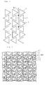
- FIG. 3 In a plan view of Fig. 3 , the arrangement of projections 1 in a sapphire substrate according to Embodiment 2 of the present invention is shown.
- the arrangement of Fig. 3 is composed of a plurality of rows that are respectively constituted by a plurality of projections 1.
- the plurality of projections 1 arranged in the same row are respectively arranged so that bisectors that bisect an angle of one of vertexes of the projections is located on a straight line and also the projection direction defined by the direction, in which the bisector faces outside from the inside of projections 1, becomes the same.
- the arrangement direction of projections 1 of odd numbered rows is opposite to the arrangement direction of projections 1 of even numbered rows.
- the direction of projections 1 in each row is opposite between adjacent projections.
- the size of a bottom of the respective projections 1 is set so that a straight line passes through the inside of any one of projections 1 even if the straight line is drawn at any position in parallel to the row and the straight line is drawn at any position in parallel to the column.
- a sapphire substrate including a plurality of projections 1 having the size set as described above and arranged as shown in Fig. 3
- a semiconductor laminated structure 20 in which a base layer 21, a first conductive layer (n-type layer) 22, an active layer (emissive layer) 23 and a second conductive layer (p-type layer) 24 are sequentially formed on one principal surface on which plurality of projections 1 are formed, is constituted and thus a nitride semiconductor light emitting device is constituted, light emitted toward the sapphire substrate side among light emitted in the emissive layer 23 is reflected by at least one of projections 1, even if light L1, that propagates in parallel and proximal to the surface of the substrate located between adjacent projections 1, propagates in any direction.
- the nitride semiconductor light emitting device constituted using the sapphire substrate of the present Embodiment 2 enables light to efficiently reflect in the light emission direction without being emitted from the side by the presence of the above arranged plurality of projections 1, and thus light extraction efficiency can be increased.
- projections 1 are arranged comparatively densely by the above arrangement and the area occupied by the bottom of the plurality of projections 1 provided on one principal surface based on the entire one principal surface of the sapphire substrate increases, and thus enabling the growth of a nitride semiconductor with low dislocation, resulting in high luminous efficiency of the nitride semiconductor light emitting device.
- a group G1 composed of six projections 1 as a plurality of projections 1, arranged so that a gravity center of a bottom of each projection agrees with a vertex and a center of regular pentagon, is repeatedly arranged in accordance with a fixed rule.
- Regular pentagon is arranged so that the center of each regular pentagon agrees with a vertex of a triangular lattice point, and also projections 1 are separated and do not overlap between adjacent groups G1. Furthermore, regarding the size of each projection 1, the size of the bottom of each projection 1 is set so that a straight line passes through the inside of any one of projections 1 when the straight line is optionally drawn on one principal surface.
- a sapphire substrate including a plurality of projections 1 having the size set as described above and arranged as shown in Fig. 4
- a semiconductor laminated structure 20 in which a base layer 21, a first conductive layer (n-type layer) 22, an active layer (emissive layer) 23 and a second conductive layer (p-type layer) 24 are sequentially formed on one principal surface on which plurality of projections 1 are formed, is constituted and thus a nitride semiconductor light emitting device is constituted, light emitted on the sapphire substrate side among light emitted in the emissive layer 23 is reflected by at least one of projections 1, even if light L1, that propagates in parallel and proximal to the surface of the substrate located between adjacent projection 1, propagates in any direction.
- the nitride semiconductor light emitting device constituted using the sapphire substrate of the present Embodiment 3 enables light to efficiently reflect in the light emission direction without being emitted from the side by the presence of the above arranged plurality of projections 1, and thus light extraction efficiency can be increased.
- projections 1 are arranged comparatively densely by the above arrangement and the area occupied by the bottom of the plurality of projections 1 provided on one principal surface based on the entire one principal surface of the sapphire substrate increases, and thus enabling the growth of a nitride semiconductor with low dislocation, resulting in high luminous efficiency of the nitride semiconductor light emitting device.
- a plan view of Fig. 5 the arrangement of projections 1 in a sapphire substrate according to the embodiment 4 of the present invention is shown.
- the sapphire substrate of the present Embodiment 4 is the same as in Embodiment 3 in that it includes a plurality of groups G1 composed of six projections 1 arranged on the vertex and center of regular pentagon, but is different in the rule when the group G1 is repeatedly arranged. That is, in the sapphire substrate of Embodiment 4, as shown in Fig. 5 , a plurality of groups G1 arranged in the first row (uppermost row in the drawing) are juxtaposed so that all regular pentagons, that determine the arrangement of projections 1, have the same direction.
- a plurality of groups G1 arranged in the subsequent second row are juxtaposed so that regular pentagon, that determines the arrangement of each group G1, faces opposite to regular pentagon, that determines the arrangement of the group G1 arranged in the first row, relative to the group G1 arranged in the first row.
- the arrangement position of the group G1 arranged in the first row and that of the group G1 arranged in the second row are set so that the center of regular pentagon, that determines the arrangement of the group G1 arranged in the first row, and the center of regular pentagon, that determines the arrangement of the group G1 arranged in the second row, are located at the vertexes of triangular lattice. Furthermore, as shown in Fig.
- the arrangement in the third row and that of the fourth row are set so that the third row and the fourth row become linear symmetry.
- the arrangement of projections 1 in the sapphire substrate of Embodiment 4 is set by repeating the arrangement similar to that in the first row to fourth row.
- the size of the bottom of each projection 1 is set so that a straight line passes through the inside of a bottom of at least one of projections 1 when the straight line is optionally drawn on one principal surface.
- the nitride semiconductor light emitting device thus constituted using a sapphire substrate of the present Embodiment 4 including a plurality of projections 1 having the size set as described above and arranged as shown in Fig. 5 enables light to efficiently reflect in the light emission direction without being emitted from the side by a plurality of projections 1, and thus light extraction efficiency can be increased.
- projections 1 are arranged comparatively densely by the above arrangement and the area occupied by the bottom of the plurality of projections 1 provided on one principal surface based on the entire one principal surface of the sapphire substrate increases, and thus enabling the growth of a nitride semiconductor with low dislocation, resulting in high luminous efficiency of the nitride semiconductor light emitting device.
- a group G1 composed of six projections 1 as a plurality of projections 1 arranged so that a gravity center of a bottom of each projection agrees with a vertex and a center of regular pentagon is repeatedly arranged in accordance with a fixed rule that is different from in Embodiments 3 and 4.
- the group G1 arranged in the same column is arranged in the same direction without rotating, and the group G1 is arranged in a reverse direction between adjacent columns.
- the group G1 arranged in even numbered columns is arranged slightly downward as compared with the group G1 arranged in odd numbered columns.
- the direction of the group G1 arranged in each row becomes reverse between adjacent rows, and a line connecting centers of regular pentagons, that determine the arrangement of the group G1 in each row, becomes a bent line (zigzag line).
- the size of the bottom of each projection 1 is set so that a straight line passes through the inside of any one of projections 1 when the straight line is optionally drawn on a plane including a bottom of projection 1.
- a sapphire substrate including a plurality of projections 1 having the size set as described above and arranged as shown in Fig. 6
- a semiconductor laminated structure 20 in which a base layer 21, a first conductive layer (n-type layer) 22, an active layer (emissive layer) 23 and a second conductive layer (p-type layer) 24 are sequentially formed on one principal surface on which plurality of projections 1 are formed, is constituted and thus a nitride semiconductor light emitting device is constituted, light emitted on the sapphire substrate side among light emitted in the emissive layer 23 is reflected by at least one of projections 1, even if light L1, that propagates in parallel and proximal to the surface of the substrate located between adjacent projection 1, propagates in any direction.
- the nitride semiconductor light emitting device constituted using the sapphire substrate of the present Embodiment 5 enables light to efficiently reflect in the light emission direction without being emitted from the side by the presence of the plurality of projections 1, and thus light extraction efficiency can be increased.
- the area occupied by the bottom of the plurality of projections 1 provided on one principal surface based on the entire one principal surface of the sapphire substrate increases, and thus enabling the growth of a nitride semiconductor with low dislocation, resulting in high luminous efficiency of the nitride semiconductor light emitting device.
- a group G10 which is composed of eight projections 1 as a plurality of projections 1 arranged respectively on vertexes of regular octagon, and projections 2 composed of projections larger than the projections 1 arranged on the center of regular octagon, is repeatedly arranged in accordance with a fixed rule.
- the group G10 is repeatedly arranged in two directions of a row and a column, that intersect with each other, and respectively shares two projections 1 between adjacent two groups G10 in the same row and between adjacent two groups G10 in the same column.
- the size of each projection 1 and the size of each projection 2 are set so that a straight line passes through the inside of projections 1 or projections 2 when the straight line is optionally drawn on one principal surface including a bottom of projections 1.
- a sapphire substrate including projections 1 and projections 2, each having the size set as described above, and also including a plurality of projections 1 arranged as shown in Fig. 7
- a semiconductor laminated structure 20 in which a base layer 21, a first conductive layer (n-type layer) 22, an active layer (emissive layer) 23 and a second conductive layer (p-type layer) 24 are sequentially formed on one principal surface on which plurality of projections 1 are formed, is constituted and thus a nitride semiconductor light emitting device is constituted, light emitted toward the sapphire substrate side among light emitted in the emissive layer 23 is reflected by at least one of projections 1, even if light L1, that propagates in parallel and proximal to the surface of the substrate located between adjacent projections 1, propagates in any direction.
- the nitride semiconductor light emitting device constituted using the sapphire substrate of the present Embodiment 6 enables light to efficiently reflect in the light emission direction without being emitted from the side by the plurality of projections 1 and projections 2, and thus light extraction efficiency can be increased.
- the area occupied by the bottom of the plurality of projections 1 provided on one principal surface based on the entire one principal surface of the sapphire substrate increases, and thus enabling the growth of a nitride semiconductor with low dislocation, resulting in high luminous efficiency of the nitride semiconductor light emitting device.
- a bottom and a top surface of projections of Embodiment 7 have a truncated triangular pyramidal shape modified as described hereinafter. Therefore, it is possible to easily realize the arrangement of a plurality of projections 1, that enables light to be effectively reflected by projections 1, even if light L1, that propagates in parallel and proximal to a surface of the substrate, propagates in any direction, and thus light extraction efficiency can be improved.
- the bottom of projections of Embodiment 7 has a substantially triangular shape in which each of sides 11, 12, 13 include a depression in the center.
- the side 11 is respectively composed of outwardly bulged two curved lines 11a, 11b, and a depression is formed at the connection portion thereof.
- the side 12 is respectively composed of outwardly bulged two curved lines 12a, 12b, and a depression is formed at the connection portion thereof.
- the side 13 is respectively composed of outwardly bulged two curved lines 13a, 13b, and a depression is formed at the connection portion thereof.
- the top surface of projections 1 of Embodiment 7 also has a substantially triangular shape, that is almost similar to that of the bottom including a depression in the center of each side.
- projections 1 constituted as described above are arranged so that, in adjacent two projections, one of vertexes of a bottom of one projection 1 is located (enter into) in a proximal region defined by connecting points of two vertexes of a bottom of the other projection 1 and the deepest point of a depression existing therebetween.
- a straight line necessarily passes through the inside of any one of projections 1 when the straight line is drawn at any position in any direction in a plane including a bottom of projections 1.
- each of projections 1 has a shape with linear symmetry to a straight line that connects a depression and a vertex opposite to the side including the depression, and thus the above arrangement can be easily realized.
- a nitride semiconductor light emitting device is constituted using a sapphire substrate of Embodiment 7 in which the shape and the arrangement of projections 1 are set as described above, it is possible to reflect by projections 1 even if light L1, that propagates in parallel and proximal to a surface of the substrate, propagates in any direction. Accordingly, the nitride semiconductor light emitting device constituted using a sapphire substrate of the present Embodiment 7 enables light to efficiently reflect in the light emission direction without being emitted from the side by a plurality of projections 1, and thus light extraction efficiency can be increased.
- An area occupied by the bottom of the plurality of projections 1 provided on one principal surface in the entire one principal surface in the sapphire substrate of the present Embodiment 7 increases, and thus enabling the growth of a nitride semiconductor with low dislocation, resulting in high luminous efficiency of the nitride semiconductor light emitting device.
- the height of the projection 1 can be decreased as compared with the projection having a triangular pyramidal shape. Therefore, it becomes possible to supply a raw gas, almost uniformly, to a growth surface (surface of a sapphire substrate located between projections 1) of a nitride semiconductor layer when a base layer 21 is grown on one principal surface on which a plurality of projections 1 are formed. Whereby, it becomes possible to perform growth in a lateral direction, that uniformly covers projections 1 from the growth surface of a nitride semiconductor layer. Also, because the height of projections 1 is decreased, a flat surface is obtained by a comparatively thin base layer 21.
- Projections 1 having a petal shape in the present Embodiment 7 can be formed by setting a crystal form, crystal orientation of a surface of a substrate on which projections 1 are formed, mask shape and size, and etching conditions according to the objective shape.
- Fig. 8 an example of a mask M1 in case of forming projections 1 shown in Fig. 9 on a C-plane of a sapphire substrate is shown.
- the mask M1 of this example is composed of three legs (tripod shape), each having the same length and the same width, extending in three directions for every 120 degrees from the center.
- a top surface 1b of projections 1 is formed, under the mask M1, into the shape in which the shape of the mask M1 is modified, and an inclined side 1a is formed from an end of the top surface of projections 1.
- the shape of the top surface of projections 1 becomes a shape in which the tripod shape of the mask M1 is modified to reflect etching characteristics, by an influence of a direction dependence of an etching rate due to a crystal form.
- the shape becomes a substantially triangular shape that includes a depression in the center of each side and also includes a sharpened vertex.
- the bottom of projections 1 also becomes a substantially triangular shape, that is almost similar to the shape of a top surface including a depression in the center of each side and also including a sharpened vertex, in which the tripod shape of the mask M1 is modified depending on etching characteristics.
- a ridge 1r connecting a vertex of the top surface to a vertex of the bottom, and a valley 12c connecting the deepest portion of a depression of the bottom to the deepest portion of a depression of the top surface are formed on the inclined side between the bottom and the top surface.
- a ridge 1r protruding outwardly from a leg tip is formed at the tip portion (leg tip) of the leg of the mask M1, and inclined surfaces, each having a different inclination direction, are formed on both sides of the ridge 1r.
- a plurality of masks M1 are formed so that a leg tip of one leg of one mask M1 is proximal to or agrees with a straight line that connects corners of two leg tips of another mask M1 that is adjacent to said one mask M1, whereby, a plurality of projections 1 are arranged so that one of vertexes of a bottom of one projection 1 is located (enter into) in a proximal region defined by connecting two vertexes and the deepest point of a depression, existing therebetween, of a bottom of another projection 1 that is adjacent to said one projection.
- a direction of projections 1 can be set to the desired direction by changing an off angle from a C-plane of a surface of a sapphire substrate on which projections 1 are formed.
- projections each having a substantially polygonal pyramidal shape (particularly, substantially triangular pyramidal shape) whose bottom has a substantially polygonal shape (particularly, substantially triangular shape), were described in the above Embodiments 1 to 7, the present invention is not limited thereto.
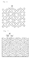
- the projections may be either projections 31 whose bottom shape has a dogleg shape bent in the center as shown in Fig. 10 , or projections 32 whose bottom shape has a cross shape as shown in Fig. 11 . According to projections 31 whose bottom shape has a dogleg shape shown in Fig.
- a plurality of projections 31 can be arranged so that a straight line passes through the inside of at least one of projections 31 when the straight line is drawn at any position in any direction on a surface of sapphire substrate on which projections 31 are formed.
- projections 32 Fig. 11
- a plurality of projections 32 can be arranged so that a straight line passes through the inside of at least any one of projections 32 when the straight line is drawn at any position in any direction on a surface of sapphire substrate on which projections 32 are formed.
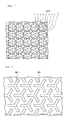
- a plan view of Fig. 12 the shape and the arrangement of projections 40 in a sapphire substrate according to Embodiment 8 of the present invention are shown.
- Projections 40 of Embodiment 8 are formed in a direction in which projections 1 of Embodiment 7 are rotated by 180 degrees.
- the direction of projections is defined on the basis of an orientation flat (A-plane) 100 of a sapphire substrate as shown in Fig. 15 .
- both projections 40 of Embodiment 8 and projections 1 of Embodiment 7 are formed so that the direction of projections (three directions from the center toward the vertex of a substantially triangular shape in a bottom of the substantially triangular shape) and an a-axis intersect with each other, but the direction of projections is opposite.
- the above three directions in projections 1 of Embodiment 7 agree with directions that are rotated counter clockwise (left-handed) by 30 degrees from the a-axes (axis a1, axis a2 and axis a3) as shown in Fig.
- Projections 40 of Embodiment 8 in which projections 1 are rotated by 180 degrees can be formed by forming a mask M45 extending in three directions that agree with the above three directions shown in Fig. 13 on a C-plane of a sapphire substrate, followed by etching.
- a mask M45 extending in three directions that agree with the above three directions shown in Fig. 13 on a C-plane of a sapphire substrate, followed by etching.
- the surface to be etched in the direction parallel to the a-axis makes an obtuse angle with the C-plane
- the surface to be etched in a vertical direction makes an acute angle with the C-plane. Therefore, the shape of projections 40 formed by etching becomes the shape that is different from that of projections 1, as described hereinafter.
- the thus formed projections 40 of Embodiment 8 are the same as projections 1 of Embodiment 7 in that a bottom has a substantially triangular shape and also each side of a bottom thereof includes a depression in the center. As is apparent from a comparison between Fig. 9 and Fig. 12 , the proportion occupied by the inclined side 40a to the entire surface area in projections 40 increases and the proportion occupied by the top surface 40b relatively decreases.
- an outer periphery shape of a protruded portion of one projection 40 has the same shape as that of the depressed side of the other projection 40, and a C-plane of a sapphire substrate is formed in almost the same width between the protruded portion of one projection 40 and the depressed side of the other projection 40.
- the C-plane of a sapphire substrate between three projections 1 extends in a substantially triangular shape in Embodiment 7
- the C-plane of a sapphire substrate located between three projections 40 is formed in almost the same width and becomes narrow in Embodiment 8.
- projections 40 of Embodiment 8 can widen an area of a bottom of projections 40 as compared with an area of a bottom of projections 1 of Embodiment 7. As a result, an area of the C-plane of a sapphire substrate between projections 40 can be decreased.
- the proportion of the nitride semiconductor grown in a lateral direction can be increased and dislocation of the grown nitride semiconductor can be decreased.
- each side of a bottom of projections 40 respectively includes a depression in the center and can be arranged so that a straight line passes through the inside of at least one of projections 32 when the straight line is drawn at any position in any direction on a surface of the sapphire substrate.
- the proportion of the nitride semiconductor grown in a lateral direction can be increased and dislocation of the grown nitride semiconductor can be decreased.
- the above three directions in projections 40 were set to agree with directions that are rotated clockwise (right-handed) by 30 degrees from the a-axes (axis a1, axis a2 and axis a3).
- the present invention is not limited thereto.
- the above three directions in projections 40 are adjusted within a range of ⁇ 10 degrees of the directions that are rotated clockwise by 30 degrees from the a-axes, the same operation and effect as in Embodiment 8 can be obtained.
- a plan view of Fig. 14 the shape and the arrangement of projections 50 in a sapphire substrate according to Embodiment 9 of the present invention are shown.
- Projections 50 in the sapphire substrate of Embodiment 9 are formed in the direction in which projections 1 of Embodiment 7 are rotated by 180 degrees, similar to projections 40 of Embodiment 8.
- the constitution of a top surface 50b of projections 50 is different from that of a top surface 40b of projections 40 of Embodiment 8.
- the top surface 50b of Embodiment 9 is depressed in the center of projections 50 and the top surface 50b is a surface inclined from the sapphire C-plane.
- the area of a C-plane of a sapphire substrate between projections 50 can be decreased by increasing the proportion of the inclined side 50a of projections 50, and further the growth of a nitride semiconductor on the top surface 50b of projections 50, which is a surface inclined from the sapphire C-plane can be suppressed.
- the sapphire substrate of Embodiment 9 can further decrease the area occupied by a C-plane based on the entire one principal surface, and thus enabling the growth of a nitride semiconductor with less threading dislocation.
- a top surface 50b of projections 50 when at least a part, preferably entirety of a top surface 50b of projections 50 is a surface that is not a sapphire C-plane, the growth of a nitride semiconductor on the top surface 50b is suppressed, and thus the generation of pores (voids) can be suppressed.
- Projections 50 including the top surface 50b composed of a surface that is not a sapphire C-plane can be produced by appropriately adjusting the mask shape.
- an interval between masks may be appropriately adjusted.
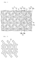
- FIG. 16A In a plan view of Fig. 16A , the shape and the arrangement of projections 60 in a sapphire substrate according to Embodiment 10 of the present invention are shown.
- Fig. 16B projections 60 of Fig. 16A are enlargely shown.
- projections 60 include an inclined side 60a and a top surface 60b.
- projections 60 are formed in a direction in which projections 1 of Embodiment 7 are rotated clockwise by 30 degrees. That is, as shown in Fig. 18(a) and Fig.
- projections 60 of Embodiment 10 are formed so that three directions from the center toward the vertex in a bottom of projections 60, each having a substantially triangular shape, agree with the a-axis.
- a plurality of projections 60 are arranged in the direction that agrees with the a-axis.
- Projections 60 can be formed by forming a mask M65, in which three directions from the center toward the tip agree with the a-axis on a C-plane of a sapphire substrate, in the direction that agrees with the a-axis, followed by etching.
- the sapphire substrate is etched using the mask M65 thus formed, the direction that is easily etched and the direction that is less easily etched are formed (etching anisotropy appears). Therefore, as shown in Fig. 16A and Fig. 16B , a width A of an inclined side becomes larger than a width B of the other inclined side at one side of the a-axis, and thus an area of the inclined side 60a increases.
- an area of a C-plane of a sapphire substrate formed between projections 60 can be decreased, and thus threading dislocation in case of growing a nitride semiconductor can be decreased.
- the nitride semiconductor to be grown on a sapphire C-plane slowly grows in the direction of the a-axis and quickly grows in the direction rotated from the a-axis by 30 degrees, as shown in Fig. 18(d) .
- the nitride semiconductor in the direction that intersects with the a-axis grows more quickly.
- the extended portion extending in the direction that agrees with the a-axis of projections 60 is quickly covered with the nitride semiconductor grown from both sides thereof ( Fig. 18(c) ).
- the above three directions in projections 60 was allowed to agree with the a-axis.
- the present invention is not limited thereto.
- the same operation and effect as in Embodiment 10 can be obtained by adjusting the above three directions in projections 60 within a range of the a-axis ⁇ 10 degrees.
- Projections 70 in the sapphire substrate of Embodiment 11 is composed of a subprojection 70s1, a subprojection 70s2 and a subprojection 70s3 in the form where projections 1 having a petal shape in Embodiment 7 are separated in the center.
- projections 70 are separated in the center, the portion of a triangular shape through which light is capable of going straight is formed between subprojections 70s1, 70s2, 70s3 on one principal surface of the sapphire substrate of Embodiment 11.
- three subprojections 70s1, 70s2, 70s3 are proximal to each other.
- projections 70 in Embodiment 11 similar to projections 1, each having a petal shape in Embodiment 7, projections 70 can be arrange so that a straight line passes through the inside of at least one of projections 70 when the straight line is drawn at any position in any direction on a surface of a sapphire substrate on which projections 70 are formed.
- Projections 70 separated in the center can be formed by forming a mask M70 composed of masks M70a1, M70a2, M70a3 separated in the center as shown in Fig. 20 in the predetermined arrangement and etching a sapphire substrate.
- the shape of the portion to be separated can be adjusted by a shape of tip portions facing each other of masks M70a1, M70a2, M70a3 as shown in Fig. 20 .
- projections 70 separated into subprojections 70s1, 70s2, 70s3 are formed on one principal surface.
- Projections 80 in the sapphire substrate of Embodiment 12 is composed of a subprojection 80s1, a subprojection 80s2 and a subprojection 80s3 in the form where projections 40 having a petal shape in Embodiment 8 are separated in the center.
- the gap through which light is capable of going straight is formed between subprojections 80s1, 80s2, 80s3 on one principal surface of the sapphire substrate of Embodiment 12.
- three subprojections 80s1, 80s2, 80s3 are proximal to each other.
- projections 80 in Embodiment 12 similar to projections 40 each having a petal shape in Embodiment 8, projections 80 can be arrange so that a straight line passes through the inside of at least one of projections 80 when the straight line is drawn at any position in any direction on a surface of a sapphire substrate on which projections 40 are formed.
- Projections 80 separated in the center can be formed by forming a mask M80 composed of masks M80a1, M80a2, M80a3 separated in the center as shown in Fig. 22 in a predetermined arrangement and etching a sapphire substrate.
- the reason why the shape of the portion to be separated is different from that in Embodiment 11 shown in Fig. 19 is due to direction anisotropy of an etching rate of the sapphire substrate since projections 80 of Embodiment 12 are formed in the direction in which projections 70 of Embodiment 11 are rotated by 180 degrees.
- projections 80 separated into subprojections 80s1, 80s2, 80s3 are formed on one principal surface.
Landscapes
- Led Devices (AREA)
- Chemical & Material Sciences (AREA)
- Crystallography & Structural Chemistry (AREA)
Abstract
Description
- The present invention relates to a sapphire substrate for a nitride semiconductor light emitting device, and a semiconductor light emitting device.
- For example, a light emitting diode (LED) made of a nitride semiconductor is usually constituted by sequentially laminating an n-type semiconductor layer, an active layer and a p-type semiconductor layer on a sapphire substrate. In this light emitting diode, emitted light is extracted from the side opposite the sapphire substrate or the side of the sapphire substrate, while light emitted from the active layer is also radiated in a direction opposite the light emission side. Therefore, it becomes necessary to improve external quantum efficiency by enabling light radiated in a direction opposite the light emission side to extract effectively from the light emission side.
- For example,
Patent Document 1 discloses that external quantum efficiency is improved by arranging a plurality of projections having truncated triangular pyramid-shaped on a sapphire substrate.Patent Document 1 also describes that generation of voids and deterioration of crystallinity can be suppressed by enabling crystal growth on a surface, on which projections having a truncated triangular pyramidal shape are formed, through the projections. - Patent Document 1:
JP-A-2008-177528 - However, the present inventors have intensively studied and found that, in a light emitting diode composed of a nitride semiconductor grown on a surface including projections having a truncated triangular pyramidal shape, it was not necessarily possible that light emitted in the direction opposite the light emission side is efficiently extracted from the light emission side, and external quantum efficiency is sufficiently improved.
- Thus, an object of the present invention is to provide a sapphire substrate for a nitride semiconductor light emitting device, that can constitute a nitride semiconductor light emitting device having excellent light extraction efficiency.
Another object of the present invention is to provide a semiconductor light emitting device having excellent light extraction efficiency. - In order to achieve the above objects, the sapphire substrate according to the present invention is a sapphire substrate having a principal surface for growing a nitride semiconductor to form a nitride semiconductor light emitting device and comprising a plurality of projections on the principal surface, wherein an outer periphery of a bottom of each of the projections has at least one depression. This depression does not mean a depression in a vertical direction to a sapphire substrate, but means a depression in a horizontal direction.
- The plurality of projections are arranged so that a straight line passes through the inside of at least one of projections when the straight line is drawn at any position in any direction in a plane including the bottoms of the plurality of projections.
The projections have a substantially polygonal pyramidal shape or substantially truncated polygonal pyramidal shape whose bottom has a substantially polygonal shape, respectively, and each side of the bottom includes a depression in the center. - The semiconductor light emitting device according to the present invention is characterized in that a nitride semiconductor light emitting device is formed by growing a nitride semiconductor layer on one principal surface of the sapphire substrate according to the present invention.
- The sapphire substrate constituted as described above according to the present invention has a principal surface comprising a plurality of projections for growing a nitride semiconductor to form a nitride semiconductor light emitting device and an outer periphery of a bottom of each of the projections has at least one depression. Therefore, light emitted in parallel to the sapphire substrate on a surface thereof is irradiated on projections, and thus it is possible to provide a sapphire substrate for a nitride semiconductor light emitting device, that can constitute a nitride semiconductor light emitting device having excellent light extraction efficiency.
In the sapphire substrate, the plurality of projections are arranged so that a straight line passes through the inside of at least one of projections when the straight line is drawn at any position in any direction in a plane including a bottom of the plurality of projections. Therefore, when a nitride semiconductor light emitting device is constituted on one principal surface, light, that propagates in parallel and proximal to one principal surface, is reflected by at least one of projections even if light propagates in any direction.
Accordingly, the sapphire substrate according to the present invention can provide a sapphire substrate for a nitride semiconductor light emitting device, that can constitute a nitride semiconductor light emitting device having excellent light extraction efficiency. - In the sapphire substrate, each of the projections has a substantially polygonal pyramidal shape or substantially truncated polygonal pyramidal shape whose bottom has a substantially polygonal shape, and each side of the bottom includes a depression in the center. Therefore, it is possible to easily realize the arrangement of projections so that a straight line passes through the inside of at least one of projections when the straight line is drawn at any position in any direction in a plane including a bottom of the plurality of projections,.
- In the light emitting device according to the present invention, a nitride semiconductor light emitting device is formed by growing a nitride semiconductor layer on one principal surface of the sapphire substrate according to the present invention. Therefore, it is possible to provide a semiconductor light emitting device having excellent light extraction efficiency.
-
-
Fig. 1 is a sectional view of a nitride semiconductor light emitting device according to the embodiment of the present invention. -
Fig. 2 is a plan view showing the arrangement of projections in a sapphire substrate according toEmbodiment 1 of the present invention. -
Fig. 3 is a plan view showing the arrangement of projections in a sapphire substrate according toEmbodiment 2 of the present invention. -
Fig. 4 is a plan view showing the arrangement of projections in a sapphire substrate according toEmbodiment 3 of the present invention. -
Fig. 5 is a plan view showing the arrangement of projections in a sapphire substrate according to Embodiment 4 of the present invention. -
Fig. 6 is a plan view showing the arrangement of projections in a sapphire substrate according to Embodiment 5 of the present invention. -
Fig. 7 is a plan view showing the arrangement of projections in a sapphire substrate according to Embodiment 6 of the present invention. -
Fig. 8 is a plan view showing an example of a mask used when projections according to Embodiment 7 of the present invention is formed on a sapphire substrate. -
Fig. 9 is a plan view showing the constitution and arrangement of projections in a sapphire substrate according to Embodiment 7 of the present invention. -
Fig. 10 is a plan view showing the constitution and arrangement of projections in a sapphire substrate according toVariation 1 of the present invention. -
Fig. 11 is a plan view showing the constitution and arrangement of projections in a sapphire substrate according toVariation 2 of the present invention. -
Fig. 12 is a plan view showing the constitution and arrangement of projections in a sapphire substrate according to Embodiment 8 of the present invention. -
Fig. 13 is a plan view of a mask used when projections according to Embodiment 8 of the present invention is formed on a sapphire substrate. -
Fig. 14 is a plan view showing the constitution and arrangement of projections in a sapphire substrate according to Embodiment 9 of the present invention. -
Fig. 15(a) is a plan view showing an orientation flat (A-plane) and a crystal axis (a-axis) of a sapphire wafer, andFig. 15(b) is a plan view showing a direction of projections. -
Fig. 16A is a plan view showing the constitution and arrangement of projections in a sapphire substrate according toEmbodiment 10 of the present invention. -
Fig. 16B is a plan view enlargely showing the constitution of projections ofEmbodiment 10. -
Fig. 17 is a plan view showing an example of a mask used when projections according toEmbodiment 10 of the present invention is formed on a sapphire substrate. -
Fig. 18(a) is a plan view showing an orientation flat (A-plane) and a crystal axis (a-axis) of a sapphire wafer,Figs. 18 (b) and 18(c) are plan views schematically showing a direction of projections and a growth rate of a nitride semiconductor, andFig. 18(d) is a schematic view showing crystal orientation dependence of sapphire of a growth rate of a nitride semiconductor. -
Fig. 19 is a plan view showing the constitution and arrangement of projections in a sapphire substrate according to Embodiment 11 of the present invention. -
Fig. 20 is a plan view of a mask used when projections according toEmbodiment 11 of the present invention is formed on a sapphire substrate. -
Fig. 21 is a plan view showing the constitution and arrangement of projections in a sapphire substrate according to Embodiment 12 of the present invention. -
Fig. 22 is a plan view of a mask used when projections according toEmbodiment 12 of the present invention is formed on a sapphire substrate. - As shown in
Fig. 1 , the nitride semiconductor light emitting device according to the embodiment of the present invention is provided with a semiconductor laminatedstructure 20 in which abase layer 21, a first conductive layer (n-type layer) 22, an active layer (emissive layer) 23 and a second conductive layer (p-type layer) 24 are sequentially laminated on asapphire substrate 10, and a plurality of projections (dimples) 1, each having a pyramidal shape or a truncated pyramidal shape, are provided on a surface of thesubstrate 10 on which thebase layer 21 is grown.
Herein, particularly in the present embodiment, a plurality ofprojections 1 are arranged so that light, that propagates in parallel and proximal to the surface of the substrate located betweenadjacent projections 1, is reflected by at least one of projections even if light propagates in any direction.
Whereby, the nitride semiconductor light emitting device of the present embodiment, by having a plurality ofprojections 1, enables light emitted in the emissive layer 23 to efficiently reflect in the light emission direction without being emitted from the side, and thus light extraction efficiency can be increased.
Specific arrangement example ofprojections 1 in a sapphire substrate according to the embodiment of the present invention will be described below. - In the present invention, the
projection 1 may have a substantially n-sided pyramidal shape, or a substantially truncated n-sided pyramidal shape including atop surface 1b that is substantially parallel to a bottom and has a shape substantially similar to that of the bottom, and each bottom may have a substantially n-sided polygon shape including n sides, each having an outwardly bulged arc shape. In the following descriptions ofEmbodiments 1 to 6, description is made using an example of theprojection 1 having a typical substantially triangular pyramidal shape or a substantially truncated triangular pyramidal shape.
In the drawings to be referred inEmbodiments 1 to 6, a planar shape (a shape of a bottom) of theprojection 1 is schematically shown by regular triangle. When aprojection 1 having a substantially triangular pyramidal shape or a substantially truncated triangular pyramidal shape is formed by etching a sapphire substrate, each side of a bottom thereof usually becomes a side having an outwardly bulged arc shape and an inclined side of theprojection 1 becomes an outwardly bulged surface. - In a plan view of
Fig. 2 , the arrangement ofprojections 1 in a sapphire substrate according to theembodiment 1 of the present invention is shown.
In thepresent Embodiment 1, a plurality ofprojections 1, each having a substantially triangular pyramidal shape, are arranged so that a gravity center of a bottom agrees with each lattice point of a triangular lattice having a lattice shape of regular triangle. InEmbodiment 1,projections 1 are arranged on the lattice point of a triangular lattice so that allprojections 1 face the same direction. In the present description, the direction ofprojections 1 refers to the direction in which a line, that bisect an angle of a vertex of a bottom, faces outside from the inside ofprojections 1, and two ormore projections 1 facing the same direction refers that all directions corresponding betweenprojections 1 face the same direction. In other words, it refers that projections are arranged in a state where projections can be superposed on a bottom of other allprojections 1 by parallel translation without rotating the bottom.
The plurality ofprojections 1 thus arranged ofEmbodiment 1 are arranged so as to form a plurality of rows, and are respectively arranged so that bisectors that bisect an angle of one of vertexes ofprojections 1 arranged in the same line is located on a straight line, and also the projection direction defined by the direction, in which the bisector faces outside from the inside ofprojections 1, becomes the same, even in case of looking at the row in any direction. - In the
present Embodiment 1, in addition to the above arrangement, the size ofprojections 1 is set so that a straight line necessarily passes through the inside of any one ofprojections 1 when the straight line is drawn at any position in any direction in the plane including a bottom ofprojections 1. - Using a sapphire substrate including a plurality of
projections 1 having the size set as described above and arranged as shown inFig. 2 , when a semiconductorlaminated structure 20, in which abase layer 21, a first conductive layer (n-type layer) 22, an active layer (emissive layer) 23 and a second conductive layer (p-type layer) 24 are sequentially formed on one principal surface on which plurality ofprojections 1 are formed, is constituted and thus a nitride semiconductor light emitting device is constituted, light emitted toward the sapphire substrate side among light emitted in the emissive layer 23 is reflected by at least one ofprojections 1, even if light L1, that propagates in parallel to the surface of the substrate located betweenadjacent projections 1 and proximal to the surface of the substrate, propagates in any direction.
Accordingly, the nitride semiconductor light emitting device constituted using the sapphire substrate of thepresent Embodiment 1 enables light to efficiently reflect in the light emission direction without being emitted from the side by the presence of the above arranged plurality ofprojections 1, and thus light extraction efficiency can be increased. - In the sapphire substrate of the
present Embodiment 1,projections 1 are arranged comparatively densely by the above arrangement and the proportion occupied by the plurality ofprojections 1 provided on one principal surface based on the entire one principal surface of the sapphire substrate increases, and thus enabling the growth of a nitride semiconductor with low dislocation, resulting in high luminous efficiency of the nitride semiconductor light emitting device. - In a plan view of
Fig. 3 , the arrangement ofprojections 1 in a sapphire substrate according toEmbodiment 2 of the present invention is shown.
The arrangement ofFig. 3 is composed of a plurality of rows that are respectively constituted by a plurality ofprojections 1. The plurality ofprojections 1 arranged in the same row are respectively arranged so that bisectors that bisect an angle of one of vertexes of the projections is located on a straight line and also the projection direction defined by the direction, in which the bisector faces outside from the inside ofprojections 1, becomes the same. The arrangement direction ofprojections 1 of odd numbered rows is opposite to the arrangement direction ofprojections 1 of even numbered rows. That is, the direction ofprojections 1 in each row is opposite between adjacent projections.
The size of a bottom of therespective projections 1 is set so that a straight line passes through the inside of any one ofprojections 1 even if the straight line is drawn at any position in parallel to the row and the straight line is drawn at any position in parallel to the column. - Using a sapphire substrate including a plurality of
projections 1 having the size set as described above and arranged as shown inFig. 3 , when a semiconductorlaminated structure 20, in which abase layer 21, a first conductive layer (n-type layer) 22, an active layer (emissive layer) 23 and a second conductive layer (p-type layer) 24 are sequentially formed on one principal surface on which plurality ofprojections 1 are formed, is constituted and thus a nitride semiconductor light emitting device is constituted, light emitted toward the sapphire substrate side among light emitted in the emissive layer 23 is reflected by at least one ofprojections 1, even if light L1, that propagates in parallel and proximal to the surface of the substrate located betweenadjacent projections 1, propagates in any direction.
Accordingly, the nitride semiconductor light emitting device constituted using the sapphire substrate of thepresent Embodiment 2 enables light to efficiently reflect in the light emission direction without being emitted from the side by the presence of the above arranged plurality ofprojections 1, and thus light extraction efficiency can be increased. - In the sapphire substrate of the
present Embodiment 2,projections 1 are arranged comparatively densely by the above arrangement and the area occupied by the bottom of the plurality ofprojections 1 provided on one principal surface based on the entire one principal surface of the sapphire substrate increases, and thus enabling the growth of a nitride semiconductor with low dislocation, resulting in high luminous efficiency of the nitride semiconductor light emitting device. - In a plan view of
Fig. 4 , the arrangement ofprojections 1, each having a substantially triangular pyramidal shape, in a sapphire substrate according toEmbodiment 3 of the present invention is shown. In thepresent Embodiment 3, a group G1 composed of sixprojections 1 as a plurality ofprojections 1, arranged so that a gravity center of a bottom of each projection agrees with a vertex and a center of regular pentagon, is repeatedly arranged in accordance with a fixed rule.
In thepresent Embodiment 3, regular pentagon in which sixprojections 1 are arranged, is arranged in a direction that enables superposition on the other regular pentagon by parallel translation without rotation (=the same direction).
Regular pentagon is arranged so that the center of each regular pentagon agrees with a vertex of a triangular lattice point, and alsoprojections 1 are separated and do not overlap between adjacent groups G1.
Furthermore, regarding the size of eachprojection 1, the size of the bottom of eachprojection 1 is set so that a straight line passes through the inside of any one ofprojections 1 when the straight line is optionally drawn on one principal surface. - Using a sapphire substrate including a plurality of
projections 1 having the size set as described above and arranged as shown inFig. 4 , when a semiconductorlaminated structure 20, in which abase layer 21, a first conductive layer (n-type layer) 22, an active layer (emissive layer) 23 and a second conductive layer (p-type layer) 24 are sequentially formed on one principal surface on which plurality ofprojections 1 are formed, is constituted and thus a nitride semiconductor light emitting device is constituted, light emitted on the sapphire substrate side among light emitted in the emissive layer 23 is reflected by at least one ofprojections 1, even if light L1, that propagates in parallel and proximal to the surface of the substrate located betweenadjacent projection 1, propagates in any direction.
Accordingly, the nitride semiconductor light emitting device constituted using the sapphire substrate of thepresent Embodiment 3 enables light to efficiently reflect in the light emission direction without being emitted from the side by the presence of the above arranged plurality ofprojections 1, and thus light extraction efficiency can be increased. - In the sapphire substrate of the
present Embodiment 3,projections 1 are arranged comparatively densely by the above arrangement and the area occupied by the bottom of the plurality ofprojections 1 provided on one principal surface based on the entire one principal surface of the sapphire substrate increases, and thus enabling the growth of a nitride semiconductor with low dislocation, resulting in high luminous efficiency of the nitride semiconductor light emitting device. - In a plan view of
Fig. 5 , the arrangement ofprojections 1 in a sapphire substrate according to the embodiment 4 of the present invention is shown. The sapphire substrate of the present Embodiment 4 is the same as inEmbodiment 3 in that it includes a plurality of groups G1 composed of sixprojections 1 arranged on the vertex and center of regular pentagon, but is different in the rule when the group G1 is repeatedly arranged.
That is, in the sapphire substrate of Embodiment 4, as shown inFig. 5 , a plurality of groups G1 arranged in the first row (uppermost row in the drawing) are juxtaposed so that all regular pentagons, that determine the arrangement ofprojections 1, have the same direction. - A plurality of groups G1 arranged in the subsequent second row are juxtaposed so that regular pentagon, that determines the arrangement of each group G1, faces opposite to regular pentagon, that determines the arrangement of the group G1 arranged in the first row, relative to the group G1 arranged in the first row.
At this time, the arrangement position of the group G1 arranged in the first row and that of the group G1 arranged in the second row are set so that the center of regular pentagon, that determines the arrangement of the group G1 arranged in the first row, and the center of regular pentagon, that determines the arrangement of the group G1 arranged in the second row, are located at the vertexes of triangular lattice.
Furthermore, as shown inFig. 5 , the arrangement in the third row and that of the fourth row are set so that the third row and the fourth row become linear symmetry. Hereinafter, the arrangement ofprojections 1 in the sapphire substrate of Embodiment 4 is set by repeating the arrangement similar to that in the first row to fourth row. - Similar to
Embodiment 3, regarding the size of eachprojection 1, the size of the bottom of eachprojection 1 is set so that a straight line passes through the inside of a bottom of at least one ofprojections 1 when the straight line is optionally drawn on one principal surface. - The nitride semiconductor light emitting device thus constituted using a sapphire substrate of the present Embodiment 4 including a plurality of
projections 1 having the size set as described above and arranged as shown inFig. 5 enables light to efficiently reflect in the light emission direction without being emitted from the side by a plurality ofprojections 1, and thus light extraction efficiency can be increased. - In the sapphire substrate of the present Embodiment 4,
projections 1 are arranged comparatively densely by the above arrangement and the area occupied by the bottom of the plurality ofprojections 1 provided on one principal surface based on the entire one principal surface of the sapphire substrate increases, and thus enabling the growth of a nitride semiconductor with low dislocation, resulting in high luminous efficiency of the nitride semiconductor light emitting device. - In a plan view of
Fig. 6 , the arrangement ofprojections 1 in a sapphire substrate according to Embodiment 5 of the present invention is shown. In the present Embodiment 5, a group G1 composed of sixprojections 1 as a plurality ofprojections 1 arranged so that a gravity center of a bottom of each projection agrees with a vertex and a center of regular pentagon is repeatedly arranged in accordance with a fixed rule that is different from inEmbodiments 3 and 4.
In the present Embodiment 5, the group G1 arranged in the same column is arranged in the same direction without rotating, and the group G1 is arranged in a reverse direction between adjacent columns.
The group G1 arranged in even numbered columns is arranged slightly downward as compared with the group G1 arranged in odd numbered columns. As a result, the direction of the group G1 arranged in each row becomes reverse between adjacent rows, and a line connecting centers of regular pentagons, that determine the arrangement of the group G1 in each row, becomes a bent line (zigzag line).
Furthermore, regarding the size of eachprojection 1, the size of the bottom of eachprojection 1 is set so that a straight line passes through the inside of any one ofprojections 1 when the straight line is optionally drawn on a plane including a bottom ofprojection 1. - Using a sapphire substrate including a plurality of
projections 1 having the size set as described above and arranged as shown inFig. 6 , when a semiconductorlaminated structure 20, in which abase layer 21, a first conductive layer (n-type layer) 22, an active layer (emissive layer) 23 and a second conductive layer (p-type layer) 24 are sequentially formed on one principal surface on which plurality ofprojections 1 are formed, is constituted and thus a nitride semiconductor light emitting device is constituted, light emitted on the sapphire substrate side among light emitted in the emissive layer 23 is reflected by at least one ofprojections 1, even if light L1, that propagates in parallel and proximal to the surface of the substrate located betweenadjacent projection 1, propagates in any direction.
Accordingly, the nitride semiconductor light emitting device constituted using the sapphire substrate of the present Embodiment 5 enables light to efficiently reflect in the light emission direction without being emitted from the side by the presence of the plurality ofprojections 1, and thus light extraction efficiency can be increased. - In the sapphire substrate of the present Embodiment 5, the area occupied by the bottom of the plurality of
projections 1 provided on one principal surface based on the entire one principal surface of the sapphire substrate increases, and thus enabling the growth of a nitride semiconductor with low dislocation, resulting in high luminous efficiency of the nitride semiconductor light emitting device. - In a plan view of
Fig. 7 , the arrangement ofprojections 1 in a sapphire substrate according to Embodiment 6 of the present invention is shown. In the present Embodiment 6, a group G10, which is composed of eightprojections 1 as a plurality ofprojections 1 arranged respectively on vertexes of regular octagon, andprojections 2 composed of projections larger than theprojections 1 arranged on the center of regular octagon, is repeatedly arranged in accordance with a fixed rule.
In the present Embodiment 6, the group G10 is repeatedly arranged in two directions of a row and a column, that intersect with each other, and respectively shares twoprojections 1 between adjacent two groups G10 in the same row and between adjacent two groups G10 in the same column.
Furthermore, the size of eachprojection 1 and the size of eachprojection 2 are set so that a straight line passes through the inside ofprojections 1 orprojections 2 when the straight line is optionally drawn on one principal surface including a bottom ofprojections 1. - Using a sapphire
substrate including projections 1 andprojections 2, each having the size set as described above, and also including a plurality ofprojections 1 arranged as shown inFig. 7 , when a semiconductorlaminated structure 20, in which abase layer 21, a first conductive layer (n-type layer) 22, an active layer (emissive layer) 23 and a second conductive layer (p-type layer) 24 are sequentially formed on one principal surface on which plurality ofprojections 1 are formed, is constituted and thus a nitride semiconductor light emitting device is constituted, light emitted toward the sapphire substrate side among light emitted in the emissive layer 23 is reflected by at least one ofprojections 1, even if light L1, that propagates in parallel and proximal to the surface of the substrate located betweenadjacent projections 1, propagates in any direction.
Accordingly, the nitride semiconductor light emitting device constituted using the sapphire substrate of the present Embodiment 6 enables light to efficiently reflect in the light emission direction without being emitted from the side by the plurality ofprojections 1 andprojections 2, and thus light extraction efficiency can be increased. - In the sapphire substrate of the present Embodiment 6, the area occupied by the bottom of the plurality of
projections 1 provided on one principal surface based on the entire one principal surface of the sapphire substrate increases, and thus enabling the growth of a nitride semiconductor with low dislocation, resulting in high luminous efficiency of the nitride semiconductor light emitting device. - In a plan view of
Fig. 9 , the shape and the arrangement ofprojections 1 in a sapphire substrate according to Embodiment 7 of the present invention are shown.
As shown inFig. 9 , a bottom and a top surface of projections of Embodiment 7 have a truncated triangular pyramidal shape modified as described hereinafter. Therefore, it is possible to easily realize the arrangement of a plurality ofprojections 1, that enables light to be effectively reflected byprojections 1, even if light L1, that propagates in parallel and proximal to a surface of the substrate, propagates in any direction, and thus light extraction efficiency can be improved. - The bottom of projections of Embodiment 7 has a substantially triangular shape in which each of
sides
Specifically, theside 11 is respectively composed of outwardly bulged twocurved lines side 12 is respectively composed of outwardly bulged twocurved lines side 13 is respectively composed of outwardly bulged twocurved lines
The top surface ofprojections 1 of Embodiment 7 also has a substantially triangular shape, that is almost similar to that of the bottom including a depression in the center of each side.
Inprojections 1 of Embodiment 7, on the inclined side between the bottom and the top surface, a ridge connecting a vertex of the top surface to a vertex of the bottom, and a valley connecting the deepest portion of a depression of the bottom to the deepest portion of a depression of the top surface are formed. - In Embodiment 7,
projections 1 constituted as described above are arranged so that, in adjacent two projections, one of vertexes of a bottom of oneprojection 1 is located (enter into) in a proximal region defined by connecting points of two vertexes of a bottom of theother projection 1 and the deepest point of a depression existing therebetween.
Whereby, a straight line necessarily passes through the inside of any one ofprojections 1 when the straight line is drawn at any position in any direction in a plane including a bottom ofprojections 1.
In the present Embodiment 7, it is more preferred to arrange so that the deepest portion of a depression of oneprojection 1 is located on an extended line of a line that bisect an angle of a vertex of anotherprojection 1 located in the proximal region.
It is also preferred that each ofprojections 1 has a shape with linear symmetry to a straight line that connects a depression and a vertex opposite to the side including the depression, and thus the above arrangement can be easily realized. - When a nitride semiconductor light emitting device is constituted using a sapphire substrate of Embodiment 7 in which the shape and the arrangement of
projections 1 are set as described above, it is possible to reflect byprojections 1 even if light L1, that propagates in parallel and proximal to a surface of the substrate, propagates in any direction.
Accordingly, the nitride semiconductor light emitting device constituted using a sapphire substrate of the present Embodiment 7 enables light to efficiently reflect in the light emission direction without being emitted from the side by a plurality ofprojections 1, and thus light extraction efficiency can be increased. - An area occupied by the bottom of the plurality of
projections 1 provided on one principal surface in the entire one principal surface in the sapphire substrate of the present Embodiment 7 increases, and thus enabling the growth of a nitride semiconductor with low dislocation, resulting in high luminous efficiency of the nitride semiconductor light emitting device. - Furthermore, in the sapphire substrate of the present Embodiment 7, for example, the height of the
projection 1 can be decreased as compared with the projection having a triangular pyramidal shape. Therefore, it becomes possible to supply a raw gas, almost uniformly, to a growth surface (surface of a sapphire substrate located between projections 1) of a nitride semiconductor layer when abase layer 21 is grown on one principal surface on which a plurality ofprojections 1 are formed.
Whereby, it becomes possible to perform growth in a lateral direction, that uniformly coversprojections 1 from the growth surface of a nitride semiconductor layer. Also, because the height ofprojections 1 is decreased, a flat surface is obtained by a comparativelythin base layer 21. -
Projections 1 having a petal shape in the present Embodiment 7 can be formed by setting a crystal form, crystal orientation of a surface of a substrate on whichprojections 1 are formed, mask shape and size, and etching conditions according to the objective shape.
InFig. 8 , an example of a mask M1 in case of formingprojections 1 shown inFig. 9 on a C-plane of a sapphire substrate is shown. The mask M1 of this example is composed of three legs (tripod shape), each having the same length and the same width, extending in three directions for every 120 degrees from the center. - Using such a mask M1 having a tripod shape, when the C-plane surface of the sapphire substrate is wet-etched with sulfuric acid or phosphoric acid, a
top surface 1b ofprojections 1 is formed, under the mask M1, into the shape in which the shape of the mask M1 is modified, and aninclined side 1a is formed from an end of the top surface ofprojections 1. - That is, with a progress of etching, the shape of the top surface of
projections 1 becomes a shape in which the tripod shape of the mask M1 is modified to reflect etching characteristics, by an influence of a direction dependence of an etching rate due to a crystal form. Whereby, the shape becomes a substantially triangular shape that includes a depression in the center of each side and also includes a sharpened vertex.
Similarly, the bottom ofprojections 1 also becomes a substantially triangular shape, that is almost similar to the shape of a top surface including a depression in the center of each side and also including a sharpened vertex, in which the tripod shape of the mask M1 is modified depending on etching characteristics.
Furthermore, due to direction dependence of the etching rate due to a crystal form, aridge 1r connecting a vertex of the top surface to a vertex of the bottom, and avalley 12c connecting the deepest portion of a depression of the bottom to the deepest portion of a depression of the top surface are formed on the inclined side between the bottom and the top surface. - A
ridge 1r protruding outwardly from a leg tip is formed at the tip portion (leg tip) of the leg of the mask M1, and inclined surfaces, each having a different inclination direction, are formed on both sides of theridge 1r. A plurality of masks M1 are formed so that a leg tip of one leg of one mask M1 is proximal to or agrees with a straight line that connects corners of two leg tips of another mask M1 that is adjacent to said one mask M1, whereby, a plurality ofprojections 1 are arranged so that one of vertexes of a bottom of oneprojection 1 is located (enter into) in a proximal region defined by connecting two vertexes and the deepest point of a depression, existing therebetween, of a bottom of anotherprojection 1 that is adjacent to said one projection.
A direction ofprojections 1 can be set to the desired direction by changing an off angle from a C-plane of a surface of a sapphire substrate on whichprojections 1 are formed. - While description was made by way of an example of the same arrangement of projections as in
Embodiment 1 in the above Embodiment 7, the arrangement described inEmbodiments 2 to 6 can also be applied. - While projections, each having a substantially polygonal pyramidal shape (particularly, substantially triangular pyramidal shape) whose bottom has a substantially polygonal shape (particularly, substantially triangular shape), were described in the
above Embodiments 1 to 7, the present invention is not limited thereto. The projections may be eitherprojections 31 whose bottom shape has a dogleg shape bent in the center as shown inFig. 10 , orprojections 32 whose bottom shape has a cross shape as shown inFig. 11 .
According toprojections 31 whose bottom shape has a dogleg shape shown inFig. 10 , since at least one side of the bottom includes a depression in the center, a plurality ofprojections 31 can be arranged so that a straight line passes through the inside of at least one ofprojections 31 when the straight line is drawn at any position in any direction on a surface of sapphire substrate on whichprojections 31 are formed.
Even in case of projections 32 (Fig. 11 ) whose bottom has a cross shape, each side of the bottom including a depression in the center, a plurality ofprojections 32 can be arranged so that a straight line passes through the inside of at least any one ofprojections 32 when the straight line is drawn at any position in any direction on a surface of sapphire substrate on whichprojections 32 are formed. - In a plan view of
Fig. 12 , the shape and the arrangement ofprojections 40 in a sapphire substrate according to Embodiment 8 of the present invention are shown.
Projections 40 of Embodiment 8 are formed in a direction in whichprojections 1 of Embodiment 7 are rotated by 180 degrees. Herein, in the present description, the direction of projections is defined on the basis of an orientation flat (A-plane) 100 of a sapphire substrate as shown inFig. 15 .
That is, bothprojections 40 of Embodiment 8 andprojections 1 of Embodiment 7 are formed so that the direction of projections (three directions from the center toward the vertex of a substantially triangular shape in a bottom of the substantially triangular shape) and an a-axis intersect with each other, but the direction of projections is opposite. As a result, the above three directions inprojections 1 of Embodiment 7 agree with directions that are rotated counter clockwise (left-handed) by 30 degrees from the a-axes (axis a1, axis a2 and axis a3) as shown inFig. 15 , whereas, the above three directions inprojections 40 of Embodiment 8 agree with directions that are rotated clockwise (right-handed) by 30 degrees from the a-axes (axis a1, axis a2 and axis a3) as shown inFig. 15 . -
Projections 40 of Embodiment 8 in whichprojections 1 are rotated by 180 degrees can be formed by forming a mask M45 extending in three directions that agree with the above three directions shown inFig. 13 on a C-plane of a sapphire substrate, followed by etching.
As described above, when rotated by 180 degrees, the surface to be etched in the direction parallel to the a-axis makes an obtuse angle with the C-plane, whereas, the surface to be etched in a vertical direction makes an acute angle with the C-plane. Therefore, the shape ofprojections 40 formed by etching becomes the shape that is different from that ofprojections 1, as described hereinafter. - The thus formed
projections 40 of Embodiment 8 are the same asprojections 1 of Embodiment 7 in that a bottom has a substantially triangular shape and also each side of a bottom thereof includes a depression in the center. As is apparent from a comparison betweenFig. 9 andFig. 12 , the proportion occupied by theinclined side 40a to the entire surface area inprojections 40 increases and the proportion occupied by thetop surface 40b relatively decreases. In Embodiment 8, paying attention to the space between twoadjacent projections 40, an outer periphery shape of a protruded portion of oneprojection 40 has the same shape as that of the depressed side of theother projection 40, and a C-plane of a sapphire substrate is formed in almost the same width between the protruded portion of oneprojection 40 and the depressed side of theother projection 40. Whereby, the C-plane of a sapphire substrate between threeprojections 1 extends in a substantially triangular shape in Embodiment 7, whereas, the C-plane of a sapphire substrate located between threeprojections 40 is formed in almost the same width and becomes narrow in Embodiment 8. As described above,projections 40 of Embodiment 8 can widen an area of a bottom ofprojections 40 as compared with an area of a bottom ofprojections 1 of Embodiment 7. As a result, an area of the C-plane of a sapphire substrate betweenprojections 40 can be decreased. - Accordingly, when a nitride semiconductor is grown on a surface of the sapphire substrate on which
projections 40 of Embodiment 8 are formed, the proportion of the nitride semiconductor grown in a lateral direction can be increased and dislocation of the grown nitride semiconductor can be decreased. - As described above, in the sapphire substrate of Embodiment 8, each side of a bottom of
projections 40 respectively includes a depression in the center and can be arranged so that a straight line passes through the inside of at least one ofprojections 32 when the straight line is drawn at any position in any direction on a surface of the sapphire substrate. In addition, the proportion of the nitride semiconductor grown in a lateral direction can be increased and dislocation of the grown nitride semiconductor can be decreased. - In the above Embodiment 8, as most preferable example, the above three directions in
projections 40 were set to agree with directions that are rotated clockwise (right-handed) by 30 degrees from the a-axes (axis a1, axis a2 and axis a3). However, the present invention is not limited thereto. For example, when the above three directions inprojections 40 are adjusted within a range of ±10 degrees of the directions that are rotated clockwise by 30 degrees from the a-axes, the same operation and effect as in Embodiment 8 can be obtained. - In a plan view of
Fig. 14 , the shape and the arrangement ofprojections 50 in a sapphire substrate according to Embodiment 9 of the present invention are shown.
Projections 50 in the sapphire substrate of Embodiment 9 are formed in the direction in whichprojections 1 of Embodiment 7 are rotated by 180 degrees, similar toprojections 40 of Embodiment 8. However, the constitution of atop surface 50b ofprojections 50 is different from that of atop surface 40b ofprojections 40 of Embodiment 8. Specifically, thetop surface 50b of Embodiment 9 is depressed in the center ofprojections 50 and thetop surface 50b is a surface inclined from the sapphire C-plane. - In the sapphire substrate of Embodiment 9 including a plurality of
projections 50 thus formed on one principal surface, similarly to the sapphire substrate of Embodiment 8, the area of a C-plane of a sapphire substrate betweenprojections 50 can be decreased by increasing the proportion of theinclined side 50a ofprojections 50, and further the growth of a nitride semiconductor on thetop surface 50b ofprojections 50, which is a surface inclined from the sapphire C-plane can be suppressed. Whereby, the sapphire substrate of Embodiment 9 can further decrease the area occupied by a C-plane based on the entire one principal surface, and thus enabling the growth of a nitride semiconductor with less threading dislocation. In addition, there are following advantages. - That is, when the nitride semiconductor is grown on a top surface of projections, the height of projections increases and supply of a raw gas, that is usually supplied obliquely, is disturbed by projections, and thus pores (voids) are likely to generate at the root of projections. In contrast, like the present embodiment, when at least a part, preferably entirety of a
top surface 50b ofprojections 50 is a surface that is not a sapphire C-plane, the growth of a nitride semiconductor on thetop surface 50b is suppressed, and thus the generation of pores (voids) can be suppressed. Furthermore, in the sapphire substrate of Embodiment 9, since a depression is formed in the center of a top surface of projections is formed, a raw gas sufficiently reaches even the depression portion of a bottom of projections, and thus the generation of pores (voids) can be suppressed more effectively.Projections 50 including thetop surface 50b composed of a surface that is not a sapphire C-plane can be produced by appropriately adjusting the mask shape. In order to form thetop surface 50b with a surface that is not a sapphire C-plane without increasing an area of a C-plane of a sapphire substrate betweenprojections 50, an interval between masks may be appropriately adjusted. - In a plan view of
Fig. 16A , the shape and the arrangement ofprojections 60 in a sapphire substrate according toEmbodiment 10 of the present invention are shown. InFig. 16B ,projections 60 ofFig. 16A are enlargely shown. As shown inFig. 16A andFig. 16B ,projections 60 include aninclined side 60a and atop surface 60b. In this sapphire substrate ofEmbodiment 10,projections 60 are formed in a direction in whichprojections 1 of Embodiment 7 are rotated clockwise by 30 degrees.
That is, as shown inFig. 18(a) and Fig. 18(c) ,projections 60 ofEmbodiment 10 are formed so that three directions from the center toward the vertex in a bottom ofprojections 60, each having a substantially triangular shape, agree with the a-axis. In a sapphire substrate ofEmbodiment 10, a plurality ofprojections 60 are arranged in the direction that agrees with the a-axis. -
Projections 60 can be formed by forming a mask M65, in which three directions from the center toward the tip agree with the a-axis on a C-plane of a sapphire substrate, in the direction that agrees with the a-axis, followed by etching. When the sapphire substrate is etched using the mask M65 thus formed, the direction that is easily etched and the direction that is less easily etched are formed (etching anisotropy appears). Therefore, as shown inFig. 16A andFig. 16B , a width A of an inclined side becomes larger than a width B of the other inclined side at one side of the a-axis, and thus an area of theinclined side 60a increases. As a result, an area of a C-plane of a sapphire substrate formed betweenprojections 60 can be decreased, and thus threading dislocation in case of growing a nitride semiconductor can be decreased. - Furthermore, in the sapphire substrate of
Embodiment 10, sinceprojections 60 are formed so that the extended portion extending in three directions from the center toward the tip agrees with the a-axis, a rate of the growth in a lateral direction, that coversprojections 60 of a nitride semiconductor grown from a C-plane betweenprojections 60, increases and flattening of the nitride semiconductor to be grown is promoted, and thus it becomes possible to form a more flat nitride semiconductor layer. - Describing in detail, the nitride semiconductor to be grown on a sapphire C-plane slowly grows in the direction of the a-axis and quickly grows in the direction rotated from the a-axis by 30 degrees, as shown in
Fig. 18(d) . As a result, the nitride semiconductor in the direction that intersects with the a-axis grows more quickly. Accordingly, the extended portion extending in the direction that agrees with the a-axis ofprojections 60 is quickly covered with the nitride semiconductor grown from both sides thereof (Fig. 18(c) ). - As described above, according to the sapphire substrate of
Embodiment 10, it becomes possible to decrease threading dislocation in case of growing a nitride semiconductor and to form a more flat nitride semiconductor layer. - In the
above Embodiment 10, as most preferable example, the above three directions inprojections 60 was allowed to agree with the a-axis. However, the present invention is not limited thereto. For example, the same operation and effect as inEmbodiment 10 can be obtained by adjusting the above three directions inprojections 60 within a range of the a-axis ±10 degrees. - In a plan view of
Fig. 19 , the shape and the arrangement ofprojections 70 in a sapphire substrate according toEmbodiment 11 of the present invention is shown.
Projections 70 in the sapphire substrate ofEmbodiment 11 is composed of a subprojection 70s1, a subprojection 70s2 and a subprojection 70s3 in the form whereprojections 1 having a petal shape in Embodiment 7 are separated in the center. Whenprojections 70 are separated in the center, the portion of a triangular shape through which light is capable of going straight is formed between subprojections 70s1, 70s2, 70s3 on one principal surface of the sapphire substrate ofEmbodiment 11. However, three subprojections 70s1, 70s2, 70s3 are proximal to each other. Therefore, even in case of the constitution ofprojections 70 inEmbodiment 11, similar toprojections 1, each having a petal shape in Embodiment 7,projections 70 can be arrange so that a straight line passes through the inside of at least one ofprojections 70 when the straight line is drawn at any position in any direction on a surface of a sapphire substrate on whichprojections 70 are formed. -
Projections 70 separated in the center can be formed by forming a mask M70 composed of masks M70a1, M70a2, M70a3 separated in the center as shown inFig. 20 in the predetermined arrangement and etching a sapphire substrate. The shape of the portion to be separated can be adjusted by a shape of tip portions facing each other of masks M70a1, M70a2, M70a3 as shown inFig. 20 . - In the sapphire substrate constituted as described above of
Embodiment 11,projections 70 separated into subprojections 70s1, 70s2, 70s3 are formed on one principal surface. Whereby, when a nitride semiconductor is grown on a sapphire C-plane on whichprojections 70 are formed, the occurrence of voids can be suppressed, because a supply of a raw gas in the center ofprojections 70 is not prevented. - In a plan view of
Fig. 21 , the shape and the arrangement ofprojections 80 in a sapphire substrate according toEmbodiment 12 of the present invention are shown.
Projections 80 in the sapphire substrate ofEmbodiment 12 is composed of a subprojection 80s1, a subprojection 80s2 and a subprojection 80s3 in the form whereprojections 40 having a petal shape in Embodiment 8 are separated in the center. Whenprojections 80 are separated in the center, the gap through which light is capable of going straight is formed between subprojections 80s1, 80s2, 80s3 on one principal surface of the sapphire substrate ofEmbodiment 12. However, and three subprojections 80s1, 80s2, 80s3 are proximal to each other. Therefore, even in case of the constitution ofprojections 80 inEmbodiment 12, similar toprojections 40 each having a petal shape in Embodiment 8,projections 80 can be arrange so that a straight line passes through the inside of at least one ofprojections 80 when the straight line is drawn at any position in any direction on a surface of a sapphire substrate on whichprojections 40 are formed. -
Projections 80 separated in the center can be formed by forming a mask M80 composed of masks M80a1, M80a2, M80a3 separated in the center as shown inFig. 22 in a predetermined arrangement and etching a sapphire substrate. The reason why the shape of the portion to be separated is different from that inEmbodiment 11 shown inFig. 19 is due to direction anisotropy of an etching rate of the sapphire substrate sinceprojections 80 ofEmbodiment 12 are formed in the direction in whichprojections 70 ofEmbodiment 11 are rotated by 180 degrees. - In the sapphire substrate constituted as described above of
Embodiment 12,projections 80 separated into subprojections 80s1, 80s2, 80s3 are formed on one principal surface. Whereby, when a nitride semiconductor is grown on a sapphire C-plane on whichprojections 80 are formed, the occurrence of voids can be suppressed, because a supply of a raw gas in the center ofprojections 80 is not prevented. -
- 1, 2, 31, 32, 40, 50, 60, 70, 80: Projection
- 1a, 40a, 50a, 60a, 70a, 80a: Inclined side of projection
- 1b, 40b, 50b, 60b, 70b, 80b: Top surface of projection
- 10: Sapphire substrate
- 11, 12, 13: Side of bottom of projection
- 11a, 11b, 12a, 12b, 13a, 13b: Curved line
- 20: Semiconductor laminated structure
- 21: Base layer
- 22: First conductive layer (n-type layer)
- 23: Active layer (emissive layer)
- 24: Second conductive layer (p-type layer)
- M1, M45, M65, M70, M80: Mask
- 70s1, 70s2, 70s3, 80s1, 80s2, 80s3: Subprojection
- 100: Orientation flat
Claims (24)
- A sapphire substrate having a principal surface for growing a nitride semiconductor to form a nitride semiconductor light emitting device, the sapphire substrate comprising a plurality of projections on the principal surface,
wherein an outer periphery of a bottom of each of the projections has at least one depression. - The sapphire substrate according to claim 1,
wherein the plurality of projections are arranged so that a straight line that is drawn at any position in any direction in a plane including the bottoms of the plurality of projections passes through the inside of at least one of projections. - The sapphire substrate according to claim 1 or 2,
wherein each of the projections has a substantially polygonal pyramidal shape or substantially truncated polygonal pyramidal shape whose bottom has a substantially polygonal shape, and each side of the bottom includes a depression in the center. - The sapphire substrate according to as in one of claims 1 to 3,
wherein the plurality of projections are arranged so that one of vertexes of the bottom of one projection of neighboring projections is located in a region defined by connecting points of two vertexes of the bottom and the deepest point of the depression of the other projection. - The sapphire substrate according to claim 4,
wherein said one projection of the neighboring projections is arranged so that the deepest portion of a depression of the other projection is located on an extended line of a line that bisect an angle of a vertex of said one projection. - The sapphire substrate according to as in one of claims 1 to 5, wherein each of projections has a shape with linear symmetry to a straight line that connects a depression and a vertex opposite to the side including the depression.
- The sapphire substrate according to as in one of claims 1 to 6, wherein each of the projections has a top surface that has a shape substantially similar to that of the bottom.
- The sapphire substrate according to as in one of claims 1 to 7, wherein each of the projections has a bottom in a shape of substantially triangle.
- The sapphire substrate according to claim 8, wherein the plurality of projections are arranged so as to form a plurality of rows, and wherein the plurality of projections are arranged so that bisectors that bisect an angle of one of vertexes of projections arranged in the same row are located on a straight line, and projection directions of the projections in the same row, defined by a direction of the bisector that is drawn from an inside to outside of the projections, become the same.
- The sapphire substrate according to claim 9, wherein a direction of the projections forming one row of neighboring rows is opposite to a direction of the projections forming the other of the neighboring rows.
- The sapphire substrate according to as in one of claims 1 to 8, wherein a group composed of (n+1) number of projections located at vertexes and a center of a substantially regular n-sided polygon, is repeatedly arranged.
- The sapphire substrate according to claim 11, wherein the group shares a part of the projections with neighboring groups.
- The sapphire substrate according to claim 8, wherein each sides of the bottom of projections have the depression in the center, and wherein directions from a center to vertexes of the bottom of the projections are respectively adjusted within a range of ±10 degrees of a direction that is rotated clockwise by 30 degrees from an a-axis of the sapphire substrate.
- The sapphire substrate according to claim 8, wherein each sides of the bottom of projections have the depression in the center, and wherein directions from a center to vertexes of the bottom of the projections are respectively adjusted within a range of ±10 degrees of a direction that is rotated counter clockwise by 30 degrees from an a-axis of the sapphire substrate.
- The sapphire substrate according to claim 8, wherein each sides of the bottom of projections have the depression in the center, and wherein directions from a center to vertexes of the bottom of the projections respectively adjusted within a range of ±10 degrees of an a-axis of the sapphire substrate.
- The sapphire substrate according to claim 8, wherein each of the projections comprise three sub-projections elongating in three directions from the center of the projection and the sub-projections are separated with each other at a center portion that includes the center of the projection.
- The sapphire substrate according to claim 16, wherein the three directions are respectively within a range of ± 10 degrees of a direction that is rotated clockwise by 30 degrees from an a-axis of the sapphire substrate.
- The sapphire substrate according to claim 16, wherein the three directions are respectively positioned within a range of ±10 degrees of a direction that is rotated counter clockwise by 30 degrees from an a-axis of the sapphire substrate.
- A sapphire substrate having a principal surface for growing a nitride semiconductor to form a nitride semiconductor light emitting device, the sapphire substrate comprising a plurality of projections on the principal surface,
wherein a bottom of each of the projections has a substantially triangle shape, and each side of the bottom has a depression in the center, and
wherein directions from a center to vertexes of the bottom of the projections are respectively adjusted within a range of ±10 degrees of a direction that is rotated clockwise by 30 degrees from an a-axis of the sapphire substrate. - A sapphire substrate having a principal surface for growing a nitride semiconductor to form a nitride semiconductor light emitting device, the sapphire substrate comprising a plurality of projections on the principal surface,
wherein a bottom of each of the projections has a substantially triangle shape, and each side of the bottom has a depression in the center, and
wherein directions from a center to vertexes of the bottom of the projections are respectively adjusted within a range of ±10 degrees of an a-axis of the sapphire substrate . - A sapphire substrate having a principal surface for growing a nitride semiconductor to form a nitride semiconductor light emitting device, the sapphire substrate comprising a plurality of projections on the principal surface, wherein each of the projections comprise three sub-projections elongating in three directions from the center of the projection and the sub-projections are separated with each other at a center portion that includes the center of the projection.
- The sapphire substrate according to claim 21, wherein the three directions are respectively adjusted within a range of ±10 degrees of a direction that is rotated clockwise by 30 degrees from an a-axis of the sapphire substrate.
- The sapphire substrate according to claim 21, wherein the three directions are respectively adjusted within a range of ±10 degrees of a direction that is rotated counter clockwise by 30 degrees from an a-axis of the sapphire substrate.
- A semiconductor light emitting device that is a nitride semiconductor light emitting device formed by growing a nitride semiconductor layer on the principal surface of the sapphire substrate according to as in one of claims 1 to 23.
Applications Claiming Priority (2)
| Application Number | Priority Date | Filing Date | Title |
|---|---|---|---|
| JP2010177007 | 2010-08-06 | ||
| PCT/JP2011/067956 WO2012018116A1 (en) | 2010-08-06 | 2011-08-05 | Sapphire substrate and semiconductor light-emitting element |
Publications (3)
| Publication Number | Publication Date |
|---|---|
| EP2624283A1 true EP2624283A1 (en) | 2013-08-07 |
| EP2624283A4 EP2624283A4 (en) | 2015-08-19 |
| EP2624283B1 EP2624283B1 (en) | 2021-07-07 |
Family
ID=45559611
Family Applications (1)
| Application Number | Title | Priority Date | Filing Date |
|---|---|---|---|
| EP11814741.2A Active EP2624283B1 (en) | 2010-08-06 | 2011-08-05 | Sapphire substrate and semiconductor light-emitting element |
Country Status (6)
| Country | Link |
|---|---|
| US (5) | US9012936B2 (en) |
| EP (1) | EP2624283B1 (en) |
| JP (2) | JP5870921B2 (en) |
| CN (4) | CN103069541B (en) |
| TW (2) | TWI640106B (en) |
| WO (1) | WO2012018116A1 (en) |
Families Citing this family (15)
| Publication number | Priority date | Publication date | Assignee | Title |
|---|---|---|---|---|
| WO2014030670A1 (en) * | 2012-08-21 | 2014-02-27 | 王子ホールディングス株式会社 | Substrate for semiconductor light emitting elements, semiconductor light emitting element, method for producing substrate for semiconductor light emitting elements, and method for manufacturing semiconductor light emitting element |
| KR102120264B1 (en) * | 2013-02-11 | 2020-06-09 | 루미리즈 홀딩 비.브이. | A light emitting device and method for manufacturing a light emitting device |
| CN105283969B (en) * | 2013-06-19 | 2019-12-17 | 亮锐控股有限公司 | LEDs with patterned surface features based on emission field patterns |
| JP6183189B2 (en) * | 2013-12-02 | 2017-08-23 | 日亜化学工業株式会社 | Method for manufacturing light emitting device |
| TW201523917A (en) * | 2013-12-12 | 2015-06-16 | Hwasun Quartek Corp | Epitaxial substrate, manufacturing method thereof and light emitting diode |
| JP6550926B2 (en) | 2014-05-30 | 2019-07-31 | 日亜化学工業株式会社 | Nitride semiconductor device and manufacturing method thereof |
| CN104465926B (en) * | 2014-12-29 | 2017-09-29 | 厦门市三安光电科技有限公司 | Graphical sapphire substrate and light emitting diode |
| WO2016107412A1 (en) | 2014-12-29 | 2016-07-07 | 厦门市三安光电科技有限公司 | Patterned sapphire substrate and light emitting diode |
| JP6135751B2 (en) * | 2015-02-18 | 2017-05-31 | 日亜化学工業株式会社 | Light emitting element |
| US9773946B2 (en) | 2015-02-18 | 2017-09-26 | Nichia Corporation | Light-emitting element comprising a partitioned sapphire substrate |
| CN105390375A (en) * | 2015-11-03 | 2016-03-09 | 安徽三安光电有限公司 | Patterned sapphire substrate and light-emitting diode making method |
| CN105226152A (en) * | 2015-11-03 | 2016-01-06 | 安徽三安光电有限公司 | Graphical sapphire substrate and light-emitting diode |
| CN105720153A (en) * | 2016-04-11 | 2016-06-29 | 厦门乾照光电股份有限公司 | Substrate capable of improving backlight brightness |
| JP2019176124A (en) * | 2018-03-26 | 2019-10-10 | 日亜化学工業株式会社 | Method of manufacturing semiconductor device and semiconductor device |
| JP7345053B2 (en) * | 2019-08-19 | 2023-09-14 | マイクロ モーション インコーポレイテッド | True vapor pressure and flashing detection device and related methods |
Family Cites Families (25)
| Publication number | Priority date | Publication date | Assignee | Title |
|---|---|---|---|---|
| JP4352473B2 (en) * | 1998-06-26 | 2009-10-28 | ソニー株式会社 | Manufacturing method of semiconductor device |
| JP4925497B2 (en) | 1999-06-28 | 2012-04-25 | フィリップス ルミレッズ ライティング カンパニー リミテッド ライアビリティ カンパニー | Semiconductor device assembling method and group III-V semiconductor device |
| JP3556916B2 (en) | 2000-09-18 | 2004-08-25 | 三菱電線工業株式会社 | Manufacturing method of semiconductor substrate |
| JP3595277B2 (en) | 2001-03-21 | 2004-12-02 | 三菱電線工業株式会社 | GaN based semiconductor light emitting diode |
| JP4055503B2 (en) * | 2001-07-24 | 2008-03-05 | 日亜化学工業株式会社 | Semiconductor light emitting device |
| JP3768943B2 (en) | 2001-09-28 | 2006-04-19 | 日本碍子株式会社 | Group III nitride epitaxial substrate, group III nitride device epitaxial substrate, and group III nitride device |
| JP2004031405A (en) | 2002-06-21 | 2004-01-29 | Ricoh Opt Ind Co Ltd | Semiconductor light emitting device and its substrate |
| JP2005011944A (en) | 2003-06-18 | 2005-01-13 | Sumitomo Electric Ind Ltd | Light emitting device |
| JP4593890B2 (en) | 2003-07-28 | 2010-12-08 | 京セラ株式会社 | Manufacturing method of semiconductor light emitting device |
| EP1667241B1 (en) * | 2003-08-19 | 2016-12-07 | Nichia Corporation | Semiconductor light emitting diode and method of manufacturing the same |
| JP2005231149A (en) | 2004-02-18 | 2005-09-02 | Alps Electric Co Ltd | Thermal head and its bonding connection method |
| JP2007194450A (en) | 2006-01-20 | 2007-08-02 | Matsushita Electric Ind Co Ltd | Semiconductor device and manufacturing method thereof |
| KR101125339B1 (en) * | 2006-02-14 | 2012-03-27 | 엘지이노텍 주식회사 | Nitride compound based light-emitting semiconductor and fabricating method thereof |
| JP4910608B2 (en) * | 2006-10-02 | 2012-04-04 | ソニー株式会社 | Light emitting diode manufacturing method and electronic device manufacturing method |
| JP5082752B2 (en) | 2006-12-21 | 2012-11-28 | 日亜化学工業株式会社 | Manufacturing method of substrate for semiconductor light emitting device and semiconductor light emitting device using the same |
| JP5176334B2 (en) | 2007-02-01 | 2013-04-03 | 日亜化学工業株式会社 | Semiconductor light emitting device |
| DE102007023970A1 (en) | 2007-05-23 | 2008-12-04 | Aixtron Ag | Apparatus for coating a plurality of densely packed substrates on a susceptor |
| JP2009038377A (en) * | 2007-07-31 | 2009-02-19 | Epivalley Co Ltd | Group III nitride semiconductor light emitting device |
| EP3065186B1 (en) | 2007-08-03 | 2020-01-01 | Nichia Corporation | Method for manufacturing a gallium nitride compound semiconductor light emitting element |
| JP5532930B2 (en) * | 2008-02-15 | 2014-06-25 | 三菱化学株式会社 | Epitaxial growth substrate, GaN-based semiconductor film manufacturing method, GaN-based semiconductor film, GaN-based semiconductor light-emitting device manufacturing method, and GaN-based semiconductor light-emitting device |
| US8633501B2 (en) * | 2008-08-12 | 2014-01-21 | Epistar Corporation | Light-emitting device having a patterned surface |
| TWI375337B (en) * | 2008-09-11 | 2012-10-21 | Huga Optotech Inc | Semiconductor light-emitting device |
| JP5311408B2 (en) | 2008-12-26 | 2013-10-09 | シャープ株式会社 | Nitride semiconductor light emitting device |
| JP2011211075A (en) * | 2010-03-30 | 2011-10-20 | Toyoda Gosei Co Ltd | Method for producing group-iii nitride semiconductor light-emitting element |
| JP5725023B2 (en) * | 2010-06-28 | 2015-05-27 | 日亜化学工業株式会社 | Sapphire substrate, manufacturing method thereof, and nitride semiconductor light emitting device |
-
2011
- 2011-08-05 EP EP11814741.2A patent/EP2624283B1/en active Active
- 2011-08-05 US US13/204,317 patent/US9012936B2/en active Active
- 2011-08-05 WO PCT/JP2011/067956 patent/WO2012018116A1/en not_active Ceased
- 2011-08-05 CN CN201180038776.7A patent/CN103069541B/en active Active
- 2011-08-05 CN CN201610708521.1A patent/CN106067500B/en active Active
- 2011-08-05 TW TW105113367A patent/TWI640106B/en active
- 2011-08-05 JP JP2012527784A patent/JP5870921B2/en active Active
- 2011-08-05 CN CN201610709257.3A patent/CN106067501B/en active Active
- 2011-08-05 TW TW100128066A patent/TWI540756B/en active
- 2011-08-05 CN CN201610711173.3A patent/CN106067502B/en active Active
-
2013
- 2013-03-14 US US13/831,138 patent/US8847262B2/en active Active
- 2013-03-14 US US13/831,211 patent/US8847263B2/en active Active
-
2014
- 2014-06-25 US US14/314,516 patent/US9070814B2/en active Active
-
2015
- 2015-06-09 US US14/734,961 patent/US9525103B2/en active Active
-
2016
- 2016-01-13 JP JP2016004547A patent/JP6137345B2/en active Active
Also Published As
| Publication number | Publication date |
|---|---|
| CN103069541A (en) | 2013-04-24 |
| TW201216514A (en) | 2012-04-16 |
| US9070814B2 (en) | 2015-06-30 |
| US20140306265A1 (en) | 2014-10-16 |
| WO2012018116A1 (en) | 2012-02-09 |
| CN106067501A (en) | 2016-11-02 |
| CN106067502A (en) | 2016-11-02 |
| US8847263B2 (en) | 2014-09-30 |
| US20120074431A1 (en) | 2012-03-29 |
| US8847262B2 (en) | 2014-09-30 |
| US20130285109A1 (en) | 2013-10-31 |
| CN106067500B (en) | 2019-03-12 |
| JP2016103655A (en) | 2016-06-02 |
| CN106067500A (en) | 2016-11-02 |
| EP2624283A4 (en) | 2015-08-19 |
| TW201631798A (en) | 2016-09-01 |
| TWI640106B (en) | 2018-11-01 |
| CN106067502B (en) | 2018-12-25 |
| US20130270593A1 (en) | 2013-10-17 |
| JP6137345B2 (en) | 2017-05-31 |
| US9525103B2 (en) | 2016-12-20 |
| JP5870921B2 (en) | 2016-03-01 |
| EP2624283B1 (en) | 2021-07-07 |
| TWI540756B (en) | 2016-07-01 |
| CN106067501B (en) | 2019-03-12 |
| JPWO2012018116A1 (en) | 2013-10-03 |
| US20150270443A1 (en) | 2015-09-24 |
| CN103069541B (en) | 2016-09-07 |
| US9012936B2 (en) | 2015-04-21 |
Similar Documents
| Publication | Publication Date | Title |
|---|---|---|
| EP2624283B1 (en) | Sapphire substrate and semiconductor light-emitting element | |
| JP6248786B2 (en) | Nitride semiconductor device and manufacturing method thereof | |
| KR101533296B1 (en) | NITRIDE SEMICONDUCTOR LIGHT EMITTING DEVICE HAVING PATTERN FORMED SUBSTRATE | |
| US20110316041A1 (en) | Sapphire substrate and method for manufacturing the same and nitride semiconductor light emitting device | |
| JP6024533B2 (en) | Sapphire substrate, manufacturing method thereof, and nitride semiconductor light emitting device | |
| JP6229707B2 (en) | Light emitting device and manufacturing method thereof | |
| JP2013212940A (en) | Method for producing group iii nitride semiconductor and the group iii nitride semiconductor | |
| US10312409B2 (en) | Patterned sapphire substrate, light emitting diode and fabrication method thereof | |
| US20110284895A1 (en) | Light-emitting semiconductor device | |
| JP2019079994A (en) | Template substrate and manufacturing method thereof, and light-emitting element | |
| JP6443524B2 (en) | Nitride semiconductor device and manufacturing method thereof | |
| US9660143B2 (en) | Substrate and light emitting diode | |
| JP6135751B2 (en) | Light emitting element | |
| KR20160029940A (en) | Substrate for manufacturing light emitting diode and light emitting diode using the same |
Legal Events
| Date | Code | Title | Description |
|---|---|---|---|
| PUAI | Public reference made under article 153(3) epc to a published international application that has entered the european phase |
Free format text: ORIGINAL CODE: 0009012 |
|
| 17P | Request for examination filed |
Effective date: 20130306 |
|
| AK | Designated contracting states |
Kind code of ref document: A1 Designated state(s): AL AT BE BG CH CY CZ DE DK EE ES FI FR GB GR HR HU IE IS IT LI LT LU LV MC MK MT NL NO PL PT RO RS SE SI SK SM TR |
|
| DAX | Request for extension of the european patent (deleted) | ||
| RA4 | Supplementary search report drawn up and despatched (corrected) |
Effective date: 20150716 |
|
| RIC1 | Information provided on ipc code assigned before grant |
Ipc: H01L 33/20 20100101ALI20150710BHEP Ipc: H01L 33/00 20100101ALI20150710BHEP Ipc: H01L 21/02 20060101ALI20150710BHEP Ipc: H01L 33/10 20100101ALI20150710BHEP Ipc: H01L 33/32 20100101ALI20150710BHEP Ipc: H01L 21/205 20060101AFI20150710BHEP |
|
| RIN1 | Information on inventor provided before grant (corrected) |
Inventor name: SAKO, NAOYA Inventor name: KADAN, KATSUYOSHI Inventor name: OKADA, TAKUYA Inventor name: WAKAI, YOHEI Inventor name: NARITA, JUNYA Inventor name: INOUE, YOSHIKI |
|
| 17Q | First examination report despatched |
Effective date: 20160901 |
|
| STAA | Information on the status of an ep patent application or granted ep patent |
Free format text: STATUS: EXAMINATION IS IN PROGRESS |
|
| GRAP | Despatch of communication of intention to grant a patent |
Free format text: ORIGINAL CODE: EPIDOSNIGR1 |
|
| STAA | Information on the status of an ep patent application or granted ep patent |
Free format text: STATUS: GRANT OF PATENT IS INTENDED |
|
| INTG | Intention to grant announced |
Effective date: 20210323 |
|
| GRAS | Grant fee paid |
Free format text: ORIGINAL CODE: EPIDOSNIGR3 |
|
| GRAA | (expected) grant |
Free format text: ORIGINAL CODE: 0009210 |
|
| STAA | Information on the status of an ep patent application or granted ep patent |
Free format text: STATUS: THE PATENT HAS BEEN GRANTED |
|
| AK | Designated contracting states |
Kind code of ref document: B1 Designated state(s): AL AT BE BG CH CY CZ DE DK EE ES FI FR GB GR HR HU IE IS IT LI LT LU LV MC MK MT NL NO PL PT RO RS SE SI SK SM TR |
|
| REG | Reference to a national code |
Ref country code: GB Ref legal event code: FG4D |
|
| REG | Reference to a national code |
Ref country code: AT Ref legal event code: REF Ref document number: 1409398 Country of ref document: AT Kind code of ref document: T Effective date: 20210715 |
|
| REG | Reference to a national code |
Ref country code: DE Ref legal event code: R096 Ref document number: 602011071333 Country of ref document: DE |
|
| REG | Reference to a national code |
Ref country code: IE Ref legal event code: FG4D |
|
| REG | Reference to a national code |
Ref country code: LT Ref legal event code: MG9D |
|
| REG | Reference to a national code |
Ref country code: NL Ref legal event code: MP Effective date: 20210707 |
|
| REG | Reference to a national code |
Ref country code: AT Ref legal event code: MK05 Ref document number: 1409398 Country of ref document: AT Kind code of ref document: T Effective date: 20210707 |
|
| PG25 | Lapsed in a contracting state [announced via postgrant information from national office to epo] |
Ref country code: HR Free format text: LAPSE BECAUSE OF FAILURE TO SUBMIT A TRANSLATION OF THE DESCRIPTION OR TO PAY THE FEE WITHIN THE PRESCRIBED TIME-LIMIT Effective date: 20210707 Ref country code: SE Free format text: LAPSE BECAUSE OF FAILURE TO SUBMIT A TRANSLATION OF THE DESCRIPTION OR TO PAY THE FEE WITHIN THE PRESCRIBED TIME-LIMIT Effective date: 20210707 Ref country code: RS Free format text: LAPSE BECAUSE OF FAILURE TO SUBMIT A TRANSLATION OF THE DESCRIPTION OR TO PAY THE FEE WITHIN THE PRESCRIBED TIME-LIMIT Effective date: 20210707 Ref country code: NL Free format text: LAPSE BECAUSE OF FAILURE TO SUBMIT A TRANSLATION OF THE DESCRIPTION OR TO PAY THE FEE WITHIN THE PRESCRIBED TIME-LIMIT Effective date: 20210707 Ref country code: NO Free format text: LAPSE BECAUSE OF FAILURE TO SUBMIT A TRANSLATION OF THE DESCRIPTION OR TO PAY THE FEE WITHIN THE PRESCRIBED TIME-LIMIT Effective date: 20211007 Ref country code: PT Free format text: LAPSE BECAUSE OF FAILURE TO SUBMIT A TRANSLATION OF THE DESCRIPTION OR TO PAY THE FEE WITHIN THE PRESCRIBED TIME-LIMIT Effective date: 20211108 Ref country code: FI Free format text: LAPSE BECAUSE OF FAILURE TO SUBMIT A TRANSLATION OF THE DESCRIPTION OR TO PAY THE FEE WITHIN THE PRESCRIBED TIME-LIMIT Effective date: 20210707 Ref country code: ES Free format text: LAPSE BECAUSE OF FAILURE TO SUBMIT A TRANSLATION OF THE DESCRIPTION OR TO PAY THE FEE WITHIN THE PRESCRIBED TIME-LIMIT Effective date: 20210707 Ref country code: LT Free format text: LAPSE BECAUSE OF FAILURE TO SUBMIT A TRANSLATION OF THE DESCRIPTION OR TO PAY THE FEE WITHIN THE PRESCRIBED TIME-LIMIT Effective date: 20210707 Ref country code: AT Free format text: LAPSE BECAUSE OF FAILURE TO SUBMIT A TRANSLATION OF THE DESCRIPTION OR TO PAY THE FEE WITHIN THE PRESCRIBED TIME-LIMIT Effective date: 20210707 Ref country code: BG Free format text: LAPSE BECAUSE OF FAILURE TO SUBMIT A TRANSLATION OF THE DESCRIPTION OR TO PAY THE FEE WITHIN THE PRESCRIBED TIME-LIMIT Effective date: 20211007 |
|
| PG25 | Lapsed in a contracting state [announced via postgrant information from national office to epo] |
Ref country code: PL Free format text: LAPSE BECAUSE OF FAILURE TO SUBMIT A TRANSLATION OF THE DESCRIPTION OR TO PAY THE FEE WITHIN THE PRESCRIBED TIME-LIMIT Effective date: 20210707 Ref country code: LV Free format text: LAPSE BECAUSE OF FAILURE TO SUBMIT A TRANSLATION OF THE DESCRIPTION OR TO PAY THE FEE WITHIN THE PRESCRIBED TIME-LIMIT Effective date: 20210707 Ref country code: GR Free format text: LAPSE BECAUSE OF FAILURE TO SUBMIT A TRANSLATION OF THE DESCRIPTION OR TO PAY THE FEE WITHIN THE PRESCRIBED TIME-LIMIT Effective date: 20211008 |
|
| REG | Reference to a national code |
Ref country code: CH Ref legal event code: PL |
|
| REG | Reference to a national code |
Ref country code: DE Ref legal event code: R097 Ref document number: 602011071333 Country of ref document: DE |
|
| REG | Reference to a national code |
Ref country code: BE Ref legal event code: MM Effective date: 20210831 |
|
| PG25 | Lapsed in a contracting state [announced via postgrant information from national office to epo] |
Ref country code: LI Free format text: LAPSE BECAUSE OF NON-PAYMENT OF DUE FEES Effective date: 20210831 Ref country code: DK Free format text: LAPSE BECAUSE OF FAILURE TO SUBMIT A TRANSLATION OF THE DESCRIPTION OR TO PAY THE FEE WITHIN THE PRESCRIBED TIME-LIMIT Effective date: 20210707 Ref country code: CH Free format text: LAPSE BECAUSE OF NON-PAYMENT OF DUE FEES Effective date: 20210831 |
|
| PLBE | No opposition filed within time limit |
Free format text: ORIGINAL CODE: 0009261 |
|
| STAA | Information on the status of an ep patent application or granted ep patent |
Free format text: STATUS: NO OPPOSITION FILED WITHIN TIME LIMIT |
|
| PG25 | Lapsed in a contracting state [announced via postgrant information from national office to epo] |
Ref country code: SM Free format text: LAPSE BECAUSE OF FAILURE TO SUBMIT A TRANSLATION OF THE DESCRIPTION OR TO PAY THE FEE WITHIN THE PRESCRIBED TIME-LIMIT Effective date: 20210707 Ref country code: SK Free format text: LAPSE BECAUSE OF FAILURE TO SUBMIT A TRANSLATION OF THE DESCRIPTION OR TO PAY THE FEE WITHIN THE PRESCRIBED TIME-LIMIT Effective date: 20210707 Ref country code: RO Free format text: LAPSE BECAUSE OF FAILURE TO SUBMIT A TRANSLATION OF THE DESCRIPTION OR TO PAY THE FEE WITHIN THE PRESCRIBED TIME-LIMIT Effective date: 20210707 Ref country code: MC Free format text: LAPSE BECAUSE OF FAILURE TO SUBMIT A TRANSLATION OF THE DESCRIPTION OR TO PAY THE FEE WITHIN THE PRESCRIBED TIME-LIMIT Effective date: 20210707 Ref country code: LU Free format text: LAPSE BECAUSE OF NON-PAYMENT OF DUE FEES Effective date: 20210805 Ref country code: EE Free format text: LAPSE BECAUSE OF FAILURE TO SUBMIT A TRANSLATION OF THE DESCRIPTION OR TO PAY THE FEE WITHIN THE PRESCRIBED TIME-LIMIT Effective date: 20210707 Ref country code: CZ Free format text: LAPSE BECAUSE OF FAILURE TO SUBMIT A TRANSLATION OF THE DESCRIPTION OR TO PAY THE FEE WITHIN THE PRESCRIBED TIME-LIMIT Effective date: 20210707 Ref country code: AL Free format text: LAPSE BECAUSE OF FAILURE TO SUBMIT A TRANSLATION OF THE DESCRIPTION OR TO PAY THE FEE WITHIN THE PRESCRIBED TIME-LIMIT Effective date: 20210707 |
|
| 26N | No opposition filed |
Effective date: 20220408 |
|
| PG25 | Lapsed in a contracting state [announced via postgrant information from national office to epo] |
Ref country code: IT Free format text: LAPSE BECAUSE OF FAILURE TO SUBMIT A TRANSLATION OF THE DESCRIPTION OR TO PAY THE FEE WITHIN THE PRESCRIBED TIME-LIMIT Effective date: 20210707 Ref country code: IE Free format text: LAPSE BECAUSE OF NON-PAYMENT OF DUE FEES Effective date: 20210805 Ref country code: BE Free format text: LAPSE BECAUSE OF NON-PAYMENT OF DUE FEES Effective date: 20210831 |
|
| PG25 | Lapsed in a contracting state [announced via postgrant information from national office to epo] |
Ref country code: HU Free format text: LAPSE BECAUSE OF FAILURE TO SUBMIT A TRANSLATION OF THE DESCRIPTION OR TO PAY THE FEE WITHIN THE PRESCRIBED TIME-LIMIT; INVALID AB INITIO Effective date: 20110805 Ref country code: CY Free format text: LAPSE BECAUSE OF FAILURE TO SUBMIT A TRANSLATION OF THE DESCRIPTION OR TO PAY THE FEE WITHIN THE PRESCRIBED TIME-LIMIT Effective date: 20210707 |
|
| P01 | Opt-out of the competence of the unified patent court (upc) registered |
Effective date: 20230522 |
|
| PG25 | Lapsed in a contracting state [announced via postgrant information from national office to epo] |
Ref country code: MK Free format text: LAPSE BECAUSE OF FAILURE TO SUBMIT A TRANSLATION OF THE DESCRIPTION OR TO PAY THE FEE WITHIN THE PRESCRIBED TIME-LIMIT Effective date: 20210707 |
|
| PG25 | Lapsed in a contracting state [announced via postgrant information from national office to epo] |
Ref country code: TR Free format text: LAPSE BECAUSE OF FAILURE TO SUBMIT A TRANSLATION OF THE DESCRIPTION OR TO PAY THE FEE WITHIN THE PRESCRIBED TIME-LIMIT Effective date: 20210707 |
|
| PG25 | Lapsed in a contracting state [announced via postgrant information from national office to epo] |
Ref country code: MT Free format text: LAPSE BECAUSE OF FAILURE TO SUBMIT A TRANSLATION OF THE DESCRIPTION OR TO PAY THE FEE WITHIN THE PRESCRIBED TIME-LIMIT Effective date: 20210707 |
|
| PGFP | Annual fee paid to national office [announced via postgrant information from national office to epo] |
Ref country code: DE Payment date: 20250702 Year of fee payment: 15 |
|
| PGFP | Annual fee paid to national office [announced via postgrant information from national office to epo] |
Ref country code: GB Payment date: 20250703 Year of fee payment: 15 |
|
| PGFP | Annual fee paid to national office [announced via postgrant information from national office to epo] |
Ref country code: FR Payment date: 20250703 Year of fee payment: 15 |
|
| REG | Reference to a national code |
Ref country code: DE Ref legal event code: R079 Ref document number: 602011071333 Country of ref document: DE Free format text: PREVIOUS MAIN CLASS: H01L0021205000 Ipc: H10P0014240000 |