EP2621123A2 - Variable inter symbol interference generator - Google Patents
Variable inter symbol interference generator Download PDFInfo
- Publication number
- EP2621123A2 EP2621123A2 EP13152913.3A EP13152913A EP2621123A2 EP 2621123 A2 EP2621123 A2 EP 2621123A2 EP 13152913 A EP13152913 A EP 13152913A EP 2621123 A2 EP2621123 A2 EP 2621123A2
- Authority
- EP
- European Patent Office
- Prior art keywords
- filter
- fixed
- symbol interference
- inter symbol
- programmable
- Prior art date
- Legal status (The legal status is an assumption and is not a legal conclusion. Google has not performed a legal analysis and makes no representation as to the accuracy of the status listed.)
- Granted
Links
Images



Classifications
-
- H—ELECTRICITY
- H04—ELECTRIC COMMUNICATION TECHNIQUE
- H04L—TRANSMISSION OF DIGITAL INFORMATION, e.g. TELEGRAPHIC COMMUNICATION
- H04L1/00—Arrangements for detecting or preventing errors in the information received
- H04L1/20—Arrangements for detecting or preventing errors in the information received using signal quality detector
-
- H—ELECTRICITY
- H04—ELECTRIC COMMUNICATION TECHNIQUE
- H04L—TRANSMISSION OF DIGITAL INFORMATION, e.g. TELEGRAPHIC COMMUNICATION
- H04L1/00—Arrangements for detecting or preventing errors in the information received
- H04L1/24—Testing correct operation
-
- H—ELECTRICITY
- H04—ELECTRIC COMMUNICATION TECHNIQUE
- H04L—TRANSMISSION OF DIGITAL INFORMATION, e.g. TELEGRAPHIC COMMUNICATION
- H04L1/00—Arrangements for detecting or preventing errors in the information received
- H04L1/24—Testing correct operation
- H04L1/242—Testing correct operation by comparing a transmitted test signal with a locally generated replica
- H04L1/244—Testing correct operation by comparing a transmitted test signal with a locally generated replica test sequence generators
Definitions
- the present invention relates to test and measurement instruments, and more particularly to the generation of test signals with impairments.
- ISI inter symbol interference
- PCB printed circuit board
- Embodiments of the present invention provide a variable inter symbol interference generator that generates a data signal having a variable amount of inter symbol interference by passing a data signal through (1) a programmable filter having an adjustable frequency response, and through (2) a fixed filter having a fixed frequency response such as a PCB trace, a length of cable, a discrete filter, or the like.
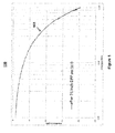
- FIG. 1 depicts the insertion loss of a conventional 31" PCB trace.
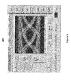
- FIG. 2 depicts an eye diagram of a data signal after passing through the 31" PCB trace of FIG. 1 .
- FIG. 3 depicts the insertion loss of a conventional 40" PCB trace.
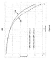
- FIG. 4 depicts the insertion loss of the 31" PCB trace of FIG. 1 and the insertion loss of the 40" PCB trace of FIG. 3 on the same graph for comparison.
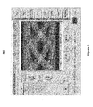
- FIG. 5 depicts an eye diagram of a data signal after passing through the 40" PCB trace of FIG. 3 .
- FIG. 6 depicts the frequency response of an emphasis filter, optimized to counteract the insertion loss of a 9" PCB trace, and the loss of a 9" PCB trace.
- FIG. 7 depicts the insertion loss of a synthesized 31" PCB trace according to an embodiment of the present invention.
- FIG. 8 depicts the insertion loss of the real 31" PCB trace of FIG. 1 and the insertion loss of the synthesized 31" PCB trace FIG. 7 on the same graph for comparison.
- FIG. 9 depicts an eye diagram of a data signal after passing through the synthesized 31" PCB trace of FIG. 7 .
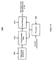
- FIG. 10 depicts a high level block diagram of a variable inter symbol interference generator according to an embodiment of the present invention.
- Embodiments of the present invention provide a variable ISI generator that generates a data signal having variable amounts of ISI by passing a data signal through (1) an emphasis or de-emphasis filter having an adjustable frequency response, and through (2) a fixed filter having a fixed frequency response such as a PCB trace, a length of cable, a discrete filter, or the like.
- FIG. 1 depicts the insertion loss (or frequency response) 105 of a conventional 31" PCB trace.
- a PCB trace is essentially a lowpass filter because it attenuates higher frequency signals. It causes fast edges of a serial digital communication signal to slow down, which closes down the region where bit decisions can be made.
- FIG. 2 depicts an eye diagram 200 of a data signal after passing through the 31" PCB trace of FIG. 1 .
- An eye diagram is a re-traced voltage-versus-time display that is triggered to re-trace on exact data bit boundaries. This shows all of the possible voltages that exist in and around a data bit when synchronized to the bit rate.
- the open area in the middle of the eye diagram represents the region where correct bit decisions can be made. It is evident from FIG. 2 that the eye opening has been compromised by adding the ISI of a 31" trace.
- FIG. 3 depicts the insertion loss 305 of a conventional 40" PCB trace. As expected, this 40" PCB trace exhibits more loss than the 31" PCB trace of FIG. 1 .
- FIG. 4 depicts the insertion loss of the traces of FIG. 1 and FIG. 3 on the same graph for comparison.
- FIG. 5 depicts an eye diagram 500 of a data signal after passing through the 40" PCB trace of FIG. 3 .
- the loss is greater for the 40" PCB trace than the 31" trace, and thus the ISI is greater as well.
- an emphasis filter is any device that conditions a data signal by adding controllable amounts of emphasis such as the BERTScope® Digital Pre-emphasis Processor DPP Series available from Tektronix, Inc. of Beaverton, Oregon.
- FIG. 6 depicts the insertion gain (or emphasis) 605 of an emphasis filter, where the parameters (also referred to as taps or coefficients) of the emphasis filter are optimized to approximate the gain needed to counteract the loss 610 of a 9" PCB trace.
- the emphasis filter is a 4-tap finite impulse response (FIR) filter with taps spaced at the bit interval, however it will be appreciated that the emphasis filter may be an infinite impulse response (IIR) filter, may use other numbers of taps or tap spacing, or may even be an analog circuit having adjustable circuit elements.
- IIR infinite impulse response
- the insertion gain of the 9" emphasis filter 605 is added to the insertion loss of the 40" PCB trace 305 to "synthesize" the frequency response of a 31" PCB trace 705 as shown in FIG. 7 .
- FIG. 8 depicts the frequency response of the synthesized 31" PCB trace 705 of FIG. 7 and the frequency response of the real 31" PCB trace 105 of FIG. 1 on the same graph for comparison.
- the synthesized frequency response 705 matches the real frequency response 105 very closely from low frequency out to several GHz. Note that very good frequency response matching at very high frequencies may not be necessary, because there is typically not much signal energy present at very high frequencies after the attenuation of cables and traces.
- FIG. 9 depicts an eye diagram 900 of a data signal after passing through the synthesized 31" PCB trace 705 of FIG. 7 . Note that the eye diagram of FIG. 9 closely approximates the eye diagram of FIG. 2 , which indicates that the performance of the synthesized 31" PCB trace closely matches the performance of the real 31" PCB trace.
- PCB traces having lengths of 32", 33", and 34" can be synthesized by concatenating a 40" PCB trace with an emphasis filter having parameters optimized to approximate the gain needed to counteract the loss of an 8", 7", and 6" PCB trace, respectively. This is a significant improvement over state-of-the-art signal generators which require manual cabling changes and/or large and expensive RF switching arrays to accomplish the same task.
- FIG. 10 depicts a variable ISI generator 1000 according to an embodiment of the present invention.
- a data signal generator 1005 produces a data signal.
- a programmable filter 1010 receives the data signal and filters it to produce an intermediate signal.
- the programmable filter 1010 is an emphasis filter that provides a programmable amount of emphasis in response to a tuning signal.
- a fixed filter 1015 having a fixed insertion loss such as a PCB trace, a length of cable, a discrete filter, or the like receives the intermediate signal and filters it to produce an output signal.
- the overall ISI stress impairment of the output signal is the concatenation of the adjustable insertion gain of the programmable filter 1010 and the fixed insertion loss of the fixed filter 1015.
- the programmable filter 1010 is an emphasis filter that provides an adjustable amount of insertion gain to improve (i.e., boost) the frequency response of the data signal, so that the combined frequency response of the programmable filter 1010 and the fixed filter 1015 provides for less ISI than the fixed filter 1015 alone.
- the programmable filter 1010 is a de-emphasis filter that provides an adjustable amount of insertion loss to degrade the frequency response of the data signal, so that the combined frequency response of the programmable filter 1010 and the fixed filter 1015 provides for more ISI than the fixed filter 1015 alone.
- an output of a data signal generator is first input to a fixed filter having a fixed insertion loss, and then input to a programmable filter to provide an equivalent result.
- a user specifies a desired amount of ISI using an input device such as a mouse, keyboard, or the like (not shown).
- the desired amount of ISI may be specified as, for example, an amount of loss in dB at a particular frequency.
- a processor 1020 programs the programmable filter 1010 so that the variable ISI generator 1000 provides a data signal having the desired amount of ISI.
- the fixed filter 1015 comprises a plurality of fixed filters and a selection circuit (not shown).
- Each of the fixed filters may be a PCB trace, a length of cable, a discrete filter, or the like.
- the selection circuit comprises one or more switches, selectors, or the like, and can be programmed to select one of the fixed filters, or a combination of the fixed filters, in order to provide a fixed insertion loss through the fixed filter 1015.
- the processor 1020 programs the selection circuit so that the fixed filter 1015 provides a portion of the desired amount of ISI (either less than or more than the desired amount of ISI), and programs the programmable filter 1010 to provide a residual amount of ISI (either insertion loss or gain), so that the combination of the programmable filter 1010 and the fixed filter 1015 provides the desired amount of ISI.
- frequency response data for each of the plurality of fixed filters is stored in a memory (not shown), and the processor 1020 programs the programmable filter 1010 based on the frequency response data associated with the selected fixed filters.
Landscapes
- Engineering & Computer Science (AREA)
- Computer Networks & Wireless Communication (AREA)
- Signal Processing (AREA)
- Quality & Reliability (AREA)
- Dc Digital Transmission (AREA)
- Filters And Equalizers (AREA)
- Digital Magnetic Recording (AREA)
- Filters That Use Time-Delay Elements (AREA)
- Noise Elimination (AREA)
Abstract
Description
- This application is a Continuation in Part of
U.S. Patent Application No. 13/219,152 U.S. Provisional Patent Application No. 61/591,595 - The present invention relates to test and measurement instruments, and more particularly to the generation of test signals with impairments.
- Many test systems need to add inter symbol interference (ISI) as a stress source when testing serial digital receivers. This is done to emulate real-life situations where long cables and/or printed circuit board (PCB) traces add ISI into a communications link. Once added, the receiver is challenged to operate in error-free conditions despite the added impairing stress. Grading mechanisms for receivers amount to seeing how much ISI a given receiver can operate error-free with. For this reason, creating a continuously variable amount of ISI in a test system is desirable.
- Continuously variable ISI has been elusive as the current state of the art employs RF switches to switch-in different lengths of PCB traces which causes a practical limitation to the number of trace length paths that can be inserted. This decreases the resolution of the varying increments of ISI. Alternatively, a large collection of fixed PCB traces can be used and manually cabled; however, this presents a problem for automatically changing between one amount of ISI stress and another.
- What is needed is a variable ISI generator.
- Embodiments of the present invention provide a variable inter symbol interference generator that generates a data signal having a variable amount of inter symbol interference by passing a data signal through (1) a programmable filter having an adjustable frequency response, and through (2) a fixed filter having a fixed frequency response such as a PCB trace, a length of cable, a discrete filter, or the like. By adjusting the parameters and therefore the insertion gain or loss of the programmable filter, and combining this with one or more fixed filters, a large range of continuously variable and finely tunable inter symbol interference amounts can be easily generated.
- The objects, advantages, and other novel features of the present invention are apparent from the following detailed description when read in conjunction with the appended claims and attached drawings.
-
FIG. 1 depicts the insertion loss of a conventional 31" PCB trace. -
FIG. 2 depicts an eye diagram of a data signal after passing through the 31" PCB trace ofFIG. 1 . -
FIG. 3 depicts the insertion loss of a conventional 40" PCB trace. -
FIG. 4 depicts the insertion loss of the 31" PCB trace ofFIG. 1 and the insertion loss of the 40" PCB trace ofFIG. 3 on the same graph for comparison. -
FIG. 5 depicts an eye diagram of a data signal after passing through the 40" PCB trace ofFIG. 3 . -
FIG. 6 depicts the frequency response of an emphasis filter, optimized to counteract the insertion loss of a 9" PCB trace, and the loss of a 9" PCB trace. -
FIG. 7 depicts the insertion loss of a synthesized 31" PCB trace according to an embodiment of the present invention. -
FIG. 8 depicts the insertion loss of the real 31" PCB trace ofFIG. 1 and the insertion loss of the synthesized 31" PCB traceFIG. 7 on the same graph for comparison. -
FIG. 9 depicts an eye diagram of a data signal after passing through the synthesized 31" PCB trace ofFIG. 7 . -
FIG. 10 depicts a high level block diagram of a variable inter symbol interference generator according to an embodiment of the present invention. - Embodiments of the present invention provide a variable ISI generator that generates a data signal having variable amounts of ISI by passing a data signal through (1) an emphasis or de-emphasis filter having an adjustable frequency response, and through (2) a fixed filter having a fixed frequency response such as a PCB trace, a length of cable, a discrete filter, or the like.
- By way of explanation, consider
FIG. 1 , which depicts the insertion loss (or frequency response) 105 of a conventional 31" PCB trace. A PCB trace is essentially a lowpass filter because it attenuates higher frequency signals. It causes fast edges of a serial digital communication signal to slow down, which closes down the region where bit decisions can be made. -
FIG. 2 depicts an eye diagram 200 of a data signal after passing through the 31" PCB trace ofFIG. 1 . An eye diagram is a re-traced voltage-versus-time display that is triggered to re-trace on exact data bit boundaries. This shows all of the possible voltages that exist in and around a data bit when synchronized to the bit rate. The open area in the middle of the eye diagram represents the region where correct bit decisions can be made. It is evident fromFIG. 2 that the eye opening has been compromised by adding the ISI of a 31" trace. -
FIG. 3 depicts theinsertion loss 305 of a conventional 40" PCB trace. As expected, this 40" PCB trace exhibits more loss than the 31" PCB trace ofFIG. 1 . -
FIG. 4 depicts the insertion loss of the traces ofFIG. 1 andFIG. 3 on the same graph for comparison. -
FIG. 5 depicts an eye diagram 500 of a data signal after passing through the 40" PCB trace ofFIG. 3 . The loss is greater for the 40" PCB trace than the 31" trace, and thus the ISI is greater as well. This causes the eye diagram ofFIG. 5 to be even more compromised than the eye diagram ofFIG. 2 . That is, the open area of the eye diagram ofFIG. 5 is smaller than the open area of the eye diagram ofFIG. 2 . - Now, an emphasis filter is any device that conditions a data signal by adding controllable amounts of emphasis such as the BERTScope® Digital Pre-emphasis Processor DPP Series available from Tektronix, Inc. of Beaverton, Oregon.
-
FIG. 6 depicts the insertion gain (or emphasis) 605 of an emphasis filter, where the parameters (also referred to as taps or coefficients) of the emphasis filter are optimized to approximate the gain needed to counteract theloss 610 of a 9" PCB trace. 9" is used in this example because 9" is the difference between the two traces shown inFIG. 4 (i.e., 40" - 31" = 9"). In this example, the emphasis filter is a 4-tap finite impulse response (FIR) filter with taps spaced at the bit interval, however it will be appreciated that the emphasis filter may be an infinite impulse response (IIR) filter, may use other numbers of taps or tap spacing, or may even be an analog circuit having adjustable circuit elements. - Now, in accordance with an embodiment of the present invention, the insertion gain of the 9" emphasis filter 605 is added to the insertion loss of the 40"
PCB trace 305 to "synthesize" the frequency response of a 31" PCB trace 705 as shown inFIG. 7 . -
FIG. 8 depicts the frequency response of the synthesized 31" PCB trace 705 ofFIG. 7 and the frequency response of the real 31" PCB trace 105 ofFIG. 1 on the same graph for comparison. The synthesizedfrequency response 705 matches thereal frequency response 105 very closely from low frequency out to several GHz. Note that very good frequency response matching at very high frequencies may not be necessary, because there is typically not much signal energy present at very high frequencies after the attenuation of cables and traces. -
FIG. 9 depicts an eye diagram 900 of a data signal after passing through the synthesized 31" PCB trace 705 ofFIG. 7 . Note that the eye diagram ofFIG. 9 closely approximates the eye diagram ofFIG. 2 , which indicates that the performance of the synthesized 31" PCB trace closely matches the performance of the real 31" PCB trace. - By adjusting the parameters and therefore the insertion gain of the emphasis filter, a large range of continuously variable and finely tunable ISI amounts can be easily generated. For example, PCB traces having lengths of 32", 33", and 34" can be synthesized by concatenating a 40" PCB trace with an emphasis filter having parameters optimized to approximate the gain needed to counteract the loss of an 8", 7", and 6" PCB trace, respectively. This is a significant improvement over state-of-the-art signal generators which require manual cabling changes and/or large and expensive RF switching arrays to accomplish the same task.
-
FIG. 10 depicts avariable ISI generator 1000 according to an embodiment of the present invention. Adata signal generator 1005 produces a data signal. Aprogrammable filter 1010 receives the data signal and filters it to produce an intermediate signal. In this embodiment, theprogrammable filter 1010 is an emphasis filter that provides a programmable amount of emphasis in response to a tuning signal. Afixed filter 1015 having a fixed insertion loss such as a PCB trace, a length of cable, a discrete filter, or the like receives the intermediate signal and filters it to produce an output signal. The overall ISI stress impairment of the output signal is the concatenation of the adjustable insertion gain of theprogrammable filter 1010 and the fixed insertion loss of thefixed filter 1015. - In the embodiment described above, the
programmable filter 1010 is an emphasis filter that provides an adjustable amount of insertion gain to improve (i.e., boost) the frequency response of the data signal, so that the combined frequency response of theprogrammable filter 1010 and the fixedfilter 1015 provides for less ISI than the fixedfilter 1015 alone. In other embodiments, theprogrammable filter 1010 is a de-emphasis filter that provides an adjustable amount of insertion loss to degrade the frequency response of the data signal, so that the combined frequency response of theprogrammable filter 1010 and the fixedfilter 1015 provides for more ISI than the fixedfilter 1015 alone. - In an alternative embodiment (not shown), an output of a data signal generator is first input to a fixed filter having a fixed insertion loss, and then input to a programmable filter to provide an equivalent result.
- Referring back to
FIG. 10 , in some embodiments, a user specifies a desired amount of ISI using an input device such as a mouse, keyboard, or the like (not shown). The desired amount of ISI may be specified as, for example, an amount of loss in dB at a particular frequency. In response, aprocessor 1020 programs theprogrammable filter 1010 so that thevariable ISI generator 1000 provides a data signal having the desired amount of ISI. - In some embodiments, the fixed
filter 1015 comprises a plurality of fixed filters and a selection circuit (not shown). Each of the fixed filters may be a PCB trace, a length of cable, a discrete filter, or the like. The selection circuit comprises one or more switches, selectors, or the like, and can be programmed to select one of the fixed filters, or a combination of the fixed filters, in order to provide a fixed insertion loss through the fixedfilter 1015. In these embodiments, theprocessor 1020 programs the selection circuit so that the fixedfilter 1015 provides a portion of the desired amount of ISI (either less than or more than the desired amount of ISI), and programs theprogrammable filter 1010 to provide a residual amount of ISI (either insertion loss or gain), so that the combination of theprogrammable filter 1010 and the fixedfilter 1015 provides the desired amount of ISI. In some embodiments, frequency response data for each of the plurality of fixed filters is stored in a memory (not shown), and theprocessor 1020 programs theprogrammable filter 1010 based on the frequency response data associated with the selected fixed filters. - It will be appreciated from the foregoing discussion that the present invention represents a significant advance in the field of test and measurement instruments. Although specific embodiments of the invention have been illustrated and described for purposes of illustration, it will be understood that various modifications may be made without departing from the spirit and scope of the invention. Accordingly, the invention should not be limited except as by the appended claims.
Claims (12)
- A variable inter symbol interference generator comprising:a data signal generator that produces a data signal;first filter means to receive and filter the data signal to produce an intermediate signal;
andsecond filter meansto receive and filter the intermediate signal to produce an output signal,wherein one of the first filter means and the second filter means comprises a fixed filter having a fixed insertion loss and the other of the first filter means and the second filter means comprises a programmable filter configured such that the output signal has a user-specified amount of inter symbol interference stress. - A variable inter symbol interference generator as in claim 1 wherein the programmable filter is an emphasis filter.
- A variable inter symbol interference generator as in claim 1 wherein the programmable filter is a de-emphasis filter.
- A variable inter symbol interference generator as in any preceding claim wherein the fixed filter comprises a plurality of fixed filters and a selection circuit that can be programmed to select one of the plurality of fixed filters, or a combination of the plurality of fixed filters, in order to provide the fixed insertion loss of the fixed filter.
- A variable inter symbol interference generator as in claim 4 further comprising a processor for programming the programmable filter and the selection circuit of the fixed filter to provide the user-specified amount of inter symbol interference stress.
- A variable inter symbol interference generator as in claim 5 wherein the processor is arranged to program the programmable filter based on frequency response data associated with the selected fixed filters.
- A method of generating a data signal having a user-specified amount of inter symbol interference comprising the steps of:producing a data signal;a first filtering step to filter the data signal to produce an intermediate signal; anda second filtering step to filter the intermediate signal to produce an output signal;wherein one of the first and second filtering steps comprises filtering with a fixed filter having a fixed insertion loss, and the other of the first and second filtering steps comprises filtering with a programmable filter such that the output signal has a user-specified amount of inter symbol interference stress.
- A method as in claim 7 wherein the programmable filter is an emphasis filter.
- A method as in claim 7 wherein the programmable filter is a de-emphasis filter.
- A method as in any of claims 7 to 9 wherein the fixed filter comprises a plurality of fixed filters and a selection circuit that can be programmed to select one of the plurality of fixed filters, or a combination of the plurality of fixed filters, in order to provide the fixed insertion loss of the fixed filter.
- A method as in claim 10 further comprising the step of programming the programmable filter and the selection circuit of the fixed filter to provide the user-specified amount of inter symbol interference stress.
- A method as in claim 11 wherein the programming step comprises the step of programming the programmable filter based on frequency response data associated with the selected fixed filters.
Applications Claiming Priority (2)
| Application Number | Priority Date | Filing Date | Title |
|---|---|---|---|
| US201261591595P | 2012-01-27 | 2012-01-27 | |
| US13/594,369 US8767870B2 (en) | 2011-02-04 | 2012-08-24 | Dynamic variable inter-symbol interference (IS) stress impairment system |
Publications (3)
| Publication Number | Publication Date |
|---|---|
| EP2621123A2 true EP2621123A2 (en) | 2013-07-31 |
| EP2621123A3 EP2621123A3 (en) | 2017-06-07 |
| EP2621123B1 EP2621123B1 (en) | 2018-12-26 |
Family
ID=47754303
Family Applications (1)
| Application Number | Title | Priority Date | Filing Date |
|---|---|---|---|
| EP13152913.3A Not-in-force EP2621123B1 (en) | 2012-01-27 | 2013-01-28 | Variable inter symbol interference generator |
Country Status (3)
| Country | Link |
|---|---|
| EP (1) | EP2621123B1 (en) |
| JP (1) | JP6292751B2 (en) |
| CN (1) | CN103227763B (en) |
Families Citing this family (2)
| Publication number | Priority date | Publication date | Assignee | Title |
|---|---|---|---|---|
| JP6571133B2 (en) * | 2017-06-19 | 2019-09-04 | アンリツ株式会社 | Signal generating apparatus and signal generating method |
| JP6625169B1 (en) * | 2018-07-27 | 2019-12-25 | アンリツ株式会社 | Signal generator and method for realizing ISI calibration channel for PCIe using the same |
Family Cites Families (14)
| Publication number | Priority date | Publication date | Assignee | Title |
|---|---|---|---|---|
| JPH0611678Y2 (en) * | 1986-03-04 | 1994-03-23 | 沖電気工業株式会社 | Automatic equalizer |
| JP3406062B2 (en) * | 1994-06-01 | 2003-05-12 | 三菱電機株式会社 | Waveform data generator |
| US7639728B2 (en) * | 2003-07-08 | 2009-12-29 | Qualcomm Incorporated | Methods for generating and transmitting frequency hopped signals |
| US7433433B2 (en) * | 2003-11-13 | 2008-10-07 | Telefonaktiebolaget L M Ericsson (Publ) | Channel estimation by adaptive interpolation |
| US7430248B2 (en) * | 2004-01-27 | 2008-09-30 | Crestcom, Inc. | Predistortion circuit and method for compensating nonlinear distortion in a digital RF communications transmitter |
| US7440497B2 (en) * | 2004-11-01 | 2008-10-21 | Lsi Corporation | Serial data link using decision feedback equalization |
| US7693691B1 (en) * | 2006-02-01 | 2010-04-06 | Altera Corporation | Systems and methods for simulating link performance |
| US8224613B2 (en) * | 2007-03-13 | 2012-07-17 | Tektronix, Inc. | Synthesis and generation of arbitrary waveforms with ISI components for jitter tolerance |
| US7852915B2 (en) * | 2007-03-21 | 2010-12-14 | Freescale Semiconductor, Inc. | Adaptive equalizer for communication channels |
| KR101131643B1 (en) * | 2007-10-03 | 2012-04-12 | 엘에스아이 코포레이션 | Continuous time-decision feedback equalizer |
| US8688400B2 (en) * | 2008-01-31 | 2014-04-01 | Tektronix International Sales Gmbh | Signal generator producing intersymbol interference effects on serial data |
| US8218611B2 (en) * | 2008-02-01 | 2012-07-10 | Tektronix International Sales Gmbh | Signal generator providing ISI scaling to touchstone files |
| JP5298894B2 (en) * | 2009-01-30 | 2013-09-25 | 富士通株式会社 | Distortion compensation device, optical receiver, and optical transmission / reception system |
| US9025652B2 (en) * | 2011-02-04 | 2015-05-05 | Tektronix, Inc. | Variable inter symbol interference generator |
-
2013
- 2013-01-25 CN CN201310027977.8A patent/CN103227763B/en not_active Expired - Fee Related
- 2013-01-28 EP EP13152913.3A patent/EP2621123B1/en not_active Not-in-force
- 2013-01-28 JP JP2013013381A patent/JP6292751B2/en not_active Expired - Fee Related
Also Published As
| Publication number | Publication date |
|---|---|
| JP2013157980A (en) | 2013-08-15 |
| CN103227763A (en) | 2013-07-31 |
| EP2621123B1 (en) | 2018-12-26 |
| JP6292751B2 (en) | 2018-03-14 |
| CN103227763B (en) | 2018-03-06 |
| EP2621123A3 (en) | 2017-06-07 |
Similar Documents
| Publication | Publication Date | Title |
|---|---|---|
| EP3285447B1 (en) | Jitter and eye contour at ber measurements after dfe | |
| US9231635B2 (en) | Apparatus and method for self-testing a component for signal recovery | |
| US8224613B2 (en) | Synthesis and generation of arbitrary waveforms with ISI components for jitter tolerance | |
| US20090119554A1 (en) | Backplane emulation technique for automated testing | |
| EP2485427B1 (en) | Variable inter symbol interference generator | |
| EP2621123B1 (en) | Variable inter symbol interference generator | |
| US8855182B2 (en) | Optimization method of optimally setting emphasis and optimization device for optimally setting emphasis | |
| US8767870B2 (en) | Dynamic variable inter-symbol interference (IS) stress impairment system | |
| US7787543B2 (en) | Pulse pattern generator and communication device evaluation system utilizing the same | |
| US9231713B2 (en) | Method for designing an analog Nyquist filter | |
| JP2018074404A (en) | Amplitude adjustment circuit, digital coherent receiver, and amplitude adjustment method | |
| JP5410454B2 (en) | PULSE PATTERN GENERATION DEVICE, ERROR RATE MEASUREMENT SYSTEM USING THE DEVICE, AND PULSE PATTERN GENERATION METHOD | |
| US20170254870A1 (en) | Methods, systems, and computer readable media for adaptively calibrating test systems for different interconnects | |
| CN120567625B (en) | Method, system and electronic device for determining configuration parameters of an equalization circuit | |
| KR100724533B1 (en) | Multichannel Processing System and its Bandpass Filtering Method | |
| Zhang et al. | A generalized structure of blind adaptive frequency-shift filter for signal extraction | |
| GB2424558A (en) | A direct determination equalizer system using cross-correlation to determine tap-coefficients | |
| Nolan | Equalization methods to improve performance of low cost copper ethernet channels | |
| Wetzker et al. | Simulation methods for time-variant wideband channels | |
| CN107735968A (en) | The apparatus and method of transmission signal | |
| KR20010008343A (en) | Apparatus for transforming signals and method thereof | |
| Wang et al. | Simulation research and parameter optimization for a frequency-domain equalizer |
Legal Events
| Date | Code | Title | Description |
|---|---|---|---|
| PUAI | Public reference made under article 153(3) epc to a published international application that has entered the european phase |
Free format text: ORIGINAL CODE: 0009012 |
|
| AK | Designated contracting states |
Kind code of ref document: A2 Designated state(s): AL AT BE BG CH CY CZ DE DK EE ES FI FR GB GR HR HU IE IS IT LI LT LU LV MC MK MT NL NO PL PT RO RS SE SI SK SM TR |
|
| AX | Request for extension of the european patent |
Extension state: BA ME |
|
| RAP1 | Party data changed (applicant data changed or rights of an application transferred) |
Owner name: TEKTRONIX, INC. |
|
| AK | Designated contracting states |
Kind code of ref document: A3 Designated state(s): AL AT BE BG CH CY CZ DE DK EE ES FI FR GB GR HR HU IE IS IT LI LT LU LV MC MK MT NL NO PL PT RO RS SE SI SK SM TR |
|
| AX | Request for extension of the european patent |
Extension state: BA ME |
|
| RIC1 | Information provided on ipc code assigned before grant |
Ipc: H04L 1/20 20060101AFI20170502BHEP Ipc: H04L 25/03 20060101ALI20170502BHEP Ipc: H04L 1/24 20060101ALI20170502BHEP Ipc: G01R 31/317 20060101ALI20170502BHEP |
|
| PUAL | Search report despatched |
Free format text: ORIGINAL CODE: 0009013 |
|
| STAA | Information on the status of an ep patent application or granted ep patent |
Free format text: STATUS: REQUEST FOR EXAMINATION WAS MADE |
|
| 17P | Request for examination filed |
Effective date: 20171206 |
|
| RBV | Designated contracting states (corrected) |
Designated state(s): AL AT BE BG CH CY CZ DE DK EE ES FI FR GB GR HR HU IE IS IT LI LT LU LV MC MK MT NL NO PL PT RO RS SE SI SK SM TR |
|
| GRAP | Despatch of communication of intention to grant a patent |
Free format text: ORIGINAL CODE: EPIDOSNIGR1 |
|
| STAA | Information on the status of an ep patent application or granted ep patent |
Free format text: STATUS: GRANT OF PATENT IS INTENDED |
|
| INTG | Intention to grant announced |
Effective date: 20180706 |
|
| GRAS | Grant fee paid |
Free format text: ORIGINAL CODE: EPIDOSNIGR3 |
|
| GRAA | (expected) grant |
Free format text: ORIGINAL CODE: 0009210 |
|
| STAA | Information on the status of an ep patent application or granted ep patent |
Free format text: STATUS: THE PATENT HAS BEEN GRANTED |
|
| AK | Designated contracting states |
Kind code of ref document: B1 Designated state(s): AL AT BE BG CH CY CZ DE DK EE ES FI FR GB GR HR HU IE IS IT LI LT LU LV MC MK MT NL NO PL PT RO RS SE SI SK SM TR |
|
| REG | Reference to a national code |
Ref country code: GB Ref legal event code: FG4D |
|
| REG | Reference to a national code |
Ref country code: CH Ref legal event code: EP |
|
| REG | Reference to a national code |
Ref country code: AT Ref legal event code: REF Ref document number: 1082887 Country of ref document: AT Kind code of ref document: T Effective date: 20190115 |
|
| REG | Reference to a national code |
Ref country code: DE Ref legal event code: R096 Ref document number: 602013048639 Country of ref document: DE |
|
| REG | Reference to a national code |
Ref country code: IE Ref legal event code: FG4D |
|
| PG25 | Lapsed in a contracting state [announced via postgrant information from national office to epo] |
Ref country code: LV Free format text: LAPSE BECAUSE OF FAILURE TO SUBMIT A TRANSLATION OF THE DESCRIPTION OR TO PAY THE FEE WITHIN THE PRESCRIBED TIME-LIMIT Effective date: 20181226 Ref country code: FI Free format text: LAPSE BECAUSE OF FAILURE TO SUBMIT A TRANSLATION OF THE DESCRIPTION OR TO PAY THE FEE WITHIN THE PRESCRIBED TIME-LIMIT Effective date: 20181226 Ref country code: HR Free format text: LAPSE BECAUSE OF FAILURE TO SUBMIT A TRANSLATION OF THE DESCRIPTION OR TO PAY THE FEE WITHIN THE PRESCRIBED TIME-LIMIT Effective date: 20181226 Ref country code: NO Free format text: LAPSE BECAUSE OF FAILURE TO SUBMIT A TRANSLATION OF THE DESCRIPTION OR TO PAY THE FEE WITHIN THE PRESCRIBED TIME-LIMIT Effective date: 20190326 Ref country code: BG Free format text: LAPSE BECAUSE OF FAILURE TO SUBMIT A TRANSLATION OF THE DESCRIPTION OR TO PAY THE FEE WITHIN THE PRESCRIBED TIME-LIMIT Effective date: 20190326 Ref country code: LT Free format text: LAPSE BECAUSE OF FAILURE TO SUBMIT A TRANSLATION OF THE DESCRIPTION OR TO PAY THE FEE WITHIN THE PRESCRIBED TIME-LIMIT Effective date: 20181226 |
|
| PGFP | Annual fee paid to national office [announced via postgrant information from national office to epo] |
Ref country code: GB Payment date: 20190205 Year of fee payment: 7 Ref country code: DE Payment date: 20190208 Year of fee payment: 7 |
|
| REG | Reference to a national code |
Ref country code: NL Ref legal event code: MP Effective date: 20181226 |
|
| REG | Reference to a national code |
Ref country code: LT Ref legal event code: MG4D |
|
| PG25 | Lapsed in a contracting state [announced via postgrant information from national office to epo] |
Ref country code: RS Free format text: LAPSE BECAUSE OF FAILURE TO SUBMIT A TRANSLATION OF THE DESCRIPTION OR TO PAY THE FEE WITHIN THE PRESCRIBED TIME-LIMIT Effective date: 20181226 Ref country code: GR Free format text: LAPSE BECAUSE OF FAILURE TO SUBMIT A TRANSLATION OF THE DESCRIPTION OR TO PAY THE FEE WITHIN THE PRESCRIBED TIME-LIMIT Effective date: 20190327 Ref country code: AL Free format text: LAPSE BECAUSE OF FAILURE TO SUBMIT A TRANSLATION OF THE DESCRIPTION OR TO PAY THE FEE WITHIN THE PRESCRIBED TIME-LIMIT Effective date: 20181226 Ref country code: SE Free format text: LAPSE BECAUSE OF FAILURE TO SUBMIT A TRANSLATION OF THE DESCRIPTION OR TO PAY THE FEE WITHIN THE PRESCRIBED TIME-LIMIT Effective date: 20181226 |
|
| REG | Reference to a national code |
Ref country code: AT Ref legal event code: MK05 Ref document number: 1082887 Country of ref document: AT Kind code of ref document: T Effective date: 20181226 |
|
| PG25 | Lapsed in a contracting state [announced via postgrant information from national office to epo] |
Ref country code: NL Free format text: LAPSE BECAUSE OF FAILURE TO SUBMIT A TRANSLATION OF THE DESCRIPTION OR TO PAY THE FEE WITHIN THE PRESCRIBED TIME-LIMIT Effective date: 20181226 |
|
| PG25 | Lapsed in a contracting state [announced via postgrant information from national office to epo] |
Ref country code: PL Free format text: LAPSE BECAUSE OF FAILURE TO SUBMIT A TRANSLATION OF THE DESCRIPTION OR TO PAY THE FEE WITHIN THE PRESCRIBED TIME-LIMIT Effective date: 20181226 Ref country code: PT Free format text: LAPSE BECAUSE OF FAILURE TO SUBMIT A TRANSLATION OF THE DESCRIPTION OR TO PAY THE FEE WITHIN THE PRESCRIBED TIME-LIMIT Effective date: 20190426 Ref country code: CZ Free format text: LAPSE BECAUSE OF FAILURE TO SUBMIT A TRANSLATION OF THE DESCRIPTION OR TO PAY THE FEE WITHIN THE PRESCRIBED TIME-LIMIT Effective date: 20181226 Ref country code: ES Free format text: LAPSE BECAUSE OF FAILURE TO SUBMIT A TRANSLATION OF THE DESCRIPTION OR TO PAY THE FEE WITHIN THE PRESCRIBED TIME-LIMIT Effective date: 20181226 Ref country code: IT Free format text: LAPSE BECAUSE OF FAILURE TO SUBMIT A TRANSLATION OF THE DESCRIPTION OR TO PAY THE FEE WITHIN THE PRESCRIBED TIME-LIMIT Effective date: 20181226 |
|
| PG25 | Lapsed in a contracting state [announced via postgrant information from national office to epo] |
Ref country code: RO Free format text: LAPSE BECAUSE OF FAILURE TO SUBMIT A TRANSLATION OF THE DESCRIPTION OR TO PAY THE FEE WITHIN THE PRESCRIBED TIME-LIMIT Effective date: 20181226 Ref country code: IS Free format text: LAPSE BECAUSE OF FAILURE TO SUBMIT A TRANSLATION OF THE DESCRIPTION OR TO PAY THE FEE WITHIN THE PRESCRIBED TIME-LIMIT Effective date: 20190426 Ref country code: SK Free format text: LAPSE BECAUSE OF FAILURE TO SUBMIT A TRANSLATION OF THE DESCRIPTION OR TO PAY THE FEE WITHIN THE PRESCRIBED TIME-LIMIT Effective date: 20181226 Ref country code: EE Free format text: LAPSE BECAUSE OF FAILURE TO SUBMIT A TRANSLATION OF THE DESCRIPTION OR TO PAY THE FEE WITHIN THE PRESCRIBED TIME-LIMIT Effective date: 20181226 Ref country code: SM Free format text: LAPSE BECAUSE OF FAILURE TO SUBMIT A TRANSLATION OF THE DESCRIPTION OR TO PAY THE FEE WITHIN THE PRESCRIBED TIME-LIMIT Effective date: 20181226 |
|
| REG | Reference to a national code |
Ref country code: CH Ref legal event code: PL |
|
| REG | Reference to a national code |
Ref country code: DE Ref legal event code: R097 Ref document number: 602013048639 Country of ref document: DE |
|
| PG25 | Lapsed in a contracting state [announced via postgrant information from national office to epo] |
Ref country code: LU Free format text: LAPSE BECAUSE OF NON-PAYMENT OF DUE FEES Effective date: 20190128 |
|
| REG | Reference to a national code |
Ref country code: BE Ref legal event code: MM Effective date: 20190131 |
|
| REG | Reference to a national code |
Ref country code: IE Ref legal event code: MM4A |
|
| PG25 | Lapsed in a contracting state [announced via postgrant information from national office to epo] |
Ref country code: MC Free format text: LAPSE BECAUSE OF FAILURE TO SUBMIT A TRANSLATION OF THE DESCRIPTION OR TO PAY THE FEE WITHIN THE PRESCRIBED TIME-LIMIT Effective date: 20181226 Ref country code: DK Free format text: LAPSE BECAUSE OF FAILURE TO SUBMIT A TRANSLATION OF THE DESCRIPTION OR TO PAY THE FEE WITHIN THE PRESCRIBED TIME-LIMIT Effective date: 20181226 Ref country code: AT Free format text: LAPSE BECAUSE OF FAILURE TO SUBMIT A TRANSLATION OF THE DESCRIPTION OR TO PAY THE FEE WITHIN THE PRESCRIBED TIME-LIMIT Effective date: 20181226 |
|
| PLBE | No opposition filed within time limit |
Free format text: ORIGINAL CODE: 0009261 |
|
| STAA | Information on the status of an ep patent application or granted ep patent |
Free format text: STATUS: NO OPPOSITION FILED WITHIN TIME LIMIT |
|
| PG25 | Lapsed in a contracting state [announced via postgrant information from national office to epo] |
Ref country code: BE Free format text: LAPSE BECAUSE OF NON-PAYMENT OF DUE FEES Effective date: 20190131 |
|
| 26N | No opposition filed |
Effective date: 20190927 |
|
| PG25 | Lapsed in a contracting state [announced via postgrant information from national office to epo] |
Ref country code: LI Free format text: LAPSE BECAUSE OF NON-PAYMENT OF DUE FEES Effective date: 20190131 Ref country code: CH Free format text: LAPSE BECAUSE OF NON-PAYMENT OF DUE FEES Effective date: 20190131 |
|
| PG25 | Lapsed in a contracting state [announced via postgrant information from national office to epo] |
Ref country code: IE Free format text: LAPSE BECAUSE OF NON-PAYMENT OF DUE FEES Effective date: 20190128 |
|
| PG25 | Lapsed in a contracting state [announced via postgrant information from national office to epo] |
Ref country code: SI Free format text: LAPSE BECAUSE OF FAILURE TO SUBMIT A TRANSLATION OF THE DESCRIPTION OR TO PAY THE FEE WITHIN THE PRESCRIBED TIME-LIMIT Effective date: 20181226 Ref country code: FR Free format text: LAPSE BECAUSE OF NON-PAYMENT OF DUE FEES Effective date: 20190226 |
|
| PG25 | Lapsed in a contracting state [announced via postgrant information from national office to epo] |
Ref country code: TR Free format text: LAPSE BECAUSE OF FAILURE TO SUBMIT A TRANSLATION OF THE DESCRIPTION OR TO PAY THE FEE WITHIN THE PRESCRIBED TIME-LIMIT Effective date: 20181226 |
|
| PG25 | Lapsed in a contracting state [announced via postgrant information from national office to epo] |
Ref country code: MT Free format text: LAPSE BECAUSE OF NON-PAYMENT OF DUE FEES Effective date: 20190128 |
|
| REG | Reference to a national code |
Ref country code: DE Ref legal event code: R119 Ref document number: 602013048639 Country of ref document: DE |
|
| GBPC | Gb: european patent ceased through non-payment of renewal fee |
Effective date: 20200128 |
|
| PG25 | Lapsed in a contracting state [announced via postgrant information from national office to epo] |
Ref country code: DE Free format text: LAPSE BECAUSE OF NON-PAYMENT OF DUE FEES Effective date: 20200801 Ref country code: GB Free format text: LAPSE BECAUSE OF NON-PAYMENT OF DUE FEES Effective date: 20200128 |
|
| PG25 | Lapsed in a contracting state [announced via postgrant information from national office to epo] |
Ref country code: CY Free format text: LAPSE BECAUSE OF FAILURE TO SUBMIT A TRANSLATION OF THE DESCRIPTION OR TO PAY THE FEE WITHIN THE PRESCRIBED TIME-LIMIT Effective date: 20181226 |
|
| PG25 | Lapsed in a contracting state [announced via postgrant information from national office to epo] |
Ref country code: HU Free format text: LAPSE BECAUSE OF FAILURE TO SUBMIT A TRANSLATION OF THE DESCRIPTION OR TO PAY THE FEE WITHIN THE PRESCRIBED TIME-LIMIT; INVALID AB INITIO Effective date: 20130128 |
|
| PG25 | Lapsed in a contracting state [announced via postgrant information from national office to epo] |
Ref country code: MK Free format text: LAPSE BECAUSE OF FAILURE TO SUBMIT A TRANSLATION OF THE DESCRIPTION OR TO PAY THE FEE WITHIN THE PRESCRIBED TIME-LIMIT Effective date: 20181226 |