EP2620979A2 - Encapsulant with corosion inhibitor - Google Patents
Encapsulant with corosion inhibitor Download PDFInfo
- Publication number
- EP2620979A2 EP2620979A2 EP13151813.6A EP13151813A EP2620979A2 EP 2620979 A2 EP2620979 A2 EP 2620979A2 EP 13151813 A EP13151813 A EP 13151813A EP 2620979 A2 EP2620979 A2 EP 2620979A2
- Authority
- EP
- European Patent Office
- Prior art keywords
- electronic device
- encapsulant
- negatively
- corrosion inhibitor
- charged
- Prior art date
- Legal status (The legal status is an assumption and is not a legal conclusion. Google has not performed a legal analysis and makes no representation as to the accuracy of the status listed.)
- Withdrawn
Links
Images


Classifications
-
- H—ELECTRICITY
- H10—SEMICONDUCTOR DEVICES; ELECTRIC SOLID-STATE DEVICES NOT OTHERWISE PROVIDED FOR
- H10W—GENERIC PACKAGES, INTERCONNECTIONS, CONNECTORS OR OTHER CONSTRUCTIONAL DETAILS OF DEVICES COVERED BY CLASS H10
- H10W74/00—Encapsulations, e.g. protective coatings
- H10W74/40—Encapsulations, e.g. protective coatings characterised by their materials
- H10W74/47—Encapsulations, e.g. protective coatings characterised by their materials comprising organic materials, e.g. plastics or resins
-
- H—ELECTRICITY
- H10—SEMICONDUCTOR DEVICES; ELECTRIC SOLID-STATE DEVICES NOT OTHERWISE PROVIDED FOR
- H10W—GENERIC PACKAGES, INTERCONNECTIONS, CONNECTORS OR OTHER CONSTRUCTIONAL DETAILS OF DEVICES COVERED BY CLASS H10
- H10W72/00—Interconnections or connectors in packages
- H10W72/50—Bond wires
- H10W72/531—Shapes of wire connectors
- H10W72/536—Shapes of wire connectors the connected ends being ball-shaped
-
- H—ELECTRICITY
- H10—SEMICONDUCTOR DEVICES; ELECTRIC SOLID-STATE DEVICES NOT OTHERWISE PROVIDED FOR
- H10W—GENERIC PACKAGES, INTERCONNECTIONS, CONNECTORS OR OTHER CONSTRUCTIONAL DETAILS OF DEVICES COVERED BY CLASS H10
- H10W72/00—Interconnections or connectors in packages
- H10W72/50—Bond wires
- H10W72/551—Materials of bond wires
- H10W72/552—Materials of bond wires comprising metals or metalloids, e.g. silver
- H10W72/5524—Materials of bond wires comprising metals or metalloids, e.g. silver comprising aluminium [Al]
-
- H—ELECTRICITY
- H10—SEMICONDUCTOR DEVICES; ELECTRIC SOLID-STATE DEVICES NOT OTHERWISE PROVIDED FOR
- H10W—GENERIC PACKAGES, INTERCONNECTIONS, CONNECTORS OR OTHER CONSTRUCTIONAL DETAILS OF DEVICES COVERED BY CLASS H10
- H10W72/00—Interconnections or connectors in packages
- H10W72/50—Bond wires
- H10W72/59—Bond pads specially adapted therefor
-
- H—ELECTRICITY
- H10—SEMICONDUCTOR DEVICES; ELECTRIC SOLID-STATE DEVICES NOT OTHERWISE PROVIDED FOR
- H10W—GENERIC PACKAGES, INTERCONNECTIONS, CONNECTORS OR OTHER CONSTRUCTIONAL DETAILS OF DEVICES COVERED BY CLASS H10
- H10W72/00—Interconnections or connectors in packages
- H10W72/90—Bond pads, in general
- H10W72/931—Shapes of bond pads
- H10W72/934—Cross-sectional shape, i.e. in side view
-
- H—ELECTRICITY
- H10—SEMICONDUCTOR DEVICES; ELECTRIC SOLID-STATE DEVICES NOT OTHERWISE PROVIDED FOR
- H10W—GENERIC PACKAGES, INTERCONNECTIONS, CONNECTORS OR OTHER CONSTRUCTIONAL DETAILS OF DEVICES COVERED BY CLASS H10
- H10W72/00—Interconnections or connectors in packages
- H10W72/90—Bond pads, in general
- H10W72/981—Auxiliary members, e.g. spacers
- H10W72/983—Reinforcing structures, e.g. collars
-
- H—ELECTRICITY
- H10—SEMICONDUCTOR DEVICES; ELECTRIC SOLID-STATE DEVICES NOT OTHERWISE PROVIDED FOR
- H10W—GENERIC PACKAGES, INTERCONNECTIONS, CONNECTORS OR OTHER CONSTRUCTIONAL DETAILS OF DEVICES COVERED BY CLASS H10
- H10W74/00—Encapsulations, e.g. protective coatings
Definitions
- This invention relates to packaged electronic devices.
- Electronic devices such as semiconductor devices can be encapsulated in an encapsulant such as a mold compound.
- an encapsulant such as a mold compound.
- corrosive substances such as chloride ions in presence of moisture in the encapsulant can attack certain metals that are susceptible to corrosion.
- One way to reduce the corrosion is to reduce the amount of the corrosive substance in the encapsulant such as reducing the amount of chloride.
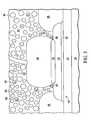
- Figure 3 shows a portion of the packaged electronic device of Figure 2 according to one embodiment of the present invention.
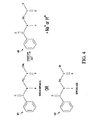
- Figure 4 shows models of corrosion inhibitor ions according to two embodiments of the present invention.
- including negatively charged corrosion inhibitors in an encapsulant for a packaged electronic device may inhibit corrosion in wire bond pads of the electronic device.
- the negatively charged corrosion inhibitors are attracted to positively charged structures of the electronic device wherein the attracted corrosion inhibitors prevent other corrosive substances from causing corrosion of susceptible surfaces of the positively charge structures.
- Figure 1 is a partial cutaway cross-section of an electronic device where wires are wire bonded to conductive bond pads.
- electronic device is an integrated circuit 101 that includes multiple transistors (e.g. 105) and/or other types of semiconductor devices (e.g. diodes (not shown)) implemented in a semiconductor material (e.g. semiconductor substrate 103).
- transistor 105 is a CMOS transistor implemented in silicon substrate 103.
- an integrated circuit may include other types semiconductor devices and/or have other configurations.
- the semiconductor devices of integrated circuit 101 are electrically coupled together by conductive interconnect structures located in one or more interconnect layers (107, 111, and 113).
- the conductive interconnect structures (e.g. 109, 117, and 121) of the interconnect layers are coupled to other conductive interconnect structures of other interconnect layers with conductive vias (e.g. 115, 119) or conductive plugs.
- the conductive interconnect structures and vias are made of a conductive material (e.g. copper, gold, aluminum, titanium).
- the conductive interconnect structures may include diffusions layers and barrier layers.
- the conductive structures are located in interlayer dielectric material 120 (e.g. an oxide formed by a TEOS process or other types of dielectric materials) to isolate the electrically conductive structures.
- the conductive interconnect layers and dielectric material are sequentially formed in layers over substrate 103 from the bottom of the page to the top of the page.
- wire bond pads 121 and 123 are formed on interconnects structures (e.g. 121) of the final interconnect layer 113.
- interconnects of the final interconnect layer 113 are made of copper
- a diffusion barrier 125 e.g. tantalum
- an aluminum bond pad layer 127 is formed on the diffusion barrier 125.
- a passivation layer 135 of a dielectric material is formed over integrated circuit 101 to electrically isolate and protect integrated circuit 101. Openings are made in passivation layer 135 to expose the bond pad layers (e.g. 127).
- passivation layer 135 the wafer on which integrated circuit 101 is formed is then singulated into multiple integrated circuits. Those integrated circuits maybe mounted on structures such as substrates or lead frames.
- wires (131) are attached by a wire bonding process to bond pads (121, 123) with a wire bonding material (e.g. ball bond 129).
- Wire 131 and bonding material (ball bond 129) form a wire bond.
- the other end of the wires 131 are attached to a conductive structure of the substrates or lead frame (not shown) with e.g. a stitch bond.
- wire 131 is attached to a bond pad of integrated circuit 101 with a ball bonding wire bond process
- wires 131 may be attached to a bond pad by other wire bonding techniques e.g. such as stitch bonding or wedge bonding.
- a multiphase material layer 133 of intermetalic compounds of aluminum and copper form at the interface of layer 127 and bonding material of ball bond 129, as a result of wire bonding or subsequent thermal process such as e.g. a die attach curing process or testing process.
- This multiphase material layer 133 may be susceptible to corrosion from corrosive substances in a subsequently formed encapsulant.
- the material of layer 133 may be "copper rich" at the top and aluminum rich at the bottom of layer 133.
- corrosion inhibitors and/or diffusion barrier layers of other material such as e.g. a stack layer of Nickel/Palladium/Gold may be applied to layer 127 prior to wire bonding.
- ball bond 129 and layer 127 each may be made of other materials (e.g. copper, aluminum, gold, metal alloys) in other embodiments.
- Figure 2 shows a portion of packaged electronic device 200 after integrated circuit 101, wires 131, and the substrate or leadframe (not shown) are encapsulated with an encapsulant 201.
- encapsulant 201 is applied to the integrated circuit by a transfer molding process, but may be applied by other encapsulating processes e.g. such as a center gate molding process or injection molding process in other embodiments.
- the encapsulated packages may be encapsulated in panels and then separated into the individual packages.
- encapsulant 201 is made of molding compound.
- the molding compound includes silica fillers (70-80% by volume), an epoxy resin (10-20% by volume), hardeners (5-10% by volume), and flame retardants (1-4% by volume).
- Encapsulant 201 may also include materials such as stress release agents, catalyst accelerators, carbon black, release agents, and coloring agents.
- an encapsulant may include different materials, a different combination of materials, and/or have a different percentage of materials.
- Figure 3 is a more detailed view of pad 123 that is shown in Figure 2 .
- individual particles located in the encapsulant 201 are shown for illustrative purposes and are not drawn to scale.
- Figure 3 shows silica particles 301 distributed throughout encapsulant 201.
- chloride ions 303 are also shown distributed in encapsulant 201. These chloride ions (Cl - ) may be generated from the different components of the encapsulant. Mold compounds absorb moisture (e.g. moisture content 0.1 - 0.5 %) that with ionic impurities such as chloride can form electrolytes capable of causing corrosion to structures involving metals. Susceptibility of corrosion for metals vary from metal to metal and governed by thermodynamic and kinetic principles. For example, chloride ions 303 may cause corrosion in multiphase material layer 133 in that layer 133 is susceptible to corrosion.
- some bond pads may be biased at a positive voltage (e.g. 2.2 V, 4 V, or 5 V), such as bond pads that are designed to supply integrated circuit 101 with a positive supply voltage (VDD).
- a positive voltage e.g. 2.2 V, 4 V, or 5 V
- conductive structures that are adjacent to the encapsulant attract and cause to migrate the negative charged ions such as chloride ions 303 towards such positively based structures or pins.
- the buildup of the chloride ions at the positively charged conductive structures can cause corrosion of the materials that are susceptible to corrosion. For example, chloride ions that are attracted to a positively charged bond pad 123 and material of ball bond 129, may cause corrosion of multiphase material layer 133. Such corrosion may lead to an increased resistance or to a complete open of the bond pad/wire bond connection of a positively charged bond pad.
- encapsulant 201 is formed to include negatively charged corrosion inhibitors.
- the corrosion inhibitors are particles labeled "I - ".
- these corrosion inhibitors (305, 307, 309) are negatively charged ions or capable of forming charged ions that are attracted to positively charged structures of the bond pad and wire bond.
- the corrosion inhibitor ions migrate towards the positively charged structures and are believed to be adsorbed to active sites on the surfaces that have a potential for corrosion.
- the adsorption of the negatively charge corrosion inhibitor ions (307, 309) on such surfaces inhibits the corrosion caused by chloride ions on those surfaces.
- the number of inhibitor ions is greater than the number of chloride ions such that an inhibitor ion is more likely to be absorbed to a positively charged structure than a chloride ion.
- the number of inhibitor ions in the encapsulant is at least twice as many as the number of chloride ions. In some embodiments, higher ratios of inhibitor ions to chloride ions is preferable (e.g. 5 or greater inhibitor ions to 1 chloride ion or greater) in that it provides a greater number of inhibitor ions to be adsorbed to the susceptible structures.
- the number of negatively charged inhibitor ions is 150 parts per million (ppm) or greater. In other embodiments, number of inhibitor ions may be around 200 ppm.
- the concentration of inhibitor ions added to an encapsulant is dependent on the number of chloride ions in the encapsulant.
- FIG. 4 shows two embodiments of the formation of corrosion inhibitors from an ionization process.
- Molecular diagram 401 represents a molecule of sodium hippurate.
- Molecular diagram 403 represents a molecule of hippuric acid.
- either one of the substances may be added to an encapsulant before the encapsulating process. In the presence of moisture and appropriate pH conditions, these molecules ionize to form negatively charged hippurate ions 407, which act as corrosion inhibitors in the encapsulant.
- other soluble salts e.g. potassium or ammonium hippurate
- the potassium hippurate or ammonium hippurate ionizes to form negatively charged hippurate ions which act as a corrosion inhibitor.
- HEDP 1-Hydroxyethylidene-1,1-Diphosphonic Acid
- HEDP 1-Hydroxyethylidene-1,1-Diphosphonic Acid
- Other types of inhibitors that may be used include negative ions of organic acids such as acetates, formates, and tartarates and negative ions of inorganic acids such as phosphates, silicates and nitrites.
- salts which can form the negatively charged ions may be added directly to the encapsulant prior to encapsulation. These substances can also be added as mixtures.
- an encapsulant may include multiple types of corrosion inhibitors, such as anions of both organic and inorganic acids.
- Adding negatively charge corrosion inhibitors to the encapsulant may inhibit the corrosive effect of chloride ions on conductive structures such as on intermetallic compounds formed between bonding metals such as copper and Al which can positively charged during the operation and/or testing of the packaged device.
- the corrosion inhibitors are adsorbed to the susceptible surfaces to prevent negatively charged ions from attacking those surfaces.
- the substances that form the negatively charged ion inhibitors may be applied to the bond pads prior to wire bonding.
- packages electronic devices may include other types of electronic devices (e.g. capacitors, inductors) in other embodiments.
- a packaged electronic device may include multiple electronic devices coupled together.
- an encapsulated integrated circuit may have other configurations/structures in other embodiments, e.g. such as underfill encapsulating materials used in flip chip applications.
- a packaged electronic device includes an electronic device, a conductive structure, an encapsulant encapsulating the conductive structure.
- the encapsulant includes chlorides and a negatively-charged corrosion inhibitor.
- a method of making a packaged electronic device includes providing an electronic device and a conductive structure electrically coupled to the electronic device and applying an encapsulant to the conductive structure.
- the encapsulant includes chlorides and a negatively-charged corrosion inhibitor.
- a packaged electronic device in another embodiment, includes an electronic device including a bond pad having an upper surface comprising aluminum, a wire bond including a copper ball bond attached to the bond pad so as to have an intermetallic layer of copper and aluminum between the bond pad and the wire bond, the wire bond including a wire, and an encapsulant encapsulating the wire bond.
- the encapsulant includes chlorides and a negatively-charged corrosion inhibitor.
Landscapes
- Wire Bonding (AREA)
- Prevention Of Electric Corrosion (AREA)
- Preventing Corrosion Or Incrustation Of Metals (AREA)
Abstract
A packaged electronic device including an electronic device (101), a conductive structure (129), and an encapsulant (201). The encapsulant has chlorides (303) and a negatively-charged corrosion inhibitor (307) for preventing corrosion of the conductive structure.
Description
- This invention relates to packaged electronic devices.
- Electronic devices such as semiconductor devices can be encapsulated in an encapsulant such as a mold compound. One problem with such packaged electronic devices is that corrosive substances such as chloride ions in presence of moisture in the encapsulant can attack certain metals that are susceptible to corrosion. One way to reduce the corrosion is to reduce the amount of the corrosive substance in the encapsulant such as reducing the amount of chloride.
- The present invention may be better understood, and its numerous objects, features, and advantages made apparent to those skilled in the art by referencing the accompanying drawings.
-
Figures 1 and2 set forth partial cut away side views of a packaged electronic device in various stages of its manufacture according to one embodiment of the present invention. -
Figure 3 shows a portion of the packaged electronic device ofFigure 2 according to one embodiment of the present invention. -
Figure 4 shows models of corrosion inhibitor ions according to two embodiments of the present invention. - The use of the same reference symbols in different drawings indicates identical items unless otherwise noted. The Figures are not necessarily drawn to scale.
- The following sets forth a detailed description of a mode for carrying out the invention. The description is intended to be illustrative of the invention and should not be taken to be limiting.
- It has been discovered that including negatively charged corrosion inhibitors in an encapsulant for a packaged electronic device may inhibit corrosion in wire bond pads of the electronic device. In one example, the negatively charged corrosion inhibitors are attracted to positively charged structures of the electronic device wherein the attracted corrosion inhibitors prevent other corrosive substances from causing corrosion of susceptible surfaces of the positively charge structures.
-
Figure 1 is a partial cutaway cross-section of an electronic device where wires are wire bonded to conductive bond pads. In the embodiment ofFigure 1 , electronic device is an integratedcircuit 101 that includes multiple transistors (e.g. 105) and/or other types of semiconductor devices (e.g. diodes (not shown)) implemented in a semiconductor material (e.g. semiconductor substrate 103). In one example,transistor 105 is a CMOS transistor implemented insilicon substrate 103. However, in other embodiments, an integrated circuit may include other types semiconductor devices and/or have other configurations. - In the embodiment shown, the semiconductor devices of integrated
circuit 101 are electrically coupled together by conductive interconnect structures located in one or more interconnect layers (107, 111, and 113). The conductive interconnect structures (e.g. 109, 117, and 121) of the interconnect layers are coupled to other conductive interconnect structures of other interconnect layers with conductive vias (e.g. 115, 119) or conductive plugs. The conductive interconnect structures and vias are made of a conductive material (e.g. copper, gold, aluminum, titanium). The conductive interconnect structures may include diffusions layers and barrier layers. The conductive structures are located in interlayer dielectric material 120 (e.g. an oxide formed by a TEOS process or other types of dielectric materials) to isolate the electrically conductive structures. In one embodiment, the conductive interconnect layers and dielectric material are sequentially formed in layers oversubstrate 103 from the bottom of the page to the top of the page. - In the embodiment shown,
wire bond pads final interconnect layer 113. In one embodiment where interconnects of thefinal interconnect layer 113 are made of copper, a diffusion barrier 125 (e.g. tantalum) is formed on the copper wherein an aluminumbond pad layer 127 is formed on thediffusion barrier 125. Afterwards, apassivation layer 135 of a dielectric material is formed over integratedcircuit 101 to electrically isolate and protect integratedcircuit 101. Openings are made inpassivation layer 135 to expose the bond pad layers (e.g. 127). - After the formation of
passivation layer 135, the wafer on which integratedcircuit 101 is formed is then singulated into multiple integrated circuits. Those integrated circuits maybe mounted on structures such as substrates or lead frames. - After the integrated circuit is mounted to a substrate or lead frame, wires (131) are attached by a wire bonding process to bond pads (121, 123) with a wire bonding material (e.g. ball bond 129).
Wire 131 and bonding material (ball bond 129) form a wire bond. The other end of thewires 131 are attached to a conductive structure of the substrates or lead frame (not shown) with e.g. a stitch bond. Although in the embodiment shown,wire 131 is attached to a bond pad of integratedcircuit 101 with a ball bonding wire bond process,wires 131 may be attached to a bond pad by other wire bonding techniques e.g. such as stitch bonding or wedge bonding. - In one embodiment where the conductive ball bonding material of
ball bond 129 is copper (e.g. is greater than 95% copper) andpad layer 127 is aluminum (e.g. greater than 95% aluminum), amultiphase material layer 133 of intermetalic compounds of aluminum and copper form at the interface oflayer 127 and bonding material ofball bond 129, as a result of wire bonding or subsequent thermal process such as e.g. a die attach curing process or testing process. Thismultiphase material layer 133 may be susceptible to corrosion from corrosive substances in a subsequently formed encapsulant. In some embodiments, the material oflayer 133 may be "copper rich" at the top and aluminum rich at the bottom oflayer 133. In some embodiments, corrosion inhibitors and/or diffusion barrier layers of other material such as e.g. a stack layer of Nickel/Palladium/Gold may be applied tolayer 127 prior to wire bonding. In other embodiments,ball bond 129 andlayer 127 each may be made of other materials (e.g. copper, aluminum, gold, metal alloys) in other embodiments. -
Figure 2 shows a portion of packagedelectronic device 200 after integratedcircuit 101,wires 131, and the substrate or leadframe (not shown) are encapsulated with anencapsulant 201. In one embodiment,encapsulant 201 is applied to the integrated circuit by a transfer molding process, but may be applied by other encapsulating processes e.g. such as a center gate molding process or injection molding process in other embodiments. In some embodiments, the encapsulated packages may be encapsulated in panels and then separated into the individual packages. - In one embodiment,
encapsulant 201 is made of molding compound. In one example, the molding compound includes silica fillers (70-80% by volume), an epoxy resin (10-20% by volume), hardeners (5-10% by volume), and flame retardants (1-4% by volume). Encapsulant 201 may also include materials such as stress release agents, catalyst accelerators, carbon black, release agents, and coloring agents. However, in other embodiments, an encapsulant may include different materials, a different combination of materials, and/or have a different percentage of materials. -
Figure 3 is a more detailed view ofpad 123 that is shown inFigure 2 . In the view ofFigure 3 , individual particles located in theencapsulant 201 are shown for illustrative purposes and are not drawn to scale.Figure 3 showssilica particles 301 distributed throughoutencapsulant 201. - Also shown distributed in
encapsulant 201 are negatively chargedchloride ions 303. These chloride ions (Cl-) may be generated from the different components of the encapsulant. Mold compounds absorb moisture (e.g. moisture content 0.1 - 0.5 %) that with ionic impurities such as chloride can form electrolytes capable of causing corrosion to structures involving metals. Susceptibility of corrosion for metals vary from metal to metal and governed by thermodynamic and kinetic principles. For example,chloride ions 303 may cause corrosion inmultiphase material layer 133 in thatlayer 133 is susceptible to corrosion. It is reported that among the various structures involved in copper-Al wire bonding (wire 131,ball bond 129,layer 133, layer 127), Cu-Al intermetallic compounds (IMC) inlayer 133 are easily corroded. In one embodiment, among the various IMC (133) compounds, the one which is close tocopper ball bond 129 is more susceptible for corrosion. However under appropriate aggressive conditions Cl can also attack other metals like aluminum and copper. - During the operation of integrated circuit, some bond pads (e.g. bond pad 123) may be biased at a positive voltage (e.g. 2.2 V, 4 V, or 5 V), such as bond pads that are designed to supply
integrated circuit 101 with a positive supply voltage (VDD). Being biased at a positive voltage, conductive structures that are adjacent to the encapsulant attract and cause to migrate the negative charged ions such aschloride ions 303 towards such positively based structures or pins. The buildup of the chloride ions at the positively charged conductive structures can cause corrosion of the materials that are susceptible to corrosion. For example, chloride ions that are attracted to a positivelycharged bond pad 123 and material ofball bond 129, may cause corrosion ofmultiphase material layer 133. Such corrosion may lead to an increased resistance or to a complete open of the bond pad/wire bond connection of a positively charged bond pad. - To inhibit the corrosion from the negatively charged chloride ions and from other corrosive substances of the encapsulant,
encapsulant 201 is formed to include negatively charged corrosion inhibitors. In the embodiment shown, the corrosion inhibitors are particles labeled "I-". In one embodiment, these corrosion inhibitors (305, 307, 309) are negatively charged ions or capable of forming charged ions that are attracted to positively charged structures of the bond pad and wire bond. The corrosion inhibitor ions migrate towards the positively charged structures and are believed to be adsorbed to active sites on the surfaces that have a potential for corrosion. The adsorption of the negatively charge corrosion inhibitor ions (307, 309) on such surfaces inhibits the corrosion caused by chloride ions on those surfaces. - In one embodiment, the number of inhibitor ions is greater than the number of chloride ions such that an inhibitor ion is more likely to be absorbed to a positively charged structure than a chloride ion. In one example, the number of inhibitor ions in the encapsulant is at least twice as many as the number of chloride ions. In some embodiments, higher ratios of inhibitor ions to chloride ions is preferable (e.g. 5 or greater inhibitor ions to 1 chloride ion or greater) in that it provides a greater number of inhibitor ions to be adsorbed to the susceptible structures. In one embodiment, the number of negatively charged inhibitor ions is 150 parts per million (ppm) or greater. In other embodiments, number of inhibitor ions may be around 200 ppm. In some embodiment, the concentration of inhibitor ions added to an encapsulant is dependent on the number of chloride ions in the encapsulant.
-
Figure 4 shows two embodiments of the formation of corrosion inhibitors from an ionization process. Molecular diagram 401 represents a molecule of sodium hippurate. Molecular diagram 403 represents a molecule of hippuric acid. In one embodiment, either one of the substances may be added to an encapsulant before the encapsulating process. In the presence of moisture and appropriate pH conditions, these molecules ionize to form negatively chargedhippurate ions 407, which act as corrosion inhibitors in the encapsulant. Alternately other soluble salts (e.g. potassium or ammonium hippurate) can be added to the encapsulant prior to encapsulation. The potassium hippurate or ammonium hippurate ionizes to form negatively charged hippurate ions which act as a corrosion inhibitor. - In other embodiments, other substances may be used as a corrosion inhibitor. In one embodiment, 1-Hydroxyethylidene-1,1-Diphosphonic Acid (HEDP) may be added to
encapsulant 201 prior to encapsulation which ionizes to form negatively charged ions (anions). Other types of inhibitors that may be used include negative ions of organic acids such as acetates, formates, and tartarates and negative ions of inorganic acids such as phosphates, silicates and nitrites. In some embodiments, salts which can form the negatively charged ions may be added directly to the encapsulant prior to encapsulation. These substances can also be added as mixtures. In some embodiments, an encapsulant may include multiple types of corrosion inhibitors, such as anions of both organic and inorganic acids. - Adding negatively charge corrosion inhibitors to the encapsulant may inhibit the corrosive effect of chloride ions on conductive structures such as on intermetallic compounds formed between bonding metals such as copper and Al which can positively charged during the operation and/or testing of the packaged device. In one embodiment, the corrosion inhibitors are adsorbed to the susceptible surfaces to prevent negatively charged ions from attacking those surfaces. In some embodiments, the substances that form the negatively charged ion inhibitors may be applied to the bond pads prior to wire bonding.
- Although the packaged electronic device is shown to include an integrated circuit, packages electronic devices may include other types of electronic devices (e.g. capacitors, inductors) in other embodiments. In some embodiments, a packaged electronic device may include multiple electronic devices coupled together. Furthermore, an encapsulated integrated circuit may have other configurations/structures in other embodiments, e.g. such as underfill encapsulating materials used in flip chip applications.
- In one embodiment, a packaged electronic device includes an electronic device, a conductive structure, an encapsulant encapsulating the conductive structure. The encapsulant includes chlorides and a negatively-charged corrosion inhibitor.
- In another embodiment, a method of making a packaged electronic device includes providing an electronic device and a conductive structure electrically coupled to the electronic device and applying an encapsulant to the conductive structure. The encapsulant includes chlorides and a negatively-charged corrosion inhibitor.
- In another embodiment, a packaged electronic device includes an electronic device including a bond pad having an upper surface comprising aluminum, a wire bond including a copper ball bond attached to the bond pad so as to have an intermetallic layer of copper and aluminum between the bond pad and the wire bond, the wire bond including a wire, and an encapsulant encapsulating the wire bond. The encapsulant includes chlorides and a negatively-charged corrosion inhibitor.
- While particular embodiments of the present invention have been shown and described, it will be recognized to those skilled in the art that, based upon the teachings herein, further changes and modifications may be made without departing from this invention and its broader aspects, and thus, the appended claims are to encompass within their scope all such changes and modifications as are within the true spirit and scope of this invention.
Claims (15)
- A packaged electronic device, comprising:an electronic device (101);a conductive structure (129);an encapsulant (201) encapsulating the conductive structure, wherein the encapsulant includes chlorides (303) and a negatively-charged corrosion inhibitor (307).
- The packaged electronic device of claim 1, wherein the negatively-charged corrosion inhibitor comprises hippurate ions.
- The packaged electronic device of claim 1, wherein the negatively-charged corrosion inhibitor comprises at least one of the group consisting of anions of 1-Hydroxyethylidene-1,1-Diphosphonic Acid (HEDP), anions of organic acids, and anions of inorganic acids.
- The packaged electronic device of claims 1-3, wherein the negatively-charged corrosion inhibitor comprises anions of at least one of the group consisting of acetates, formates, tartarates, phosphates, silicates, and nitrites.
- The packaged electronic device of claims 1-4, wherein the negatively-charged corrosion inhibitor is at least 150 parts per million of the encapsulant.
- The packaged electronic device of claims 1-5, wherein the negatively-charged corrosion inhibitor has a concentration of at least five times that of a concentration of the chlorides in the encapsulant.
- The packaged electronic device of claims 1-6 wherein the electronic device includes a bond pad and the conductive structure includes a wire bond (129), the wire bond includes conductive bonding material attached to the bond pad and a wire (131) extending from the conductive bonding material.
- The packaged electronic device of claim 7, wherein an intermetallic layer (133) comprising copper and aluminum is formed between the bond pad and the conductive bonding material.
- A method of making a packaged electronic device, comprising;
providing an electronic device (101) and a conductive structure (129) electrically coupled to the electronic device;
applying an encapsulant (201) to the conductive structure, wherein the encapsulant includes chlorides (303) and a negatively-charged corrosion inhibitor (307). - The method of claim 9, wherein the applying is further characterized by the negatively-charged corrosion inhibitor comprising hippurate ions.
- The method of claims 9-10 wherein the negatively-charged corrosion inhibitor comprises anions of at least one of the group consisting of acetates, formates, tartarates, phosphates, silicates, and nitrites.
- The method of claims 9-11 wherein the conductive structure includes a wire bond (129), the wire bond including a conductive bonding material and a wire (131) extending from the conductive bonding material, the conductive bonding material being attached to a bond pad of the electronic device.
- The method of claim 12, wherein an intermetallic layer (133) comprising copper and aluminum is formed between the bond pad and the conductive bonding material.
- The method of claims 9-13, wherein the applying is further characterized by the negatively-charged corrosion inhibitor having a concentration of at least five times that of a concentration of the chlorides in the encapsulant.
- The method of claims 9-14, wherein the applying is further characterized by the negatively-charged corrosion inhibitor having a concentration of at least 150 parts per million of the encapsulant.
Applications Claiming Priority (1)
| Application Number | Priority Date | Filing Date | Title |
|---|---|---|---|
| US13/361,171 US9117756B2 (en) | 2012-01-30 | 2012-01-30 | Encapsulant with corrosion inhibitor |
Related Parent Applications (1)
| Application Number | Title | Priority Date | Filing Date |
|---|---|---|---|
| US201213361171 Previously-Filed-Application | 2012-01-30 |
Publications (1)
| Publication Number | Publication Date |
|---|---|
| EP2620979A2 true EP2620979A2 (en) | 2013-07-31 |
Family
ID=47739004
Family Applications (1)
| Application Number | Title | Priority Date | Filing Date |
|---|---|---|---|
| EP13151813.6A Withdrawn EP2620979A2 (en) | 2012-01-30 | 2013-01-18 | Encapsulant with corosion inhibitor |
Country Status (3)
| Country | Link |
|---|---|
| US (1) | US9117756B2 (en) |
| EP (1) | EP2620979A2 (en) |
| CN (1) | CN103227155B (en) |
Families Citing this family (7)
| Publication number | Priority date | Publication date | Assignee | Title |
|---|---|---|---|---|
| US9093383B1 (en) | 2012-10-15 | 2015-07-28 | Freescale Semiconductor, Inc. | Encapsulant for a semiconductor device |
| TW201428901A (en) * | 2013-01-07 | 2014-07-16 | 矽品精密工業股份有限公司 | Semiconductor package and its manufacturing method |
| US9412709B2 (en) | 2013-05-21 | 2016-08-09 | Freescale Semiconductor, Inc. | Semiconductor structure with sacrificial anode and passivation layer and method for forming |
| US9012263B1 (en) * | 2013-10-31 | 2015-04-21 | Freescale Semiconductor, Inc. | Method for treating a bond pad of a package substrate |
| JP6299406B2 (en) * | 2013-12-19 | 2018-03-28 | ソニー株式会社 | SEMICONDUCTOR DEVICE, SEMICONDUCTOR DEVICE MANUFACTURING METHOD, AND ELECTRONIC DEVICE |
| KR101712700B1 (en) * | 2014-06-12 | 2017-03-07 | 제일모직주식회사 | Composition for encapsulating organic light emitting diode device and organic light emitting diode display using the same |
| JP2020521878A (en) * | 2017-05-26 | 2020-07-27 | ユニバーシティー・オブ・ノース・テキサス | Mechanism investigation and prevention of corrosion of Al bond pad in device assembly bonded with Cu wire |
Family Cites Families (7)
| Publication number | Priority date | Publication date | Assignee | Title |
|---|---|---|---|---|
| JPS58166747A (en) * | 1982-03-29 | 1983-10-01 | Toshiba Corp | Plastic molded type semiconductor device |
| US6457234B1 (en) | 1999-05-14 | 2002-10-01 | International Business Machines Corporation | Process for manufacturing self-aligned corrosion stop for copper C4 and wirebond |
| EP2174969A4 (en) * | 2007-07-26 | 2012-07-25 | Ajinomoto Kk | Resin composition |
| DE102007063268A1 (en) * | 2007-12-31 | 2009-07-09 | Advanced Micro Devices, Inc., Sunnyvale | Wire bond with aluminum-free metallization layers through surface conditioning |
| JP5095697B2 (en) * | 2009-09-24 | 2012-12-12 | 株式会社東芝 | Semiconductor device and adhesive sheet |
| US9508622B2 (en) * | 2011-04-28 | 2016-11-29 | Freescale Semiconductor, Inc. | Method for protecting copper wire bonds on aluminum pads of a semiconductor device from corrosion |
| US8853867B2 (en) * | 2012-10-15 | 2014-10-07 | Freescale Semiconductor, Inc. | Encapsulant for a semiconductor device |
-
2012
- 2012-01-30 US US13/361,171 patent/US9117756B2/en active Active
-
2013
- 2013-01-18 EP EP13151813.6A patent/EP2620979A2/en not_active Withdrawn
- 2013-01-30 CN CN201310034892.2A patent/CN103227155B/en not_active Expired - Fee Related
Non-Patent Citations (1)
| Title |
|---|
| None |
Also Published As
| Publication number | Publication date |
|---|---|
| CN103227155A (en) | 2013-07-31 |
| CN103227155B (en) | 2018-08-21 |
| US9117756B2 (en) | 2015-08-25 |
| US20130193576A1 (en) | 2013-08-01 |
Similar Documents
| Publication | Publication Date | Title |
|---|---|---|
| US9117756B2 (en) | Encapsulant with corrosion inhibitor | |
| US8866274B2 (en) | Semiconductor packages and methods of formation thereof | |
| US9780061B2 (en) | Molded chip package and method of manufacturing the same | |
| US9313897B2 (en) | Method for electrophoretically depositing a film on an electronic assembly | |
| US9303327B2 (en) | Electric component with an electrophoretically deposited film | |
| CN101770958A (en) | Protective thin film coating in chip packaging | |
| US20180211939A1 (en) | Embedded stacked die packages and related methods | |
| CN103367245A (en) | Methods of forming semiconductor device | |
| US20140110828A1 (en) | Semiconductor Packages and Methods of Formation Thereof | |
| US7994646B2 (en) | Semiconductor device | |
| CN104051397B (en) | Packaging and its manufacture method including non-integer lead spacing | |
| KR20110055973A (en) | Semiconductor chip module and semiconductor package including same | |
| US10483179B2 (en) | Semiconductor device with sealing portion to suppress connection corrosion | |
| JPWO2020100947A1 (en) | Semiconductor device | |
| US9362216B2 (en) | Conductive pads and methods of formation thereof | |
| CN205564734U (en) | Encapsulation of chip level | |
| US20130277825A1 (en) | Method for Preventing Corrosion of Copper-Aluminum Intermetallic Compounds | |
| US20100052137A1 (en) | Enhanced wire bond stability on reactive metal surfaces of a semiconductor device by encapsulation of the bond structure | |
| US9786521B2 (en) | Chip package method for reducing chip leakage current | |
| US9666499B2 (en) | Semiconductor device with encapsulant | |
| US10242927B2 (en) | Semiconductor package, semiconductor device using the same and manufacturing method thereof | |
| CN115831909A (en) | Embedded package with delamination mitigation | |
| US20240315054A1 (en) | Upside-Down DRAM Package Structure | |
| US20140191393A1 (en) | Semiconductor package and fabrication method thereof | |
| CN120413444A (en) | An improved flip-chip soldering method for bump chips based on RDL+PI process |
Legal Events
| Date | Code | Title | Description |
|---|---|---|---|
| PUAI | Public reference made under article 153(3) epc to a published international application that has entered the european phase |
Free format text: ORIGINAL CODE: 0009012 |
|
| AK | Designated contracting states |
Kind code of ref document: A2 Designated state(s): AL AT BE BG CH CY CZ DE DK EE ES FI FR GB GR HR HU IE IS IT LI LT LU LV MC MK MT NL NO PL PT RO RS SE SI SK SM TR |
|
| AX | Request for extension of the european patent |
Extension state: BA ME |
|
| STAA | Information on the status of an ep patent application or granted ep patent |
Free format text: STATUS: THE APPLICATION IS DEEMED TO BE WITHDRAWN |
|
| 18D | Application deemed to be withdrawn |
Effective date: 20150801 |