EP2620978A1 - Semiconductor device with internal substrate contact and method of production - Google Patents
Semiconductor device with internal substrate contact and method of production Download PDFInfo
- Publication number
- EP2620978A1 EP2620978A1 EP12152485.4A EP12152485A EP2620978A1 EP 2620978 A1 EP2620978 A1 EP 2620978A1 EP 12152485 A EP12152485 A EP 12152485A EP 2620978 A1 EP2620978 A1 EP 2620978A1
- Authority
- EP
- European Patent Office
- Prior art keywords
- contact
- substrate
- hole
- metalization
- semiconductor material
- Prior art date
- Legal status (The legal status is an assumption and is not a legal conclusion. Google has not performed a legal analysis and makes no representation as to the accuracy of the status listed.)
- Granted
Links
Images





Classifications
-
- H—ELECTRICITY
- H10—SEMICONDUCTOR DEVICES; ELECTRIC SOLID-STATE DEVICES NOT OTHERWISE PROVIDED FOR
- H10W—GENERIC PACKAGES, INTERCONNECTIONS, CONNECTORS OR OTHER CONSTRUCTIONAL DETAILS OF DEVICES COVERED BY CLASS H10
- H10W20/00—Interconnections in chips, wafers or substrates
- H10W20/40—Interconnections external to wafers or substrates, e.g. back-end-of-line [BEOL] metallisations or vias connecting to gate electrodes
- H10W20/41—Interconnections external to wafers or substrates, e.g. back-end-of-line [BEOL] metallisations or vias connecting to gate electrodes characterised by their conductive parts
- H10W20/42—Vias, e.g. via plugs
-
- H—ELECTRICITY
- H10—SEMICONDUCTOR DEVICES; ELECTRIC SOLID-STATE DEVICES NOT OTHERWISE PROVIDED FOR
- H10W—GENERIC PACKAGES, INTERCONNECTIONS, CONNECTORS OR OTHER CONSTRUCTIONAL DETAILS OF DEVICES COVERED BY CLASS H10
- H10W20/00—Interconnections in chips, wafers or substrates
- H10W20/01—Manufacture or treatment
- H10W20/021—Manufacture or treatment of interconnections within wafers or substrates
-
- H—ELECTRICITY
- H10—SEMICONDUCTOR DEVICES; ELECTRIC SOLID-STATE DEVICES NOT OTHERWISE PROVIDED FOR
- H10W—GENERIC PACKAGES, INTERCONNECTIONS, CONNECTORS OR OTHER CONSTRUCTIONAL DETAILS OF DEVICES COVERED BY CLASS H10
- H10W20/00—Interconnections in chips, wafers or substrates
- H10W20/01—Manufacture or treatment
- H10W20/021—Manufacture or treatment of interconnections within wafers or substrates
- H10W20/023—Manufacture or treatment of interconnections within wafers or substrates the interconnections being through-semiconductor vias
-
- H—ELECTRICITY
- H10—SEMICONDUCTOR DEVICES; ELECTRIC SOLID-STATE DEVICES NOT OTHERWISE PROVIDED FOR
- H10W—GENERIC PACKAGES, INTERCONNECTIONS, CONNECTORS OR OTHER CONSTRUCTIONAL DETAILS OF DEVICES COVERED BY CLASS H10
- H10W20/00—Interconnections in chips, wafers or substrates
- H10W20/01—Manufacture or treatment
- H10W20/021—Manufacture or treatment of interconnections within wafers or substrates
- H10W20/023—Manufacture or treatment of interconnections within wafers or substrates the interconnections being through-semiconductor vias
- H10W20/0234—Manufacture or treatment of interconnections within wafers or substrates the interconnections being through-semiconductor vias comprising etching via holes that stop on pads or on electrodes
-
- H—ELECTRICITY
- H10—SEMICONDUCTOR DEVICES; ELECTRIC SOLID-STATE DEVICES NOT OTHERWISE PROVIDED FOR
- H10W—GENERIC PACKAGES, INTERCONNECTIONS, CONNECTORS OR OTHER CONSTRUCTIONAL DETAILS OF DEVICES COVERED BY CLASS H10
- H10W20/00—Interconnections in chips, wafers or substrates
- H10W20/01—Manufacture or treatment
- H10W20/021—Manufacture or treatment of interconnections within wafers or substrates
- H10W20/023—Manufacture or treatment of interconnections within wafers or substrates the interconnections being through-semiconductor vias
- H10W20/0242—Manufacture or treatment of interconnections within wafers or substrates the interconnections being through-semiconductor vias comprising etching via holes from the back sides of the chips, wafers or substrates
-
- H—ELECTRICITY
- H10—SEMICONDUCTOR DEVICES; ELECTRIC SOLID-STATE DEVICES NOT OTHERWISE PROVIDED FOR
- H10W—GENERIC PACKAGES, INTERCONNECTIONS, CONNECTORS OR OTHER CONSTRUCTIONAL DETAILS OF DEVICES COVERED BY CLASS H10
- H10W20/00—Interconnections in chips, wafers or substrates
- H10W20/01—Manufacture or treatment
- H10W20/031—Manufacture or treatment of conductive parts of the interconnections
- H10W20/056—Manufacture or treatment of conductive parts of the interconnections by filling conductive material into holes, grooves or trenches
-
- H—ELECTRICITY
- H10—SEMICONDUCTOR DEVICES; ELECTRIC SOLID-STATE DEVICES NOT OTHERWISE PROVIDED FOR
- H10W—GENERIC PACKAGES, INTERCONNECTIONS, CONNECTORS OR OTHER CONSTRUCTIONAL DETAILS OF DEVICES COVERED BY CLASS H10
- H10W20/00—Interconnections in chips, wafers or substrates
- H10W20/20—Interconnections within wafers or substrates, e.g. through-silicon vias [TSV]
- H10W20/211—Through-semiconductor vias, e.g. TSVs
- H10W20/216—Through-semiconductor vias, e.g. TSVs characterised by dielectric material at least partially filling the via holes, e.g. covering the through-semiconductor vias in the via holes
-
- H—ELECTRICITY
- H10—SEMICONDUCTOR DEVICES; ELECTRIC SOLID-STATE DEVICES NOT OTHERWISE PROVIDED FOR
- H10W—GENERIC PACKAGES, INTERCONNECTIONS, CONNECTORS OR OTHER CONSTRUCTIONAL DETAILS OF DEVICES COVERED BY CLASS H10
- H10W70/00—Package substrates; Interposers; Redistribution layers [RDL]
- H10W70/60—Insulating or insulated package substrates; Interposers; Redistribution layers
- H10W70/62—Insulating or insulated package substrates; Interposers; Redistribution layers characterised by their interconnections
- H10W70/65—Shapes or dispositions of interconnections
Definitions
- the invention relates to a semiconductor device with internal substrate contact, which is connected from a substrate surface, and particularly to a semiconductor device comprising an interconnect leading through the substrate like a through-silicon via, and to a method of producing a semiconductor device with an internal substrate contact.
- the substrate may require that the substrate be maintained at a defined electric potential.
- the substrate is often provided with an electrical contact at an outer surface, particularly the rear surface.
- semiconductor substrates that are provided with integrated circuits are stacked and bonded.
- the conductors that are arranged on different substrates are connected by interconnects leading through a substrate, especially through-silicon vias.
- the through-silicon vias are usually insulated from the semiconductor material of the substrate by a dielectric layer. Electric signals that are transmitted on a through-silicon via are inductively coupled through the dielectric layer to the semiconductor substrate.
- a small number of induced charge carriers suffice to generate a high voltage, which may be detrimental to many applications. It would be advantageous if the ground potential could be applied to the semiconductor material surrounding the through-silicon via in order to absorb the charge carriers and thus prevent cross-talk and electrostatic damage.
- A1 describes a through-substrate interconnect having insulating and electrically conductive layers.
- a dielectric layer may be omitted and a metal liner arranged immediately at the wall of the via hole, particularly in applications wherein the interconnect is a ground connection.
- US 2010/0144114 A1 and US 2011/0027962 A1 describe semiconductor devices having trenches of different depths, which are produced employing different vertical etch rates for differently dimensioned mask windows.
- the semiconductor device comprises a substrate of semiconductor material, a contact hole reaching from a surface of the substrate into the substrate, and a contact metalization arranged in the contact hole, so that the contact metalization makes an internal substrate contact on the semiconductor material at least in a bottom area of the contact hole.
- the substrate contact is limited by a dielectric layer arranged between the contact metalization and the semiconductor material of the substrate.
- a further embodiment comprises a plurality of similar further contact holes reaching from the substrate surface into the substrate, provided with contact metalizations that are arranged in the contact holes and make internal substrate contacts on the semiconductor material.
- the contact holes may especially be arranged in at least one row of contact holes.
- the semiconductor device comprises a through-silicon via or, more generally, an interconnect leading through the substrate, which will in the following be called a through-substrate via
- the row of contact holes may preferably be arranged along a line passing by the through-substrate via.
- the row of contact holes can especially be arranged surrounding the through-substrate via or separating two through-substrate vias from one another.
- the contact hole is in the shape of a trench of longitudinal extension.
- the contact trench may preferably be arranged along a line passing by the through-substrate via.
- the contact trench can especially be arranged surrounding the through-substrate via or separating two through-substrate vias from one another.
- a further embodiment comprises a via hole reaching from the substrate surface through the substrate to an opposite surface, thus penetrating the substrate.
- a via metalization is arranged in the via hole, forming a through-substrate via.
- the contact hole and the via hole have different widths.
- the method of producing a semiconductor device comprises the steps of providing a substrate of semiconductor material, etching a contact hole into the semiconductor material, and disposing a contact metalization in the contact hole in such a way that the contact metalization makes a substrate contact on the semiconductor material at least in a bottom area of the contact hole.
- a variant of the method comprises the use of a mask having at least a small opening and a large opening.
- the contact hole is etched through the small opening, and a via hole penetrating the substrate is etched through the large opening.
- the contact hole may instead be etched through the large opening, whereas a via hole penetrating the substrate is etched through the small opening.
- a via metalization is disposed in the via hole.
- a further variant of the method comprises performing an implantation of a dopant through the contact hole into the semiconductor material of the substrate before applying the contact metalization.
- a further variant of the method comprises the use of a substrate of highly doped semiconductor material provided with an epitaxial layer of undoped or moderately doped semiconductor material.
- the substrate contact is formed on the highly doped semiconductor material.
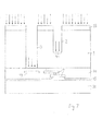
- Figure 1 shows a cross-section of an embodiment of the semiconductor device.
- a substrate 1 of semiconductor material which may be silicon and which may comprise an integrated circuit, is provided with a contact hole 2 and a via hole 3.
- the contact hole 2 reaches from a surface 10 of the substrate 1, which may be covered with a dielectric layer 5, vertically down into the substrate 1.
- the depth 22 of the contact hole 2 is less than the thickness of the substrate 1, including the thickness of the dielectric layer 5, so that a bottom area 40 of the contact hole 2 is formed by an internal surface of the semiconductor material within the substrate 1.
- a contact metalization 12 is located in the contact hole 2 and makes an internal substrate contact 4 on the semiconductor material of the substrate 1.
- the substrate contact 4 occupies at least the bottom area 40 of the contact hole 2.
- the semiconductor material adjacent to the substrate contact 4 is preferably doped and has a high doping concentration rendering a high electrical conductivity and a low-ohmic contact with the contact metalization 12.
- the via hole 3 penetrates the substrate 1 from the surface 10 to the opposite surface.
- a via metalization 13 is located in the via hole 3 and makes a contact on a terminal 19 arranged in a dielectric layer 14 at or near the opposite surface, thereby forming a through-substrate via.
- a wiring 9 can be embedded in the dielectric layer 14, which may be provided with a planarizing layer 15 on the side facing away from the substrate 1.
- the dielectric layers 5, 14 and the planarizing layer 15 can be an oxide of the semiconductor material, especially silicon dioxide.
- the depth 22 of the contact hole 2 may be typically about 110 ⁇ m and the depth 23 of the via hole 3 typically about 200 ⁇ m, for instance.
- a substrate edge 11 is indicated in Figure 1 as a line of reference facilitating a comparision with the plan views according to Figures 2 to 4 .
- the contact metalization 12 and the via metalization 13 are in contact with a suitably structured surface metal 7, which may be formed as an integral part of the metalizations 12, 13 or may be applied as a separate metal layer in contact with the metalizations 12, 13.
- the surface metal 7 may provide pads, especially a pad 17 that is connected with the via metalization 13.
- the surface metal 7 and the metalizations 12, 13 are preferably covered and protected with a passivation 8, which may have one or several openings for external electrical connection, especially above the pad 17.
- the contact metalization 12, the via metalization 13 or both the contact metalization 12 and the via metalization 13 can be insulated from the semiconductor material of the substrate 1 by a portion of the dielectric layer 5, which may be arranged on the walls of the contact hole 2 and the via hole 3.
- the bottom area 40 of the contact hole 2 is free from the dielectric layer 5 to accomodate the substrate contact 4.
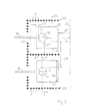
- Figure 2 shows a schematic plan view of an exemplary arrangement of contact holes 2 and via holes 3.
- the position of the cross-section shown in Figure 1 is indicated in Figure 2 by a broken line.
- the line on the right of Figure 2 indicates the substrate edge 11.
- the contact holes 2 are cylindrical and arranged in rows 20 along lines passing by the via holes 3, which are also cylindrical.
- the rows 20 of contact holes 2 are particularly arranged along lines surrounding the via holes 3 and separating the via holes 3 from one another.
- the via metalizations 13 are disposed on the walls of the via holes 3 and are connected with pads 17 arranged around the via holes 3.
- the rows 20 of contact holes 2 may completely surround the via holes 3.
- each of the pads 17 can be provided with an electrical connection inside the area that is surrounded by the rows 20 and encompasses the relevant pad 17.
- the rows 20 of contact holes 2 are preferably interrupted so that the conductor tracks 16 can pass between two sections of the rows 20 and connect the pads 17 with electrical connections arranged outside the area that is surrounded by the rows 20.
- the distance 24 between a via hole 3 and the closest edge of the appertaining pad 17 may be typically 10 ⁇ m.
- the distance 25 between a pad 17 and the substrate edge 11 may be typically 20 ⁇ m.
- the distance 26 between a via hole 3 and the substrate edge 11 may be typically 95 ⁇ m.
- the distance 27 between a via hole 3 and the closest row 20 of contact holes 2 may be typically 70 ⁇ m.
- the distance 28 between two neighboring pads 17 may be typically 60 ⁇ m.
- the distance 29 between a via hole 3 and the nearest further via hole 3 may be typically 150 ⁇ m.
- the distance 30 between opposite edges of a pad 17 may be typically 125 ⁇ m.
- the diameter 32 of the contact holes 2 may be typically 10 ⁇ m.
- the diameter 33 of the via holes 3 may be typically 40 ⁇ m.
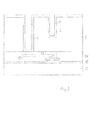
- Figure 3 shows a schematic plan view according to Figure 2 of an exemplary arrangement of contact holes that are formed by contact trenches 21 instead of cylindrical contact holes.
- the contact trenches 21 may be arranged with their longitudinal extensions along lines passing by the via holes 3, according to the rows 20 of cylindrical contact holes 2 in the embodiment according to Figure 2 .
- the distances 24, 25, 26, 27, 28, 29, 30 and the diameter 33 of the via holes 3 indicated in Figure 2 may be typically the same in the embodiment according to Figure 3 . If the depth of the contact trenches 21 substituting the rows 20 of cylindrical contact holes 2 is the same as the depth of the cylindrical contact holes 2, the width 32 of the contact trenches 21 is typically smaller than the width or diameter 32 of the cylindrical contact holes 2.
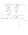
- Figure 4 shows a schematic plan view according to Figure 3 for a further embodiment, in which the contact trenches 21 are additionally arranged between the via holes 3 and the substrate edge 11.
- the distances 34 and 35 from the via hole 3 and the substrate edge 11, respectively, to an intermediate section of the contact trench 21, may both be typically 42,5 ⁇ m.
- the distance between the pads 17 and the substrate edge 11 is accordingly larger than in the preceding embodiments; the other distances may typically be as given above.
- Figure 5 shows a cross-section of an intermediate product of a method of producing the semiconductor device.
- a substrate 1 of semiconductor material which may be provided with an integrated circuit and a wiring 9 embedded in a dielectric layer 14, is used as a start material.
- an integrated circuit is supposed to be located at the substrate surface that is provided with the dielectric layer 14. Instead, the integrated circuit may be arranged at the upper substrate surface 10.
- a planarizing layer 15 may be provided to cover the dielectric layer 14 and any otherwise open contact areas on a metal layer of the wiring 9.
- the planarizing layer 15 may be an oxide of the semiconductor material, silicon dioxide for instance.
- the planarizing layer 15 serves as a bond layer to fasten a handling wafer 31 to the substrate 1.
- the planarizing layer 15 can be omitted if the dielectric layer 14 is used as a bond layer.
- the substrate 1 may then be thinned from the opposite side, until the surface 10 that is opposite to the integrated circuit reaches the position indicated in Figure 5 by a broken line.
- the substrate 1 is not thinned in this method step if there is an integrated circuit at the upper surface 10.
- the substrate 1 may in this case have been thinned before from the side that is opposite to the integrated circuit, particularly before the dielectric layer 14 was applied.
- Figure 6 shows a cross-section according to Figure 5 after the application of an etch mask 18 to the surface 10.
- the mask 18 has at least one small opening 37 of the lateral dimension 32 of the contact hole 2 and may furthermore have at least one large opening 38 for the lateral dimension 33 of the via hole 3.
- the mask 18 is used to etch the semiconductor material anisotropically to form holes having the dimensions that are indicated in Figure 6 by broken lines.
- DRIE deep reactive ion etching
- the opening 37 provided for the contact hole 2 should be smaller than the opening 38 provided for the via hole 3, but in variants of the method the DRIE etching recipe may be adapted to have an inverted aspect-ratio dependent etching (ARDE), which means that a larger mask opening produces a shallower hole than the smaller mask opening.
- ARDE inverted aspect-ratio dependent etching
- Figure 7 shows a cross-section according to Figure 6 after the etching of the contact hole 2 and the via hole 3.
- the arrows indicate an optional implantation of a dopant, which increases the electrical conductivity of the semiconductor material at the bottom area 40 of the contact hole 2 in order to improve the substrate contact 4.
- the implant is preferably annealed at an elevated temperature in the way that is known per se from the formation of doped regions in semiconductor material.
- Figure 8 shows a cross-section according to Figure 7 after the removal of the mask 18 and an application of a dielectric layer 5, which may be an oxide of the semiconductor material, silicon dioxide for instance.
- the dielectric layer 5 is provided to insulate the via metalization 13 from the semiconductor material at the wall of the via hole 3 and optionally also to insulate the contact metalization 12 from the semiconductor material at the wall of the contact hole 2.
- the dielectric layer 5 is removed at least from the bottom of the contact hole 2 and from the bottom of the via hole 3. This may be achieved by a standard anisotropic spacer etching.
- the dielectric layer 5 may completely be removed from the contact hole 2.
- the contact hole 2 may be covered by a mask while the dielectric layer 5 is formed in the via hole 3, so that the mask prevents the formation of a dielectric layer in the contact hole 2.
- Figure 9 shows a cross-section according to Figure 8 after an application of a contact metalization 12 in the contact hole 2 and a via metalization 13 in the via hole 3.
- the contact metalization 12 makes a contact on the semiconductor material within the substrate 1 at least in the bottom area 40 of the contact hole 2, where the electrical conductivity may optionally have been increased by the implantation mentioned above.
- a surface metal 7 may be applied as a separate layer and structured in sections that are in contact with the contact metalization 12 and the via metalization 13, respectively. Instead, the surface metal 7 may be structured out of an upper superficial portion of an initially entire metal layer that is deposited for the formation of both the contact metalization 12 and the via metalization 13. The surface metal 7 may particularly provide a pad 17.
- Figure 10 shows a cross-section according to Figure 8 for a further embodiment, in which the substrate 1 is a top wafer in combination with a bottom wafer 36 of semiconductor material.
- a dielectric layer 14 is arranged between the substrate 1 and the bottom wafer 36 and may comprise a wiring 9.
- the dielectric layer 14 may be formed on the top wafer, on the bottom wafer or partially on both wafers, before the wafers are bonded.
- an electronic circuit especially a CMOS circuit, may have been integrated, preferably before the contact hole 2 and the via hole 3 are etched.
- a dielectric layer 6 may be provided on the surface 10 as an intermetal dielectric for a wiring of the circuit, which is not shown in detail.
- Figure 10 shows the intermediate product after the deposition of the dielectric layer 5, which is subsequently removed from above the contact area of the terminal 19 and from the bottom area 40 of the contact hole 2. Then a contact metalization 12 and a via metalization 13 are applied according to the embodiment of Figure 9 .
- Figure 11 shows a cross-section according to Figure 1 for an embodiment which may be produced via the intermediate product shown in Figure 10 .
- the elements of this embodiment that are similar to elements of the embodiment according to Figure 1 are designated with the same reference numerals.
- the bottom wafer 36 of the embodiment according to Figure 11 is not removed like a handling wafer.
- the substrate 1 comprises the internal substrate contact 4 and a through-substrate via.
- the dielectric layer 14 may comprise a wiring 9 as shown in Figure 11 , which is provided as a rear wiring of the components of the circuit that are integrated at the upper surface 10.
- the substrate 1 may comprise a doped semiconductor material with a high doping concentration, which renders a low-ohmic contact of the contact metalization 12 on the semiconductor material and a favorably high electrical conductivity.
- a high doping concentration may not be appropriate for electronic components of the integrated circuit, which may especially be a CMOS circuit.
- the main portion of the substrate 1, which encompasses the region in which the internal substrate contact 4 is located, may nevertheless be highly doped if an epitaxial layer 39 that is undoped or moderately doped is epitaxially grown on the substrate 1 and the circuit components are integrated in the epitaxial layer 39.
- the internal substrate contact described above can easily be produced in conjunction with through-substrate vias and therefore provides an advantageous structure for an electrical protection around the through-substrate vias.
- Cross-talk and electrostatic damage can thus be prevented, particularly in applications comprising high signal frequencies.
- Further favorable applications include optical sensors or the like.
Landscapes
- Internal Circuitry In Semiconductor Integrated Circuit Devices (AREA)
Abstract
Description
- The invention relates to a semiconductor device with internal substrate contact, which is connected from a substrate surface, and particularly to a semiconductor device comprising an interconnect leading through the substrate like a through-silicon via, and to a method of producing a semiconductor device with an internal substrate contact.
- Applications of semiconductor devices may require that the substrate be maintained at a defined electric potential. To this end the substrate is often provided with an electrical contact at an outer surface, particularly the rear surface.
- In threedimensional integration semiconductor substrates that are provided with integrated circuits are stacked and bonded. The conductors that are arranged on different substrates are connected by interconnects leading through a substrate, especially through-silicon vias. The through-silicon vias are usually insulated from the semiconductor material of the substrate by a dielectric layer. Electric signals that are transmitted on a through-silicon via are inductively coupled through the dielectric layer to the semiconductor substrate. A small number of induced charge carriers suffice to generate a high voltage, which may be detrimental to many applications. It would be advantageous if the ground potential could be applied to the semiconductor material surrounding the through-silicon via in order to absorb the charge carriers and thus prevent cross-talk and electrostatic damage.
-
DE 10 2009 012 594 A1 describes a through-substrate interconnect having insulating and electrically conductive layers. A dielectric layer may be omitted and a metal liner arranged immediately at the wall of the via hole, particularly in applications wherein the interconnect is a ground connection. -
US 2010/0144114 A1 andUS 2011/0027962 A1 describe semiconductor devices having trenches of different depths, which are produced employing different vertical etch rates for differently dimensioned mask windows. - It is an object of this invention to disclose a new semiconductor device having a substrate contact and a related method of production.
- This object is achieved with the semiconductor device according to
claim 1 and with the method of producing a semiconductor device according to claim 8. Embodiments and alterations derive from the dependent claims. - The semiconductor device comprises a substrate of semiconductor material, a contact hole reaching from a surface of the substrate into the substrate, and a contact metalization arranged in the contact hole, so that the contact metalization makes an internal substrate contact on the semiconductor material at least in a bottom area of the contact hole.
- In an embodiment of the semiconductor device the substrate contact is limited by a dielectric layer arranged between the contact metalization and the semiconductor material of the substrate.
- A further embodiment comprises a plurality of similar further contact holes reaching from the substrate surface into the substrate, provided with contact metalizations that are arranged in the contact holes and make internal substrate contacts on the semiconductor material.
- The contact holes may especially be arranged in at least one row of contact holes. If the semiconductor device comprises a through-silicon via or, more generally, an interconnect leading through the substrate, which will in the following be called a through-substrate via, the row of contact holes may preferably be arranged along a line passing by the through-substrate via. The row of contact holes can especially be arranged surrounding the through-substrate via or separating two through-substrate vias from one another.
- In a further embodiment the contact hole is in the shape of a trench of longitudinal extension. If the semiconductor device comprises a through-substrate via, the contact trench may preferably be arranged along a line passing by the through-substrate via. The contact trench can especially be arranged surrounding the through-substrate via or separating two through-substrate vias from one another.
- A further embodiment comprises a via hole reaching from the substrate surface through the substrate to an opposite surface, thus penetrating the substrate. A via metalization is arranged in the via hole, forming a through-substrate via. The contact hole and the via hole have different widths.
- The method of producing a semiconductor device comprises the steps of providing a substrate of semiconductor material, etching a contact hole into the semiconductor material, and disposing a contact metalization in the contact hole in such a way that the contact metalization makes a substrate contact on the semiconductor material at least in a bottom area of the contact hole.
- A variant of the method comprises the use of a mask having at least a small opening and a large opening. The contact hole is etched through the small opening, and a via hole penetrating the substrate is etched through the large opening. Depending on the etch process, the contact hole may instead be etched through the large opening, whereas a via hole penetrating the substrate is etched through the small opening. A via metalization is disposed in the via hole.
- A further variant of the method comprises performing an implantation of a dopant through the contact hole into the semiconductor material of the substrate before applying the contact metalization.
- A further variant of the method comprises the use of a substrate of highly doped semiconductor material provided with an epitaxial layer of undoped or moderately doped semiconductor material. The substrate contact is formed on the highly doped semiconductor material.
- The following is a detailed description of exemplary embodiments of the semiconductor device and examples of the method of production in conjunction with the accompanying drawings.
-
Figure 1 shows a cross-section of an embodiment of the semiconductor device. -
Figure 2 shows a schematic plan view of an exemplary arrangement of cylindrical contact holes and via holes. -
Figure 3 shows a schematic plan view according toFigure 2 of an exemplary arrangement of trenchlike contact holes and cylindrical via holes. -
Figure 4 shows a schematic plan view according toFigure 3 for a further embodiment. -
Figure 5 shows a cross-section of an intermediate product of a method of producing the semiconductor device. -
Figure 6 shows a cross-section according toFigure 5 after the application of an etch mask. -
Figure 7 shows a cross-section according toFigure 6 after an etching step. -
Figure 8 shows a cross-section according toFigure 7 after an application of a dielectric layer. -
Figure 9 shows a cross-section according toFigure 8 after an application of metalizations. -
Figure 10 shows a cross-section according toFigure 8 for a further embodiment. -
Figure 11 shows a cross-section according toFigure 1 for a further embodiment. -
Figure 1 shows a cross-section of an embodiment of the semiconductor device. Asubstrate 1 of semiconductor material, which may be silicon and which may comprise an integrated circuit, is provided with acontact hole 2 and avia hole 3. - The
contact hole 2 reaches from asurface 10 of thesubstrate 1, which may be covered with adielectric layer 5, vertically down into thesubstrate 1. Thedepth 22 of thecontact hole 2 is less than the thickness of thesubstrate 1, including the thickness of thedielectric layer 5, so that abottom area 40 of thecontact hole 2 is formed by an internal surface of the semiconductor material within thesubstrate 1. Acontact metalization 12 is located in thecontact hole 2 and makes aninternal substrate contact 4 on the semiconductor material of thesubstrate 1. The substrate contact 4 occupies at least thebottom area 40 of thecontact hole 2. The semiconductor material adjacent to thesubstrate contact 4 is preferably doped and has a high doping concentration rendering a high electrical conductivity and a low-ohmic contact with thecontact metalization 12. - The
via hole 3 penetrates thesubstrate 1 from thesurface 10 to the opposite surface. Avia metalization 13 is located in thevia hole 3 and makes a contact on aterminal 19 arranged in adielectric layer 14 at or near the opposite surface, thereby forming a through-substrate via. A wiring 9 can be embedded in thedielectric layer 14, which may be provided with a planarizinglayer 15 on the side facing away from thesubstrate 1. Thedielectric layers layer 15 can be an oxide of the semiconductor material, especially silicon dioxide. - The
depth 22 of thecontact hole 2 may be typically about 110 µm and thedepth 23 of thevia hole 3 typically about 200 µm, for instance. Asubstrate edge 11 is indicated inFigure 1 as a line of reference facilitating a comparision with the plan views according toFigures 2 to 4 . - The
contact metalization 12 and thevia metalization 13 are in contact with a suitably structured surface metal 7, which may be formed as an integral part of themetalizations metalizations pad 17 that is connected with thevia metalization 13. The surface metal 7 and themetalizations pad 17. - The
contact metalization 12, thevia metalization 13 or both thecontact metalization 12 and thevia metalization 13 can be insulated from the semiconductor material of thesubstrate 1 by a portion of thedielectric layer 5, which may be arranged on the walls of thecontact hole 2 and thevia hole 3. Thebottom area 40 of thecontact hole 2 is free from thedielectric layer 5 to accomodate thesubstrate contact 4. -
Figure 2 shows a schematic plan view of an exemplary arrangement ofcontact holes 2 and viaholes 3. The position of the cross-section shown inFigure 1 is indicated inFigure 2 by a broken line. The line on the right ofFigure 2 indicates thesubstrate edge 11. In the embodiment according toFigure 2 , the contact holes 2 are cylindrical and arranged inrows 20 along lines passing by the via holes 3, which are also cylindrical. Therows 20 ofcontact holes 2 are particularly arranged along lines surrounding the via holes 3 and separating the via holes 3 from one another. The via metalizations 13 are disposed on the walls of the via holes 3 and are connected withpads 17 arranged around the via holes 3. - The
rows 20 ofcontact holes 2 may completely surround the via holes 3. In this case each of thepads 17 can be provided with an electrical connection inside the area that is surrounded by therows 20 and encompasses therelevant pad 17. If instead conductor tracks 16 leading out of this area are provided for thepads 17, as shown inFigure 2 , therows 20 ofcontact holes 2 are preferably interrupted so that the conductor tracks 16 can pass between two sections of therows 20 and connect thepads 17 with electrical connections arranged outside the area that is surrounded by therows 20. - The
distance 24 between a viahole 3 and the closest edge of the appertainingpad 17 may be typically 10 µm. Thedistance 25 between apad 17 and thesubstrate edge 11 may be typically 20 µm. Thedistance 26 between a viahole 3 and thesubstrate edge 11 may be typically 95 µm. The distance 27 between a viahole 3 and theclosest row 20 ofcontact holes 2 may be typically 70 µm. Thedistance 28 between two neighboringpads 17 may be typically 60 µm. Thedistance 29 between a viahole 3 and the nearest further viahole 3 may be typically 150 µm. Thedistance 30 between opposite edges of apad 17 may be typically 125 µm. Thediameter 32 of the contact holes 2 may be typically 10 µm. Thediameter 33 of the via holes 3 may be typically 40 µm. -
Figure 3 shows a schematic plan view according toFigure 2 of an exemplary arrangement of contact holes that are formed bycontact trenches 21 instead of cylindrical contact holes. Thecontact trenches 21 may be arranged with their longitudinal extensions along lines passing by the via holes 3, according to therows 20 of cylindrical contact holes 2 in the embodiment according toFigure 2 . Thedistances diameter 33 of the via holes 3 indicated inFigure 2 may be typically the same in the embodiment according toFigure 3 . If the depth of thecontact trenches 21 substituting therows 20 of cylindrical contact holes 2 is the same as the depth of the cylindrical contact holes 2, thewidth 32 of thecontact trenches 21 is typically smaller than the width ordiameter 32 of the cylindrical contact holes 2. -
Figure 4 shows a schematic plan view according toFigure 3 for a further embodiment, in which thecontact trenches 21 are additionally arranged between the via holes 3 and thesubstrate edge 11. Thedistances hole 3 and thesubstrate edge 11, respectively, to an intermediate section of thecontact trench 21, may both be typically 42,5 µm. The distance between thepads 17 and thesubstrate edge 11 is accordingly larger than in the preceding embodiments; the other distances may typically be as given above. -
Figure 5 shows a cross-section of an intermediate product of a method of producing the semiconductor device. Asubstrate 1 of semiconductor material, which may be provided with an integrated circuit and a wiring 9 embedded in adielectric layer 14, is used as a start material. In the example shown inFigure 5 an integrated circuit is supposed to be located at the substrate surface that is provided with thedielectric layer 14. Instead, the integrated circuit may be arranged at theupper substrate surface 10. Aplanarizing layer 15 may be provided to cover thedielectric layer 14 and any otherwise open contact areas on a metal layer of the wiring 9. Theplanarizing layer 15 may be an oxide of the semiconductor material, silicon dioxide for instance. Theplanarizing layer 15 serves as a bond layer to fasten a handlingwafer 31 to thesubstrate 1. Theplanarizing layer 15 can be omitted if thedielectric layer 14 is used as a bond layer. Thesubstrate 1 may then be thinned from the opposite side, until thesurface 10 that is opposite to the integrated circuit reaches the position indicated inFigure 5 by a broken line. Thesubstrate 1 is not thinned in this method step if there is an integrated circuit at theupper surface 10. Thesubstrate 1 may in this case have been thinned before from the side that is opposite to the integrated circuit, particularly before thedielectric layer 14 was applied. -
Figure 6 shows a cross-section according toFigure 5 after the application of anetch mask 18 to thesurface 10. Themask 18 has at least onesmall opening 37 of thelateral dimension 32 of thecontact hole 2 and may furthermore have at least onelarge opening 38 for thelateral dimension 33 of the viahole 3. Themask 18 is used to etch the semiconductor material anisotropically to form holes having the dimensions that are indicated inFigure 6 by broken lines. - Different depths of the holes can easily be achieved with an etch process like deep reactive ion etching (DRIE), which enables different vertical etch rates depending on the lateral dimensions of the
mask openings opening 37 provided for thecontact hole 2 should be smaller than theopening 38 provided for the viahole 3, but in variants of the method the DRIE etching recipe may be adapted to have an inverted aspect-ratio dependent etching (ARDE), which means that a larger mask opening produces a shallower hole than the smaller mask opening. In the following the method is explained for the typical examples in which the larger mask opening produces a deeper hole than the smaller mask opening. -
Figure 7 shows a cross-section according toFigure 6 after the etching of thecontact hole 2 and the viahole 3. The arrows indicate an optional implantation of a dopant, which increases the electrical conductivity of the semiconductor material at thebottom area 40 of thecontact hole 2 in order to improve thesubstrate contact 4. The implant is preferably annealed at an elevated temperature in the way that is known per se from the formation of doped regions in semiconductor material. -
Figure 8 shows a cross-section according toFigure 7 after the removal of themask 18 and an application of adielectric layer 5, which may be an oxide of the semiconductor material, silicon dioxide for instance. Thedielectric layer 5 is provided to insulate the viametalization 13 from the semiconductor material at the wall of the viahole 3 and optionally also to insulate thecontact metalization 12 from the semiconductor material at the wall of thecontact hole 2. - The
dielectric layer 5 is removed at least from the bottom of thecontact hole 2 and from the bottom of the viahole 3. This may be achieved by a standard anisotropic spacer etching. Thedielectric layer 5 may completely be removed from thecontact hole 2. Instead, thecontact hole 2 may be covered by a mask while thedielectric layer 5 is formed in the viahole 3, so that the mask prevents the formation of a dielectric layer in thecontact hole 2. In an embodiment according toFigure 8 it may be necessary to remove a portion of thedielectric layer 14 from the contact area of the terminal 19 before the viametalization 13 is applied. -
Figure 9 shows a cross-section according toFigure 8 after an application of acontact metalization 12 in thecontact hole 2 and a viametalization 13 in the viahole 3. Thecontact metalization 12 makes a contact on the semiconductor material within thesubstrate 1 at least in thebottom area 40 of thecontact hole 2, where the electrical conductivity may optionally have been increased by the implantation mentioned above. - A surface metal 7 may be applied as a separate layer and structured in sections that are in contact with the
contact metalization 12 and the viametalization 13, respectively. Instead, the surface metal 7 may be structured out of an upper superficial portion of an initially entire metal layer that is deposited for the formation of both thecontact metalization 12 and the viametalization 13. The surface metal 7 may particularly provide apad 17. -
Figure 10 shows a cross-section according toFigure 8 for a further embodiment, in which thesubstrate 1 is a top wafer in combination with abottom wafer 36 of semiconductor material. Adielectric layer 14 is arranged between thesubstrate 1 and thebottom wafer 36 and may comprise a wiring 9. Thedielectric layer 14 may be formed on the top wafer, on the bottom wafer or partially on both wafers, before the wafers are bonded. At thesubstrate surface 10 facing away from thebottom wafer 36, an electronic circuit, especially a CMOS circuit, may have been integrated, preferably before thecontact hole 2 and the viahole 3 are etched. Adielectric layer 6 may be provided on thesurface 10 as an intermetal dielectric for a wiring of the circuit, which is not shown in detail. -
Figure 10 shows the intermediate product after the deposition of thedielectric layer 5, which is subsequently removed from above the contact area of the terminal 19 and from thebottom area 40 of thecontact hole 2. Then acontact metalization 12 and a viametalization 13 are applied according to the embodiment ofFigure 9 . -
Figure 11 shows a cross-section according toFigure 1 for an embodiment which may be produced via the intermediate product shown inFigure 10 . The elements of this embodiment that are similar to elements of the embodiment according toFigure 1 are designated with the same reference numerals. Thebottom wafer 36 of the embodiment according toFigure 11 is not removed like a handling wafer. Thesubstrate 1 comprises theinternal substrate contact 4 and a through-substrate via. Thedielectric layer 14 may comprise a wiring 9 as shown inFigure 11 , which is provided as a rear wiring of the components of the circuit that are integrated at theupper surface 10. - The
substrate 1 may comprise a doped semiconductor material with a high doping concentration, which renders a low-ohmic contact of thecontact metalization 12 on the semiconductor material and a favorably high electrical conductivity. Such a high doping concentration may not be appropriate for electronic components of the integrated circuit, which may especially be a CMOS circuit. In this case the main portion of thesubstrate 1, which encompasses the region in which theinternal substrate contact 4 is located, may nevertheless be highly doped if anepitaxial layer 39 that is undoped or moderately doped is epitaxially grown on thesubstrate 1 and the circuit components are integrated in theepitaxial layer 39. - The internal substrate contact described above can easily be produced in conjunction with through-substrate vias and therefore provides an advantageous structure for an electrical protection around the through-substrate vias. Cross-talk and electrostatic damage can thus be prevented, particularly in applications comprising high signal frequencies. Further favorable applications include optical sensors or the like.
- List of reference numerals
- 1
- substrate
- 2
- contact hole
- 3
- via hole
- 4
- substrate contact
- 5
- dielectric layer
- 6
- dielectric layer
- 7
- surface metal
- 8
- passivation
- 9
- wiring
- 10
- substrate surface
- 11
- substrate edge
- 12
- contact metalization
- 13
- via metalization
- 14
- dielectric layer
- 15
- planarizing layer
- 16
- conductor track
- 17
- pad
- 18
- mask
- 19
- terminal
- 20
- row of contact holes
- 21
- contact trench
- 22
- depth of the contact hole
- 23
- depth of the via hole
- 24
- distance
- 25
- distance
- 26
- distance
- 27
- distance
- 28
- distance
- 29
- distance
- 30
- distance
- 31
- handling wafer
- 32
- width or diameter of the contact hole
- 32'
- width of the contact trench
- 33
- width or diameter of the via hole
- 34
- distance
- 35
- distance
- 36
- bottom wafer
- 37
- small opening
- 38
- large opening
- 39
- epitaxial layer
- 40
- bottom area
Claims (12)
- A semiconductor device comprising:- a substrate (1) of semiconductor material with a surface (10),- a contact hole (2) reaching from the substrate surface (10) into the substrate (1), and- a contact metalization (12) in the contact hole (2), characterized in that- the contact metalization (12) makes a substrate contact (4) on the semiconductor material, and- the substrate contact (4) occupies at least a bottom area (40) of the contact hole (2).
- The semiconductor device of claim 1, wherein
the substrate contact (4) is limited by a dielectric layer (5) arranged between the contact metalization (12) and the semiconductor material of the substrate (1). - The semiconductor device of claim 1 or 2, further comprising:a plurality of further contact holes (2) reaching from the substrate surface (10) into the substrate (1), with contact metalizations (12) in the contact holes (2) making substrate contacts (4) on the semiconductor material,the contact holes (2) being arranged in at least one row (20) of contact holes (2).
- The semiconductor device of claim 3, further comprising a through-substrate via (3, 13), the row (20) of contact holes (2) being arranged along a line passing by the through-substrate via (3, 13).
- The semiconductor device of claim 3, wherein
the contact hole (2) is in the shape of a contact trench (21) of longitudinal extension. - The semiconductor device of claim 5, further comprising a through-substrate via (3, 13), the contact trench (21) being arranged along a line passing by the through-substrate Via (3, 13).
- The semiconductor device of one of claims 1 to 6, comprising:- a via hole (3) penetrating the substrate (1) from the substrate surface (10), and- a via metalization (13) in the via hole (3),- the contact hole (2) and the via hole (3) having different widths or diameters (32, 33).
- A method of producing a semiconductor device, comprising:- providing a substrate (1) of semiconductor material,- etching a contact hole (2) into the substrate (1), and- disposing a contact metalization (12) in the contact hole (2),
characterized in that- the contact metalization (12) is applied making a substrate contact (4) on the semiconductor material at least in a bottom area (40) of the contact hole (2). - The method of claim 8, further comprising:using a mask (18) having at least a small opening (37) and a large opening (38),etching the contact hole (2) through the small opening (37) and a via hole (3) penetrating the substrate (1) through the large opening (38), anddisposing a via metalization (13) in the via hole (3).
- The method of claim 8, further comprising:using a mask (18) having at least a small opening (37) and a large opening (38),etching the contact hole (2) through the large opening (38) and a via hole (3) penetrating the substrate (1) through the small opening (37), anddisposing a via metalization (13) in the via hole (3).
- The method of one of claims 8 to 10, further comprising:performing an implantation of a dopant through the contact hole (2) into the semiconductor material of the substrate (1) before the disposition of the contact metalization (12).
- The method of one of claims 8 to 10, further comprising:providing the substrate (1) with a high doping and with an epitaxial layer (39) of undoped or moderately doped semiconductor material, andmaking the substrate contact (4) on the highly doped semiconductor material.
Priority Applications (3)
| Application Number | Priority Date | Filing Date | Title |
|---|---|---|---|
| EP12152485.4A EP2620978B1 (en) | 2012-01-25 | 2012-01-25 | Semiconductor device with internal substrate contact and method of production |
| US14/373,627 US9245843B2 (en) | 2012-01-25 | 2013-01-16 | Semiconductor device with internal substrate contact and method of production |
| PCT/EP2013/050736 WO2013110533A1 (en) | 2012-01-25 | 2013-01-16 | Semiconductor device with internal substrate contact and method of production |
Applications Claiming Priority (1)
| Application Number | Priority Date | Filing Date | Title |
|---|---|---|---|
| EP12152485.4A EP2620978B1 (en) | 2012-01-25 | 2012-01-25 | Semiconductor device with internal substrate contact and method of production |
Publications (2)
| Publication Number | Publication Date |
|---|---|
| EP2620978A1 true EP2620978A1 (en) | 2013-07-31 |
| EP2620978B1 EP2620978B1 (en) | 2019-07-24 |
Family
ID=47561628
Family Applications (1)
| Application Number | Title | Priority Date | Filing Date |
|---|---|---|---|
| EP12152485.4A Active EP2620978B1 (en) | 2012-01-25 | 2012-01-25 | Semiconductor device with internal substrate contact and method of production |
Country Status (3)
| Country | Link |
|---|---|
| US (1) | US9245843B2 (en) |
| EP (1) | EP2620978B1 (en) |
| WO (1) | WO2013110533A1 (en) |
Cited By (2)
| Publication number | Priority date | Publication date | Assignee | Title |
|---|---|---|---|---|
| WO2015055480A1 (en) * | 2013-10-14 | 2015-04-23 | Ams Ag | Semiconductor device with optical and electrical vias |
| WO2015121199A3 (en) * | 2014-02-12 | 2015-11-19 | Ams Ag | Semiconductor device with a bump contact on a tsv comprising a cavity and method of producing such a semiconductor device |
Families Citing this family (5)
| Publication number | Priority date | Publication date | Assignee | Title |
|---|---|---|---|---|
| US9202792B2 (en) * | 2014-04-25 | 2015-12-01 | Taiwan Semiconductor Manufacturing Company Limited | Structure and method of providing a re-distribution layer (RDL) and a through-silicon via (TSV) |
| EP3471132B1 (en) * | 2017-10-12 | 2020-02-26 | ams AG | Method for manufacturing a semiconductor device and semiconductor device |
| WO2022202015A1 (en) * | 2021-03-24 | 2022-09-29 | ソニーセミコンダクタソリューションズ株式会社 | Semiconductor device and semiconductor device manufacturing method |
| US20230062967A1 (en) * | 2021-08-31 | 2023-03-02 | Nanya Technology Corporation | Semiconductor device with contacts having different dimensions and method for fabricating the same |
| DE102024200633A1 (en) | 2024-01-24 | 2025-07-24 | Fraunhofer-Gesellschaft zur Förderung der angewandten Forschung eingetragener Verein | Vertical wiring of a semiconductor device |
Citations (5)
| Publication number | Priority date | Publication date | Assignee | Title |
|---|---|---|---|---|
| WO2008058829A1 (en) * | 2006-11-17 | 2008-05-22 | Austriamicrosystems Ag | Method for producing a semiconductor component with two trenches |
| DE102009012594A1 (en) | 2008-06-06 | 2009-12-24 | Infineon Technologies Ag | Through substrate via semiconductor components |
| US20100109114A1 (en) * | 2008-11-05 | 2010-05-06 | Oki Semiconductor Co., Ltd. | Semiconductor device and manufacturing method thereof |
| US20110018109A1 (en) * | 2009-07-22 | 2011-01-27 | Newport Fab, Llc Dba Jazz Semiconductor | Deep silicon via for grounding of circuits and devices, emitter ballasting and isolation |
| US20110027962A1 (en) | 2009-07-29 | 2011-02-03 | International Business Machines Corporation | Trench decoupling capacitor formed by rie lag of through silicon via (tsv) etch |
-
2012
- 2012-01-25 EP EP12152485.4A patent/EP2620978B1/en active Active
-
2013
- 2013-01-16 US US14/373,627 patent/US9245843B2/en active Active
- 2013-01-16 WO PCT/EP2013/050736 patent/WO2013110533A1/en not_active Ceased
Patent Citations (6)
| Publication number | Priority date | Publication date | Assignee | Title |
|---|---|---|---|---|
| WO2008058829A1 (en) * | 2006-11-17 | 2008-05-22 | Austriamicrosystems Ag | Method for producing a semiconductor component with two trenches |
| US20100144114A1 (en) | 2006-11-17 | 2010-06-10 | Austriamicroystems Ag | Method for Producing a Semiconductor Component with Two Trenches |
| DE102009012594A1 (en) | 2008-06-06 | 2009-12-24 | Infineon Technologies Ag | Through substrate via semiconductor components |
| US20100109114A1 (en) * | 2008-11-05 | 2010-05-06 | Oki Semiconductor Co., Ltd. | Semiconductor device and manufacturing method thereof |
| US20110018109A1 (en) * | 2009-07-22 | 2011-01-27 | Newport Fab, Llc Dba Jazz Semiconductor | Deep silicon via for grounding of circuits and devices, emitter ballasting and isolation |
| US20110027962A1 (en) | 2009-07-29 | 2011-02-03 | International Business Machines Corporation | Trench decoupling capacitor formed by rie lag of through silicon via (tsv) etch |
Cited By (4)
| Publication number | Priority date | Publication date | Assignee | Title |
|---|---|---|---|---|
| WO2015055480A1 (en) * | 2013-10-14 | 2015-04-23 | Ams Ag | Semiconductor device with optical and electrical vias |
| US9995894B2 (en) | 2013-10-14 | 2018-06-12 | Ams Ag | Semiconductor device with optical and electrical vias |
| WO2015121199A3 (en) * | 2014-02-12 | 2015-11-19 | Ams Ag | Semiconductor device with a bump contact on a tsv comprising a cavity and method of producing such a semiconductor device |
| US10217715B2 (en) | 2014-02-12 | 2019-02-26 | Ams Ag | Semiconductor device with a bump contact on a TSV comprising a cavity and method of producing such a semiconductor device |
Also Published As
| Publication number | Publication date |
|---|---|
| WO2013110533A1 (en) | 2013-08-01 |
| US20140367862A1 (en) | 2014-12-18 |
| EP2620978B1 (en) | 2019-07-24 |
| US9245843B2 (en) | 2016-01-26 |
Similar Documents
| Publication | Publication Date | Title |
|---|---|---|
| US9245843B2 (en) | Semiconductor device with internal substrate contact and method of production | |
| US9269664B2 (en) | Semiconductor package with through silicon via interconnect and method for fabricating the same | |
| US8445995B2 (en) | Semiconductor structure with conductive plug in an oxide layer | |
| KR20190087843A (en) | Semiconductor device | |
| KR101791730B1 (en) | Semiconductor structure and fabricating method thereof | |
| US20200411414A1 (en) | Through semiconductor via structure with reduced stress proximity effect | |
| KR20200145102A (en) | Vertical memory devices | |
| US20160155685A1 (en) | Through-substrate structure and mehtod for fabricating the same | |
| EP2887387A1 (en) | Semiconductor device and associated method | |
| US8969193B2 (en) | Method of producing a semiconductor device having an interconnect through the substrate | |
| US9837305B1 (en) | Forming deep airgaps without flop over | |
| CN106876318B (en) | Semiconductor device and method for manufacturing the same | |
| TWI674626B (en) | Electronic device including a material defining a void and a process of forming the same | |
| EP1935008B1 (en) | Microelectronic assembly and method for forming the same | |
| JP2006012953A (en) | Method for forming through electrode, through electrode and semiconductor device | |
| EP3312874A1 (en) | Method of forming a through-substrate via and a semiconductor device comprising a through-substrate via | |
| CN108511415B (en) | Method for manufacturing electronic assembly | |
| CN108231737B (en) | TSV with Improved Substrate Contact for Reducing TSV Capacitance Variability | |
| US20240170371A1 (en) | Semiconductor substrate comprising a through-substrate-via and method for producing thereof | |
| US7485926B2 (en) | SOI contact structures | |
| TWI552285B (en) | Semiconductor component and method of manufacturing same | |
| US8384214B2 (en) | Semiconductor structure, pad structure and protection structure | |
| EP2648214B1 (en) | Methods of producing a semiconductor device with a through-substrate via | |
| EP2790211A1 (en) | Method of producing a through-substrate via in a semiconductor device and semiconductor device comprising a through-substrate via | |
| US20140246777A1 (en) | Controlled metal extrusion opening in semiconductor structure and method of forming |
Legal Events
| Date | Code | Title | Description |
|---|---|---|---|
| PUAI | Public reference made under article 153(3) epc to a published international application that has entered the european phase |
Free format text: ORIGINAL CODE: 0009012 |
|
| AK | Designated contracting states |
Kind code of ref document: A1 Designated state(s): AL AT BE BG CH CY CZ DE DK EE ES FI FR GB GR HR HU IE IS IT LI LT LU LV MC MK MT NL NO PL PT RO RS SE SI SK SM TR |
|
| AX | Request for extension of the european patent |
Extension state: BA ME |
|
| 17P | Request for examination filed |
Effective date: 20140113 |
|
| RBV | Designated contracting states (corrected) |
Designated state(s): AL AT BE BG CH CY CZ DE DK EE ES FI FR GB GR HR HU IE IS IT LI LT LU LV MC MK MT NL NO PL PT RO RS SE SI SK SM TR |
|
| STAA | Information on the status of an ep patent application or granted ep patent |
Free format text: STATUS: EXAMINATION IS IN PROGRESS |
|
| 17Q | First examination report despatched |
Effective date: 20170131 |
|
| GRAP | Despatch of communication of intention to grant a patent |
Free format text: ORIGINAL CODE: EPIDOSNIGR1 |
|
| STAA | Information on the status of an ep patent application or granted ep patent |
Free format text: STATUS: GRANT OF PATENT IS INTENDED |
|
| INTG | Intention to grant announced |
Effective date: 20190215 |
|
| GRAS | Grant fee paid |
Free format text: ORIGINAL CODE: EPIDOSNIGR3 |
|
| GRAA | (expected) grant |
Free format text: ORIGINAL CODE: 0009210 |
|
| STAA | Information on the status of an ep patent application or granted ep patent |
Free format text: STATUS: THE PATENT HAS BEEN GRANTED |
|
| AK | Designated contracting states |
Kind code of ref document: B1 Designated state(s): AL AT BE BG CH CY CZ DE DK EE ES FI FR GB GR HR HU IE IS IT LI LT LU LV MC MK MT NL NO PL PT RO RS SE SI SK SM TR |
|
| RAP1 | Party data changed (applicant data changed or rights of an application transferred) |
Owner name: AUSTRIAMICROSYSTEMS AG |
|
| REG | Reference to a national code |
Ref country code: GB Ref legal event code: FG4D |
|
| REG | Reference to a national code |
Ref country code: CH Ref legal event code: EP |
|
| REG | Reference to a national code |
Ref country code: DE Ref legal event code: R096 Ref document number: 602012062186 Country of ref document: DE |
|
| REG | Reference to a national code |
Ref country code: AT Ref legal event code: REF Ref document number: 1159217 Country of ref document: AT Kind code of ref document: T Effective date: 20190815 |
|
| REG | Reference to a national code |
Ref country code: DE Ref legal event code: R081 Ref document number: 602012062186 Country of ref document: DE Owner name: AMS AG, AT Free format text: FORMER OWNER: AUSTRIAMICROSYSTEMS AG, PREMSTAETTEN, AT |
|
| REG | Reference to a national code |
Ref country code: IE Ref legal event code: FG4D |
|
| REG | Reference to a national code |
Ref country code: NL Ref legal event code: MP Effective date: 20190724 |
|
| REG | Reference to a national code |
Ref country code: LT Ref legal event code: MG4D |
|
| REG | Reference to a national code |
Ref country code: AT Ref legal event code: MK05 Ref document number: 1159217 Country of ref document: AT Kind code of ref document: T Effective date: 20190724 |
|
| PG25 | Lapsed in a contracting state [announced via postgrant information from national office to epo] |
Ref country code: AT Free format text: LAPSE BECAUSE OF FAILURE TO SUBMIT A TRANSLATION OF THE DESCRIPTION OR TO PAY THE FEE WITHIN THE PRESCRIBED TIME-LIMIT Effective date: 20190724 Ref country code: NO Free format text: LAPSE BECAUSE OF FAILURE TO SUBMIT A TRANSLATION OF THE DESCRIPTION OR TO PAY THE FEE WITHIN THE PRESCRIBED TIME-LIMIT Effective date: 20191024 Ref country code: HR Free format text: LAPSE BECAUSE OF FAILURE TO SUBMIT A TRANSLATION OF THE DESCRIPTION OR TO PAY THE FEE WITHIN THE PRESCRIBED TIME-LIMIT Effective date: 20190724 Ref country code: SE Free format text: LAPSE BECAUSE OF FAILURE TO SUBMIT A TRANSLATION OF THE DESCRIPTION OR TO PAY THE FEE WITHIN THE PRESCRIBED TIME-LIMIT Effective date: 20190724 Ref country code: FI Free format text: LAPSE BECAUSE OF FAILURE TO SUBMIT A TRANSLATION OF THE DESCRIPTION OR TO PAY THE FEE WITHIN THE PRESCRIBED TIME-LIMIT Effective date: 20190724 Ref country code: LT Free format text: LAPSE BECAUSE OF FAILURE TO SUBMIT A TRANSLATION OF THE DESCRIPTION OR TO PAY THE FEE WITHIN THE PRESCRIBED TIME-LIMIT Effective date: 20190724 Ref country code: PT Free format text: LAPSE BECAUSE OF FAILURE TO SUBMIT A TRANSLATION OF THE DESCRIPTION OR TO PAY THE FEE WITHIN THE PRESCRIBED TIME-LIMIT Effective date: 20191125 Ref country code: NL Free format text: LAPSE BECAUSE OF FAILURE TO SUBMIT A TRANSLATION OF THE DESCRIPTION OR TO PAY THE FEE WITHIN THE PRESCRIBED TIME-LIMIT Effective date: 20190724 Ref country code: BG Free format text: LAPSE BECAUSE OF FAILURE TO SUBMIT A TRANSLATION OF THE DESCRIPTION OR TO PAY THE FEE WITHIN THE PRESCRIBED TIME-LIMIT Effective date: 20191024 |
|
| PG25 | Lapsed in a contracting state [announced via postgrant information from national office to epo] |
Ref country code: GR Free format text: LAPSE BECAUSE OF FAILURE TO SUBMIT A TRANSLATION OF THE DESCRIPTION OR TO PAY THE FEE WITHIN THE PRESCRIBED TIME-LIMIT Effective date: 20191025 Ref country code: LV Free format text: LAPSE BECAUSE OF FAILURE TO SUBMIT A TRANSLATION OF THE DESCRIPTION OR TO PAY THE FEE WITHIN THE PRESCRIBED TIME-LIMIT Effective date: 20190724 Ref country code: ES Free format text: LAPSE BECAUSE OF FAILURE TO SUBMIT A TRANSLATION OF THE DESCRIPTION OR TO PAY THE FEE WITHIN THE PRESCRIBED TIME-LIMIT Effective date: 20190724 Ref country code: AL Free format text: LAPSE BECAUSE OF FAILURE TO SUBMIT A TRANSLATION OF THE DESCRIPTION OR TO PAY THE FEE WITHIN THE PRESCRIBED TIME-LIMIT Effective date: 20190724 Ref country code: RS Free format text: LAPSE BECAUSE OF FAILURE TO SUBMIT A TRANSLATION OF THE DESCRIPTION OR TO PAY THE FEE WITHIN THE PRESCRIBED TIME-LIMIT Effective date: 20190724 Ref country code: IS Free format text: LAPSE BECAUSE OF FAILURE TO SUBMIT A TRANSLATION OF THE DESCRIPTION OR TO PAY THE FEE WITHIN THE PRESCRIBED TIME-LIMIT Effective date: 20191124 |
|
| PG25 | Lapsed in a contracting state [announced via postgrant information from national office to epo] |
Ref country code: TR Free format text: LAPSE BECAUSE OF FAILURE TO SUBMIT A TRANSLATION OF THE DESCRIPTION OR TO PAY THE FEE WITHIN THE PRESCRIBED TIME-LIMIT Effective date: 20190724 |
|
| PG25 | Lapsed in a contracting state [announced via postgrant information from national office to epo] |
Ref country code: RO Free format text: LAPSE BECAUSE OF FAILURE TO SUBMIT A TRANSLATION OF THE DESCRIPTION OR TO PAY THE FEE WITHIN THE PRESCRIBED TIME-LIMIT Effective date: 20190724 Ref country code: PL Free format text: LAPSE BECAUSE OF FAILURE TO SUBMIT A TRANSLATION OF THE DESCRIPTION OR TO PAY THE FEE WITHIN THE PRESCRIBED TIME-LIMIT Effective date: 20190724 Ref country code: EE Free format text: LAPSE BECAUSE OF FAILURE TO SUBMIT A TRANSLATION OF THE DESCRIPTION OR TO PAY THE FEE WITHIN THE PRESCRIBED TIME-LIMIT Effective date: 20190724 Ref country code: DK Free format text: LAPSE BECAUSE OF FAILURE TO SUBMIT A TRANSLATION OF THE DESCRIPTION OR TO PAY THE FEE WITHIN THE PRESCRIBED TIME-LIMIT Effective date: 20190724 Ref country code: IT Free format text: LAPSE BECAUSE OF FAILURE TO SUBMIT A TRANSLATION OF THE DESCRIPTION OR TO PAY THE FEE WITHIN THE PRESCRIBED TIME-LIMIT Effective date: 20190724 |
|
| PG25 | Lapsed in a contracting state [announced via postgrant information from national office to epo] |
Ref country code: IS Free format text: LAPSE BECAUSE OF FAILURE TO SUBMIT A TRANSLATION OF THE DESCRIPTION OR TO PAY THE FEE WITHIN THE PRESCRIBED TIME-LIMIT Effective date: 20200224 Ref country code: SM Free format text: LAPSE BECAUSE OF FAILURE TO SUBMIT A TRANSLATION OF THE DESCRIPTION OR TO PAY THE FEE WITHIN THE PRESCRIBED TIME-LIMIT Effective date: 20190724 Ref country code: SK Free format text: LAPSE BECAUSE OF FAILURE TO SUBMIT A TRANSLATION OF THE DESCRIPTION OR TO PAY THE FEE WITHIN THE PRESCRIBED TIME-LIMIT Effective date: 20190724 Ref country code: CZ Free format text: LAPSE BECAUSE OF FAILURE TO SUBMIT A TRANSLATION OF THE DESCRIPTION OR TO PAY THE FEE WITHIN THE PRESCRIBED TIME-LIMIT Effective date: 20190724 |
|
| REG | Reference to a national code |
Ref country code: DE Ref legal event code: R097 Ref document number: 602012062186 Country of ref document: DE |
|
| PLBE | No opposition filed within time limit |
Free format text: ORIGINAL CODE: 0009261 |
|
| STAA | Information on the status of an ep patent application or granted ep patent |
Free format text: STATUS: NO OPPOSITION FILED WITHIN TIME LIMIT |
|
| PG2D | Information on lapse in contracting state deleted |
Ref country code: IS |
|
| 26N | No opposition filed |
Effective date: 20200603 |
|
| PG25 | Lapsed in a contracting state [announced via postgrant information from national office to epo] |
Ref country code: MC Free format text: LAPSE BECAUSE OF FAILURE TO SUBMIT A TRANSLATION OF THE DESCRIPTION OR TO PAY THE FEE WITHIN THE PRESCRIBED TIME-LIMIT Effective date: 20190724 Ref country code: SI Free format text: LAPSE BECAUSE OF FAILURE TO SUBMIT A TRANSLATION OF THE DESCRIPTION OR TO PAY THE FEE WITHIN THE PRESCRIBED TIME-LIMIT Effective date: 20190724 |
|
| REG | Reference to a national code |
Ref country code: CH Ref legal event code: PL |
|
| GBPC | Gb: european patent ceased through non-payment of renewal fee |
Effective date: 20200125 |
|
| REG | Reference to a national code |
Ref country code: BE Ref legal event code: MM Effective date: 20200131 |
|
| PG25 | Lapsed in a contracting state [announced via postgrant information from national office to epo] |
Ref country code: GB Free format text: LAPSE BECAUSE OF NON-PAYMENT OF DUE FEES Effective date: 20200125 Ref country code: LU Free format text: LAPSE BECAUSE OF NON-PAYMENT OF DUE FEES Effective date: 20200125 |
|
| PG25 | Lapsed in a contracting state [announced via postgrant information from national office to epo] |
Ref country code: LI Free format text: LAPSE BECAUSE OF NON-PAYMENT OF DUE FEES Effective date: 20200131 Ref country code: CH Free format text: LAPSE BECAUSE OF NON-PAYMENT OF DUE FEES Effective date: 20200131 Ref country code: BE Free format text: LAPSE BECAUSE OF NON-PAYMENT OF DUE FEES Effective date: 20200131 |
|
| PG25 | Lapsed in a contracting state [announced via postgrant information from national office to epo] |
Ref country code: IE Free format text: LAPSE BECAUSE OF NON-PAYMENT OF DUE FEES Effective date: 20200125 |
|
| PG25 | Lapsed in a contracting state [announced via postgrant information from national office to epo] |
Ref country code: FR Free format text: LAPSE BECAUSE OF NON-PAYMENT OF DUE FEES Effective date: 20200131 |
|
| PG25 | Lapsed in a contracting state [announced via postgrant information from national office to epo] |
Ref country code: MT Free format text: LAPSE BECAUSE OF FAILURE TO SUBMIT A TRANSLATION OF THE DESCRIPTION OR TO PAY THE FEE WITHIN THE PRESCRIBED TIME-LIMIT Effective date: 20190724 Ref country code: CY Free format text: LAPSE BECAUSE OF FAILURE TO SUBMIT A TRANSLATION OF THE DESCRIPTION OR TO PAY THE FEE WITHIN THE PRESCRIBED TIME-LIMIT Effective date: 20190724 |
|
| PG25 | Lapsed in a contracting state [announced via postgrant information from national office to epo] |
Ref country code: MK Free format text: LAPSE BECAUSE OF FAILURE TO SUBMIT A TRANSLATION OF THE DESCRIPTION OR TO PAY THE FEE WITHIN THE PRESCRIBED TIME-LIMIT Effective date: 20190724 |
|
| P01 | Opt-out of the competence of the unified patent court (upc) registered |
Effective date: 20230822 |
|
| PGFP | Annual fee paid to national office [announced via postgrant information from national office to epo] |
Ref country code: DE Payment date: 20240119 Year of fee payment: 13 |
|
| REG | Reference to a national code |
Ref country code: DE Ref legal event code: R119 Ref document number: 602012062186 Country of ref document: DE |
|
| PG25 | Lapsed in a contracting state [announced via postgrant information from national office to epo] |
Ref country code: DE Free format text: LAPSE BECAUSE OF NON-PAYMENT OF DUE FEES Effective date: 20250801 |