EP2618426A1 - Reader/writer antenna module and antenna device - Google Patents
Reader/writer antenna module and antenna device Download PDFInfo
- Publication number
- EP2618426A1 EP2618426A1 EP11825141.2A EP11825141A EP2618426A1 EP 2618426 A1 EP2618426 A1 EP 2618426A1 EP 11825141 A EP11825141 A EP 11825141A EP 2618426 A1 EP2618426 A1 EP 2618426A1
- Authority
- EP
- European Patent Office
- Prior art keywords
- base portion
- reader
- chip
- antenna module
- antenna
- Prior art date
- Legal status (The legal status is an assumption and is not a legal conclusion. Google has not performed a legal analysis and makes no representation as to the accuracy of the status listed.)
- Granted
Links
Images







Classifications
-
- H—ELECTRICITY
- H01—ELECTRIC ELEMENTS
- H01Q—ANTENNAS, i.e. RADIO AERIALS
- H01Q1/00—Details of, or arrangements associated with, antennas
- H01Q1/12—Supports; Mounting means
- H01Q1/22—Supports; Mounting means by structural association with other equipment or articles
- H01Q1/2208—Supports; Mounting means by structural association with other equipment or articles associated with components used in interrogation type services, i.e. in systems for information exchange between an interrogator/reader and a tag/transponder, e.g. in Radio Frequency Identification [RFID] systems
- H01Q1/2216—Supports; Mounting means by structural association with other equipment or articles associated with components used in interrogation type services, i.e. in systems for information exchange between an interrogator/reader and a tag/transponder, e.g. in Radio Frequency Identification [RFID] systems used in interrogator/reader equipment
-
- G—PHYSICS
- G06—COMPUTING OR CALCULATING; COUNTING
- G06K—GRAPHICAL DATA READING; PRESENTATION OF DATA; RECORD CARRIERS; HANDLING RECORD CARRIERS
- G06K7/00—Methods or arrangements for sensing record carriers, e.g. for reading patterns
- G06K7/10—Methods or arrangements for sensing record carriers, e.g. for reading patterns by electromagnetic radiation, e.g. optical sensing; by corpuscular radiation
- G06K7/10009—Methods or arrangements for sensing record carriers, e.g. for reading patterns by electromagnetic radiation, e.g. optical sensing; by corpuscular radiation sensing by radiation using wavelengths larger than 0.1 mm, e.g. radio-waves or microwaves
- G06K7/10316—Methods or arrangements for sensing record carriers, e.g. for reading patterns by electromagnetic radiation, e.g. optical sensing; by corpuscular radiation sensing by radiation using wavelengths larger than 0.1 mm, e.g. radio-waves or microwaves using at least one antenna particularly designed for interrogating the wireless record carriers
- G06K7/10336—Methods or arrangements for sensing record carriers, e.g. for reading patterns by electromagnetic radiation, e.g. optical sensing; by corpuscular radiation sensing by radiation using wavelengths larger than 0.1 mm, e.g. radio-waves or microwaves using at least one antenna particularly designed for interrogating the wireless record carriers the antenna being of the near field type, inductive coil
-
- H—ELECTRICITY
- H01—ELECTRIC ELEMENTS
- H01Q—ANTENNAS, i.e. RADIO AERIALS
- H01Q1/00—Details of, or arrangements associated with, antennas
- H01Q1/12—Supports; Mounting means
- H01Q1/20—Resilient mountings
-
- H—ELECTRICITY
- H01—ELECTRIC ELEMENTS
- H01Q—ANTENNAS, i.e. RADIO AERIALS
- H01Q1/00—Details of, or arrangements associated with, antennas
- H01Q1/36—Structural form of radiating elements, e.g. cone, spiral, umbrella; Particular materials used therewith
- H01Q1/38—Structural form of radiating elements, e.g. cone, spiral, umbrella; Particular materials used therewith formed by a conductive layer on an insulating support
-
- H—ELECTRICITY
- H01—ELECTRIC ELEMENTS
- H01Q—ANTENNAS, i.e. RADIO AERIALS
- H01Q1/00—Details of, or arrangements associated with, antennas
- H01Q1/40—Radiating elements coated with or embedded in protective material
-
- H—ELECTRICITY
- H01—ELECTRIC ELEMENTS
- H01Q—ANTENNAS, i.e. RADIO AERIALS
- H01Q1/00—Details of, or arrangements associated with, antennas
- H01Q1/52—Means for reducing coupling between antennas; Means for reducing coupling between an antenna and another structure
- H01Q1/526—Electromagnetic shields
-
- H—ELECTRICITY
- H01—ELECTRIC ELEMENTS
- H01Q—ANTENNAS, i.e. RADIO AERIALS
- H01Q17/00—Devices for absorbing waves radiated from an antenna; Combinations of such devices with active antenna elements or systems
- H01Q17/004—Devices for absorbing waves radiated from an antenna; Combinations of such devices with active antenna elements or systems using non-directional dissipative particles, e.g. ferrite powders
-
- H—ELECTRICITY
- H01—ELECTRIC ELEMENTS
- H01Q—ANTENNAS, i.e. RADIO AERIALS
- H01Q7/00—Loop antennas with a substantially uniform current distribution around the loop and having a directional radiation pattern in a plane perpendicular to the plane of the loop
Definitions
- the present invention relates to reader/writer antenna modules, and in particular relates to HF-band reader/writer antenna modules used in short-range communication with radio frequency identification (RFID) tags and to antenna devices employing the HF-band reader/writer antenna modules.
- RFID radio frequency identification
- An RFID system in which communication is performed between a reader/writer and an RFID tag using a non-contact method so as to transmit information between the reader/writer and the RFID tag is an example of a known merchandise management system.
- the reader/writer includes a wireless IC for processing wireless signals and an antenna for transmitting and receiving wireless signals. Predetermined information is transmitted and received in the form of high-frequency signals via an electromagnetic field between an antenna of the RFID tag and an antenna of the reader/writer.
- This antenna module has a structure in which an antenna conductor, a semiconductor memory and so forth are integrated with flexible wiring substrates, and a substrate on which an antenna conductor has been provided and a substrate on which a chip-type component such as a semiconductor memory has been provided are stacked one on top of the other and the substrates are connected to each other with flexible lead wiring.
- Patent Document 1 International Publication No. WO 2007/105469
- the substrate on which the antenna conductor is provided is stacked on a surface of the substrate, on which the chip-type component is provided, on the side opposite to the surface on which the chip-type component is provided. Consequently, the chip-type component is exposed on the surface and in order to protect the chip-type component from external noise and external stress, for example, a metal case or a resin layer needs to be separately provided.
- the substrate on which the antenna conductor is provided and the substrate on which the mounted component is provided are directly affixed to each other and therefore the curvature of the lead wiring connecting the substrates is small and sometimes the reliability of conduction between the substrates is not sufficiently secured due to the large bending stress acting on the lead wiring.
- the present invention has been made in light of the above-described problems.
- a reader/writer antenna module of the present invention employs a flexible substrate that includes a first base portion, a second base portion and a bending portion that connects the first base portion and the second base portion.
- the flexible substrate is mainly characterized by having a structure that is folded by utilizing the flexibility of the bending portion such that a first main surface of the first base portion and a first main surface of the second base portion face each other (hereafter, folded structure), and by there being a magnetic layer arranged between an antenna conductor and a chip-type component in this folded structure.
- a magnetic layer is interposed between the antenna conductor and the chip-type component (more specifically between the antenna conductor and an RF circuit including the chip-type component), it can be ensured that the antenna conductor and the chip-type component (more specifically, the RF circuit) are isolated from each other and the chip-type component can be protected from external noise and external stress.
- the chip-type component and the magnetic layer are arranged between the first base portion and the second base portion, it is possible for a connection conductor to have a comparatively large curvature and consequently bending stress acting on the connection conductor is reduced and reliability of conduction between the substrates can be secured.
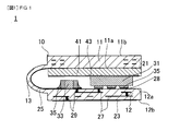
- Fig. 1 is a sectional view illustrating a reader/writer antenna module according to the present invention.
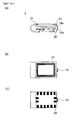
- Fig. 2 shows a top view and a sectional view illustrating the structure of the reader/writer antenna module according to the present invention before and after being folded.
- Fig. 2(A) is a top view of before folding.
- Fig. 2(B) is a sectional view of before folding.
- Fig. 2(C) is a sectional view of after folding.
- the reader/writer antenna module of this embodiment is structured as a HF-band reader/writer antenna module to be used in short-range communication with an RFID tag.
- a flexible substrate 10 includes a first base portion 11, a second base portion 12 and a bending portion 13 that connects the first base portion 11 and the second base portion 12 to each other.
- the flexible substrate 10 is formed of a flexible resin sheet that possesses flexibility and elasticity such a liquid crystal polymer or a polyimide, and the first base portion 11, the second base portion 12 and the bending portion 13 are integrally formed with each other by using this flexible resin sheet.
- a multilayer body formed by stacking a plurality of flexible resin sheets is formed in at least the first base portion 11 and the second base portion 12.
- the flexible substrate 10 is a multilayer body formed of identical flexible resin sheets, the substrate can be manufactured using a so-called sheet stacking process.
- the flexible substrate 10 can be manufactured using a simple process without using a complex process such as one in which the first base portion 11 and the second base portion 12 are manufactured and then connected to each other using the bending portion 13.
- a connection component such as a connector for connecting the first base portion 11 and the bending portion 13 and a connector for connecting the second base portion 12 and the bending portion 13
- impedance matching between an antenna conductor 21 and an RF circuit is simple.
- the rigidity of the first base portion 11 and the second base portion 12 depend on for example the thickness thereof, the density of wiring, the wiring material, the presence or absence of a magnetic layer and the presence or absence of a chip-type component. Therefore, the rigidity of the first base portion 11 and the second base portion 12 vary with thickness, wiring density and rigidity of wiring materials. In addition, the rigidity becomes relatively high with the presence of the magnetic layer 41 and chip-type components 31 and 33.
- the first base portion 11 of the flexible substrate 10 is provided with the antenna conductor 21, which is formed of a conductor pattern composed of for example a metal foil.
- the antenna conductor 21 is structured as a coil-shaped antenna conductor formed by stacking in a plurality of layers conductor patterns that loop through a plurality of turns and is provided on the outermost layer and in inner layers of the first base portion 11.
- the conductor patterns may be connected to one another through capacitive coupling or may be connected to one another through connection conductors formed of for example conductive paste.
- the magnetic layer 41 in which a magnetic powder such as ferrite is distributed in a resin material, is provided on a first main surface 11a of the first base portion 11.
- the magnetic layer 41 has larger outer dimensions than the antenna conductor 21.
- the magnetic layer 41 preferably has outer dimensions that are equal to or larger than those of the first base portion 11.
- the second base portion 12 of the flexible substrate 10 is provided with an RF circuit.
- This RF circuit is formed of the chip-type components 31 and 33 and wiring conductors 24 (refer to Fig. 2 ) for providing connections to the chip-type components 31 and 33.
- a wireless IC is illustrated as the chip-type component 31 and chip capacitors are illustrated as the chip-type components 33.
- the chip-type components 31 and 33 are mounted on the first main surface 12a of the second base portion 12 using surface conductors (lands) 28 and bonding material 35 such as solder.
- Examples of chip-type components include active components such as wireless ICs including memory circuits and logic circuits and liquid crystal oscillators, and passive components such as chip capacitors, chip inductors and chip resistors.
- inner conductors 27 and connection conductors 29 are provided in inner layers of the second base portion 12.
- the inner conductors 27 are provided on the surfaces of the flexible resin sheets.
- the connection conductors 29 are formed by forming through holes in the flexible resin sheets and filling the through holes with conductive paste.
- the inner conductors 27 and the connection conductors 29 are electrically connected to the surface conductors 28.
- the inner conductors 27 and the connection conductors 29 may be arranged in the inner layers of the second base portion so as to have a capacitance or an inductance in line with design values.
- connection conductor 25 for electrically connecting the antenna conductor 21 provided in the first base portion 11 and the RF circuit of the second base portion 12.
- the connection conductor 25 is formed of a flexible conductor material such as metal foil.
- the flexible substrate 10 has a structure that is folded utilizing the flexibility of the bending portion 13 such that the first main surface 11a of the first base portion 11 and the first main surface 12a of the second base portion 12 face each other (folded structure).
- the first main surface 11a of the first base portion and the first main surface 12a of the second base portion 12 form the same surface prior to being folded.
- the magnetic layer 41 is arranged between the antenna conductor 21 and the chip-type components 31 and 33.
- the magnetic layer 41 is present between the antenna conductor 21 and the chip-type components 31 and 33 (more specifically between the antenna conductor 21 and the RF circuit), it can be ensured that the antenna conductor 21 and the RF circuit are isolated from each other and the chip-type components 31 and 33 can be protected from external noise and external stress.
- the chip-type components 31 and 33 and the magnetic layer 41 are arranged between the first base portion 11 and the second base portion 12, a comparatively large curvature can be secured for the connection conductor 25 provided on the bending portion 13, and consequently the stress acting on the connection conductor 25 is small and reliability of conduction between the first base portion 11 and the second base portion 12 can be secured.
- a ground conductor 23 is provided on the second base portion 12 so as to substantially cover a region in which the RF circuit is formed in plan view.
- the ground conductor 23 is provided on the second main surface 12b of the second base portion 12.
- the chip-type components 31 and 33 on the second base portion 12 are arranged between the magnetic layer 41 and the ground conductor 23. Therefore, the RF circuit can be better isolated from external noise, the isolation characteristics of the RF circuit are improved and a reader/writer antenna module having high reliability can be formed.
- an adhesive layer 43 is provided on the surface of the magnetic layer 41, and the magnetic layer 41 and the chip-type component 31 are adhered to each other via the adhesive layer 43.
- the adhesive layer 43 is a sheet-shaped adhesive sheet such as double-sided tape. That is, a folded structure in which the first base portion 11 and the second base portion 12 face each other can be secured by using this adhesive sheet.
- This adhesive sheet adheres to the upper surface of the chip-type component 31, which has the greatest height among the chip-type components 31 and 33, and this greatest-height chip-type component 31 is mounted on a side of the second base portion 12 further away from the bending portion 13 side than a position in the center of the second base portion 12.
- a reader/writer antenna module can be formed in which the folded state of the first base portion 11 and the second base portion 12 is readily maintained and that is therefore excellent in terms of shape stability.
- connection conductor 25 on the bending portion 13 is provided so as to be positioned on the inner side of a folded structure. Consequently, a folded structure can be realized with which the risk of the connection conductor 25 being broken is small and that is excellent in terms of connection reliability.
- Solder resist patterns may be formed as needed on for example the connection conductor 25 and the ground conductor 23 provided on the outermost layers of the flexible substrate 10.
- the adhesive layer 43 is not limited to being a sheet-shaped adhesive sheet and may be instead formed of an adhesive for example.
- Fig. 3 shows an example of circuit diagrams used for the reader/writer antenna module according to the present invention.
- Fig. 3(A) is a block diagram.
- the reader/writer antenna module of this embodiment includes a reception circuit 73, a filter circuit 74 and a matching circuit 75 between a wireless IC 72 and an antenna 80.
- An RF circuit 70 is formed of an oscillator 71, the wireless IC 72, the reception circuit 73, the filter circuit 74 and the matching circuit 75.
- a transmission signal output from the wireless IC 72 is transmitted to the antenna 80 using a balanced path via the filter circuit 74 and the matching circuit 75.
- a reception signal received by the antenna 80 is transmitted to the wireless IC 72 using an unbalanced path via the matching circuit 75 and the reception circuit 73.
- the RF circuit 70 may be connected to another circuit, which is not illustrated, via for example a connector. As an example of connection to another circuit, for example, connection to a control circuit can be considered.
- Fig. 3(B) is an actual circuit diagram of the reception circuit 73, the filter circuit 74, the matching circuit 75 and the antenna 80.
- the filter circuit 74 and the matching circuit 75 share some capacitors.
- a transmission signal is transmitted to an antenna 80 via the filter circuit 74 and the matching circuit 75.
- a reception signal output from the matching circuit 75 is input to the reception circuit 73.
- the reception circuit 73 is a bias circuit for adjusting the direct current potential and amplitude of a reception signal.
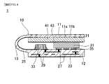
- Fig. 4 is a sectional view illustrating a reader/writer antenna module according to the present invention.
- the first base portion 11 may be formed of a single layer flexible resin sheet as in the reader/writer antenna module 1 of this embodiment.
- the antenna conductor 21 may be a two-layer coil-shaped antenna conductor formed on the front and back surfaces of the flexible resin sheet or may be a single-layer coil-shaped antenna provided on only the first main surface 11a (or the second main surface 11b) of the first base portion 11. This antenna is preferably formed in a plurality of turns, but may instead be formed in just one turn.
- the second base portion 12 may also be formed of a single-layer flexible resin sheet.
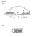
- Fig. 5 shows sectional views illustrating the structure of a reader/writer antenna module according to the present invention before and after being folded.
- Fig. 5(A) is a sectional view of before folding and
- Fig. 5(B) is a sectional view of after folding.
- the bending portion 13 may be connected to the first base portion 11 and the second base portion 12 at the side of surfaces opposite to the first main surfaces 11a and 12a (second main surfaces 11b and 12b), as in the reader/writer antenna module 1 of this embodiment. With this folded structure, the curvature of the connection conductor 25 can be made larger.
- the ground conductor 23 in the second base portion 12 may be provided in an inner layer of the second base portion 12.
- Fig. 6 is a sectional view illustrating a reader/writer antenna module according to the present invention.
- a chip-type component (in this embodiment, wireless IC) 37 may be built into the second base portion 12, as in the reader/writer antenna module 1 of this embodiment.
- the upper surfaces of chip-type components 34 which have the greatest height among the chip-type components 33 and 34 mounted on the first main surface 12a of the second base portion 12 can be used as surfaces to be adhered to the adhesion layer 43.
- the connection conductor 25 in the bending portion 13 may be provided between layers of flexible resin sheets.
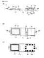
- Fig. 7 illustrates the structure of a reader/writer antenna module according to the present invention before being folded.
- Fig. 7(A) is a sectional view
- Fig. 7(B) is a top view
- Fig. 7(C) is a bottom view.
- Fig. 8 illustrates the structure after folding.
- Fig. 8(A) is a sectional view
- Fig. 8(B) is a top view
- Fig. 8(C) is a bottom view.
- the antenna conductor 21 is exposed on the second main surface 11b on the side of the first base portion 11 on which the magnetic layer 41 is not provided.
- the surface conductors 28 are formed on the second main surface 12b on the side of the second base portion 12 on which the chip-type components 31 and 33 are not mounted.
- the surface conductors 28 are electrically connected to the inner conductors 27 and interlayer conductors 29 within the second base portion 12. After folding, the antenna conductor 21 and the surface conductors 28 are exposed on the surfaces of the reader/writer antenna module.
- the surface conductors 28 are to be connected to for example a printed wiring board via a bonding material.
- the folded structure is maintained without using an adhesive sheet by engaging a hook portion 14a provided on the first base portion 11 and a hook portion 14b provided on the second base portion 12 with each other.
- a configuration may be adopted in which the hook portions 14a and 14b are engaged with each other in addition to using an adhesive sheet.
- the hook portions 14a and 14b can also be formed integrally with the first base portion 11, the second base portion 12 and the bending portion 13 using the same material.
- the folded structure is maintained by the hook portions 14a and 14b, it is possible to easily switch between the non-folded structure and the folded structure by unfastening the hook portions 14a and 14b.
- Fig. 9 illustrates the structure of a reader/writer antenna module according to the present invention before being folded.
- Fig. 9(A) is a sectional view
- Fig. 9(B) is a top view
- Fig. 9(C) is a bottom view.
- Fig. 10 illustrates the structure at the time of mounting.
- Fig. 10(A) is a sectional view
- Fig. 10(B) is a top view
- Fig. 10(C) is a bottom view.
- Fig. 11 illustrates the structure at the time of use.
- Fig. 11(A) is a sectional view
- Fig. 11(B) is a top view
- Fig. 11(C) is a bottom view.
- the first base portion 11 has a twice-folded structure. By adopting this structure, it is possible to increase the area of the opening formed by the antenna conductor 21 while retaining the small size of the second base portion 12.
- the first base portion 11 is folded and as a result has approximately the same dimensions as the second base portion 12, and the hook portions 14a and 14b are fastened together.
- an SMD type component can be formed. Accordingly, it is possible to tape this module in the same manner as a typical component.
- reflow mounting can also be performed.
- the first base portion 11 is expanded by unfastening the hook portions 14a and 14b. Then, in a state in which the first base portion 11 has been expanded, the magnetic layer 41 can be arranged between the antenna conductor 21 and the chip-type components 31 and 33 by fastening once again the hook portions 14a and 14b.
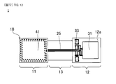
- Fig. 12 is a top view illustrating a reader/writer antenna module according to the present invention.
- the longitudinal direction of the chip-type components (in this embodiment, chip capacitors) 33 which are arranged on a side of the second base portion 12 closer to the bending portion 13 than a position in the center of the second base portion 12, be arranged so as to be parallel with a boundary line between the second base portion 12 and the bending portion 13.
- the chip-type components 33 can be prevented from falling off at the time of folding by arranging the chip-type components 33 in this manner.
- Fig. 13 illustrates an antenna device according to the present invention.
- Fig. 13(A) is a sectional view and
- Fig. 13(B) is a top view illustrating the positional relationship between a booster antenna and a reader/writer antenna module.
- Fig. 14 shows a perspective view and an equivalent circuit diagram of the booster antenna.
- the size of the antenna conductor of the reader/writer antenna modules described in Embodiments 1 to 7 is comparatively small. Consequently, in cases where it is necessary to secure a large communication range, it is preferable to add an antenna booster as illustrated in Fig. 13 .
- An antenna device 50 includes the reader/writer antenna module 1, a printed wiring board 53, a booster antenna 55, a base sheet 57, an adhesive layer 59 and a casing 51.
- the reader/writer antenna module 1 is mounted on a surface of the printed wiring board 53 via bonding material 61.
- a feeder circuit (not illustrated), which feeds electricity to the reader/writer antenna module, is formed on the printed wiring board 53.
- the printed wiring board 53 is housed inside the casing 51.
- the booster antenna 55 is formed as result of two coil patterns 55a and 55b formed on the two main surfaces of the flexible base sheet 57 being capacitively coupled with each other. As illustrated in Fig. 14(A) , the coil patterns 55a and 55b loop such that induced currents generated in the coil patterns 55a and 55b flow in the same direction. In addition, the booster antenna 55 and the base sheet 57 are fixed to an inner wall of the casing 51 with the adhesive layer 59.
- the booster antenna 55 as illustrated in Fig. 14(B) , is formed of an LC resonance circuit and has a resonant frequency that corresponds to the carrier frequency (13.56 MHz).
- the coil axis of the booster antenna 55 is arranged so as to be parallel with the coil axis of the antenna conductor 21 of the reader/writer antenna module 1.
- the outer dimensions of the booster antenna 55 are larger than those of the antenna conductor 21.
- the opening of the coil of the antenna conductor 21 is arranged so as to be positioned inside the opening of the coil of the booster antenna 55.
- the position of the antenna conductor 21 is arranged in the vicinity of the positions of the coil patterns 55a and 55b of the booster antenna 55 so that the antenna conductor 21 and the booster antenna 55 are coupled with each other via a magnetic field.
- the coil axis of the booster antenna 55 and the coil axis of the antenna conductor 21 may be arranged so as to be orthogonal to each other.
- a transmission signal generated by a wireless IC (not illustrated) is transmitted to the booster antenna 55 via the antenna conductor 21. Then, the transmission signal is transmitted to the antenna of a communication partner from the booster antenna 55. On the other hand, at the time of reception, a signal transmitted from the antenna of the communication partner is received by the booster antenna 55. Then, the reception signal is transmitted to the wireless IC via the antenna conductor 21.
- the antenna conductor 21 and the booster antenna 55 are coupled with each other via a magnetic field. Consequently, there is no need for the booster antenna 55 to be connected to a feeder circuit via contact pins or flexible cables.
- the antenna conductor 21 have a resonant frequency that corresponds to the carrier frequency.
- the resonant frequency of the booster antenna 55 varies after coupling depending on the degree of electromagnetic coupling between the booster antenna 55 and the antenna conductor 21. The degree of coupling is determined by design factors such as the distance between the antenna conductor 21 and the booster antenna 55 and the areas of the openings of the coils. Consequently, the resonant frequency of the antenna conductor 21 may be set so be equal to the carrier frequency (13.56 MHz) after coupling with the booster antenna 55.
- the antenna conductor 21 and the booster antenna 55 are coupled with each other via a magnetic field, but they may instead be coupled with each other via an electric field.
Landscapes
- Engineering & Computer Science (AREA)
- Physics & Mathematics (AREA)
- Electromagnetism (AREA)
- Health & Medical Sciences (AREA)
- Toxicology (AREA)
- General Health & Medical Sciences (AREA)
- Computer Networks & Wireless Communication (AREA)
- Artificial Intelligence (AREA)
- Computer Vision & Pattern Recognition (AREA)
- General Physics & Mathematics (AREA)
- Theoretical Computer Science (AREA)
- Details Of Aerials (AREA)
- Support Of Aerials (AREA)
- Structure Of Printed Boards (AREA)
Abstract
Description
- The present invention relates to reader/writer antenna modules, and in particular relates to HF-band reader/writer antenna modules used in short-range communication with radio frequency identification (RFID) tags and to antenna devices employing the HF-band reader/writer antenna modules.
- An RFID system in which communication is performed between a reader/writer and an RFID tag using a non-contact method so as to transmit information between the reader/writer and the RFID tag is an example of a known merchandise management system. The reader/writer includes a wireless IC for processing wireless signals and an antenna for transmitting and receiving wireless signals. Predetermined information is transmitted and received in the form of high-frequency signals via an electromagnetic field between an antenna of the RFID tag and an antenna of the reader/writer.
- In recent years, the field of use of RFID systems has been becoming wider and wider and there are applications in which a reader/writer is mounted in for example a mobile communication terminal. Consequently, reader/writers have been becoming increasing smaller in size and card-type reader/writer antenna modules have been proposed such as the one described in
Patent Document 1. This antenna module has a structure in which an antenna conductor, a semiconductor memory and so forth are integrated with flexible wiring substrates, and a substrate on which an antenna conductor has been provided and a substrate on which a chip-type component such as a semiconductor memory has been provided are stacked one on top of the other and the substrates are connected to each other with flexible lead wiring. - Patent Document 1: International Publication No.
WO 2007/105469 - In this structure, the substrate on which the antenna conductor is provided is stacked on a surface of the substrate, on which the chip-type component is provided, on the side opposite to the surface on which the chip-type component is provided. Consequently, the chip-type component is exposed on the surface and in order to protect the chip-type component from external noise and external stress, for example, a metal case or a resin layer needs to be separately provided. In addition, the substrate on which the antenna conductor is provided and the substrate on which the mounted component is provided are directly affixed to each other and therefore the curvature of the lead wiring connecting the substrates is small and sometimes the reliability of conduction between the substrates is not sufficiently secured due to the large bending stress acting on the lead wiring.
- The present invention has been made in light of the above-described problems.
- A reader/writer antenna module of the present invention employs a flexible substrate that includes a first base portion, a second base portion and a bending portion that connects the first base portion and the second base portion. The flexible substrate is mainly characterized by having a structure that is folded by utilizing the flexibility of the bending portion such that a first main surface of the first base portion and a first main surface of the second base portion face each other (hereafter, folded structure), and by there being a magnetic layer arranged between an antenna conductor and a chip-type component in this folded structure. Advantageous Effects of Invention
- In this invention, since a magnetic layer is interposed between the antenna conductor and the chip-type component (more specifically between the antenna conductor and an RF circuit including the chip-type component), it can be ensured that the antenna conductor and the chip-type component (more specifically, the RF circuit) are isolated from each other and the chip-type component can be protected from external noise and external stress. In addition, since the chip-type component and the magnetic layer are arranged between the first base portion and the second base portion, it is possible for a connection conductor to have a comparatively large curvature and consequently bending stress acting on the connection conductor is reduced and reliability of conduction between the substrates can be secured.
-
- [
Fig. 1] Fig. 1 is a sectional view illustrating a reader/writer antenna module according to the present invention. (Embodiment 1) - [
Fig. 2] Fig. 2 shows a top view and a sectional view illustrating the structure of the reader/writer antenna module according to the present invention before and after being folded. (Embodiment 1) - [
Fig. 3] Fig. 3 shows an example of circuit diagrams used for the reader/writer antenna module according to the present invention. (Embodiment 1) - [
Fig. 4] Fig. 4 is a sectional view illustrating a reader/writer antenna module according to the present invention. (Embodiment 2) - [
Fig. 5] Fig. 5 is a sectional view illustrating the structure of a reader/writer antenna module according to the present invention before and after being folded. (Embodiment 3) - [
Fig. 6] Fig. 6 is a sectional view illustrating a reader/writer antenna module according to the present invention. (Embodiment 4) - [
Fig. 7] Fig. 7 shows a sectional view, a top view and a bottom view illustrating the structure of a reader/writer antenna module according to the present invention before being folded. (Embodiment 5) - [
Fig. 8] Fig. 8 shows a sectional view, a top view and a bottom view illustrating the structure of the reader/writer antenna module according to the present invention after being folded. (Embodiment 5) - [
Fig. 9] Fig. 9 shows a sectional view, a top view and a bottom view illustrating the structure of a reader/writer antenna module according to the present invention before being folded. (Embodiment 6) - [
Fig. 10] Fig. 10 shows a sectional view, a top view and a bottom view illustrating the structure of the reader/writer antenna module according to the present invention at the time of mounting. (Embodiment 6) - [
Fig. 11] Fig. 11 shows a sectional view, a top view and a bottom view illustrating the structure of the reader/writer antenna module according to the present invention at the time of use. (Embodiment 6) - [
Fig. 12] Fig. 12 is a top view illustrating a reader/writer antenna module according to the present invention. (Embodiment 7) - [
Fig. 13] Fig. 13 shows a sectional view and a top view illustrating an antenna device according to the present invention. (Embodiment 8) - [
Fig. 14] Fig. 14 shows a perspective view and an equivalent circuit diagram illustrating a booster antenna. (Embodiment 8) - Hereafter, modes for carrying out the present invention will be described.
-
Fig. 1 is a sectional view illustrating a reader/writer antenna module according to the present invention. In addition,Fig. 2 shows a top view and a sectional view illustrating the structure of the reader/writer antenna module according to the present invention before and after being folded.Fig. 2(A) is a top view of before folding. In addition,Fig. 2(B) is a sectional view of before folding. In addition,Fig. 2(C) is a sectional view of after folding. The reader/writer antenna module of this embodiment is structured as a HF-band reader/writer antenna module to be used in short-range communication with an RFID tag. - A
flexible substrate 10 includes afirst base portion 11, asecond base portion 12 and abending portion 13 that connects thefirst base portion 11 and thesecond base portion 12 to each other. Theflexible substrate 10 is formed of a flexible resin sheet that possesses flexibility and elasticity such a liquid crystal polymer or a polyimide, and thefirst base portion 11, thesecond base portion 12 and thebending portion 13 are integrally formed with each other by using this flexible resin sheet. In addition, a multilayer body formed by stacking a plurality of flexible resin sheets is formed in at least thefirst base portion 11 and thesecond base portion 12. Thus, since theflexible substrate 10 is a multilayer body formed of identical flexible resin sheets, the substrate can be manufactured using a so-called sheet stacking process. For example, theflexible substrate 10 can be manufactured using a simple process without using a complex process such as one in which thefirst base portion 11 and thesecond base portion 12 are manufactured and then connected to each other using the bendingportion 13. In addition, since there is no need for a connection component such as a connector for connecting thefirst base portion 11 and the bendingportion 13 and a connector for connecting thesecond base portion 12 and the bendingportion 13, in particular, impedance matching between anantenna conductor 21 and an RF circuit is simple. The rigidity of thefirst base portion 11 and thesecond base portion 12 depend on for example the thickness thereof, the density of wiring, the wiring material, the presence or absence of a magnetic layer and the presence or absence of a chip-type component. Therefore, the rigidity of thefirst base portion 11 and thesecond base portion 12 vary with thickness, wiring density and rigidity of wiring materials. In addition, the rigidity becomes relatively high with the presence of themagnetic layer 41 and chip-type components - The
first base portion 11 of theflexible substrate 10 is provided with theantenna conductor 21, which is formed of a conductor pattern composed of for example a metal foil. Theantenna conductor 21 is structured as a coil-shaped antenna conductor formed by stacking in a plurality of layers conductor patterns that loop through a plurality of turns and is provided on the outermost layer and in inner layers of thefirst base portion 11. The conductor patterns may be connected to one another through capacitive coupling or may be connected to one another through connection conductors formed of for example conductive paste. - In addition, the
magnetic layer 41, in which a magnetic powder such as ferrite is distributed in a resin material, is provided on a firstmain surface 11a of thefirst base portion 11. Themagnetic layer 41 has larger outer dimensions than theantenna conductor 21. Themagnetic layer 41 preferably has outer dimensions that are equal to or larger than those of thefirst base portion 11. - The
second base portion 12 of theflexible substrate 10 is provided with an RF circuit. This RF circuit is formed of the chip-type components Fig. 2 ) for providing connections to the chip-type components type component 31 and chip capacitors are illustrated as the chip-type components 33. The chip-type components main surface 12a of thesecond base portion 12 using surface conductors (lands) 28 andbonding material 35 such as solder. Examples of chip-type components include active components such as wireless ICs including memory circuits and logic circuits and liquid crystal oscillators, and passive components such as chip capacitors, chip inductors and chip resistors. - In addition,
inner conductors 27 andconnection conductors 29 are provided in inner layers of thesecond base portion 12. Theinner conductors 27 are provided on the surfaces of the flexible resin sheets. In addition, theconnection conductors 29 are formed by forming through holes in the flexible resin sheets and filling the through holes with conductive paste. Theinner conductors 27 and theconnection conductors 29 are electrically connected to thesurface conductors 28. Theinner conductors 27 and theconnection conductors 29 may be arranged in the inner layers of the second base portion so as to have a capacitance or an inductance in line with design values. - The bending
portion 13 of theflexible substrate 10 is provided with aconnection conductor 25 for electrically connecting theantenna conductor 21 provided in thefirst base portion 11 and the RF circuit of thesecond base portion 12. Theconnection conductor 25 is formed of a flexible conductor material such as metal foil. - In the reader/
writer antenna module 1 of this embodiment, theflexible substrate 10 has a structure that is folded utilizing the flexibility of the bendingportion 13 such that the firstmain surface 11a of thefirst base portion 11 and the firstmain surface 12a of thesecond base portion 12 face each other (folded structure). The firstmain surface 11a of the first base portion and the firstmain surface 12a of thesecond base portion 12 form the same surface prior to being folded. Themagnetic layer 41 is arranged between theantenna conductor 21 and the chip-type components magnetic layer 41 is present between theantenna conductor 21 and the chip-type components 31 and 33 (more specifically between theantenna conductor 21 and the RF circuit), it can be ensured that theantenna conductor 21 and the RF circuit are isolated from each other and the chip-type components type components magnetic layer 41 are arranged between thefirst base portion 11 and thesecond base portion 12, a comparatively large curvature can be secured for theconnection conductor 25 provided on the bendingportion 13, and consequently the stress acting on theconnection conductor 25 is small and reliability of conduction between thefirst base portion 11 and thesecond base portion 12 can be secured. - In this embodiment, a
ground conductor 23 is provided on thesecond base portion 12 so as to substantially cover a region in which the RF circuit is formed in plan view. In this embodiment, theground conductor 23 is provided on the secondmain surface 12b of thesecond base portion 12. The chip-type components second base portion 12 are arranged between themagnetic layer 41 and theground conductor 23. Therefore, the RF circuit can be better isolated from external noise, the isolation characteristics of the RF circuit are improved and a reader/writer antenna module having high reliability can be formed. - In addition, in the reader/
writer antenna module 1 of this embodiment, anadhesive layer 43 is provided on the surface of themagnetic layer 41, and themagnetic layer 41 and the chip-type component 31 are adhered to each other via theadhesive layer 43. In this embodiment, theadhesive layer 43 is a sheet-shaped adhesive sheet such as double-sided tape. That is, a folded structure in which thefirst base portion 11 and thesecond base portion 12 face each other can be secured by using this adhesive sheet. This adhesive sheet adheres to the upper surface of the chip-type component 31, which has the greatest height among the chip-type components type component 31 is mounted on a side of thesecond base portion 12 further away from the bendingportion 13 side than a position in the center of thesecond base portion 12. Thus, a reader/writer antenna module can be formed in which the folded state of thefirst base portion 11 and thesecond base portion 12 is readily maintained and that is therefore excellent in terms of shape stability. - In addition, in this embodiment, in the folded structure, the
connection conductor 25 on the bendingportion 13 is provided so as to be positioned on the inner side of a folded structure. Consequently, a folded structure can be realized with which the risk of theconnection conductor 25 being broken is small and that is excellent in terms of connection reliability. - Solder resist patterns may be formed as needed on for example the
connection conductor 25 and theground conductor 23 provided on the outermost layers of theflexible substrate 10. In addition, theadhesive layer 43 is not limited to being a sheet-shaped adhesive sheet and may be instead formed of an adhesive for example. -
Fig. 3 shows an example of circuit diagrams used for the reader/writer antenna module according to the present invention.Fig. 3(A) is a block diagram. The reader/writer antenna module of this embodiment includes areception circuit 73, afilter circuit 74 and amatching circuit 75 between awireless IC 72 and anantenna 80. AnRF circuit 70 is formed of anoscillator 71, thewireless IC 72, thereception circuit 73, thefilter circuit 74 and thematching circuit 75. A transmission signal output from thewireless IC 72 is transmitted to theantenna 80 using a balanced path via thefilter circuit 74 and thematching circuit 75. On the other hand, a reception signal received by theantenna 80 is transmitted to thewireless IC 72 using an unbalanced path via thematching circuit 75 and thereception circuit 73. TheRF circuit 70 may be connected to another circuit, which is not illustrated, via for example a connector. As an example of connection to another circuit, for example, connection to a control circuit can be considered. -
Fig. 3(B) is an actual circuit diagram of thereception circuit 73, thefilter circuit 74, the matchingcircuit 75 and theantenna 80. - The
filter circuit 74 and thematching circuit 75 share some capacitors. A transmission signal is transmitted to anantenna 80 via thefilter circuit 74 and thematching circuit 75. In addition, a reception signal output from the matchingcircuit 75 is input to thereception circuit 73.
Thereception circuit 73 is a bias circuit for adjusting the direct current potential and amplitude of a reception signal. -
Fig. 4 is a sectional view illustrating a reader/writer antenna module according to the present invention. - The
first base portion 11 may be formed of a single layer flexible resin sheet as in the reader/writer antenna module 1 of this embodiment. In this case, as illustrated, theantenna conductor 21 may be a two-layer coil-shaped antenna conductor formed on the front and back surfaces of the flexible resin sheet or may be a single-layer coil-shaped antenna provided on only the firstmain surface 11a (or the secondmain surface 11b) of thefirst base portion 11. This antenna is preferably formed in a plurality of turns, but may instead be formed in just one turn. Thesecond base portion 12 may also be formed of a single-layer flexible resin sheet. -
Fig. 5 shows sectional views illustrating the structure of a reader/writer antenna module according to the present invention before and after being folded.Fig. 5(A) is a sectional view of before folding andFig. 5(B) is a sectional view of after folding. - The bending
portion 13 may be connected to thefirst base portion 11 and thesecond base portion 12 at the side of surfaces opposite to the firstmain surfaces main surfaces writer antenna module 1 of this embodiment. With this folded structure, the curvature of theconnection conductor 25 can be made larger. In addition, theground conductor 23 in thesecond base portion 12 may be provided in an inner layer of thesecond base portion 12. -
Fig. 6 is a sectional view illustrating a reader/writer antenna module according to the present invention. A chip-type component (in this embodiment, wireless IC) 37 may be built into thesecond base portion 12, as in the reader/writer antenna module 1 of this embodiment. In this case, the upper surfaces of chip-type components 34, which have the greatest height among the chip-type components main surface 12a of thesecond base portion 12 can be used as surfaces to be adhered to theadhesion layer 43. In addition, theconnection conductor 25 in the bendingportion 13 may be provided between layers of flexible resin sheets. -
Fig. 7 illustrates the structure of a reader/writer antenna module according to the present invention before being folded.Fig. 7(A) is a sectional view,Fig. 7(B) is a top view andFig. 7(C) is a bottom view. In addition,Fig. 8 illustrates the structure after folding.Fig. 8(A) is a sectional view,Fig. 8(B) is a top view andFig. 8(C) is a bottom view. - The
antenna conductor 21 is exposed on the secondmain surface 11b on the side of thefirst base portion 11 on which themagnetic layer 41 is not provided. In addition, thesurface conductors 28 are formed on the secondmain surface 12b on the side of thesecond base portion 12 on which the chip-type components surface conductors 28 are electrically connected to theinner conductors 27 andinterlayer conductors 29 within thesecond base portion 12. After folding, theantenna conductor 21 and thesurface conductors 28 are exposed on the surfaces of the reader/writer antenna module. Thesurface conductors 28 are to be connected to for example a printed wiring board via a bonding material. - In addition, the folded structure is maintained without using an adhesive sheet by engaging a
hook portion 14a provided on thefirst base portion 11 and ahook portion 14b provided on thesecond base portion 12 with each other. Alternatively, a configuration may be adopted in which thehook portions - The
hook portions first base portion 11, thesecond base portion 12 and the bendingportion 13 using the same material. In addition, since the folded structure is maintained by thehook portions hook portions -
Fig. 9 illustrates the structure of a reader/writer antenna module according to the present invention before being folded.Fig. 9(A) is a sectional view,Fig. 9(B) is a top view andFig. 9(C) is a bottom view. In addition,Fig. 10 illustrates the structure at the time of mounting.Fig. 10(A) is a sectional view,Fig. 10(B) is a top view andFig. 10(C) is a bottom view. In addition,Fig. 11 illustrates the structure at the time of use.Fig. 11(A) is a sectional view,Fig. 11(B) is a top view andFig. 11(C) is a bottom view. - In this embodiment, the
first base portion 11 has a twice-folded structure. By adopting this structure, it is possible to increase the area of the opening formed by theantenna conductor 21 while retaining the small size of thesecond base portion 12. - At the time of supply of and the time of mounting of the reader/writer antenna module, as illustrated in
Fig. 10 , thefirst base portion 11 is folded and as a result has approximately the same dimensions as thesecond base portion 12, and thehook portions - At the time of use of the reader/writer antenna module, as illustrated in
Fig. 11 , thefirst base portion 11 is expanded by unfastening thehook portions first base portion 11 has been expanded, themagnetic layer 41 can be arranged between theantenna conductor 21 and the chip-type components hook portions -
Fig. 12 is a top view illustrating a reader/writer antenna module according to the present invention. In the reader/writer antenna module 1 of this embodiment, among the chip-type components main surface 12a of thesecond base portion 12, it is preferable that the longitudinal direction of the chip-type components (in this embodiment, chip capacitors) 33, which are arranged on a side of thesecond base portion 12 closer to the bendingportion 13 than a position in the center of thesecond base portion 12, be arranged so as to be parallel with a boundary line between thesecond base portion 12 and the bendingportion 13. Since a greater bending stress acts on the side of thesecond base portion 12 closer to the bendingportion 13 than a position in the center of thesecond base portion 12 when the bendingportion 13 is folded, the chip-type components 33 can be prevented from falling off at the time of folding by arranging the chip-type components 33 in this manner. -
Fig. 13 illustrates an antenna device according to the present invention.Fig. 13(A) is a sectional view andFig. 13(B) is a top view illustrating the positional relationship between a booster antenna and a reader/writer antenna module. In addition,Fig. 14 shows a perspective view and an equivalent circuit diagram of the booster antenna. - The size of the antenna conductor of the reader/writer antenna modules described in
Embodiments 1 to 7 is comparatively small. Consequently, in cases where it is necessary to secure a large communication range, it is preferable to add an antenna booster as illustrated inFig. 13 . - An
antenna device 50 includes the reader/writer antenna module 1, a printedwiring board 53, abooster antenna 55, abase sheet 57, anadhesive layer 59 and acasing 51. - The reader/
writer antenna module 1 is mounted on a surface of the printedwiring board 53 viabonding material 61. In addition, a feeder circuit (not illustrated), which feeds electricity to the reader/writer antenna module, is formed on the printedwiring board 53. The printedwiring board 53 is housed inside thecasing 51. - The
booster antenna 55 is formed as result of twocoil patterns flexible base sheet 57 being capacitively coupled with each other. As illustrated inFig. 14(A) , thecoil patterns coil patterns booster antenna 55 and thebase sheet 57 are fixed to an inner wall of thecasing 51 with theadhesive layer 59. - The
booster antenna 55, as illustrated inFig. 14(B) , is formed of an LC resonance circuit and has a resonant frequency that corresponds to the carrier frequency (13.56 MHz). - In this embodiment, the coil axis of the
booster antenna 55 is arranged so as to be parallel with the coil axis of theantenna conductor 21 of the reader/writer antenna module 1. The outer dimensions of thebooster antenna 55 are larger than those of theantenna conductor 21. In addition, the opening of the coil of theantenna conductor 21 is arranged so as to be positioned inside the opening of the coil of thebooster antenna 55. In particular, the position of theantenna conductor 21 is arranged in the vicinity of the positions of thecoil patterns booster antenna 55 so that theantenna conductor 21 and thebooster antenna 55 are coupled with each other via a magnetic field. The coil axis of thebooster antenna 55 and the coil axis of theantenna conductor 21 may be arranged so as to be orthogonal to each other. - At the time of transmission, a transmission signal generated by a wireless IC (not illustrated) is transmitted to the
booster antenna 55 via theantenna conductor 21. Then, the transmission signal is transmitted to the antenna of a communication partner from thebooster antenna 55. On the other hand, at the time of reception, a signal transmitted from the antenna of the communication partner is received by thebooster antenna 55. Then, the reception signal is transmitted to the wireless IC via theantenna conductor 21. - Thus, the
antenna conductor 21 and thebooster antenna 55 are coupled with each other via a magnetic field. Consequently, there is no need for thebooster antenna 55 to be connected to a feeder circuit via contact pins or flexible cables. - In order to improve the transmission efficiency of a high-frequency signal, it is preferable that the
antenna conductor 21 have a resonant frequency that corresponds to the carrier frequency. Sometimes the resonant frequency of thebooster antenna 55 varies after coupling depending on the degree of electromagnetic coupling between thebooster antenna 55 and theantenna conductor 21. The degree of coupling is determined by design factors such as the distance between theantenna conductor 21 and thebooster antenna 55 and the areas of the openings of the coils. Consequently, the resonant frequency of theantenna conductor 21 may be set so be equal to the carrier frequency (13.56 MHz) after coupling with thebooster antenna 55. - In this embodiment, a case was described in which the
antenna conductor 21 and thebooster antenna 55 are coupled with each other via a magnetic field, but they may instead be coupled with each other via an electric field. -
- 1 reader/writer antenna module
- 10 flexible substrate
- 11 first base portion
- 11a first main surface
- 11b second main surface
- 12 second base portion
- 12a first main surface
- 12b second main surface
- 13 bending portion
- 14a, 14b hook portion
- 21 antenna conductor
- 23 ground conductor
- 24 wiring conductor
- 25 connection conductor
- 27 inner conductor
- 28 surface conductor
- 29 interlayer conductor
- 31 chip-type component (wireless IC)
- 33 chip-type component (chip capacitor)
- 34 chip-type component (chip capacitor)
- 35 bonding material
- 37 chip-type component (wireless IC)
- 41 magnetic layer
- 43 adhesive layer
- 50 antenna device
- 51 casing
- 53 printed wiring board
- 55 booster antenna
- 55a, 55b coil pattern
- 57 base sheet
- 59 adhesive layer
- 61 bonding material
- 70 RF circuit
- 71 oscillator
- 72 wireless IC
- 73 reception circuit
- 74 filter circuit
- 75 matching circuit
- 80 antenna
Claims (10)
- A reader/writer antenna module comprising
a flexible substrate including a first base portion, a second base portion and a bending portion that connects the first base portion and the second base portion to each other,
an antenna conductor provided to the first base portion,
a chip-type component that is mounted on a first main surface of the second base portion and is included in an RF circuit,
a flexible connection conductor that is provided to the bending portion and is for electrically connecting the antenna conductor and the chip-type component to each other, and
a magnetic layer that is provided on a first main surface of the first base portion,
wherein the flexible substrate has a folded structure that is folded such that the first main surface of the first base portion and the first main surface of the second base portion face each other, and
wherein the magnetic layer is arranged between the antenna conductor and the chip-type component. - The reader/writer antenna module according to Claim 1, wherein the second base portion is provided with a ground conductor and the chip-type component is arranged between the magnetic layer and the ground conductor.
- The reader/writer antenna module according to Claim 1 or 2, wherein an adhesive layer is provided on a surface of the magnetic layer and the magnetic layer and the chip-type component are adhered to each other via the adhesive layer, and thereby the folded structure is maintained.
- The reader/writer antenna module according to Claim 3, wherein the adhesion layer is formed of a sheet-shaped adhesive sheet and the adhesive sheet is adhered to an upper surface of a chip-type component having the greatest height among chip-type components.
- The reader/writer antenna module according to Claim 4, wherein the component having the greatest height among the chip-type components is mounted on a side of the second base portion that is further away from the bending portion than a position in the center of the second base portion.
- The reader/writer antenna module according to any one of Claims 1 to 5, wherein the flexible substrate is formed of a flexible resin sheet, and the first base portion, the second base portion and the bending portion are integrally formed using the flexible resin sheet.
- The reader/writer antenna module according to Claim 6 wherein, in at least the first base portion and the second base portion, the flexible substrate is formed of a multilayer body in which a plurality of the flexible resin sheets are stacked on top of one another.
- The reader/writer antenna module according to Claim 6 or 7, wherein the connection conductor is provided so as to be arranged on an inner side of the flexible resin sheet in the folded structure.
- The reader/writer antenna module according to any one of Claims 1 to 8, wherein, among the chip-type components, the longitudinal direction of a chip-type component arranged on a side of the second base portion that is closer to the bending portion than a position in the center of the second base portion, is arranged so as to be parallel with a boundary line between the second base portion and the bending portion.
- An antenna device comprising
the reader/writer antenna module according to any one of Claims 1 to 9,
a printed wiring board on a surface of which the reader/writer antenna module is mounted,
a booster antenna that is provided so as to be coupled with the antenna conductor of the reader/writer antenna module via an electromagnetic field and that has outer dimensions that are larger than those of the antenna conductor, and
a casing that houses inside thereof the printed wiring board and the booster antenna.
Applications Claiming Priority (2)
| Application Number | Priority Date | Filing Date | Title |
|---|---|---|---|
| JP2010205454 | 2010-09-14 | ||
| PCT/JP2011/070776 WO2012036139A1 (en) | 2010-09-14 | 2011-09-13 | Reader/writer antenna module and antenna device |
Publications (3)
| Publication Number | Publication Date |
|---|---|
| EP2618426A1 true EP2618426A1 (en) | 2013-07-24 |
| EP2618426A4 EP2618426A4 (en) | 2014-12-24 |
| EP2618426B1 EP2618426B1 (en) | 2019-05-08 |
Family
ID=45831598
Family Applications (1)
| Application Number | Title | Priority Date | Filing Date |
|---|---|---|---|
| EP11825141.2A Not-in-force EP2618426B1 (en) | 2010-09-14 | 2011-09-13 | Reader/writer antenna module and antenna device |
Country Status (5)
| Country | Link |
|---|---|
| US (1) | US8851390B2 (en) |
| EP (1) | EP2618426B1 (en) |
| JP (1) | JP5545371B2 (en) |
| CN (1) | CN103026551B (en) |
| WO (1) | WO2012036139A1 (en) |
Families Citing this family (49)
| Publication number | Priority date | Publication date | Assignee | Title |
|---|---|---|---|---|
| US9136600B2 (en) * | 2010-09-30 | 2015-09-15 | Murata Manufacturing Co., Ltd. | Antenna |
| CN103367889B (en) * | 2012-04-10 | 2018-02-02 | 上海曜传信息科技有限公司 | A kind of production technology of label antenna |
| US8950683B2 (en) | 2011-11-25 | 2015-02-10 | Zhijia Liu | Production process of tag antenna |
| US9935691B2 (en) * | 2013-12-19 | 2018-04-03 | Intel Corporation | Antenna configuration for dynamic re-distribution of magnetic fields |
| CN103683431B (en) * | 2013-12-26 | 2016-06-15 | 深圳佰维存储科技有限公司 | Integrated packaging wireless charging device |
| CN205902188U (en) * | 2014-03-27 | 2017-01-18 | 株式会社村田制作所 | Electrical components and mobile devices |
| JP6236367B2 (en) * | 2014-08-11 | 2017-11-22 | アルプス電気株式会社 | Sensor module and method of manufacturing sensor module |
| US20160169739A1 (en) * | 2014-12-03 | 2016-06-16 | Canon Kabushiki Kaisha | Electromagnetic wave detecting/generating device |
| US10725150B2 (en) | 2014-12-23 | 2020-07-28 | Infineon Technologies Ag | System and method for radar |
| US10317512B2 (en) * | 2014-12-23 | 2019-06-11 | Infineon Technologies Ag | RF system with an RFIC and antenna system |
| CN207459190U (en) * | 2015-01-15 | 2018-06-05 | 株式会社村田制作所 | Antenna device |
| JP2017011244A (en) * | 2015-06-26 | 2017-01-12 | アルプス電気株式会社 | Communication module and communication module manufacturing method |
| WO2017018134A1 (en) | 2015-07-30 | 2017-02-02 | 株式会社村田製作所 | Multilayer substrate and electronic device |
| JP2017038350A (en) * | 2015-08-07 | 2017-02-16 | デクセリアルズ株式会社 | Antenna device, electronic apparatus, mounting method of antenna device |
| CN207896252U (en) * | 2015-09-25 | 2018-09-21 | 株式会社村田制作所 | Anneta module and electronic equipment |
| EP3168789A1 (en) * | 2015-11-16 | 2017-05-17 | Gemalto Sa | Method for producing conductive tracks on a support |
| JP6610769B2 (en) * | 2016-03-02 | 2019-11-27 | 株式会社村田製作所 | Electronic component module, DC-DC converter, and electronic device |
| JP6380719B2 (en) * | 2016-06-30 | 2018-08-29 | 株式会社村田製作所 | Attachment type booster antenna and reader / writer using the same |
| CN109075822B (en) * | 2016-07-28 | 2021-08-10 | 株式会社村田制作所 | Wireless module, RFID system, and wireless power supply device |
| US10186779B2 (en) * | 2016-11-10 | 2019-01-22 | Advanced Semiconductor Engineering, Inc. | Semiconductor device package and method of manufacturing the same |
| JP2018105976A (en) * | 2016-12-26 | 2018-07-05 | 株式会社ジャパンディスプレイ | Display device |
| JP6562182B2 (en) * | 2017-03-13 | 2019-08-21 | 株式会社村田製作所 | Communication equipment |
| JP6239176B1 (en) * | 2017-04-21 | 2017-11-29 | 株式会社Maruwa | Antenna module |
| CN106934314A (en) * | 2017-04-25 | 2017-07-07 | 成都优孚达信息技术有限公司 | A kind of portable RFID and IC-card intelligent read-write device |
| JP6642764B2 (en) * | 2017-05-19 | 2020-02-12 | 株式会社村田製作所 | Electronic and communication equipment |
| WO2019009062A1 (en) | 2017-07-07 | 2019-01-10 | 株式会社村田製作所 | High frequency power circuit module |
| US10826193B2 (en) * | 2017-07-28 | 2020-11-03 | Samsung Electro-Mechanics Co., Ltd. | Antenna module including a flexible substrate |
| US10775490B2 (en) * | 2017-10-12 | 2020-09-15 | Infineon Technologies Ag | Radio frequency systems integrated with displays and methods of formation thereof |
| CN111433976A (en) * | 2017-12-14 | 2020-07-17 | 株式会社村田制作所 | Antenna devices, antenna modules and wireless devices |
| FR3075484B1 (en) * | 2017-12-18 | 2021-10-15 | Sagemcom Broadband Sas | ANTENNA FOR PRINTED CIRCUIT, ELECTRONIC CIRCUIT AND ELECTRONIC EQUIPMENT PROVIDED WITH SUCH ANTENNA |
| WO2019131581A1 (en) * | 2017-12-26 | 2019-07-04 | 株式会社村田製作所 | Inductor bridge and electronic apparatus |
| US11088468B2 (en) * | 2017-12-28 | 2021-08-10 | Samsung Electro-Mechanics Co., Ltd. | Antenna module |
| KR101940798B1 (en) * | 2018-03-06 | 2019-01-21 | 동우 화인켐 주식회사 | Film antenna and display device including the same |
| KR102066903B1 (en) | 2018-07-03 | 2020-01-16 | 삼성전자주식회사 | Antenna module |
| KR102059815B1 (en) | 2018-07-09 | 2019-12-27 | 삼성전기주식회사 | Antenna substrate and antenna module comprising the same |
| KR102089285B1 (en) | 2018-07-17 | 2020-03-16 | 삼성전자주식회사 | Antenna module |
| KR101934676B1 (en) * | 2018-07-24 | 2019-01-03 | 주식회사 기가레인 | Transmission line having improved bending durability |
| WO2020031776A1 (en) * | 2018-08-06 | 2020-02-13 | 株式会社村田製作所 | Antenna module |
| KR102137093B1 (en) | 2019-08-05 | 2020-07-23 | 삼성전기주식회사 | Antenna module and electronic device including thereof |
| KR102387748B1 (en) * | 2019-08-05 | 2022-04-15 | 삼성전기주식회사 | Antenna module and electronic device including thereof |
| DE102020203970A1 (en) * | 2020-03-26 | 2021-09-30 | Fraunhofer-Gesellschaft zur Förderung der angewandten Forschung eingetragener Verein | High-frequency arrangement with a front and a rear antenna |
| KR20220065551A (en) * | 2020-11-13 | 2022-05-20 | 삼성전기주식회사 | Package structure |
| KR102755830B1 (en) * | 2020-11-17 | 2025-01-20 | 동우 화인켐 주식회사 | Antenna package and image display device including the same |
| KR102400030B1 (en) | 2020-11-18 | 2022-05-18 | 동우 화인켐 주식회사 | Antenna package and image display device including the same |
| JP2022159893A (en) * | 2021-04-05 | 2022-10-18 | 日本電産モビリティ株式会社 | Communication device |
| US11916311B2 (en) * | 2021-04-30 | 2024-02-27 | Apple Inc. | Electronic devices having folded antenna modules |
| US11811957B2 (en) | 2021-05-19 | 2023-11-07 | Advanced Semiconductor Engineering, Inc. | Semiconductor device package and method of manufacturing the same |
| CN114335987B (en) * | 2022-03-15 | 2022-06-07 | 英内物联网科技启东有限公司 | Antenna module with RFID electronic tag formula |
| TWI815480B (en) * | 2022-05-25 | 2023-09-11 | 泓博無線通訊技術有限公司 | Ultra-wideband antenna module |
Family Cites Families (10)
| Publication number | Priority date | Publication date | Assignee | Title |
|---|---|---|---|---|
| JP2758099B2 (en) * | 1992-02-27 | 1998-05-25 | シャープ株式会社 | Multi-layer flexible printed wiring board |
| JPH07335443A (en) * | 1994-06-13 | 1995-12-22 | Hitachi Maxell Ltd | Coil device and IC memory device using the same |
| JP4190696B2 (en) * | 2000-03-02 | 2008-12-03 | 大日本印刷株式会社 | Antenna sheet and non-contact data carrier |
| JP3772778B2 (en) * | 2001-03-30 | 2006-05-10 | 三菱マテリアル株式会社 | Antenna coil, identification tag using the same, reader / writer device, reader device and writer device |
| JP3803085B2 (en) * | 2002-08-08 | 2006-08-02 | 株式会社日立製作所 | Wireless IC tag |
| WO2007015353A1 (en) * | 2005-08-03 | 2007-02-08 | Matsushita Electric Industrial Co., Ltd. | Storage medium with built-in antenna |
| US7775446B2 (en) | 2006-03-10 | 2010-08-17 | Panasonic Corporation | Card type information device and method for manufacturing same |
| JP5016252B2 (en) * | 2006-04-14 | 2012-09-05 | 株式会社タムラ製作所 | Connector integrated RFID reader / writer |
| JP2008040904A (en) | 2006-08-08 | 2008-02-21 | Hitachi Ltd | RFID tag and reading method thereof |
| JP5488593B2 (en) | 2009-05-14 | 2014-05-14 | 株式会社村田製作所 | Circuit board and circuit module |
-
2011
- 2011-09-13 WO PCT/JP2011/070776 patent/WO2012036139A1/en not_active Ceased
- 2011-09-13 EP EP11825141.2A patent/EP2618426B1/en not_active Not-in-force
- 2011-09-13 CN CN201180035924.XA patent/CN103026551B/en not_active Expired - Fee Related
- 2011-09-13 JP JP2012534005A patent/JP5545371B2/en not_active Expired - Fee Related
-
2012
- 2012-12-31 US US13/731,207 patent/US8851390B2/en not_active Expired - Fee Related
Also Published As
| Publication number | Publication date |
|---|---|
| JP5545371B2 (en) | 2014-07-09 |
| CN103026551A (en) | 2013-04-03 |
| WO2012036139A1 (en) | 2012-03-22 |
| US20130112754A1 (en) | 2013-05-09 |
| JPWO2012036139A1 (en) | 2014-02-03 |
| CN103026551B (en) | 2015-03-25 |
| EP2618426A4 (en) | 2014-12-24 |
| US8851390B2 (en) | 2014-10-07 |
| EP2618426B1 (en) | 2019-05-08 |
Similar Documents
| Publication | Publication Date | Title |
|---|---|---|
| US8851390B2 (en) | Reader/writer antenna module and antenna device | |
| US9812764B2 (en) | Antenna device and wireless device | |
| US10396429B2 (en) | Wireless communication device | |
| US8757502B2 (en) | Wireless communication device | |
| CN103370834B (en) | Wireless communication devices | |
| US9865913B2 (en) | Communication terminal and card antenna module | |
| US9336475B2 (en) | Radio IC device and radio communication terminal |
Legal Events
| Date | Code | Title | Description |
|---|---|---|---|
| PUAI | Public reference made under article 153(3) epc to a published international application that has entered the european phase |
Free format text: ORIGINAL CODE: 0009012 |
|
| 17P | Request for examination filed |
Effective date: 20130212 |
|
| AK | Designated contracting states |
Kind code of ref document: A1 Designated state(s): AL AT BE BG CH CY CZ DE DK EE ES FI FR GB GR HR HU IE IS IT LI LT LU LV MC MK MT NL NO PL PT RO RS SE SI SK SM TR |
|
| DAX | Request for extension of the european patent (deleted) | ||
| RIC1 | Information provided on ipc code assigned before grant |
Ipc: H01Q 1/22 20060101ALI20141112BHEP Ipc: H01Q 1/40 20060101ALI20141112BHEP Ipc: H01Q 1/38 20060101ALI20141112BHEP Ipc: H01Q 1/20 20060101ALI20141112BHEP Ipc: G06K 7/10 20060101ALI20141112BHEP Ipc: H01Q 7/00 20060101AFI20141112BHEP Ipc: H01Q 1/52 20060101ALI20141112BHEP |
|
| A4 | Supplementary search report drawn up and despatched |
Effective date: 20141120 |
|
| STAA | Information on the status of an ep patent application or granted ep patent |
Free format text: STATUS: EXAMINATION IS IN PROGRESS |
|
| 17Q | First examination report despatched |
Effective date: 20170322 |
|
| GRAP | Despatch of communication of intention to grant a patent |
Free format text: ORIGINAL CODE: EPIDOSNIGR1 |
|
| STAA | Information on the status of an ep patent application or granted ep patent |
Free format text: STATUS: GRANT OF PATENT IS INTENDED |
|
| INTG | Intention to grant announced |
Effective date: 20181126 |
|
| GRAS | Grant fee paid |
Free format text: ORIGINAL CODE: EPIDOSNIGR3 |
|
| GRAA | (expected) grant |
Free format text: ORIGINAL CODE: 0009210 |
|
| STAA | Information on the status of an ep patent application or granted ep patent |
Free format text: STATUS: THE PATENT HAS BEEN GRANTED |
|
| AK | Designated contracting states |
Kind code of ref document: B1 Designated state(s): AL AT BE BG CH CY CZ DE DK EE ES FI FR GB GR HR HU IE IS IT LI LT LU LV MC MK MT NL NO PL PT RO RS SE SI SK SM TR |
|
| REG | Reference to a national code |
Ref country code: GB Ref legal event code: FG4D |
|
| RIN1 | Information on inventor provided before grant (corrected) |
Inventor name: IKEMOTO, NOBUO |
|
| REG | Reference to a national code |
Ref country code: CH Ref legal event code: EP Ref country code: AT Ref legal event code: REF Ref document number: 1131681 Country of ref document: AT Kind code of ref document: T Effective date: 20190515 |
|
| REG | Reference to a national code |
Ref country code: DE Ref legal event code: R096 Ref document number: 602011058853 Country of ref document: DE Ref country code: IE Ref legal event code: FG4D |
|
| REG | Reference to a national code |
Ref country code: NL Ref legal event code: MP Effective date: 20190508 |
|
| REG | Reference to a national code |
Ref country code: LT Ref legal event code: MG4D |
|
| PG25 | Lapsed in a contracting state [announced via postgrant information from national office to epo] |
Ref country code: AL Free format text: LAPSE BECAUSE OF FAILURE TO SUBMIT A TRANSLATION OF THE DESCRIPTION OR TO PAY THE FEE WITHIN THE PRESCRIBED TIME-LIMIT Effective date: 20190508 Ref country code: ES Free format text: LAPSE BECAUSE OF FAILURE TO SUBMIT A TRANSLATION OF THE DESCRIPTION OR TO PAY THE FEE WITHIN THE PRESCRIBED TIME-LIMIT Effective date: 20190508 Ref country code: NL Free format text: LAPSE BECAUSE OF FAILURE TO SUBMIT A TRANSLATION OF THE DESCRIPTION OR TO PAY THE FEE WITHIN THE PRESCRIBED TIME-LIMIT Effective date: 20190508 Ref country code: FI Free format text: LAPSE BECAUSE OF FAILURE TO SUBMIT A TRANSLATION OF THE DESCRIPTION OR TO PAY THE FEE WITHIN THE PRESCRIBED TIME-LIMIT Effective date: 20190508 Ref country code: LT Free format text: LAPSE BECAUSE OF FAILURE TO SUBMIT A TRANSLATION OF THE DESCRIPTION OR TO PAY THE FEE WITHIN THE PRESCRIBED TIME-LIMIT Effective date: 20190508 Ref country code: SE Free format text: LAPSE BECAUSE OF FAILURE TO SUBMIT A TRANSLATION OF THE DESCRIPTION OR TO PAY THE FEE WITHIN THE PRESCRIBED TIME-LIMIT Effective date: 20190508 Ref country code: HR Free format text: LAPSE BECAUSE OF FAILURE TO SUBMIT A TRANSLATION OF THE DESCRIPTION OR TO PAY THE FEE WITHIN THE PRESCRIBED TIME-LIMIT Effective date: 20190508 Ref country code: NO Free format text: LAPSE BECAUSE OF FAILURE TO SUBMIT A TRANSLATION OF THE DESCRIPTION OR TO PAY THE FEE WITHIN THE PRESCRIBED TIME-LIMIT Effective date: 20190808 Ref country code: PT Free format text: LAPSE BECAUSE OF FAILURE TO SUBMIT A TRANSLATION OF THE DESCRIPTION OR TO PAY THE FEE WITHIN THE PRESCRIBED TIME-LIMIT Effective date: 20190908 |
|
| PG25 | Lapsed in a contracting state [announced via postgrant information from national office to epo] |
Ref country code: LV Free format text: LAPSE BECAUSE OF FAILURE TO SUBMIT A TRANSLATION OF THE DESCRIPTION OR TO PAY THE FEE WITHIN THE PRESCRIBED TIME-LIMIT Effective date: 20190508 Ref country code: GR Free format text: LAPSE BECAUSE OF FAILURE TO SUBMIT A TRANSLATION OF THE DESCRIPTION OR TO PAY THE FEE WITHIN THE PRESCRIBED TIME-LIMIT Effective date: 20190809 Ref country code: RS Free format text: LAPSE BECAUSE OF FAILURE TO SUBMIT A TRANSLATION OF THE DESCRIPTION OR TO PAY THE FEE WITHIN THE PRESCRIBED TIME-LIMIT Effective date: 20190508 Ref country code: BG Free format text: LAPSE BECAUSE OF FAILURE TO SUBMIT A TRANSLATION OF THE DESCRIPTION OR TO PAY THE FEE WITHIN THE PRESCRIBED TIME-LIMIT Effective date: 20190808 |
|
| REG | Reference to a national code |
Ref country code: AT Ref legal event code: MK05 Ref document number: 1131681 Country of ref document: AT Kind code of ref document: T Effective date: 20190508 |
|
| PG25 | Lapsed in a contracting state [announced via postgrant information from national office to epo] |
Ref country code: AT Free format text: LAPSE BECAUSE OF FAILURE TO SUBMIT A TRANSLATION OF THE DESCRIPTION OR TO PAY THE FEE WITHIN THE PRESCRIBED TIME-LIMIT Effective date: 20190508 Ref country code: CZ Free format text: LAPSE BECAUSE OF FAILURE TO SUBMIT A TRANSLATION OF THE DESCRIPTION OR TO PAY THE FEE WITHIN THE PRESCRIBED TIME-LIMIT Effective date: 20190508 Ref country code: RO Free format text: LAPSE BECAUSE OF FAILURE TO SUBMIT A TRANSLATION OF THE DESCRIPTION OR TO PAY THE FEE WITHIN THE PRESCRIBED TIME-LIMIT Effective date: 20190508 Ref country code: SK Free format text: LAPSE BECAUSE OF FAILURE TO SUBMIT A TRANSLATION OF THE DESCRIPTION OR TO PAY THE FEE WITHIN THE PRESCRIBED TIME-LIMIT Effective date: 20190508 Ref country code: EE Free format text: LAPSE BECAUSE OF FAILURE TO SUBMIT A TRANSLATION OF THE DESCRIPTION OR TO PAY THE FEE WITHIN THE PRESCRIBED TIME-LIMIT Effective date: 20190508 Ref country code: DK Free format text: LAPSE BECAUSE OF FAILURE TO SUBMIT A TRANSLATION OF THE DESCRIPTION OR TO PAY THE FEE WITHIN THE PRESCRIBED TIME-LIMIT Effective date: 20190508 |
|
| REG | Reference to a national code |
Ref country code: DE Ref legal event code: R097 Ref document number: 602011058853 Country of ref document: DE |
|
| PG25 | Lapsed in a contracting state [announced via postgrant information from national office to epo] |
Ref country code: IT Free format text: LAPSE BECAUSE OF FAILURE TO SUBMIT A TRANSLATION OF THE DESCRIPTION OR TO PAY THE FEE WITHIN THE PRESCRIBED TIME-LIMIT Effective date: 20190508 Ref country code: SM Free format text: LAPSE BECAUSE OF FAILURE TO SUBMIT A TRANSLATION OF THE DESCRIPTION OR TO PAY THE FEE WITHIN THE PRESCRIBED TIME-LIMIT Effective date: 20190508 |
|
| PLBE | No opposition filed within time limit |
Free format text: ORIGINAL CODE: 0009261 |
|
| STAA | Information on the status of an ep patent application or granted ep patent |
Free format text: STATUS: NO OPPOSITION FILED WITHIN TIME LIMIT |
|
| PG25 | Lapsed in a contracting state [announced via postgrant information from national office to epo] |
Ref country code: TR Free format text: LAPSE BECAUSE OF FAILURE TO SUBMIT A TRANSLATION OF THE DESCRIPTION OR TO PAY THE FEE WITHIN THE PRESCRIBED TIME-LIMIT Effective date: 20190508 |
|
| 26N | No opposition filed |
Effective date: 20200211 |
|
| PG25 | Lapsed in a contracting state [announced via postgrant information from national office to epo] |
Ref country code: PL Free format text: LAPSE BECAUSE OF FAILURE TO SUBMIT A TRANSLATION OF THE DESCRIPTION OR TO PAY THE FEE WITHIN THE PRESCRIBED TIME-LIMIT Effective date: 20190508 |
|
| PG25 | Lapsed in a contracting state [announced via postgrant information from national office to epo] |
Ref country code: MC Free format text: LAPSE BECAUSE OF FAILURE TO SUBMIT A TRANSLATION OF THE DESCRIPTION OR TO PAY THE FEE WITHIN THE PRESCRIBED TIME-LIMIT Effective date: 20190508 Ref country code: SI Free format text: LAPSE BECAUSE OF FAILURE TO SUBMIT A TRANSLATION OF THE DESCRIPTION OR TO PAY THE FEE WITHIN THE PRESCRIBED TIME-LIMIT Effective date: 20190508 |
|
| REG | Reference to a national code |
Ref country code: CH Ref legal event code: PL |
|
| PG25 | Lapsed in a contracting state [announced via postgrant information from national office to epo] |
Ref country code: CH Free format text: LAPSE BECAUSE OF NON-PAYMENT OF DUE FEES Effective date: 20190930 Ref country code: IE Free format text: LAPSE BECAUSE OF NON-PAYMENT OF DUE FEES Effective date: 20190913 Ref country code: LI Free format text: LAPSE BECAUSE OF NON-PAYMENT OF DUE FEES Effective date: 20190930 Ref country code: LU Free format text: LAPSE BECAUSE OF NON-PAYMENT OF DUE FEES Effective date: 20190913 |
|
| REG | Reference to a national code |
Ref country code: BE Ref legal event code: MM Effective date: 20190930 |
|
| PG25 | Lapsed in a contracting state [announced via postgrant information from national office to epo] |
Ref country code: BE Free format text: LAPSE BECAUSE OF NON-PAYMENT OF DUE FEES Effective date: 20190930 |
|
| GBPC | Gb: european patent ceased through non-payment of renewal fee |
Effective date: 20190913 |
|
| PG25 | Lapsed in a contracting state [announced via postgrant information from national office to epo] |
Ref country code: GB Free format text: LAPSE BECAUSE OF NON-PAYMENT OF DUE FEES Effective date: 20190913 |
|
| PGFP | Annual fee paid to national office [announced via postgrant information from national office to epo] |
Ref country code: FR Payment date: 20200914 Year of fee payment: 10 Ref country code: DE Payment date: 20200925 Year of fee payment: 10 |
|
| PG25 | Lapsed in a contracting state [announced via postgrant information from national office to epo] |
Ref country code: CY Free format text: LAPSE BECAUSE OF FAILURE TO SUBMIT A TRANSLATION OF THE DESCRIPTION OR TO PAY THE FEE WITHIN THE PRESCRIBED TIME-LIMIT Effective date: 20190508 |
|
| PG25 | Lapsed in a contracting state [announced via postgrant information from national office to epo] |
Ref country code: IS Free format text: LAPSE BECAUSE OF FAILURE TO SUBMIT A TRANSLATION OF THE DESCRIPTION OR TO PAY THE FEE WITHIN THE PRESCRIBED TIME-LIMIT Effective date: 20190908 |
|
| PG25 | Lapsed in a contracting state [announced via postgrant information from national office to epo] |
Ref country code: HU Free format text: LAPSE BECAUSE OF FAILURE TO SUBMIT A TRANSLATION OF THE DESCRIPTION OR TO PAY THE FEE WITHIN THE PRESCRIBED TIME-LIMIT; INVALID AB INITIO Effective date: 20110913 Ref country code: MT Free format text: LAPSE BECAUSE OF FAILURE TO SUBMIT A TRANSLATION OF THE DESCRIPTION OR TO PAY THE FEE WITHIN THE PRESCRIBED TIME-LIMIT Effective date: 20190508 |
|
| REG | Reference to a national code |
Ref country code: DE Ref legal event code: R119 Ref document number: 602011058853 Country of ref document: DE |
|
| PG25 | Lapsed in a contracting state [announced via postgrant information from national office to epo] |
Ref country code: MK Free format text: LAPSE BECAUSE OF FAILURE TO SUBMIT A TRANSLATION OF THE DESCRIPTION OR TO PAY THE FEE WITHIN THE PRESCRIBED TIME-LIMIT Effective date: 20190508 |
|
| PG25 | Lapsed in a contracting state [announced via postgrant information from national office to epo] |
Ref country code: FR Free format text: LAPSE BECAUSE OF NON-PAYMENT OF DUE FEES Effective date: 20210930 Ref country code: DE Free format text: LAPSE BECAUSE OF NON-PAYMENT OF DUE FEES Effective date: 20220401 |