EP2618243A1 - Touch panel - Google Patents
Touch panel Download PDFInfo
- Publication number
- EP2618243A1 EP2618243A1 EP13000032.6A EP13000032A EP2618243A1 EP 2618243 A1 EP2618243 A1 EP 2618243A1 EP 13000032 A EP13000032 A EP 13000032A EP 2618243 A1 EP2618243 A1 EP 2618243A1
- Authority
- EP
- European Patent Office
- Prior art keywords
- conductive
- lines
- touch panel
- pads
- connecting lines
- Prior art date
- Legal status (The legal status is an assumption and is not a legal conclusion. Google has not performed a legal analysis and makes no representation as to the accuracy of the status listed.)
- Withdrawn
Links
Images
Classifications
-
- G—PHYSICS
- G06—COMPUTING OR CALCULATING; COUNTING
- G06F—ELECTRIC DIGITAL DATA PROCESSING
- G06F3/00—Input arrangements for transferring data to be processed into a form capable of being handled by the computer; Output arrangements for transferring data from processing unit to output unit, e.g. interface arrangements
- G06F3/01—Input arrangements or combined input and output arrangements for interaction between user and computer
- G06F3/03—Arrangements for converting the position or the displacement of a member into a coded form
- G06F3/041—Digitisers, e.g. for touch screens or touch pads, characterised by the transducing means
- G06F3/044—Digitisers, e.g. for touch screens or touch pads, characterised by the transducing means by capacitive means
- G06F3/0446—Digitisers, e.g. for touch screens or touch pads, characterised by the transducing means by capacitive means using a grid-like structure of electrodes in at least two directions, e.g. using row and column electrodes
Definitions
- the application relates to a touch panel, and more particularly, to a capacitive touch panel.
- a touch sensing panel can be generally categorized into a resistive touch sensing panel, a capacitive touch sensing panel, an optical touch sensing panel, an acoustic-wave touch sensing panel, and an electromagnetic touch sensing panel.
- the capacitive touch sensing panel is characterized by short response speed, favorable reliability, high definition, and so on. Therefore, the capacitive touch panel is widely used in the electronic products.
- the present application is directed to a touch panel capable of enhancing quality of signal transmission and sensing sensitivity.
- the application provides a touch panel, including a substrate, a plurality of conductive lines, a plurality of conductive pads, a plurality of connecting lines, a plurality of ground lines and a plurality of dummy pads.
- the substrate has a first surface.
- the conductive lines are arranged abreast on the first surface and respectively extended along a first direction.
- the conductive pads are disposed on the first surface, in which N conductive pads are present between two adjacent conductive lines.
- the connecting lines are disposed on the first surface and respectively connected to the conductive pads. In which, 1 to N conductive pads located between an i-th conductive line to a (i+1)-th conductive line are respectively connected to 1 to N connecting lines.
- the 1 to N connecting lines are arranged abreast and located between the 1 to N conductive pads and the (i+1)-th conductive line.
- j and n are positive integers.
- the ground lines are arranged abreast on the first surface and respectively extended along a first direction, in which an i-th ground line is located between the (i+1)-th conductive line and the corresponding 1 to N connecting lines.
- the dummy pads are disposed on the first surface and located between the (i+1)-th conductive line and the corresponding 1 to N connecting pads.
- the application in order to adjust a distance between the conductive lines and the corresponding conductive pads, the application is directed to dispose a plurality of dummy pads without participating circuitry layout to be located between the conductive lines and the corresponding conductive pads on the touch panel, so as to reduce parasitic capacitance generated between the conductive lines and the corresponding conductive pads. Further, by disposing the dummy pads between the conductive lines and the corresponding conductive pads, the uneven transmittance (caused by the distance between the conductive lines and the corresponding conductive pads being too long) while disposing the touch panel on the backlight module may also further be reduced. Moreover, the application is further directed to dispose ground lines between the conductive lines and the corresponding connecting lines, so as to reduce poor signal transmission due to interference between two adjacent conductive lines which are arranged abreast.
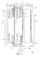
- Fig. 1 is a schematic top view of a touch panel according to an embodiment of the invention.
- Fig. 1 is a schematic top view of a touch panel according to an embodiment of the invention.
- a touch panel 100 of the present embodiment includes a substrate 110, a plurality of conductive lines Ry 1 to Ry i , a plurality of conductive pads Tx 1 to Tx N , a plurality of connecting lines CL 1 to CL N , a plurality of ground lines GL 1 to GL N and a plurality of dummy pads 160.
- the conductive lines Ry 1 to Ry i are arranged abreast on a first surface 112 of the substrate 110 and respectively extended along a first direction D1.
- the conductive pads Tx 1 to Tx N are also disposed on the first surface 112.
- the plurality of conductive pads Tx 1 are arranged along a second direction D2 and a first sensing string is formed by cascading the plurality of connecting lines CL 1 .
- the conductive pads Tx 2 ,..., Tx N adopt the same layout for respectively forming 2-N sensing series along the second direction D2.
- the first direction D1 is vertical to the second direction D2.
- amounts of the conductive lines Ry 1 to Ry i may equal to or not equal to amounts of the conductive pads Tx 1 to Tx N
- the amounts of the conductive lines Ry 1 to Ry i and the amounts of the conductive pads Tx 1 to Tx N are not particularly limited in the application.
- the conductive lines Ry 1 to Ry i and the conductive pads Tx 1 to Tx N are alternately disposed in order to accomplish a sensing process in terms of planes.
- the conductive lines Ry 1 to Ry i and the conductive pads Tx 1 to Tx N may cause variation in capacitance on a contact position where the finger touches.
- the touch panel 100 may calculate a coordinate of the contact position using said variation in capacitance and transmit the coordinate to an electronic device connected thereto.
- the touch panel 100 may generate a visual difference.
- a thickness of the touch panel 100 may be reduced and a transmittance thereof may be increased, accordingly.
- the touch panel 100 when the touch panel 100 is integrated with a display panel as a display having a touch-control function, the touch panel 100 may have better optical properties.
- Fig. 1 Two adjacent conductive lines Ry 1 and Ry 2 and devices therebetween as illustrated in Fig. 1 are provided hereinafter to further describe a structure arrangement in the touch panel 100.
- structure arrangement is not only adapted for being disposed between the conductive lines Ry 1 and Ry 2 , but also adapted for applying extendedly to the touch panel 100 entirely.
- N conductive pads Tx 1 to Tx N are presented between the two adjacent conductive lines Ry 1 and Ry 2 .
- the connecting lines CL 1 to CL N are disposed on the first surface 112 and respectively connected to the conductive pads Tx 1 to Tx N .
- the conductive pads Tx 1 to Tx N located between the conductive lines Ry 1 and Ry 2 are respectively connected to the connecting lines CL 1 to CL N .
- the connecting lines CL 1 to CL N are arranged abreast and located between the conductive pads Tx 1 to Tx N and the conductive line Ry 2 , and all connecting lines CL 1 on the substrate 110 are electrically connected to each other to form the first sensing series by connecting with all pads Tx 1 on the second direction D2.
- the connecting lines CL 2 ,..., CL N may adopt the same layout for respectively forming the 2 to N sensing series.
- the connecting lines CL 1 to CL N are configured for transmitting a sensing signal generated by the conductive lines Ry 1 to Ry i and the conductive pads Tx 1 to Tx N to a control circuit and transmit a control signal outputted from the control circuit to the conductive lines Ry 1 to Ry i and the conductive pads Tx 1 to Tx N .
- the connecting lines CL 1 to CL N may extend to a bridge area 114 of the touch panel 100, and the connecting lines CL 1 to CL N are electrically connected along the second direction D2 through bridging devices on the bridge area 114 for respectively forming said 1 to N sensing series.
- the touch panel 100 includes a first bridge area 114 and a second bridge area 116 respectively located one two opposite sides of the substrate 110.
- the touch panel 100 further includes a first flexible printed circuit board 170a and a second flexible printed circuit board 170b respectively disposed on the first bridge area 114 and the second bridge area 116, and the first flexible printed circuit board 170a and the second flexible printed circuit board 170b are electrically connected to each other.
- a portion of the connecting lines CL 1 to CL N are electrically connected to the first flexible printed circuit board 170a, whereas another portion for the connecting lines CL 1 to CL N are electrically connected to the second flexible printed circuit board 170b.
- the connecting lines CL 1 to CL N may also be connected to a same side of the substrate 110.
- Such configuration may be accomplished, for example, by disposing a flexible printed circuit board on a bridge area of the touch panel, in which the bridge area is located on a side of the substrate 110, and the connecting lines CL 1 to CL N are electrically connected to the flexible printed circuit board.
- a material of the connecting lines CL 1 to CL N may be conductive transparent materials such as Indium Tin Oxide (ITO), Indium Zinc Oxide (IZO), Al doped zinc oxide (AZO) or Indium Oxide or a combination thereof.
- ITO Indium Tin Oxide
- IZO Indium Zinc Oxide
- AZO Al doped zinc oxide
- the conductive lines Ry 1 to Ry i have an identical width and the conductive pads Tx i to Tx N also have an identical size.
- the application is not limited thereto.
- the conductive pads Tx 1 to Tx N may also have a different size, which may be adjusted based on requirements such as contact area (such as size of the finger) or sensing resolution.
- the ground lines GL 1 to GL i-1 are arranged abreast on the first surface 112 and extended along the first direction D1.
- the ground lines GL 1 to GL i-1 are respectively disposed between the conductive lines and connecting lines adjacent thereto, so as to reduce poor sensing sensitivity due to electrical interference generated by the conductive lines and adjacent connecting lines.
- the ground line GL 1 is located between the conductive line Ry 2 and the corresponding connecting lines CL 1 to CL N , so as to avoid interference of the conductive line Ry 2 the corresponding connecting lines CL 1 to CL N .
- the touch panel 100 may face problems such as difficulty in fabricating process and an uneven transmittance.
- dummy pads 160 are disposed between the conductive lines and the corresponding 1 to N conductive pads to adjust the distance between the conductive lines Ry 1 to Ry i and the corresponding conductive pads Tx 1 to Tx N , so that touch panel 100 may operate normally, and degree of uniformity in transmittance of the touch panel 100 may also be maintained.
- the dummy pads 160 are only used to space apart the conductive lines Ry 1 to Ry i and the corresponding conductive pads Tx 1 to Tx N without participating the circuitry layout.
- the application in order to adjust a distance between the conductive lines and the corresponding conductive pads, the application is directed to dispose a plurality of dummy pads without participating circuitry layout to be located between the conductive lines and the corresponding conductive pads on the touch panel, so as to reduce parasitic capacitance generated between the conductive lines and the corresponding conductive pads. Further, by disposing the dummy pads between the conductive lines and the corresponding conductive pads, the uneven transmittance (caused by the distance between the conductive lines and the corresponding conductive pads being too long) while disposing the touch panel on the backlight module may also further be reduced. Moreover, the application is further directed to dispose ground lines between the conductive lines and the corresponding connecting lines, so as to reduce poor signal transmission due to interference between two adjacent conductive lines which are arranged abreast.
Landscapes
- Engineering & Computer Science (AREA)
- General Engineering & Computer Science (AREA)
- Theoretical Computer Science (AREA)
- Human Computer Interaction (AREA)
- Physics & Mathematics (AREA)
- General Physics & Mathematics (AREA)
- Position Input By Displaying (AREA)
Abstract
Description
- This application claims the priority benefits of
U.S. provisional application serial no. 61/583,205, filed on January 5, 2012 - The application relates to a touch panel, and more particularly, to a capacitive touch panel.
- As information technology, wireless mobile communication and information appliances have been rapidly developed and applied, to achieve more convenience, more small volume, light weight and more user-friendly designs, various information products have changed from using conventional input devices such as key boards or mice to using touch panels.
- Based on different sensing types, a touch sensing panel can be generally categorized into a resistive touch sensing panel, a capacitive touch sensing panel, an optical touch sensing panel, an acoustic-wave touch sensing panel, and an electromagnetic touch sensing panel. In comparison to other touch panels, the capacitive touch sensing panel is characterized by short response speed, favorable reliability, high definition, and so on. Therefore, the capacitive touch panel is widely used in the electronic products.
- The present application is directed to a touch panel capable of enhancing quality of signal transmission and sensing sensitivity.
- The application provides a touch panel, including a substrate, a plurality of conductive lines, a plurality of conductive pads, a plurality of connecting lines, a plurality of ground lines and a plurality of dummy pads. The substrate has a first surface. The conductive lines are arranged abreast on the first surface and respectively extended along a first direction. The conductive pads are disposed on the first surface, in which N conductive pads are present between two adjacent conductive lines. The connecting lines are disposed on the first surface and respectively connected to the conductive pads. In which, 1 to N conductive pads located between an i-th conductive line to a (i+1)-th conductive line are respectively connected to 1 to N connecting lines. The 1 to N connecting lines are arranged abreast and located between the 1 to N conductive pads and the (i+1)-th conductive line. j and n are positive integers. The ground lines are arranged abreast on the first surface and respectively extended along a first direction, in which an i-th ground line is located between the (i+1)-th conductive line and the corresponding 1 to N connecting lines. The dummy pads are disposed on the first surface and located between the (i+1)-th conductive line and the corresponding 1 to N connecting pads.
- In view of above, in order to adjust a distance between the conductive lines and the corresponding conductive pads, the application is directed to dispose a plurality of dummy pads without participating circuitry layout to be located between the conductive lines and the corresponding conductive pads on the touch panel, so as to reduce parasitic capacitance generated between the conductive lines and the corresponding conductive pads. Further, by disposing the dummy pads between the conductive lines and the corresponding conductive pads, the uneven transmittance (caused by the distance between the conductive lines and the corresponding conductive pads being too long) while disposing the touch panel on the backlight module may also further be reduced. Moreover, the application is further directed to dispose ground lines between the conductive lines and the corresponding connecting lines, so as to reduce poor signal transmission due to interference between two adjacent conductive lines which are arranged abreast.
- To make the above features and advantages of the invention more comprehensible, several embodiments accompanied with drawings are described in detail as follows.
-
Fig. 1 is a schematic top view of a touch panel according to an embodiment of the invention. -
Fig. 1 is a schematic top view of a touch panel according to an embodiment of the invention. Referring toFig. 1 , atouch panel 100 of the present embodiment includes asubstrate 110, a plurality of conductive lines Ry1 to Ryi, a plurality of conductive pads Tx1 to TxN, a plurality of connecting lines CL1 to CLN, a plurality of ground lines GL1 to GLN and a plurality ofdummy pads 160. The conductive lines Ry1 to Ryi are arranged abreast on afirst surface 112 of thesubstrate 110 and respectively extended along a first direction D1. The conductive pads Tx1 to TxN are also disposed on thefirst surface 112. More specifically, the plurality of conductive pads Tx1 are arranged along a second direction D2 and a first sensing string is formed by cascading the plurality of connecting lines CL1. Similarly, the conductive pads Tx2,..., TxN adopt the same layout for respectively forming 2-N sensing series along the second direction D2. In which the first direction D1 is vertical to the second direction D2. Herein, in thetouch panel 100, amounts of the conductive lines Ry1 to Ryi may equal to or not equal to amounts of the conductive pads Tx1 to TxN, the amounts of the conductive lines Ry1 to Ryi and the amounts of the conductive pads Tx1 to TxN are not particularly limited in the application. - Accordingly, the conductive lines Ry1 to Ryi and the conductive pads Tx1 to TxN are alternately disposed in order to accomplish a sensing process in terms of planes. When a user touches the
touch panel 100 with a finger, the conductive lines Ry1 to Ryi and the conductive pads Tx1 to TxN may cause variation in capacitance on a contact position where the finger touches. Thetouch panel 100 may calculate a coordinate of the contact position using said variation in capacitance and transmit the coordinate to an electronic device connected thereto. Generally, if the conductive lines Ry1 to Ryi and the conductive pads Tx1 to TxN are alternately disposed on different planes, thetouch panel 100 may generate a visual difference. Therefore, in the present embodiment, by disposing the conductive lines Ry1 to Ryi and the conductive pads Tx1 to TxN on the same plane, a thickness of thetouch panel 100 may be reduced and a transmittance thereof may be increased, accordingly. As a result, when thetouch panel 100 is integrated with a display panel as a display having a touch-control function, thetouch panel 100 may have better optical properties. - Two adjacent conductive lines Ry1 and Ry2 and devices therebetween as illustrated in
Fig. 1 are provided hereinafter to further describe a structure arrangement in thetouch panel 100. However, such structure arrangement is not only adapted for being disposed between the conductive lines Ry1 and Ry2, but also adapted for applying extendedly to thetouch panel 100 entirely. - As shown in
Fig. 1 , N conductive pads Tx1 to TxN are presented between the two adjacent conductive lines Ry1 and Ry2. The connecting lines CL1 to CLN are disposed on thefirst surface 112 and respectively connected to the conductive pads Tx1 to TxN. In other words, the conductive pads Tx1 to TxN located between the conductive lines Ry1 and Ry2 are respectively connected to the connecting lines CL1 to CLN. The connecting lines CL1 to CLN are arranged abreast and located between the conductive pads Tx1 to TxN and the conductive line Ry2, and all connecting lines CL1 on thesubstrate 110 are electrically connected to each other to form the first sensing series by connecting with all pads Tx1 on the second direction D2. Similarly, the connecting lines CL2,..., CLN may adopt the same layout for respectively forming the 2 to N sensing series. The connecting lines CL1 to CLN are configured for transmitting a sensing signal generated by the conductive lines Ry1 to Ryi and the conductive pads Tx1 to TxN to a control circuit and transmit a control signal outputted from the control circuit to the conductive lines Ry1 to Ryi and the conductive pads Tx1 to TxN. - Accordingly, the connecting lines CL1 to CLN may extend to a
bridge area 114 of thetouch panel 100, and the connecting lines CL1 to CLN are electrically connected along the second direction D2 through bridging devices on thebridge area 114 for respectively forming said 1 to N sensing series. In the present embodiment, thetouch panel 100 includes afirst bridge area 114 and asecond bridge area 116 respectively located one two opposite sides of thesubstrate 110. Thetouch panel 100 further includes a first flexible printed circuit board 170a and a second flexible printedcircuit board 170b respectively disposed on thefirst bridge area 114 and thesecond bridge area 116, and the first flexible printed circuit board 170a and the second flexible printedcircuit board 170b are electrically connected to each other. A portion of the connecting lines CL1 to CLN are electrically connected to the first flexible printed circuit board 170a, whereas another portion for the connecting lines CL1 to CLN are electrically connected to the second flexible printedcircuit board 170b. According to such configuration, since all connecting lines CL1 to CLN are respectively connected to thebridge areas substrate 110, wiring space on thetouch panel 100 may be greatly reduced, thereby reducing overall size of thetouch panel 100. Nonetheless, the application is not limited thereto. According to other embodiments of the invention, the connecting lines CL1 to CLN may also be connected to a same side of thesubstrate 110. Such configuration may be accomplished, for example, by disposing a flexible printed circuit board on a bridge area of the touch panel, in which the bridge area is located on a side of thesubstrate 110, and the connecting lines CL1 to CLN are electrically connected to the flexible printed circuit board. - In the present embodiment, a material of the connecting lines CL1 to CLN may be conductive transparent materials such as Indium Tin Oxide (ITO), Indium Zinc Oxide (IZO), Al doped zinc oxide (AZO) or Indium Oxide or a combination thereof. Practically, according to the present embodiment, the conductive lines Ry1 to Ryi have an identical width and the conductive pads Txi to TxN also have an identical size. However, the application is not limited thereto. According to other embodiments of the invention, the conductive pads Tx1 to TxN may also have a different size, which may be adjusted based on requirements such as contact area (such as size of the finger) or sensing resolution.
- Accordingly, in the present embodiment, the ground lines GL1 to GLi-1 are arranged abreast on the
first surface 112 and extended along the first direction D1. Particularly in the present embodiment, the ground lines GL1 to GLi-1 are respectively disposed between the conductive lines and connecting lines adjacent thereto, so as to reduce poor sensing sensitivity due to electrical interference generated by the conductive lines and adjacent connecting lines. As shown inFig. 1 , the ground line GL1 is located between the conductive line Ry2 and the corresponding connecting lines CL1 to CLN, so as to avoid interference of the conductive line Ry2 the corresponding connecting lines CL1 to CLN. - Moreover, when the conductive lines Ry1 to Ryi and the corresponding conductive pads Tx1 to TxN are too close to each other, parasitic capacitance generated therebetween may affect normal operation of the touch panel. Therefore, a proper distance is required to space apart the conductive lines Ry1 to Ryi and the corresponding conductive pads Tx1 to TxN. However, in the case where the distance between the conductive lines Ry1 to Ryi and the corresponding conductive pads Tx1 to TxN is increased, the
touch panel 100 may face problems such as difficulty in fabricating process and an uneven transmittance. Accordingly, in the present embodiment,dummy pads 160 are disposed between the conductive lines and the corresponding 1 to N conductive pads to adjust the distance between the conductive lines Ry1 to Ryi and the corresponding conductive pads Tx1 to TxN, so thattouch panel 100 may operate normally, and degree of uniformity in transmittance of thetouch panel 100 may also be maintained. Herein, thedummy pads 160 are only used to space apart the conductive lines Ry1 to Ryi and the corresponding conductive pads Tx1 to TxN without participating the circuitry layout. - In view of above, in order to adjust a distance between the conductive lines and the corresponding conductive pads, the application is directed to dispose a plurality of dummy pads without participating circuitry layout to be located between the conductive lines and the corresponding conductive pads on the touch panel, so as to reduce parasitic capacitance generated between the conductive lines and the corresponding conductive pads. Further, by disposing the dummy pads between the conductive lines and the corresponding conductive pads, the uneven transmittance (caused by the distance between the conductive lines and the corresponding conductive pads being too long) while disposing the touch panel on the backlight module may also further be reduced. Moreover, the application is further directed to dispose ground lines between the conductive lines and the corresponding connecting lines, so as to reduce poor signal transmission due to interference between two adjacent conductive lines which are arranged abreast.
- Although the invention has been described with reference to the above embodiments, it is apparent to one of the ordinary skill in the art that modifications to the described embodiments may be made without departing from the spirit of the invention. Accordingly, the scope of the invention will be defined by the attached claims not by the above detailed descriptions.
Claims (9)
- A touch panel, comprising:a substrate having a first surface;a plurality of conductive lines arranged abreast on the first surface and respectively extended along a first direction;a plurality of conductive pads disposed on the first surface, wherein N conductive pads are present between two adjacent conductive lines;a plurality of connecting lines disposed on the first surface and respectively connected to the conductive pads, wherein 1 to N conductive pads located between an i-th conductive line and a (i+1)-th conductive line are respectively connected to 1 to N connecting lines, the 1 to N connecting lines are arranged abreast and located between the 1 to N conductive pads and the (i+1)-th conductive line, and all of j-th connecting lines on the substrate are electrically connected to each other, wherein j and i are positive integers;a plurality of ground lines arranged abreast on the first surface and respectively extended along a first direction, wherein an i-th ground line is located between the (i+1)-th conductive line and the corresponding 1 to N connecting lines; anda plurality of dummy pads disposed on the first surface and located between the (i+1)-th conductive line and the corresponding 1 to N connecting pads;
- The touch panel of claim 1, wherein the 1 to N connecting lines are extended to the same side of the substrate.
- The touch panel of claim 2, further comprising a flexible printed circuit board disposed on the same side of the substrate, and the 1 to N connecting line are respectively electrically connected to the flexible printed circuit board.
- The touch panel of claim 1, wherein a portion of the 1 to N connecting lines is extended to a first side of the substrate and another portion of the 1 to N connecting lines is extended to a second side opposite to the first side of the substrate.
- The touch panel of claim 4, further comprising a first flexible printed circuit board and a second flexible printed circuit board, the first flexible printed circuit board and the second flexible printed circuit board are electrically connected to each other and respectively disposed on the first side of the substrate and the second side of the substrate opposite to the first side, a portion of the 1 to N connecting lines is electrically connected to the first flexible printed circuit boards, and a remaining portion of the 1 to N connecting lines is electrically connected to the second flexible printed circuit board.
- The touch panel of claim 1, wherein a material of the connecting lines comprises conductive transparent materials.
- The touch panel of claim 1, wherein the conductive lines have an identical width.
- The touch panel of claim 1, wherein the conductive pads have an identical size.
- The touch panel of claim 1, wherein the conductive pads have different sizes.
Applications Claiming Priority (2)
| Application Number | Priority Date | Filing Date | Title |
|---|---|---|---|
| US201261583205P | 2012-01-05 | 2012-01-05 | |
| US13/629,614 US20130176239A1 (en) | 2012-01-05 | 2012-09-28 | Touch panel |
Publications (1)
| Publication Number | Publication Date |
|---|---|
| EP2618243A1 true EP2618243A1 (en) | 2013-07-24 |
Family
ID=47594463
Family Applications (1)
| Application Number | Title | Priority Date | Filing Date |
|---|---|---|---|
| EP13000032.6A Withdrawn EP2618243A1 (en) | 2012-01-05 | 2013-01-04 | Touch panel |
Country Status (2)
| Country | Link |
|---|---|
| US (1) | US20130176239A1 (en) |
| EP (1) | EP2618243A1 (en) |
Families Citing this family (3)
| Publication number | Priority date | Publication date | Assignee | Title |
|---|---|---|---|---|
| KR101453026B1 (en) * | 2012-06-04 | 2014-11-03 | 주식회사 아이피시티 | Touch detecting apparatus for reducing parasitic capacitance |
| KR102792468B1 (en) * | 2019-07-24 | 2025-04-08 | 엘지디스플레이 주식회사 | Display apparatus having touch electrodes |
| KR102741706B1 (en) | 2019-12-30 | 2024-12-12 | 엘지디스플레이 주식회사 | Touch display device |
Citations (4)
| Publication number | Priority date | Publication date | Assignee | Title |
|---|---|---|---|---|
| US20100044122A1 (en) * | 2008-04-10 | 2010-02-25 | Atmel Corporation | Capacitive Touch Screen with Noise Suppression |
| US20100258360A1 (en) * | 2009-04-14 | 2010-10-14 | Atmel Corporation | Two-Dimensional Position Sensor |
| US20100309160A1 (en) * | 2009-06-09 | 2010-12-09 | Teh-Zheng Lin | Capacitive sensing assembly of touch panel |
| US20110316567A1 (en) * | 2010-01-15 | 2011-12-29 | Cypress Semiconductor Corporation | Lattice Structure for Capacitance Sensing Electrodes |
Family Cites Families (3)
| Publication number | Priority date | Publication date | Assignee | Title |
|---|---|---|---|---|
| US20020034930A1 (en) * | 2000-09-11 | 2002-03-21 | Shunpei Yamazaki | Electronic device and method of usage thereof |
| JP4357868B2 (en) * | 2003-04-25 | 2009-11-04 | シャープ株式会社 | Display device |
| WO2010084642A1 (en) * | 2009-01-26 | 2010-07-29 | シャープ株式会社 | Touch panel incorporated into display device |
-
2012
- 2012-09-28 US US13/629,614 patent/US20130176239A1/en not_active Abandoned
-
2013
- 2013-01-04 EP EP13000032.6A patent/EP2618243A1/en not_active Withdrawn
Patent Citations (4)
| Publication number | Priority date | Publication date | Assignee | Title |
|---|---|---|---|---|
| US20100044122A1 (en) * | 2008-04-10 | 2010-02-25 | Atmel Corporation | Capacitive Touch Screen with Noise Suppression |
| US20100258360A1 (en) * | 2009-04-14 | 2010-10-14 | Atmel Corporation | Two-Dimensional Position Sensor |
| US20100309160A1 (en) * | 2009-06-09 | 2010-12-09 | Teh-Zheng Lin | Capacitive sensing assembly of touch panel |
| US20110316567A1 (en) * | 2010-01-15 | 2011-12-29 | Cypress Semiconductor Corporation | Lattice Structure for Capacitance Sensing Electrodes |
Also Published As
| Publication number | Publication date |
|---|---|
| US20130176239A1 (en) | 2013-07-11 |
Similar Documents
| Publication | Publication Date | Title |
|---|---|---|
| CN205071053U (en) | smart phone | |
| US8614680B2 (en) | Touch substrate and touch display panel | |
| EP2613235B1 (en) | Touch panel and a manufacturing method thereof | |
| CN102135833B (en) | touch panel | |
| EP2818992B1 (en) | Touch-control display device with integration of capacitive and electromagnetic touch units | |
| US20110315536A1 (en) | Touch panel | |
| CN106249979A (en) | Touch electrode structure and touch control display apparatus | |
| US20110157043A1 (en) | Active device array substrate and touch display panel | |
| CN106325579A (en) | Pressure sensing input device | |
| KR20150106085A (en) | Touch panel | |
| CN104635976A (en) | Touch screen panel and display device | |
| CN106662942A (en) | Display unit with touch panel | |
| CN106201036B (en) | In-cell touch display screen and touch display screen module | |
| US8816232B2 (en) | Touch panel | |
| US9542018B2 (en) | Touch panel and electronic apparatus | |
| CN202649986U (en) | capacitive touch device | |
| US9362060B2 (en) | Touch electrode device | |
| US20130176239A1 (en) | Touch panel | |
| US20170131818A1 (en) | Touch and pressure sensing device | |
| US9454029B2 (en) | Touch-sensing liquid crystal panel | |
| TWI472978B (en) | Touch panel | |
| CN207676323U (en) | Touch display module with independent touch keys | |
| KR100368688B1 (en) | Structure of arrangement of signal wire the substrate in touch panel | |
| TWI453643B (en) | Touch panel and electronic device | |
| CN111813251A (en) | Touch panel and touch display device |
Legal Events
| Date | Code | Title | Description |
|---|---|---|---|
| PUAI | Public reference made under article 153(3) epc to a published international application that has entered the european phase |
Free format text: ORIGINAL CODE: 0009012 |
|
| 17P | Request for examination filed |
Effective date: 20130104 |
|
| AK | Designated contracting states |
Kind code of ref document: A1 Designated state(s): AL AT BE BG CH CY CZ DE DK EE ES FI FR GB GR HR HU IE IS IT LI LT LU LV MC MK MT NL NO PL PT RO RS SE SI SK SM TR |
|
| AX | Request for extension of the european patent |
Extension state: BA ME |
|
| 17Q | First examination report despatched |
Effective date: 20130702 |
|
| RBV | Designated contracting states (corrected) |
Designated state(s): AL AT BE BG CH CY CZ DE DK EE ES FI FR GB GR HR HU IE IS IT LI LT LU LV MC MK MT NL NO PL PT RO RS SE SI SK SM TR |
|
| RAP1 | Party data changed (applicant data changed or rights of an application transferred) |
Owner name: HTC CORPORATION |
|
| STAA | Information on the status of an ep patent application or granted ep patent |
Free format text: STATUS: THE APPLICATION IS DEEMED TO BE WITHDRAWN |
|
| 18D | Application deemed to be withdrawn |
Effective date: 20160419 |