EP2617514A1 - Laser processing method - Google Patents
Laser processing method Download PDFInfo
- Publication number
- EP2617514A1 EP2617514A1 EP11825100.8A EP11825100A EP2617514A1 EP 2617514 A1 EP2617514 A1 EP 2617514A1 EP 11825100 A EP11825100 A EP 11825100A EP 2617514 A1 EP2617514 A1 EP 2617514A1
- Authority
- EP
- European Patent Office
- Prior art keywords
- pulsed light
- laser
- pulsed
- thin film
- metal thin
- Prior art date
- Legal status (The legal status is an assumption and is not a legal conclusion. Google has not performed a legal analysis and makes no representation as to the accuracy of the status listed.)
- Withdrawn
Links
Images






Classifications
-
- H—ELECTRICITY
- H01—ELECTRIC ELEMENTS
- H01S—DEVICES USING THE PROCESS OF LIGHT AMPLIFICATION BY STIMULATED EMISSION OF RADIATION [LASER] TO AMPLIFY OR GENERATE LIGHT; DEVICES USING STIMULATED EMISSION OF ELECTROMAGNETIC RADIATION IN WAVE RANGES OTHER THAN OPTICAL
- H01S5/00—Semiconductor lasers
- H01S5/04—Processes or apparatus for excitation, e.g. pumping, e.g. by electron beams
- H01S5/042—Electrical excitation ; Circuits therefor
- H01S5/0427—Electrical excitation ; Circuits therefor for applying modulation to the laser
-
- B—PERFORMING OPERATIONS; TRANSPORTING
- B23—MACHINE TOOLS; METAL-WORKING NOT OTHERWISE PROVIDED FOR
- B23K—SOLDERING OR UNSOLDERING; WELDING; CLADDING OR PLATING BY SOLDERING OR WELDING; CUTTING BY APPLYING HEAT LOCALLY, e.g. FLAME CUTTING; WORKING BY LASER BEAM
- B23K26/00—Working by laser beam, e.g. welding, cutting or boring
- B23K26/02—Positioning or observing the workpiece, e.g. with respect to the point of impact; Aligning, aiming or focusing the laser beam
- B23K26/06—Shaping the laser beam, e.g. by masks or multi-focusing
- B23K26/073—Shaping the laser spot
- B23K26/0732—Shaping the laser spot into a rectangular shape
-
- B—PERFORMING OPERATIONS; TRANSPORTING
- B23—MACHINE TOOLS; METAL-WORKING NOT OTHERWISE PROVIDED FOR
- B23K—SOLDERING OR UNSOLDERING; WELDING; CLADDING OR PLATING BY SOLDERING OR WELDING; CUTTING BY APPLYING HEAT LOCALLY, e.g. FLAME CUTTING; WORKING BY LASER BEAM
- B23K26/00—Working by laser beam, e.g. welding, cutting or boring
- B23K26/36—Removing material
- B23K26/361—Removing material for deburring or mechanical trimming
-
- B—PERFORMING OPERATIONS; TRANSPORTING
- B23—MACHINE TOOLS; METAL-WORKING NOT OTHERWISE PROVIDED FOR
- B23K—SOLDERING OR UNSOLDERING; WELDING; CLADDING OR PLATING BY SOLDERING OR WELDING; CUTTING BY APPLYING HEAT LOCALLY, e.g. FLAME CUTTING; WORKING BY LASER BEAM
- B23K26/00—Working by laser beam, e.g. welding, cutting or boring
- B23K26/36—Removing material
- B23K26/40—Removing material taking account of the properties of the material involved
-
- B—PERFORMING OPERATIONS; TRANSPORTING
- B23—MACHINE TOOLS; METAL-WORKING NOT OTHERWISE PROVIDED FOR
- B23K—SOLDERING OR UNSOLDERING; WELDING; CLADDING OR PLATING BY SOLDERING OR WELDING; CUTTING BY APPLYING HEAT LOCALLY, e.g. FLAME CUTTING; WORKING BY LASER BEAM
- B23K26/00—Working by laser beam, e.g. welding, cutting or boring
- B23K26/50—Working by transmitting the laser beam through or within the workpiece
- B23K26/57—Working by transmitting the laser beam through or within the workpiece the laser beam entering a face of the workpiece from which it is transmitted through the workpiece material to work on a different workpiece face, e.g. for effecting removal, fusion splicing, modifying or reforming
-
- H—ELECTRICITY
- H01—ELECTRIC ELEMENTS
- H01S—DEVICES USING THE PROCESS OF LIGHT AMPLIFICATION BY STIMULATED EMISSION OF RADIATION [LASER] TO AMPLIFY OR GENERATE LIGHT; DEVICES USING STIMULATED EMISSION OF ELECTROMAGNETIC RADIATION IN WAVE RANGES OTHER THAN OPTICAL
- H01S3/00—Lasers, i.e. devices using stimulated emission of electromagnetic radiation in the infrared, visible or ultraviolet wave range
- H01S3/23—Arrangements of two or more lasers not provided for in groups H01S3/02 - H01S3/22, e.g. tandem arrangements of separate active media
- H01S3/2308—Amplifier arrangements, e.g. MOPA
-
- H—ELECTRICITY
- H10—SEMICONDUCTOR DEVICES; ELECTRIC SOLID-STATE DEVICES NOT OTHERWISE PROVIDED FOR
- H10F—INORGANIC SEMICONDUCTOR DEVICES SENSITIVE TO INFRARED RADIATION, LIGHT, ELECTROMAGNETIC RADIATION OF SHORTER WAVELENGTH OR CORPUSCULAR RADIATION
- H10F19/00—Integrated devices, or assemblies of multiple devices, comprising at least one photovoltaic cell covered by group H10F10/00, e.g. photovoltaic modules
- H10F19/30—Integrated devices, or assemblies of multiple devices, comprising at least one photovoltaic cell covered by group H10F10/00, e.g. photovoltaic modules comprising thin-film photovoltaic cells
- H10F19/31—Integrated devices, or assemblies of multiple devices, comprising at least one photovoltaic cell covered by group H10F10/00, e.g. photovoltaic modules comprising thin-film photovoltaic cells having multiple laterally adjacent thin-film photovoltaic cells deposited on the same substrate
- H10F19/33—Patterning processes to connect the photovoltaic cells, e.g. laser cutting of conductive or active layers
-
- B—PERFORMING OPERATIONS; TRANSPORTING
- B23—MACHINE TOOLS; METAL-WORKING NOT OTHERWISE PROVIDED FOR
- B23K—SOLDERING OR UNSOLDERING; WELDING; CLADDING OR PLATING BY SOLDERING OR WELDING; CUTTING BY APPLYING HEAT LOCALLY, e.g. FLAME CUTTING; WORKING BY LASER BEAM
- B23K2103/00—Materials to be soldered, welded or cut
- B23K2103/16—Composite materials
- B23K2103/166—Multilayered materials
- B23K2103/172—Multilayered materials wherein at least one of the layers is non-metallic
-
- B—PERFORMING OPERATIONS; TRANSPORTING
- B23—MACHINE TOOLS; METAL-WORKING NOT OTHERWISE PROVIDED FOR
- B23K—SOLDERING OR UNSOLDERING; WELDING; CLADDING OR PLATING BY SOLDERING OR WELDING; CUTTING BY APPLYING HEAT LOCALLY, e.g. FLAME CUTTING; WORKING BY LASER BEAM
- B23K2103/00—Materials to be soldered, welded or cut
- B23K2103/50—Inorganic materials other than metals or composite materials
-
- H—ELECTRICITY
- H01—ELECTRIC ELEMENTS
- H01S—DEVICES USING THE PROCESS OF LIGHT AMPLIFICATION BY STIMULATED EMISSION OF RADIATION [LASER] TO AMPLIFY OR GENERATE LIGHT; DEVICES USING STIMULATED EMISSION OF ELECTROMAGNETIC RADIATION IN WAVE RANGES OTHER THAN OPTICAL
- H01S2301/00—Functional characteristics
- H01S2301/20—Lasers with a special output beam profile or cross-section, e.g. non-Gaussian
-
- H—ELECTRICITY
- H01—ELECTRIC ELEMENTS
- H01S—DEVICES USING THE PROCESS OF LIGHT AMPLIFICATION BY STIMULATED EMISSION OF RADIATION [LASER] TO AMPLIFY OR GENERATE LIGHT; DEVICES USING STIMULATED EMISSION OF ELECTROMAGNETIC RADIATION IN WAVE RANGES OTHER THAN OPTICAL
- H01S3/00—Lasers, i.e. devices using stimulated emission of electromagnetic radiation in the infrared, visible or ultraviolet wave range
- H01S3/05—Construction or shape of optical resonators; Accommodation of active medium therein; Shape of active medium
- H01S3/06—Construction or shape of active medium
- H01S3/063—Waveguide lasers, i.e. whereby the dimensions of the waveguide are of the order of the light wavelength
- H01S3/067—Fibre lasers
- H01S3/06754—Fibre amplifiers
-
- H—ELECTRICITY
- H01—ELECTRIC ELEMENTS
- H01S—DEVICES USING THE PROCESS OF LIGHT AMPLIFICATION BY STIMULATED EMISSION OF RADIATION [LASER] TO AMPLIFY OR GENERATE LIGHT; DEVICES USING STIMULATED EMISSION OF ELECTROMAGNETIC RADIATION IN WAVE RANGES OTHER THAN OPTICAL
- H01S3/00—Lasers, i.e. devices using stimulated emission of electromagnetic radiation in the infrared, visible or ultraviolet wave range
- H01S3/14—Lasers, i.e. devices using stimulated emission of electromagnetic radiation in the infrared, visible or ultraviolet wave range characterised by the material used as the active medium
- H01S3/16—Solid materials
- H01S3/1601—Solid materials characterised by an active (lasing) ion
- H01S3/1603—Solid materials characterised by an active (lasing) ion rare earth
- H01S3/1618—Solid materials characterised by an active (lasing) ion rare earth ytterbium
-
- Y—GENERAL TAGGING OF NEW TECHNOLOGICAL DEVELOPMENTS; GENERAL TAGGING OF CROSS-SECTIONAL TECHNOLOGIES SPANNING OVER SEVERAL SECTIONS OF THE IPC; TECHNICAL SUBJECTS COVERED BY FORMER USPC CROSS-REFERENCE ART COLLECTIONS [XRACs] AND DIGESTS
- Y02—TECHNOLOGIES OR APPLICATIONS FOR MITIGATION OR ADAPTATION AGAINST CLIMATE CHANGE
- Y02E—REDUCTION OF GREENHOUSE GAS [GHG] EMISSIONS, RELATED TO ENERGY GENERATION, TRANSMISSION OR DISTRIBUTION
- Y02E10/00—Energy generation through renewable energy sources
- Y02E10/50—Photovoltaic [PV] energy
Definitions
- the present invention relates to a laser processing method.
- a pulsed laser beam is radiated onto a work piece to process the work piece.
- a laser processing technique described in Non-patent Document 1 radiates pulsed light with pulse width of approximately picoseconds onto a CIS (Copper-Indium-Diselenide, CuInSe 2 ) thin film, which is formed on a transparent glass plate, to process the thin film (ablation).
- a model "picoREGEN IC-1064-1500" manufactured by High Q Laser Inc. is used as a pulsed laser light source.
- This pulsed laser light source employs a mode lock structure, has a regenerative amplifier, and outputs pulsed light with pulse width of approximately picoseconds.
- Non-Patent Document 1 Heinz P. Huber, et al., "High speed structuring of CIS thin-film solar cells with picosecond laser ablation," Proc. of SPIE, Vol.7203, (2009 )
- a mode-lock pulsed laser light source which includes a regenerative amplifier and outputs pulsed light with pulse width of approximately picoseconds
- a pulsed laser light source is generally expensive.
- the freedom of setting the repetition frequency of a pulsed light output is restricted due to the structure of a laser resonator.
- the repetition frequency of a pulsed light output is increased up to only 30 kHz. The lower the repetition frequency of a pulsed light output is, the lower the lower the throughput of processing.
- the present invention has been developed to eliminate the problems described above. It is an object of the present invention to provide a method that is capable of performing high-throughput processing by using an inexpensive, non-mode-lock (nonresonant structure) pulsed laser light source.
- a laser processing method is a laser processing method of processing a metal thin film formed on a transparent substrate by a pulsed light radiation.
- the laser processing method has the steps of preparing a semiconductor laser, preparing a fiber laser comprising, at least, an optical amplifier and a MOPA structure (referred to as "MOPA fiber laser” hereinafter), controlling a full width at half maximum (“FWHM” hereinbelow) of amplified pulsed light in a desired range, and then radiating pulsed light from the MOPA fiber laser onto the metal thin film through the transparent substrate.
- the semiconductor laser to be prepared repeatedly outputs the pulsed light by being directly modulated in accordance with electric signals.
- the MOPA fiber laser to be prepared has at least the optical amplifier.
- the optical amplifier includes glass doped with rare earth element-added as an optical amplification medium and amplifies the pulsed light that is outputted from the semiconductor laser.
- the pulsed light that is outputted from the optical amplifier is controlled such that the FWHM thereof becomes 0.2 ns or longer but shorter than 1 ns.
- the pulsed light with the controlled FWHM is radiated from the MOPA fiber laser onto the metal thin film from the opposite side of the metal thin film with respect to the transparent substrate, whereby the metal thin film is removed.
- the laser processing method uses a pulsed laser light source having a simple and inexpensive MOPA structure.
- the FWHM of the amplified pulsed light that is outputted from the optical amplifier is controlled to be 0.2 ns or longer. In this case, damage to the transparent substrate can be provided.
- the FWHM of the amplified pulsed light that is outputted from the optical amplifier is controlled to be shorter than 1 ns, or preferably 0.5 ns or shorter.
- the metal thin film can be removed with high throughput by radiating the pulsed light from the transparent substrate side onto the metal thin film.
- the repetition frequency of an output of the pulsed light preferably exceeds 100 kHz. In this case, the throughput can be enhanced.
- an overlap ratio of spots irradiated with the pulsed light be 60% or less, and that a laser output have predetermined average power and peak power for removing the metal thin film. In this case, the processing quality can be improved.
- the overlap ratio may be set at 50% or lower.
- a spectrum of the amplified pulsed light that is outputted from the optical amplifier has a peak at a peak wavelength of a spectrum of the pulsed light that is outputted from the semiconductor laser, and has a peak also at a wavelength different from that peak wavelength. It is preferred that the pulsed light be radiated onto the metal thin film after a beam profile of the amplified pulsed light that is outputted from the optical amplifier is uniformized by beam profile uniformizing means.
- beam profile uniformizing means for example, an optical fiber that includes a core having a rectangular cross section is preferably used as the beam profile uniformizing means.
- a fluence of the pulsed light is preferably 4 J/cm 2 or more, on an irradiated surface of the transparent substrate.
- the laser processing method of the present invention is capable of performing high-throughput processing using an expensive pulsed laser light source.
- 1 pulsed laser light source; 2 ...transparent substrate; 3 ...metal thin film; 10 ... seed light source; 20 ... YbDF; 21 ... optical coupler; 22 ... pumping light source; 23, 24 ... optical isolator; 30 ... bandpass filter; 40 ... YbDF; 41 ... optical coupler; 42 ... pumping light source; 43, 44 ... optical isolator; 50 ... YbDF; 51 ... combiner; 52 to 55 ... pumping light source; and 60 ... end cap.
- Fig. 1 is a configuration example of a pulsed laser light source 1.
- the pulsed laser light source 1 shown in this diagram has a seed light source 10, a YbDF (Yb-Doped Fiber) 20, a bandpass filter 30, a YbDF 40, a YbDF 50 and the like, and has a MOPA (Master Oscillator Power Amplifier) structure.
- the pulsed laser light source 1 is of a non-mode lock state (nonresonant structure) and outputs pulsed light having a wavelength of approximately 1060 nm, which is suitable in laser processing.
- the seed light source 10 includes a semiconductor laser that is directly modulated in accordance with electric signals to repeatedly output pulsed light.
- the semiconductor laser is preferably of Fabry-Perot type in terms of providing high power and avoiding a nonlinear effect such as induced Brillouin scattering (SBS).
- SBS induced Brillouin scattering
- the semiconductor laser outputs pulsed light having a wavelength of approximately 1060 nm, which can provide benefits to the YbDFs 20, 40, 50, the amplifying optical fibers.
- the YbDFs 20, 40, 50 are optical amplification media, which are obtained by adding a Yb element (rare-earth element), serving as an active substance, to a core of an optical fiber mainly composed of silica glass.
- the YbDFs 20, 40, 50 each have a pumping light wavelength and an amplified light wavelength proximal to each other, and are advantageous in terms of providing power conversion efficiency and gaining benefits in the vicinity of the wavelength 1060 nm.
- These YbDPs 20, 40, 50 configure a three-stage optical fiber amplifier (constituting at least part of the MOPA fiber laser).
- Pumping light that is outputted from a pumping light source 22 and passes through an optical coupler 21 is supplied in a forward direction to the first-stage YbDF 20. Then, the YbDF 20 inputs pulsed light that is outputted from the seed light source 10 and passes through an optical isolator 23 and the optical coupler 21, amplifies the pulsed light, and outputs the pulsed light through an optical isolator 24.
- the bandpass filter 30 inputs the pulsed light that is outputted from the seed light source 10 and amplified by the first-stage YbDF 20, attenuates either a light spectrum on the short wavelength side from a peak wavelength of the pulsed light or a light spectrum on the long wavelength side of the same more than the other in a wavelength band of the input pulsed light, and then outputs the resultant light.
- a high-pass filter or a low-pass filter may be used in place of the bandpass filter, but the high-pass filter acts only on the long wavelength side of a seed light source spectrum, whereas the low-pass filter acts only on the short wavelength side of the seed light source spectrum.
- the bandpass filter however, has the functions of both the high-pass filter and the low-pass filter.
- Pumping light which is outputted from a pumping light source 42 and passes through an optical coupler 41, is supplied in the forward direction to the second-stage YbDF 40. Then, the YbDF 40 inputs pulsed light that is outputted from the bandpass filter 30 and passes through an optical isolator 43 and the optical coupler 41, amplifies the pulsed light, and outputs the pulsed light through an optical isolator 44. Pumping light, which is outputted from each of pumping light sources 52 to 55 and passes through a combiner 51, is supplied in the forward direction to the third-stage YbDF 50. Then, the YbDF 50 inputs and further amplifies the pulsed light amplified by the second-stage YbDF 40, and then outputs the pulsed light to the outside through an end cap 60.
- Pumping light having a pumping wavelength of 975 nm and a constant power of 200 mW is injected in a forward direction to the first-stage YbDF 20 by a core pumping method.
- the YbDF 20 to be used has a length of 5 m, and an unsaturated absorption coefficient of 240 dB/m at a wavelength of 975 nm.
- a core diameter of the YbDF 20 is 6 ⁇ m and NA thereof is approximately 0.12.
- Pumping light having a pumping wavelength of 975 nm and a constant power of 200 mW is injected in the forward direction to the second-stage YbDF 40 by the core pumping method.
- the YbDF 40 to be used has a length of 7 m and an unsaturated absorption coefficient of 240 dB/m at a wavelength of 975 nm.
- a core diameter of the YbDF 40 is 6 ⁇ m and NA thereof is approximately 0.12.
- Pumping light having a pumping wavelength of 975 nm and a power of 20 W (four pumping LDs of 5 W level) is injected in the forward direction to the third-stage YbDF 50 by a cladding pumping method.
- the YbDF 50 to be used has a length of 5 m and an unsaturated absorption coefficient of 1200 dB/m at a core part.
- a core diameter of the YbDF 50 is 10 ⁇ m and NA thereof is approximately 0.06.
- a cladding within the YbDF 50 has a diameter of 125 ⁇ m and NA of approximately 0.46.
- Such a pulsed laser light source 1 with a MOPA structure is inexpensive due to its simple structure, and a repetition frequency of a pulsed light output can be set arbitrarily.
- the pulsed laser light source 1 uses the bandpass filter 30 to attenuate either the light spectrum on the short wavelength side from the peak wavelength of the pulsed light or the light spectrum on the long wavelength side of the same more than the other, and then outputs the resultant light, the pulsed light being outputted from the seed light source 10 and amplified by the first-stage YbDF 20. Therefore, the pulsed light having its pulse width compressed into 1 ns or shorter, can be outputted.
- the laser processing method uses the pulsed laser light source 1 having the MOPA structure, and radiates pulsed light onto a metal thin film 3 on a transparent substrate 2 to process the metal thin film 3, as shown in Fig. 2 .
- the FWHM of each of pulsed light beams that are outputted from the pulsed laser light source 1 is controlled to be 0.5 ns or shorter.
- Such pulsed light beams are radiated onto the metal thin film 3 from the transparent substrate 2 side, thereby removing the metal thin film 3.
- the FWHM of each of the pulsed light beams that are outputted from the pulsed laser light source 1 be 0.2 ns or longer. It is preferred that the repetition frequency of a pulsed light output exceed 100 kHz.
- an overlap ratio of spots irradiated with the pulsed light is 60% or less, and a laser output has predetermined average power and peak power for removing the metal thin film.
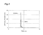
- Fig. 3 is a diagram showing an example of a waveform of the pulsed light that is outputted from the pulsed laser light source 1.
- This diagram shows a pulsed light waveform in which the repetition frequencies of a pulsed light output are 500 kHz and 2 MHz. In either case, the FWHM of the pulsed light can be reduced to 200 ps or lower.
- Fig. 4 is a SEM picture obtained when the TCO film on the transparent glass plate was removed.
- the processing conditions here are as follows: the FWHM of the pulsed light is 200 ps; the repetition frequency of the pulsed light output is 150 kHz; the average power for pulsed light radiation is 6.8 W; and the scanning speed is 2000 mm/s.
- the fluence of the pulsed light here was 3.1 J/cm 2 .
- pulsed light that has an increased pulse width and a lowered pulse peak value was used.
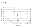
- the FWHM of the pulsed light was 0.5 ns, and the repetition frequency of the pulsed light output was 250 kHz.
- a Mo film (melting point is 2620 °C) on a transparent glass plate was removed by radiating thereon the pulsed light that has a pulse waveform shown in Fig. 5 .
- the average power for the pulsed light radiation was 5.7 W and the scanning speed was 5000 mm/s.
- the pulsed light was radiated onto the Mo film from the transparent glass plate side.
- the Mo film is formed on the transparent glass plate by means of a sputtering or CVD method, and is used in a CIS-type solar battery.
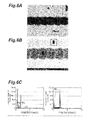
- Fig. 6 shows (a) a micrograph, (b) a SEM picture, and (c) EDX analysis results, which were obtained when the Mo film on the transparent glass plate was removed.
- the processing quality is equivalent to the processing quality obtained as a result of the process performed by radiating pulsed light having a pulse width of 10 ps as described in Non-Patent Document 1. While the scanning speed in Non-Patent Document 1 was 240 mm/s, the present embodiment achieved a scanning speed of 5000 mm/s, at least 20 times higher than that of Non-Patent Document 1.
- the fluence of the pulsed light was 4.5 J/cm 2 .
- a residue of Mo was observed when the fluence was lower than 4.5 J/cm 2 . It is considered that the reason why the above-described processing was possible with the pulse width greater than 10 ps described in Non-Patent Document 1, is because of the setting of the fluence.
- the relationship between the fluence, the pulse width and a work piece depends on a case-by-case basis, but the present embodiment illustrates the fact that the processing is possible even with an inconceivable pulse width.
- the processing conditions in this diagram are as follows: the FWHM of the pulsed light is set at 10 to 20 ns; the repetition frequency of a pulsed light output is 250 kHz; the average power for pulsed light radiation is 8 W; and the scanning speed is 5000 mm/s.
- the pulsed laser light source 1 with the configuration described above has the MOPA structure that has a semiconductor laser as the seed light source 10, the semiconductor laser having a several hundred mA drive current (over 200 mA) directly modulated. Pulsed light having a subnanosecond pulse width is outputted from the pulsed laser light source 1 in order to perform the processing. For this reason, the following advantages are obtained.
- the pulsed laser light source 1 uses the bandpass filter 30 to attenuate either the light spectrum on the short wavelength side from the peak wavelength of the pulsed light or the light spectrum on the long wavelength side of the same more than the other, and then outputs the resultant light, the pulsed light being outputted from the seed light source 10 and amplified by the first-stage YbDF 20. Therefore, the pulsed light having its pulse width compressed into subnanoseconds, can be outputted.
- a chirping component of the seed light source 10 is obtained from the pulsed laser light source 1 of Fig. 1 by the BPF, as shown by the solid line in Fig. 8 , whereby the spectrum of the pulsed light having its pulse width compressed into subnanoseconds has a sub-peak, not only at a peak wavelength of the spectrum of the pulsed light that is outputted from the semiconductor laser functioning as the seed light source 10, but also at a wavelength different than this peak wavelength, and the FWHM of the entire spectrum having the peak and the sub-peak becomes 10 nm or above.
- the value of the sub-peak is approximately half the value of the peak.
- the spectrum shown by the dashed line in the same diagram is a spectrum of pulsed light that is processed as shown in the SEM picture of Fig. 7 , and the BPF is set such that the amount of seed light source output to be transmitted becomes maximum without obtaining the chirping component shown by the solid line.
- Fig. 9 shows a spectrum waveform (light output and time) from a pulsed laser light source (having the same structure as the one shown in Fig. 1 ) different than the pulsed laser light source used in Figs. 3 and 5 .
- the FWHM of the pulse width is 0.96 ns.
- the processing quality here is equivalent to the processing quality obtained as a result of the process performed by radiating the pulsed light having a pulse width of 10 ps as described in Non-Patent Document 1.
- This processing achieved a scanning speed of 4000 mm/s.
- the repetition frequency of the pulsed light here was 150 kHz, the average power of the pulse was 8W, and the fluence was 8.9 J/cm 2 .
- Achieving a broadband spectrum shown by the solid line in Fig. 8 is beneficial in performing beam homogenization (beam profile uniformalization) by propagating pulsed light to an optical fiber that includes a core having a rectangular cross section. This is because the beam homogenization mechanism depends on realization of a multi-traverse mode. The wider the spectrum width of pulsed light is, the more it becomes possible to prevent the occurrence of speckle caused by an interference among a plurality of traverse modes, and the generation of a dark spot can be avoided.
- Fig. 11 is a diagram showing a beam profile obtained after the pulsed light having the dashed spectrum shown in Fig. 8 propagates through a rectangular core optical fiber.
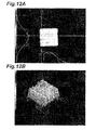
- Fig. 12 is a diagram showing a beam profile obtained after pulsed light having the solid spectrum shown in Fig. 8 propagates through the rectangular core fiber.
- the rectangular core optical fiber has a core size of 50 ⁇ m x 50 ⁇ m, NA of 0.18, and a length of 10 m.
- a V/P ratio between a minimum value (valley) and a maximum value (peak) is only 45%.
- the V/P ratio thereof was 63%. Therefore, when performing the beam homogenization using the pulsed laser light source 1 having the MOPA structure in which the directly modulated semiconductor laser functions as the seed light source, obtaining the chirping component of the seed light source 10 by means of the BPF and compressing the pulse width increases the spectrum width and therefore is beneficial in a method of laser light processing where beam homogenization is performed.
- the rolling up of the Mo film between the spots shown by the dashed circles in the SEM picture of Fig. 7 causes peeling or rolling up of the Mo film.
- One effective solution to prevent this is to perform the beam homogenization to form the cross section of pulsed light into a rectangular shape and line up rectangular spots on a Mo film.
- the examples of beam profiles shown in Figs. 11 and 12 employ simple means for directly fusing an end surface of an output fiber of a MOPA light source (a single-mode fiber with a core diameter of 10 ⁇ m to an end surface of the abovementioned rectangular core fiber.
- a space optical system may be provided therebetween when optically connecting the output fiber and the rectangular core fiber to each other, and realization of multi-traverse mode is further promoted and further improvement of the V/P ratio is expected, by focusing pulsed light emitted from the end surface of the output fiber by using a high-NA lens and joining it to the end surface of the rectangular core fiber.
- the overlap ratio may be set to be 50% or lower.
- the TCO (Transparent Conductive Oxide) film on the transparent glass plate shown in Fig. 4 was removed successfully with a pulse having a relatively wide pulse width with FWHM of approximately 5 ns when a repetition frequency of a pulsed light output was 160 kHz, the average power of pulsed light radiation was 10 W, and the scanning speed was 2500 mm/s.
- the TCO film at this time was composed of tin oxide.
- the fiber laser with a MOPA structure which directly modulates a semiconductor laser using an electric signal, outputs the resultant pulsed light repeatedly, and amplifies the light using an optical amplifier that includes rare earth element-added glass as an optical amplification medium, is favorable due to its capability of outputting a row of pulses described above and removing the TCO film on the glass or metal films such as Mo on the glass.
- the laser processing method of the present embodiment is effective not only in processing a Mo film on a transparent glass plate but also in overall processing of a relatively poorly adhesive metal film formed on a substrate made of other transparent material.
Landscapes
- Physics & Mathematics (AREA)
- Optics & Photonics (AREA)
- Engineering & Computer Science (AREA)
- Plasma & Fusion (AREA)
- Mechanical Engineering (AREA)
- Electromagnetism (AREA)
- General Physics & Mathematics (AREA)
- Condensed Matter Physics & Semiconductors (AREA)
- Chemical & Material Sciences (AREA)
- Chemical Kinetics & Catalysis (AREA)
- General Chemical & Material Sciences (AREA)
- Oil, Petroleum & Natural Gas (AREA)
- Lasers (AREA)
- Laser Beam Processing (AREA)
Abstract
Description
- The present invention relates to a laser processing method.
- A pulsed laser beam is radiated onto a work piece to process the work piece. A laser processing technique described in
Non-patent Document 1 radiates pulsed light with pulse width of approximately picoseconds onto a CIS (Copper-Indium-Diselenide, CuInSe2) thin film, which is formed on a transparent glass plate, to process the thin film (ablation). In the laser processing technique described in Non-PatentDocument 1, a model "picoREGEN IC-1064-1500" manufactured by High Q Laser Inc. is used as a pulsed laser light source. This pulsed laser light source employs a mode lock structure, has a regenerative amplifier, and outputs pulsed light with pulse width of approximately picoseconds.
Non-Patent Document 1: Heinz P. Huber, et al., "High speed structuring of CIS thin-film solar cells with picosecond laser ablation," Proc. of SPIE, Vol.7203, (2009) - The present inventors have examined the above prior art, and as a result, have discovered the following problems. Namely, a mode-lock pulsed laser light source, which includes a regenerative amplifier and outputs pulsed light with pulse width of approximately picoseconds, is generally expensive. In such a pulsed laser light source, the freedom of setting the repetition frequency of a pulsed light output is restricted due to the structure of a laser resonator. In the pulsed laser light source manufactured by High Q Laser Inc., the repetition frequency of a pulsed light output is increased up to only 30 kHz. The lower the repetition frequency of a pulsed light output is, the lower the lower the throughput of processing.
- The present invention has been developed to eliminate the problems described above. It is an object of the present invention to provide a method that is capable of performing high-throughput processing by using an inexpensive, non-mode-lock (nonresonant structure) pulsed laser light source.
- A laser processing method according to the present invention is a laser processing method of processing a metal thin film formed on a transparent substrate by a pulsed light radiation. The laser processing method has the steps of preparing a semiconductor laser, preparing a fiber laser comprising, at least, an optical amplifier and a MOPA structure (referred to as "MOPA fiber laser" hereinafter), controlling a full width at half maximum ("FWHM" hereinbelow) of amplified pulsed light in a desired range, and then radiating pulsed light from the MOPA fiber laser onto the metal thin film through the transparent substrate. The semiconductor laser to be prepared repeatedly outputs the pulsed light by being directly modulated in accordance with electric signals. The MOPA fiber laser to be prepared has at least the optical amplifier. The optical amplifier includes glass doped with rare earth element-added as an optical amplification medium and amplifies the pulsed light that is outputted from the semiconductor laser. In the MOPA fiber laser, the pulsed light that is outputted from the optical amplifier is controlled such that the FWHM thereof becomes 0.2 ns or longer but shorter than 1 ns. The pulsed light with the controlled FWHM is radiated from the MOPA fiber laser onto the metal thin film from the opposite side of the metal thin film with respect to the transparent substrate, whereby the metal thin film is removed.
- The laser processing method according to the present invention uses a pulsed laser light source having a simple and inexpensive MOPA structure. The FWHM of the amplified pulsed light that is outputted from the optical amplifier is controlled to be 0.2 ns or longer. In this case, damage to the transparent substrate can be provided. On the other hand, the FWHM of the amplified pulsed light that is outputted from the optical amplifier is controlled to be shorter than 1 ns, or preferably 0.5 ns or shorter. The metal thin film can be removed with high throughput by radiating the pulsed light from the transparent substrate side onto the metal thin film.
- In the laser processing method according to the present invention, the repetition frequency of an output of the pulsed light preferably exceeds 100 kHz. In this case, the throughput can be enhanced.
- In the laser processing method according to the present invention, when performing a pulse scan in which a pulsed light radiation position is scanned on the metal thin film, based on a preset scanning speed and a preset repetition frequency for the pulsed light radiation, it is preferred that an overlap ratio of spots irradiated with the pulsed light be 60% or less, and that a laser output have predetermined average power and peak power for removing the metal thin film. In this case, the processing quality can be improved. Note that, when using an optical fiber that includes a core having a rectangular cross section, the overlap ratio may be set at 50% or lower.
- In the laser processing method according to the present invention, a spectrum of the amplified pulsed light that is outputted from the optical amplifier has a peak at a peak wavelength of a spectrum of the pulsed light that is outputted from the semiconductor laser, and has a peak also at a wavelength different from that peak wavelength. It is preferred that the pulsed light be radiated onto the metal thin film after a beam profile of the amplified pulsed light that is outputted from the optical amplifier is uniformized by beam profile uniformizing means. Here, for example, an optical fiber that includes a core having a rectangular cross section is preferably used as the beam profile uniformizing means. In addition, a fluence of the pulsed light is preferably 4 J/cm2 or more, on an irradiated surface of the transparent substrate.
- As described above, the laser processing method of the present invention is capable of performing high-throughput processing using an expensive pulsed laser light source.
-
-
Fig. 1 is a configuration diagram of a pulsedlaser light source 1; -
Fig. 2 is a diagram for explaining a laser processing method in which the pulsedlaser light source 1 is used; -
Fig. 3 is a diagram showing an example of a waveform of pulsed light that is outputted from the pulsedlaser light source 1; -
Fig. 4 is a SEM picture captured when a TCO film on a transparent glass plate is removed; -
Fig. 5 is a diagram showing another example of a waveform of pulsed light that is outputted from the pulsedlaser light source 1; -
Fig. 6 shows (a) a micrograph, (b) a SEM picture, and (c) EDX analysis results, which were obtained when the Mo film on the transparent glass plate was removed; -
Fig. 7 is a diagram showing a SEM picture captured when the Mo film on the transparent glass plate is removed; -
Fig. 8 is a diagram showing spectra of pulsed light outputted from the pulsedlaser light source 1; -
Fig. 9 is a diagram showing a pulse waveform from another light source of the pulsedlaser light source 1; -
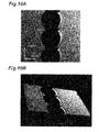
Fig. 10 shows diagrams showing (a) a SEM picture that is captured when a Mo film on a transparent glass plate is removed with a pulse having FWHM of 0.96 ns shown inFig. 9 , and (b) a three-dimensional image thereof; -
Fig. 11 shows diagrams each showing a beam profile that is obtained after pulsed light having the dashed spectrum shown inFig. 8 propagates through a rectangular core optical fiber; and -
Fig. 12 shows diagrams each showing a beam profile that is obtained after pulsed light having the solid spectrum shown inFig. 8 propagates through the rectangular core optical fiber. - 1 ... pulsed laser light source; 2 ...transparent substrate; 3 ...metal thin film; 10 ... seed light source; 20 ... YbDF; 21 ... optical coupler; 22 ... pumping light source; 23, 24 ... optical isolator; 30 ... bandpass filter; 40 ... YbDF; 41 ... optical coupler; 42 ... pumping light source; 43, 44 ... optical isolator; 50 ... YbDF; 51 ... combiner; 52 to 55 ... pumping light source; and 60 ... end cap.
- In the following, embodiments of the present invention will be described hereinafter in detail with reference to
Figs. 1 to 12 . In the description of the drawings, identical or corresponding components are designated by the same reference numerals, and overlapping description is omitted. - First of all, an example of a configuration of a pulsed laser light source that is used favorably in a laser processing method according to the present embodiment will be described.
Fig. 1 is a configuration example of a pulsedlaser light source 1. The pulsedlaser light source 1 shown in this diagram has aseed light source 10, a YbDF (Yb-Doped Fiber) 20, abandpass filter 30, aYbDF 40, aYbDF 50 and the like, and has a MOPA (Master Oscillator Power Amplifier) structure. The pulsedlaser light source 1 is of a non-mode lock state (nonresonant structure) and outputs pulsed light having a wavelength of approximately 1060 nm, which is suitable in laser processing. - The
seed light source 10 includes a semiconductor laser that is directly modulated in accordance with electric signals to repeatedly output pulsed light. The semiconductor laser is preferably of Fabry-Perot type in terms of providing high power and avoiding a nonlinear effect such as induced Brillouin scattering (SBS). Furthermore, the semiconductor laser outputs pulsed light having a wavelength of approximately 1060 nm, which can provide benefits to theYbDFs YbDFs YbDFs wavelength 1060 nm. TheseYbDPs - Pumping light that is outputted from a pumping
light source 22 and passes through anoptical coupler 21 is supplied in a forward direction to the first-stage YbDF 20. Then, theYbDF 20 inputs pulsed light that is outputted from theseed light source 10 and passes through anoptical isolator 23 and theoptical coupler 21, amplifies the pulsed light, and outputs the pulsed light through anoptical isolator 24. - The
bandpass filter 30 inputs the pulsed light that is outputted from theseed light source 10 and amplified by the first-stage YbDF 20, attenuates either a light spectrum on the short wavelength side from a peak wavelength of the pulsed light or a light spectrum on the long wavelength side of the same more than the other in a wavelength band of the input pulsed light, and then outputs the resultant light. A high-pass filter or a low-pass filter may be used in place of the bandpass filter, but the high-pass filter acts only on the long wavelength side of a seed light source spectrum, whereas the low-pass filter acts only on the short wavelength side of the seed light source spectrum. The bandpass filter, however, has the functions of both the high-pass filter and the low-pass filter. - Pumping light, which is outputted from a pumping
light source 42 and passes through anoptical coupler 41, is supplied in the forward direction to the second-stage YbDF 40. Then, theYbDF 40 inputs pulsed light that is outputted from thebandpass filter 30 and passes through anoptical isolator 43 and theoptical coupler 41, amplifies the pulsed light, and outputs the pulsed light through anoptical isolator 44. Pumping light, which is outputted from each of pumpinglight sources 52 to 55 and passes through acombiner 51, is supplied in the forward direction to the third-stage YbDF 50. Then, theYbDF 50 inputs and further amplifies the pulsed light amplified by the second-stage YbDF 40, and then outputs the pulsed light to the outside through anend cap 60. - The following describes favorable configuration examples. Pumping light having a pumping wavelength of 975 nm and a constant power of 200 mW is injected in a forward direction to the first-
stage YbDF 20 by a core pumping method. TheYbDF 20 to be used has a length of 5 m, and an unsaturated absorption coefficient of 240 dB/m at a wavelength of 975 nm. A core diameter of theYbDF 20 is 6 µm and NA thereof is approximately 0.12. Pumping light having a pumping wavelength of 975 nm and a constant power of 200 mW is injected in the forward direction to the second-stage YbDF 40 by the core pumping method. TheYbDF 40 to be used has a length of 7 m and an unsaturated absorption coefficient of 240 dB/m at a wavelength of 975 nm. A core diameter of theYbDF 40 is 6 µm and NA thereof is approximately 0.12. Pumping light having a pumping wavelength of 975 nm and a power of 20 W (four pumping LDs of 5 W level) is injected in the forward direction to the third-stage YbDF 50 by a cladding pumping method. TheYbDF 50 to be used has a length of 5 m and an unsaturated absorption coefficient of 1200 dB/m at a core part. A core diameter of theYbDF 50 is 10 µm and NA thereof is approximately 0.06. A cladding within theYbDF 50 has a diameter of 125 µm and NA of approximately 0.46. - Such a pulsed
laser light source 1 with a MOPA structure is inexpensive due to its simple structure, and a repetition frequency of a pulsed light output can be set arbitrarily. Particularly, the pulsedlaser light source 1 uses thebandpass filter 30 to attenuate either the light spectrum on the short wavelength side from the peak wavelength of the pulsed light or the light spectrum on the long wavelength side of the same more than the other, and then outputs the resultant light, the pulsed light being outputted from theseed light source 10 and amplified by the first-stage YbDF 20. Therefore, the pulsed light having its pulse width compressed into 1 ns or shorter, can be outputted. - Moreover, the laser processing method according to the present embodiment uses the pulsed
laser light source 1 having the MOPA structure, and radiates pulsed light onto a metalthin film 3 on atransparent substrate 2 to process the metalthin film 3, as shown inFig. 2 . In so doing, the FWHM of each of pulsed light beams that are outputted from the pulsedlaser light source 1 is controlled to be 0.5 ns or shorter. Such pulsed light beams are radiated onto the metalthin film 3 from thetransparent substrate 2 side, thereby removing the metalthin film 3. It is preferred that the FWHM of each of the pulsed light beams that are outputted from the pulsedlaser light source 1 be 0.2 ns or longer. It is preferred that the repetition frequency of a pulsed light output exceed 100 kHz. In addition, when performing a pulse scan in which a pulsed light radiation position is scanned on the metalthin film 3, based on a preset scanning speed and a preset repetition frequency for the pulsed light radiation, an overlap ratio of spots irradiated with the pulsed light is 60% or less, and a laser output has predetermined average power and peak power for removing the metal thin film. -
Fig. 3 is a diagram showing an example of a waveform of the pulsed light that is outputted from the pulsedlaser light source 1. This diagram shows a pulsed light waveform in which the repetition frequencies of a pulsed light output are 500 kHz and 2 MHz. In either case, the FWHM of the pulsed light can be reduced to 200 ps or lower. - However, when a TCO (Transparent Conductive Oxide) film on a transparent glass plate was removed by radiating thereon the pulsed light having the pulse waveform shown in
Fig. 3 , microscopic cracks were generated on the transparent glass plate, as shown inFig. 4. Fig. 4 is a SEM picture obtained when the TCO film on the transparent glass plate was removed. The processing conditions here are as follows: the FWHM of the pulsed light is 200 ps; the repetition frequency of the pulsed light output is 150 kHz; the average power for pulsed light radiation is 6.8 W; and the scanning speed is 2000 mm/s. The fluence of the pulsed light here was 3.1 J/cm2. - As shown in
Fig. 5 , pulsed light that has an increased pulse width and a lowered pulse peak value was used. The FWHM of the pulsed light was 0.5 ns, and the repetition frequency of the pulsed light output was 250 kHz. A Mo film (melting point is 2620 °C) on a transparent glass plate was removed by radiating thereon the pulsed light that has a pulse waveform shown inFig. 5 . The average power for the pulsed light radiation was 5.7 W and the scanning speed was 5000 mm/s. The pulsed light was radiated onto the Mo film from the transparent glass plate side. The Mo film is formed on the transparent glass plate by means of a sputtering or CVD method, and is used in a CIS-type solar battery. - Removal of the Mo film by radiating the pulsed light thereon as described above was done successfully without causing any defects such as microscopic cracks, peeling, and rolling up between spots, as shown in
Fig. 6. Fig. 6 shows (a) a micrograph, (b) a SEM picture, and (c) EDX analysis results, which were obtained when the Mo film on the transparent glass plate was removed. The processing quality is equivalent to the processing quality obtained as a result of the process performed by radiating pulsed light having a pulse width of 10 ps as described inNon-Patent Document 1. While the scanning speed inNon-Patent Document 1 was 240 mm/s, the present embodiment achieved a scanning speed of 5000 mm/s, at least 20 times higher than that ofNon-Patent Document 1. The fluence of the pulsed light was 4.5 J/cm2. A residue of Mo was observed when the fluence was lower than 4.5 J/cm2. It is considered that the reason why the above-described processing was possible with the pulse width greater than 10 ps described inNon-Patent Document 1, is because of the setting of the fluence. The relationship between the fluence, the pulse width and a work piece depends on a case-by-case basis, but the present embodiment illustrates the fact that the processing is possible even with an inconceivable pulse width. - Note that rolling up between spots is a defect where the Mo film rolls up between two adjacent pulsed light radiation spots, as shown in the dashed circles in the SEM picture shown in
Fig. 7 . The processing conditions in this diagram are as follows: the FWHM of the pulsed light is set at 10 to 20 ns; the repetition frequency of a pulsed light output is 250 kHz; the average power for pulsed light radiation is 8 W; and the scanning speed is 5000 mm/s. - Furthermore, the pulsed
laser light source 1 with the configuration described above has the MOPA structure that has a semiconductor laser as theseed light source 10, the semiconductor laser having a several hundred mA drive current (over 200 mA) directly modulated. Pulsed light having a subnanosecond pulse width is outputted from the pulsedlaser light source 1 in order to perform the processing. For this reason, the following advantages are obtained. In other words, the pulsedlaser light source 1 uses thebandpass filter 30 to attenuate either the light spectrum on the short wavelength side from the peak wavelength of the pulsed light or the light spectrum on the long wavelength side of the same more than the other, and then outputs the resultant light, the pulsed light being outputted from theseed light source 10 and amplified by the first-stage YbDF 20. Therefore, the pulsed light having its pulse width compressed into subnanoseconds, can be outputted. - As a result, a chirping component of the
seed light source 10 is obtained from the pulsedlaser light source 1 ofFig. 1 by the BPF, as shown by the solid line inFig. 8 , whereby the spectrum of the pulsed light having its pulse width compressed into subnanoseconds has a sub-peak, not only at a peak wavelength of the spectrum of the pulsed light that is outputted from the semiconductor laser functioning as theseed light source 10, but also at a wavelength different than this peak wavelength, and the FWHM of the entire spectrum having the peak and the sub-peak becomes 10 nm or above. The value of the sub-peak is approximately half the value of the peak. Note that the spectrum shown by the dashed line in the same diagram is a spectrum of pulsed light that is processed as shown in the SEM picture ofFig. 7 , and the BPF is set such that the amount of seed light source output to be transmitted becomes maximum without obtaining the chirping component shown by the solid line. -
Fig. 9 shows a spectrum waveform (light output and time) from a pulsed laser light source (having the same structure as the one shown inFig. 1 ) different than the pulsed laser light source used inFigs. 3 and5 . The FWHM of the pulse width is 0.96 ns. When the same processing as the one in the example shown inFig. 6 was performed using this pulsed light, the results shown inFig. 10 were obtained.Fig. 10 shows (a) a SEM picture captured when a Mo film on a transparent glass plate was removed, and (b) a three-dimensional image thereof. The processing quality here is equivalent to the processing quality obtained as a result of the process performed by radiating the pulsed light having a pulse width of 10 ps as described inNon-Patent Document 1. This processing achieved a scanning speed of 4000 mm/s. The repetition frequency of the pulsed light here was 150 kHz, the average power of the pulse was 8W, and the fluence was 8.9 J/cm2. - Achieving a broadband spectrum shown by the solid line in
Fig. 8 is beneficial in performing beam homogenization (beam profile uniformalization) by propagating pulsed light to an optical fiber that includes a core having a rectangular cross section. This is because the beam homogenization mechanism depends on realization of a multi-traverse mode. The wider the spectrum width of pulsed light is, the more it becomes possible to prevent the occurrence of speckle caused by an interference among a plurality of traverse modes, and the generation of a dark spot can be avoided. -
Fig. 11 is a diagram showing a beam profile obtained after the pulsed light having the dashed spectrum shown inFig. 8 propagates through a rectangular core optical fiber.Fig. 12 is a diagram showing a beam profile obtained after pulsed light having the solid spectrum shown inFig. 8 propagates through the rectangular core fiber. In either case, the rectangular core optical fiber has a core size of 50 µm x 50 µm, NA of 0.18, and a length of 10 m. - In the beam profile shown in
Fig. 11 , a V/P ratio between a minimum value (valley) and a maximum value (peak) is only 45%. In the beam profile shown inFig. 12 , on the other hand, the V/P ratio thereof was 63%. Therefore, when performing the beam homogenization using the pulsedlaser light source 1 having the MOPA structure in which the directly modulated semiconductor laser functions as the seed light source, obtaining the chirping component of theseed light source 10 by means of the BPF and compressing the pulse width increases the spectrum width and therefore is beneficial in a method of laser light processing where beam homogenization is performed. - The rolling up of the Mo film between the spots shown by the dashed circles in the SEM picture of
Fig. 7 causes peeling or rolling up of the Mo film. One effective solution to prevent this is to perform the beam homogenization to form the cross section of pulsed light into a rectangular shape and line up rectangular spots on a Mo film. - The examples of beam profiles shown in
Figs. 11 and12 employ simple means for directly fusing an end surface of an output fiber of a MOPA light source (a single-mode fiber with a core diameter of 10 µm to an end surface of the abovementioned rectangular core fiber. However, a space optical system may be provided therebetween when optically connecting the output fiber and the rectangular core fiber to each other, and realization of multi-traverse mode is further promoted and further improvement of the V/P ratio is expected, by focusing pulsed light emitted from the end surface of the output fiber by using a high-NA lens and joining it to the end surface of the rectangular core fiber. When using the rectangular core fiber, the overlap ratio may be set to be 50% or lower. - Note that the TCO (Transparent Conductive Oxide) film on the transparent glass plate shown in
Fig. 4 was removed successfully with a pulse having a relatively wide pulse width with FWHM of approximately 5 ns when a repetition frequency of a pulsed light output was 160 kHz, the average power of pulsed light radiation was 10 W, and the scanning speed was 2500 mm/s. The TCO film at this time was composed of tin oxide. In other words, the fiber laser with a MOPA structure, which directly modulates a semiconductor laser using an electric signal, outputs the resultant pulsed light repeatedly, and amplifies the light using an optical amplifier that includes rare earth element-added glass as an optical amplification medium, is favorable due to its capability of outputting a row of pulses described above and removing the TCO film on the glass or metal films such as Mo on the glass. - Note that the laser processing method of the present embodiment is effective not only in processing a Mo film on a transparent glass plate but also in overall processing of a relatively poorly adhesive metal film formed on a substrate made of other transparent material.
Claims (7)
- A laser processing method of processing a metal thin film formed on a transparent substrate by a pulsed light radiation, comprising the steps of:preparing a semiconductor laser that repeatedly outputs pulsed light by being directly modulated in accordance with electric signals;preparing a MOPA fiber laser comprising, at least, an optical amplifier that includes a glass doped with a rare earth element and amplifies the pulsed light outputted from the semiconductor laser;controlling a full width at half maximum of the pulsed light outputted from the optical amplifier to be 0.2 ns or longer but shorter than 1 ns; andremoving the metal thin film by radiating the pulsed light, emitted from the MOPA fiber laser, onto the metal thin film from the opposite side of the metal thin film with respect to the transparent substrate.
- The laser processing method according to claim 1, wherein the full width at half maximum of the pulsed light amplified by the optical amplifier is 0.5 ns or shorter.
- The laser processing method according to claim 1, wherein a repetition frequency of an output of the pulsed light exceeds 100 kHz.
- The laser processing method according to claim 1, wherein, when performing a pulsed light scan in which a pulsed light radiation position is scanned on the metal thin film, based on a preset scanning speed and a preset repetition frequency for the pulsed light radiation, an overlap ratio of spots irradiated with the pulsed light is 60%, or less and a laser output has predetermined average power and peak power for removing the metal thin film.
- The laser processing method according to claim 1, wherein a spectrum of the pulsed light amplified by the optical amplifier has a peak at a peak wavelength of a spectrum of the pulsed light outputted from the semiconductor laser, and has a peak also at a wavelength different from that peak wavelength, and
wherein the pulsed light amplified by the optical amplifier is radiated onto the metal thin film after a beam profile of the pulsed light is uniformized by beam profile uniformizing means. - The laser processing method according to claim 5, wherein the beam profile uniformizing means includes an optical fiber having a core with a rectangular cross section.
- The laser processing method according to claim 1, wherein, on an irradiated surface of the transparent substrate, a fluence of the pulsed light is 4 J/cm2 or more.
Applications Claiming Priority (3)
| Application Number | Priority Date | Filing Date | Title |
|---|---|---|---|
| JP2010206871 | 2010-09-15 | ||
| US38537310P | 2010-09-22 | 2010-09-22 | |
| PCT/JP2011/070640 WO2012036097A1 (en) | 2010-09-15 | 2011-09-09 | Laser processing method |
Publications (2)
| Publication Number | Publication Date |
|---|---|
| EP2617514A1 true EP2617514A1 (en) | 2013-07-24 |
| EP2617514A4 EP2617514A4 (en) | 2018-01-03 |
Family
ID=45831560
Family Applications (1)
| Application Number | Title | Priority Date | Filing Date |
|---|---|---|---|
| EP11825100.8A Withdrawn EP2617514A4 (en) | 2010-09-15 | 2011-09-09 | Laser processing method |
Country Status (6)
| Country | Link |
|---|---|
| US (1) | US8873595B2 (en) |
| EP (1) | EP2617514A4 (en) |
| JP (1) | JP5983407B2 (en) |
| KR (1) | KR20130101057A (en) |
| CN (1) | CN103108722B (en) |
| WO (1) | WO2012036097A1 (en) |
Cited By (1)
| Publication number | Priority date | Publication date | Assignee | Title |
|---|---|---|---|---|
| DE102016210844A1 (en) * | 2016-06-17 | 2017-12-21 | 4Jet Microtech Gmbh & Co. Kg | Device and method for removing a layer |
Families Citing this family (7)
| Publication number | Priority date | Publication date | Assignee | Title |
|---|---|---|---|---|
| JPWO2015178391A1 (en) * | 2014-05-20 | 2017-04-20 | 日本合成化学工業株式会社 | Resin sheet, resin sheet with pressure-sensitive adhesive layer, and uses using them |
| JP6261471B2 (en) * | 2014-07-31 | 2018-01-17 | 株式会社キーエンス | Laser processing equipment |
| CN104733988B (en) * | 2015-03-31 | 2016-03-02 | 深圳市创鑫激光股份有限公司 | Based on the MOPA pulse optical fiber of pulsed drive super-radiance light emitting diode |
| CR20170456A (en) | 2015-04-07 | 2018-06-13 | Intercept Pharmaceuticals Inc | PHARMACEUTICAL COMPOSITIONS FOR COMBINED THERAPIES |
| US11148228B2 (en) | 2017-07-10 | 2021-10-19 | Guardian Glass, LLC | Method of making insulated glass window units |
| WO2019062739A1 (en) * | 2017-09-29 | 2019-04-04 | (Cnbm) Bengbu Design & Research Institute For Glass Industry Co., Ltd | Semitransparent thin-film solar module |
| JP7407964B2 (en) * | 2020-09-25 | 2024-01-04 | 古河電気工業株式会社 | Laser processing method and laser processing equipment |
Family Cites Families (17)
| Publication number | Priority date | Publication date | Assignee | Title |
|---|---|---|---|---|
| US4190759A (en) * | 1975-08-27 | 1980-02-26 | Hitachi, Ltd. | Processing of photomask |
| US5710786A (en) * | 1995-08-25 | 1998-01-20 | Sdl, Inc. | Optical fibre laser pump source for fibre amplifiers |
| JP3676202B2 (en) * | 2000-07-13 | 2005-07-27 | 三菱重工業株式会社 | Method for manufacturing photovoltaic device |
| JP2002273582A (en) * | 2001-03-16 | 2002-09-25 | Ricoh Microelectronics Co Ltd | Beam processing apparatus and touch panel substrate manufacturing method |
| JP4006994B2 (en) | 2001-12-18 | 2007-11-14 | 株式会社リコー | Three-dimensional structure processing method, three-dimensional product manufacturing method, and three-dimensional structure |
| JP4064340B2 (en) * | 2003-12-25 | 2008-03-19 | 昭和シェル石油株式会社 | Manufacturing method of integrated thin film solar cell |
| US20060207976A1 (en) * | 2005-01-21 | 2006-09-21 | Bovatsek James M | Laser material micromachining with green femtosecond pulses |
| JP2007158012A (en) * | 2005-12-05 | 2007-06-21 | Hamamatsu Photonics Kk | Excitation light guide member, optical fiber structure and optical device |
| JP4954836B2 (en) * | 2006-09-21 | 2012-06-20 | 株式会社半導体エネルギー研究所 | Method for manufacturing semiconductor device |
| JP2009119521A (en) * | 2007-11-19 | 2009-06-04 | Miyachi Technos Corp | Laser welding method |
| US8290003B2 (en) * | 2007-11-30 | 2012-10-16 | Sumitomo Electric Industries, Ltd. | Pulse light source |
| JP2009168914A (en) * | 2008-01-11 | 2009-07-30 | Mitsubishi Cable Ind Ltd | Optical fiber and method for manufacturing the same |
| JP2009172629A (en) * | 2008-01-23 | 2009-08-06 | Miyachi Technos Corp | Marking apparatus and marking method |
| JP2010087041A (en) * | 2008-09-29 | 2010-04-15 | Ulvac Japan Ltd | Method of removing thin film by laser beam, and method of manufacturing thin-film solar cell panel |
| JP5454080B2 (en) * | 2008-10-23 | 2014-03-26 | 住友電気工業株式会社 | Laser processing method and laser processing apparatus |
| JP2010125489A (en) * | 2008-11-28 | 2010-06-10 | Keyence Corp | Laser marker and laser marking system |
| JP5338334B2 (en) * | 2009-01-21 | 2013-11-13 | オムロン株式会社 | Laser light source device and laser processing device |
-
2011
- 2011-09-09 CN CN201180044627.1A patent/CN103108722B/en not_active Expired - Fee Related
- 2011-09-09 WO PCT/JP2011/070640 patent/WO2012036097A1/en not_active Ceased
- 2011-09-09 EP EP11825100.8A patent/EP2617514A4/en not_active Withdrawn
- 2011-09-09 KR KR1020137009492A patent/KR20130101057A/en not_active Ceased
- 2011-09-09 JP JP2012533982A patent/JP5983407B2/en not_active Expired - Fee Related
- 2011-09-13 US US13/231,698 patent/US8873595B2/en not_active Expired - Fee Related
Non-Patent Citations (1)
| Title |
|---|
| See references of WO2012036097A1 * |
Cited By (1)
| Publication number | Priority date | Publication date | Assignee | Title |
|---|---|---|---|---|
| DE102016210844A1 (en) * | 2016-06-17 | 2017-12-21 | 4Jet Microtech Gmbh & Co. Kg | Device and method for removing a layer |
Also Published As
| Publication number | Publication date |
|---|---|
| US8873595B2 (en) | 2014-10-28 |
| JP5983407B2 (en) | 2016-08-31 |
| JPWO2012036097A1 (en) | 2014-02-03 |
| WO2012036097A1 (en) | 2012-03-22 |
| US20120106581A1 (en) | 2012-05-03 |
| KR20130101057A (en) | 2013-09-12 |
| EP2617514A4 (en) | 2018-01-03 |
| CN103108722A (en) | 2013-05-15 |
| CN103108722B (en) | 2015-12-02 |
Similar Documents
| Publication | Publication Date | Title |
|---|---|---|
| US8873595B2 (en) | Laser processing method | |
| US8933367B2 (en) | Laser processing method | |
| US7724787B2 (en) | Method and system for tunable pulsed laser source | |
| US9044829B2 (en) | Fiber laser systems for cold ablation | |
| KR101601344B1 (en) | Laser processing method and laser processing device | |
| CN100470347C (en) | A Narrow Pulse Fiber Amplifier | |
| US20110233177A1 (en) | Method and apparatus to scribe a line in a thin film material using a burst of laser pulses with beneficial pulse shape | |
| CN102368588B (en) | Method for improving contrast of ultrashort pulse | |
| US20080261382A1 (en) | Wafer dicing using a fiber mopa | |
| US8369004B2 (en) | MOPA light source | |
| CN110048294B (en) | Method for generating high-power intermediate infrared ultrafast pulse laser | |
| US9270075B2 (en) | Pulsed supercontinuum source of variable pulse duration | |
| US20100195193A1 (en) | Optical pulse source device | |
| CN118645870B (en) | A high-power fiber seed and solid-state amplified laser preamplifier | |
| TWI869957B (en) | Solid-state laser device and solid-state laser processing device | |
| CN102480102A (en) | MOPA (master oscillator power amplifier) light source | |
| TWM662304U (en) | Femtosecond laser source structure | |
| Yilmaz et al. | Large-mode-area Er-doped fiber chirped-pulse amplification system for high-energy sub-picosecond pulses at 1.55 µm | |
| JPWO2017222022A1 (en) | Fiber laser circuit | |
| US20230075209A1 (en) | Laser processing device and laser processing method | |
| Hu et al. | Supercontinuum Generation in the Low-Peak-Power Regime Using a Single-Stage Multipass Cell | |
| Astrauskas et al. | Laser De-Bonding from Silicon Wafers with Picosecond 2.09-μm Holmium Laser | |
| Łaszczych et al. | Fiber-Based CPA System at 2050 nm With Multi-μJ Pulse Energy at High Repetition Rate | |
| JP2004087541A (en) | High power light source unit | |
| WO2024235475A1 (en) | Metal foil cutting with pulsed fiber laser beam |
Legal Events
| Date | Code | Title | Description |
|---|---|---|---|
| PUAI | Public reference made under article 153(3) epc to a published international application that has entered the european phase |
Free format text: ORIGINAL CODE: 0009012 |
|
| 17P | Request for examination filed |
Effective date: 20130412 |
|
| AK | Designated contracting states |
Kind code of ref document: A1 Designated state(s): AL AT BE BG CH CY CZ DE DK EE ES FI FR GB GR HR HU IE IS IT LI LT LU LV MC MK MT NL NO PL PT RO RS SE SI SK SM TR |
|
| DAX | Request for extension of the european patent (deleted) | ||
| RA4 | Supplementary search report drawn up and despatched (corrected) |
Effective date: 20171206 |
|
| RIC1 | Information provided on ipc code assigned before grant |
Ipc: B23K 26/40 20140101ALI20171130BHEP Ipc: B23K 26/361 20140101ALI20171130BHEP Ipc: H01S 5/04 20060101ALI20171130BHEP Ipc: B23K 26/00 20140101AFI20171130BHEP Ipc: H01L 31/0463 20140101ALI20171130BHEP Ipc: B23K 26/073 20060101ALI20171130BHEP |
|
| GRAP | Despatch of communication of intention to grant a patent |
Free format text: ORIGINAL CODE: EPIDOSNIGR1 |
|
| STAA | Information on the status of an ep patent application or granted ep patent |
Free format text: STATUS: GRANT OF PATENT IS INTENDED |
|
| INTG | Intention to grant announced |
Effective date: 20190621 |
|
| STAA | Information on the status of an ep patent application or granted ep patent |
Free format text: STATUS: THE APPLICATION IS DEEMED TO BE WITHDRAWN |
|
| 18D | Application deemed to be withdrawn |
Effective date: 20191105 |