EP2615770B1 - Fast acquisition of frame timing and frequency - Google Patents
Fast acquisition of frame timing and frequency Download PDFInfo
- Publication number
- EP2615770B1 EP2615770B1 EP12192244.7A EP12192244A EP2615770B1 EP 2615770 B1 EP2615770 B1 EP 2615770B1 EP 12192244 A EP12192244 A EP 12192244A EP 2615770 B1 EP2615770 B1 EP 2615770B1
- Authority
- EP
- European Patent Office
- Prior art keywords
- signal
- vectors
- determining
- frequency
- samples
- Prior art date
- Legal status (The legal status is an assumption and is not a legal conclusion. Google has not performed a legal analysis and makes no representation as to the accuracy of the status listed.)
- Active
Links
Images

Classifications
-
- H—ELECTRICITY
- H04—ELECTRIC COMMUNICATION TECHNIQUE
- H04L—TRANSMISSION OF DIGITAL INFORMATION, e.g. TELEGRAPHIC COMMUNICATION
- H04L7/00—Arrangements for synchronising receiver with transmitter
- H04L7/04—Speed or phase control by synchronisation signals
- H04L7/041—Speed or phase control by synchronisation signals using special codes as synchronising signal
- H04L7/042—Detectors therefor, e.g. correlators, state machines
-
- H—ELECTRICITY
- H04—ELECTRIC COMMUNICATION TECHNIQUE
- H04L—TRANSMISSION OF DIGITAL INFORMATION, e.g. TELEGRAPHIC COMMUNICATION
- H04L27/00—Modulated-carrier systems
- H04L27/0014—Carrier regulation
-
- H—ELECTRICITY
- H04—ELECTRIC COMMUNICATION TECHNIQUE
- H04L—TRANSMISSION OF DIGITAL INFORMATION, e.g. TELEGRAPHIC COMMUNICATION
- H04L27/00—Modulated-carrier systems
- H04L27/0014—Carrier regulation
- H04L2027/0024—Carrier regulation at the receiver end
- H04L2027/0026—Correction of carrier offset
-
- H—ELECTRICITY
- H04—ELECTRIC COMMUNICATION TECHNIQUE
- H04L—TRANSMISSION OF DIGITAL INFORMATION, e.g. TELEGRAPHIC COMMUNICATION
- H04L27/00—Modulated-carrier systems
- H04L27/0014—Carrier regulation
- H04L2027/0083—Signalling arrangements
- H04L2027/0087—Out-of-band signals, (e.g. pilots)
Definitions
- aspects of the disclosure pertain to the general field of communication modems. Aspects of the disclosure pertain to communication modems for wireless communication and satellite communication.
- Modern digital signals may include some kind of framing. Framing may be needed, for instance, in order to determine an end of one code word (e.g. a data frame) and a start of a next code word (e.g. a next data frame) within the transmission.
- a known sequence of transmission symbols which may be sometimes referred to as Unique Word (UW) may be used for framing synchronization.
- UW Unique Word
- a single UW e.g. at the beginning of the burst
- UW sequence may be occasionally transmitted, though for simplifying synchronization UW instances may be periodically transmitted, e.g. at constant intervals or distances (for example measured in symbols).
- a UW sequence may be detected using a coherent correlator.
- the correlator may rotate the known symbols of the UW "backwards", so that all the UW symbols may be added coherently (i.e. in phase).
- an amplitude detector or a power detector may be used at the output of the correlator for detecting the UW existence.
- the UW symbols may be undesirably rotated while being added by a correlator (i.e. due to the frequency offset), causing the said addition of symbols to be at least somewhat incoherent.
- this undesired rotation may introduce degradation to the coherent detection, and in severe cases it may prevent detection of the UW.
- the resulting degradation in detection performance might be in the excess of 1dB.
- detection might be entirely impossible (e.g. as ⁇ F aims to Rs/L, the expression SINC(L ⁇ AF/Rs) aims to 0 and the expression 20LOG(SINC(L ⁇ ⁇ F/Rs)) aims to minus infinity, i.e. the degradation at such a frequency offset might exceed the detector capabilities).
- a receiver may use one or more techniques in order to enable detection of the UW.
- One technique is to determine the frequency offset through frequency scanning.
- the receiver may be set to receive the signal at a certain frequency and to try locating the UW. If the UW is not detected, the receiver frequency may be modified to a close neighbor frequency within a preconfigured frequency offset range, where the receiver may try again to locate the UW, and so on until the UW is located or the entire preconfigured frequency offset range may be scanned.
- this scanning method may significantly increase the acquisition time (e.g. the time it may take to synchronize or to lock the receiver on the received signal).
- a frequency step size is in the order of Rs/2L, the residual maximal frequency error is Rs/4L, hence ensuring up to 1dB degradation in detection performance.
- selecting a frequency step size in the order of Rs/2L may imply a relatively large number of frequency steps (e.g. scanning iterations) that may be required before a correct frequency offset may be found.
- An alternative method to deal with frequency offset may be to divide the UW correlator into short segments, i.e. to perform the correlation in parts, so that any exiting frequency offset may result in smaller loss of coherency within each segment.
- the correlation results of all segments may then be further assembled in a non-coherent manner. For example, the amplitude-square of each segment correlation output may be computed and the results from all segments may be then combined.
- a disadvantage of this method may be its use of non-linear operation (e.g. such as squaring) before all fragment contributions may be added.
- SNR full _ correlation _ out SNR segment _ out ⁇ Squaring _ Loss + 10 LOG L / m
- the squaring loss may be significantly increased as SNR segment_out becomes more negative (e.g. Squaring_Loss ⁇ -SNR segment_out for negative SNR segment_out values and at least 3dB for positive or high SNR segment_out values).
- WO 99/20023 discloses synchronizing and demodulating radio wave signals transmitted in frame format with an unique word, involving correcting the frequency offset of the received signal and differentially correlating the frequency corrected signal with the unique word.
- a first timing estimate is further refined by a 2-D search between frequency and time and a first frequency estimate is further refined by quadratic interpolation.
- the finely synchronized signal is demodulated using a Viterbi-based demodulator.
- US 2004/0218699 discloses detecting a message identifier or preamble that has been generated and provided by a transmitter 200 that uses FFTs to estimate frequency and time offset.
- the wireless receiver 300 scans, asynchronously and sequentially during a wakeup time, a plurality of predetermined frequencies for the message identifier or specialized preamble.
- a plurality of received sample sequences are collected, one received sample sequence collected at each of the plurality of predetermined frequencies.
- a correlation between data corresponding to the preamble and data corresponding to a received sample sequence is compared to a threshold value to determine when the preamble has been detected.
- the wireless receiver 300 is wakened from a low power mode when the preamble is detected.
- the present invention is defined in its method aspect in claim 1 and in its system aspect in claim 11.
- the following presents a simplified summary in order to provide a basic understanding of some aspects of the disclosure.
- the summary is not an extensive overview of the disclosure. It is neither intended to identify key or critical elements of the disclosure nor to delineate the scope of the disclosure.
- the following summary merely presents some aspects of the disclosure in a simplified form as a prelude to the description below.
- aspects of the disclosure are directed to a method for fast acquisition of symbol and/or frame timing of a signal, which may be received with frequency uncertainty.
- the method may include steps of Unique Word (UW) modulation elimination, optional partial coherent addition and Fourier Transform (FT) processing, and a two-dimensional search of UW timing and/or of frequency offset.
- UW Unique Word
- FT Fourier Transform
- Such method may be useful for speeding timing acquisition of a framed signal, including in the presence of a frequency uncertainty or offset.
- aspects of the disclosure are directed to a receiver, which may be configured to use an algorithm for acquiring frame timing (e.g. UW location within a frame) in presence of frequency uncertainty.
- the algorithm may be implemented using a Field Programmable Gate Array (FPGA).
- FPGA Field Programmable Gate Array
- a receiver may be configured to receive a signal at a given frequency and to synchronize with a framing property of the received signal, wherein framing may be marked by a predefined sequence of symbols, known as Unique Word (UW).
- UW Unique Word
- L the length in symbols of a UW
- the methods disclosed herein may be directed at detecting the UW sequence (or pattern) within the UW frame, while there may be UWFL possible timings (i.e. locations on a time axis with a symbol period grid) and wherein said detection may be influenced by receiving the signal with a frequency uncertainty or at some frequency offset.
- FFT Fast Fourier Transform
- FT Fourier Transform
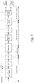
- FIG 1 shows an example of elements that may be included in a reception flow of a signal, in accordance with aspects of the disclosure.
- a signal (1) e.g. in Intermediate Frequency (IF)
- I/Q Demodulator (2) which may be configured to convert the signal to a baseband complex signal (3).
- Baseband signal (3) may be then presented at the input of an antialiasing low pass filter (LPF) (4) which may be configured to filter the baseband signal before it may be sampled by analog to digital converter (ADC) (5), wherein said sampling may transform the received signal to a digital complex representation.
- LPF antialiasing low pass filter
- ADC analog to digital converter
- said sampling may transform the received signal to a digital complex representation.
- said sampling may be performed using sampling frequency f s .
- the digital signal present at the output of ADC (5) may be presented at the input of re-sampler (6), which may be configured to resample the signal in accordance with at least a symbol rate property of the received signal (Rs), for example in order to provide Ns samples per symbol (wherein Ns>1 may be useful since an optimal sampling timing of a symbol may be initially unknown).
- the resampled complex sample stream at a sampling rate of Ns ⁇ Rs, may be presented at the input of matched filter (7), which may be configured to maximize the signal to noise ratio (SNR) and to provide its output signal at the same sampling rate as its input signal (e.g. Ns ⁇ Rs).
- the output signal of matched filter (7) may be presented at the input of automatic gain control (AGC) block (8), which may be configured to adjust the amplitude of the signal for at least the purpose of providing a signal having a predefined level at the input of fast acquisition block (Fast ACQ) (10).
- AGC automatic gain control
- re-sampler (6), matched filter (7), AGC block (8), decimation block (9) and fast acquisitions block (10) may be implemented in a Field Programmable Gate Array (FPGA).
- FPGA Field Programmable Gate Array
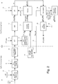
- Fig 2 shows an example block diagram of fast acquisition block (10) of Fig 1 .
- Samples, at rate of Na samples per symbol (12) may be presented at the input to the fast acquisition block and provided to UW modulation elimination block (11), an example description of which may be presented in Fig 3 .
- the complex input signal samples, sampled at Na ⁇ Rs (12) may be fed into two shift registers of length Na ⁇ L (e.g. shift register 28 for the I component and shift register 29 for the Q component).
- the samples may be backward rotated in accordance with the UW pattern (13 in Fig 2 ), wherein backward rotation may be performed by multiplying the input samples by an inversed pattern of the UW, as shown in Fig 3 .
- UW modulation elimination block (11) may be configured to present at its output a vector of L samples (elements) in length (i.e. the UW length), each sampled at Rs, every 1/(Na ⁇ Rs) time period. These vectors may represent un-modulated samples at intervals of 1/Rs.
- fast acquisition block (10) may be configured to include a samples counter (23), which may be configured to count the samples vectors coming out of UW modulation elimination block (11) (e.g. in accordance with a clock at a rate of Na ⁇ Rs) and associate each samples vector with an index.
- Samples counter (23) may be configured with modulo of Na ⁇ UWFL, hence each samples vector may have an initial arbitrary index within a UW frame (i.e. between 0 and Na ⁇ UWFL-1).
- samples counter 23 may be configured with modulo of 4000 (i.e. the count value may be ranging from 0 to 3999).
- a method for synchronizing samples counter (23) to a first symbol of a UW, so that sample counter (23) may show a predefined count value (for example, 0) at the same time that said first symbol of a UW may be valid at the input of fast acquisitions block (10).
- the output vectors of UW modulation elimination block (11) may optionally be passed through pre-summation block (14), having a configurable summation factor N.
- Pre-summation block (14) may optionally decimate groups of N adjacent samples by summing each group of N samples to form a single sample, at least for the purpose of reducing an input vector size of L samples to an output vector size of L/N samples.
- pre-summation with a factor being a power of 2 e.g. 2, 4, 8, 16, etc.
- An output vector of pre-summation (14), of length L/N, may be presented at the input of FFT (Fast Fourier Transform) module (16).
- FFT_size the size of the FFT input and output vectors
- detection resolution may remain unchanged since said pre-summation also reduces the effective sampling rate by the same ratio.
- FFT module (16) may be configured to compute a Fast Fourier Transform (FFT) of an input vector of a configurable size (e.g. FFT_size) and to output the transformed vector towards ABS block (17), as described further herein.
- FFT module (16) may be further configured to generate a second output, which may be used for driving FFT index counter (22), wherein FFT index counter (22) may be configured to count FFT output vector samples (i.e. FFT index counter may be configured with modulo of FFT_size).
- FFT module (16) may have one output which may be used both for providing transformed vectors to ABS block (17) and for driving FFT index counter (22).
- the output of FFT index counter (22) i.e.
- each FFT input/output vector may be already indexed using samples counter (23) (i.e. using the corresponding sample index for the FFT input vector), wherein samples counter (23) may be configured with modulo of Na ⁇ UWFL, as previously described.
- samples counter (23) i.e. its count value
- time_ind time axis index
- the pre-summation factor (N) may be determined at least in accordance with a ratio between a maximal frequency uncertainty (e.g. frequency offset or frequency error) a signal may be received at ( ⁇ F), and a symbol rate property of the received signal (Rs).
- the pre-summation factor (N) may be selected so that ⁇ F/Rs ⁇ 1/(4 ⁇ N) (i.e. the ratio between the signal's symbol rate and the maximal frequency uncertainty at which the signal may be received may be higher than 4 times the pre-summation factor).
- ⁇ F/Rs ⁇ 1/(4 ⁇ N) i.e. the ratio between the signal's symbol rate and the maximal frequency uncertainty at which the signal may be received may be higher than 4 times the pre-summation factor.
- said pre-summation factor may be used for adjusting an FFT vector size (FFT_size) to a desired size and/or for maintaining a constant maximal FFT processing rate over a range of input signals having a range of symbol rates.
- FFT_size an FFT vector size
- FFT module (16) may process L points' FFT at a rate of 2 ⁇ Na ⁇ Rs min .
- an overall processing rate of FFT module (16) may be maintained, at least for the purpose of facilitating an implementation of such FFT module.
- fast acquisitions block (10) may be implemented using a Field Programmable Gate Array (FPGA)
- the blocks preceding FFT module (16) may be operated at Na ⁇ Rs clock rate, while the rest of the functions, including perhaps FFT module (16), may be operated using a faster clock, at least for the purpose of supporting a required processing rate for FFT calculations.
- FPGA Field Programmable Gate Array
- the complex output vectors of FFT module (16) may be presented at the input of absolute value calculation (ABS) block (17), for at least the purpose of obtaining a metric of magnitude (also referred to herein as FFT amplitude).
- ABS block (17) may be implemented in many ways.
- the amplitude value of FFT results may be calculated, for example by using the following approximation: I + jQ ⁇ MAX ABS I , ABS Q + 1 ⁇ 2 MIN ABS I , ABS Q
- metrics of magnitude may include the absolute value of the amplitude, a square power of the amplitude, or any other monotonic function over amplitude.
- the received signal may be of low signal to noise ratio (SNR)
- SNR signal to noise ratio
- multiple FFT amplitude values which may be calculated by ABS block (17) for multiple UW frames (i.e. consecutive values may refer to samples which may be UWFL symbols apart), may be averaged for at least the purpose of increasing the probability for correctly determining the UW timing.
- averaging of FFT amplitudes for all possible time and frequency indexes may be done using Infinite Impulse Response filter (IIR) (18).
- IIR Infinite Impulse Response filter
- IIR filtering may be done by reading a previous IIR state from a memory (20), updating the IIR with the current FFT amplitude value (e.g. inp_data), and storing the result (H) back into memory (20).
- IIR filter (18) output values may be stored in memory (20), which may be configured to be of sufficient size for storing FFT_size ⁇ Na ⁇ UWFL values representing all time-frequency hypothesizes, wherein each value requires a single storage address.
- An address generation block (21) may be used for generating addresses for accessing memory (20), wherein each address may be composed of a least significant part representing a frequency index (FFT_ind) and a most significant part representing a timing index (Time_ind).
- a value stored in memory (20) during a previous iteration may be read and used together with a current FFT cell amplitude value (inp_data from ABS block (17)) for calculating a new IIR (18) value.
- the resulting IIR new value may then be stored in memory (20) at the same address holding the IIR result value of the previous iteration (prev val).
- IIR filter for averaging amplitude results is merely an example for such averaging.
- Other averaging methods may be used without leaving the scope of this disclosure, including for example any of summation, a sliding window, or use of Finite Impulse Response (FIR) filters.
- FIR Finite Impulse Response
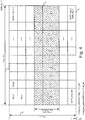
- FIG 4 shows an example of memory (20) organization and addressing (40).
- a frequency search range (41) may be set in accordance with a maximal possible frequency uncertainty (e.g. offset or error) that may be expected ( ⁇ F).
- the FFT frequency range may be larger than the maximal possible frequency error, for example the FFT frequency range may be ⁇ (Rs/(2 ⁇ N)) while only part of the FFT cells may be of interest.
- the expected maximal frequency uncertainty e.g. offset or error
- the number of FFT cells of interest may be only about half of the resulting FFT cell.
- the memory size of interest may be in the order of Na ⁇ UWFL ⁇ FFT_size/2.
- memory (20) may be reduced in size to hold only the cells of interest, wherein non-interesting results may be discarded.
- Memory (20) may be visualized as a two-dimensional histogram of timing and frequency offset hypothesis, as shown in Fig 4 .
- memory (20) may be a single dimension vector and said two-dimensional view may be obtained through having a frequency index (42) (FFT_ind), which may be used for driving the least significant bits (LSB) of the address, and a timing index (43) (Time_ind), which may be used for driving the most significant bits (MSB) of the address.
- FFT_ind frequency index
- time_ind timing index
- the address may include LOG 2 (Na ⁇ UWFL ⁇ FFT_size) bits, denoting the time-frequency cell address (for instance, the least significant address bits may be used for FFT bin index, while most significant address bits may denote the half-symbol location of the FFT input vector within samples counter (23) range).
- IIR memory (20) may be initially filled with zeroes (0).
- the leakage factor (K) may be set in accordance with a number of iterations that may be sufficient for obtaining a reliable acquisition decision, wherein 1/K may approximately be the said number of iterations.
- the memory location of a maximal amplitude level may be tracked. After a sufficient number of iterations, an index to the maximal amplitude level within memory (20) may indicate the frequency offset and the UW Frame timing index for the received signal.
- max search block (19) may be configured to provide an index to a maximal value (referred to herein as max index), corresponding to a chosen time-frequency hypothesis.
- the least significant portion of said max index may be used for frequency error estimation (Frequency Estimation block (24), while the most significant portion of said max index may be used as frame start time estimation (Time_est (31)) and possibly applied to samples counter (23) for at least the purpose of synchronizing samples counter (23) with the frame timing.
- the averaging factor (e.g. dictated by K in the IIR equation) may be configurable. In some embodiments, the averaging factor may be selected in accordance with specific SNR conditions. Maximum peak searching may be performed "on the fly", i.e. with each new index of IIR memory (20) being updated. Maximum search block (19) may be configured to provide any of the following on its outputs: a maximum peak value (maxvalue), a maximum peak time (Time_est) and a frequency index (FFT_ind).
- a lock detection decision ( Fig 2 , 25) may be conditioned to the maximum averaged amplitude value determined by max search (19) being higher than a threshold (32) (i.e. MAX(H) > Thr).
- a threshold i.e. MAX(H) > Thr.
- AGC (8) may be included in the demodulation chain, at least for the purpose of regulating a power level property of the received signal at the input to fast acquisition module (10) and/or allowing reliable lock detection using threshold (32) independently of the power level of the received signal at the input of the demodulation path.
- frequency error and frame timing estimates may become valid immediately after lock detection may be provided by lock detection block (25).
- the threshold value (32) (Thr) may be either predefined or configurable, and it may depend on any of a required acquisition detection probability, a false detection probability and said IIR leakage factor (33).
- determining termination of the acquisition process e.g. lock detection
- a transmission may include a single frame having a single UW.
- the UW timing within an uncertainty time window may be determined in parallel to determining a frequency offset at which the burst may be received.
- burst reception may not allow averaging of a metric of magnitude as previously described, as the UW may appear only once.
- burst timing and frequency offset may be determined by a maximal value of a metric of magnitude in the two-dimensional time-frequency map corresponding to a time-frequency search window.
- the methods described above may be used in a satellite communication system.
- a receiver configured to receive a signal from a satellite may be configured to use one or more of the methods described above at least for the purpose of acquiring frame timing (e.g. of a UW located within a frame) of a received signal wherein the signal may be received with frequency uncertainty.
- aspects of the disclosure may be embodied as one or more methods, systems, apparatuses (e.g., components of a satellite communication network), and/or computer program products. Accordingly, those aspects may take the form of an entirely hardware embodiment, an entirely software embodiment, an entirely firmware embodiment, or an embodiment combining firmware, software, and/or hardware aspects. Furthermore, such aspects may take the form of a computer program product stored by one or more computer-readable storage media having computer-readable program code, or instructions, embodied in or on the storage media. Any suitable computer readable storage media may be utilized, including hard disks, CD-ROMs, optical storage devices, magnetic storage devices, and/or any combination thereof. In some embodiments, one or more computer readable media storing instructions may be used.
- the instructions when executed, may cause one or more apparatuses to perform one or more acts described herein.
- the one or more computer readable media may comprise transitory and/or non-transitory media.
- various signals representing data or events as described herein may be transferred between a source and a destination in the form of electromagnetic waves traveling through signal-conducting media such as metal wires, optical fibers, and/or wireless transmission media (e.g., air and/or space).
Landscapes
- Engineering & Computer Science (AREA)
- Computer Networks & Wireless Communication (AREA)
- Signal Processing (AREA)
- Synchronisation In Digital Transmission Systems (AREA)
- Mobile Radio Communication Systems (AREA)
- Circuits Of Receivers In General (AREA)
Description
- Aspects of the disclosure pertain to the general field of communication modems. Aspects of the disclosure pertain to communication modems for wireless communication and satellite communication.
- Modern digital signals, for example over satellite links, may include some kind of framing. Framing may be needed, for instance, in order to determine an end of one code word (e.g. a data frame) and a start of a next code word (e.g. a next data frame) within the transmission. A known sequence of transmission symbols, which may be sometimes referred to as Unique Word (UW), may be used for framing synchronization. For example, in burst transmissions, a single UW (e.g. at the beginning of the burst) may be used for synchronizing the burst framing. In another example, in continuous transmission, a UW sequence may be occasionally transmitted, though for simplifying synchronization UW instances may be periodically transmitted, e.g. at constant intervals or distances (for example measured in symbols).
- A UW sequence may be detected using a coherent correlator. The correlator may rotate the known symbols of the UW "backwards", so that all the UW symbols may be added coherently (i.e. in phase). In some examples, if the phase of the received signal is unknown, an amplitude detector or a power detector may be used at the output of the correlator for detecting the UW existence. However, if a transmitted signal is received at some frequency offset, the UW symbols may be undesirably rotated while being added by a correlator (i.e. due to the frequency offset), causing the said addition of symbols to be at least somewhat incoherent. Thus, this undesired rotation may introduce degradation to the coherent detection, and in severe cases it may prevent detection of the UW. For example, if the transmission symbol rate is denoted as Rs, the UW length in symbols is denoted as L, and the frequency error is denoted as ΔF, a degradation in detection performance (in dB) may be calculated as:


- For example, at a frequency offset of Rs/(4L), the resulting degradation in detection performance might be in the excess of 1dB. In another example, at a frequency offset of Rs/L, detection might be entirely impossible (e.g. as ΔF aims to Rs/L, the expression SINC(L∗AF/Rs) aims to 0 and the expression 20LOG(SINC(L∗ΔF/Rs)) aims to minus infinity, i.e. the degradation at such a frequency offset might exceed the detector capabilities).
- Therefore, when trying to determine reception timing of a UW in presence of a relatively large frequency error, a receiver may use one or more techniques in order to enable detection of the UW. One technique is to determine the frequency offset through frequency scanning. The receiver may be set to receive the signal at a certain frequency and to try locating the UW. If the UW is not detected, the receiver frequency may be modified to a close neighbor frequency within a preconfigured frequency offset range, where the receiver may try again to locate the UW, and so on until the UW is located or the entire preconfigured frequency offset range may be scanned. However, this scanning method may significantly increase the acquisition time (e.g. the time it may take to synchronize or to lock the receiver on the received signal). It may be noted that if a frequency step size is in the order of Rs/2L, the residual maximal frequency error is Rs/4L, hence ensuring up to 1dB degradation in detection performance. However, selecting a frequency step size in the order of Rs/2L may imply a relatively large number of frequency steps (e.g. scanning iterations) that may be required before a correct frequency offset may be found.
- An alternative method to deal with frequency offset may be to divide the UW correlator into short segments, i.e. to perform the correlation in parts, so that any exiting frequency offset may result in smaller loss of coherency within each segment. The correlation results of all segments may then be further assembled in a non-coherent manner. For example, the amplitude-square of each segment correlation output may be computed and the results from all segments may be then combined. However, a disadvantage of this method may be its use of non-linear operation (e.g. such as squaring) before all fragment contributions may be added. This non-linear operation may introduce another source of detection-loss, often denoted as "Squaring Loss" that may become quite significant, for example in negative SNR (Signal to Noise Ratio) scenarios. The SNR at an output of a short-segment correlation of length m (SNRsegment_out) may be represented as:


- The squaring loss may be significantly increased as SNRsegment_out becomes more negative (e.g. Squaring_Loss ≈ -SNRsegment_out for negative SNRsegment_out values and at least 3dB for positive or high SNRsegment_out values). Thus, considering the above example:

- However, if the frequency offset is negligible, a full correlation may be calculated without segmentation. In such case:

- Thus, a more efficient technique for synchronizing to a signal framing under a significant frequency offset error may be useful. Such a technique should be fast on one hand and resulting in no or little degradation to detection performance on the other hand.
-
WO 99/20023 -
US 2004/0218699 discloses detecting a message identifier or preamble that has been generated and provided by a transmitter 200 that uses FFTs to estimate frequency and time offset. The wireless receiver 300 scans, asynchronously and sequentially during a wakeup time, a plurality of predetermined frequencies for the message identifier or specialized preamble. A plurality of received sample sequences are collected, one received sample sequence collected at each of the plurality of predetermined frequencies. A correlation between data corresponding to the preamble and data corresponding to a received sample sequence is compared to a threshold value to determine when the preamble has been detected. The wireless receiver 300 is wakened from a low power mode when the preamble is detected. - The present invention is defined in its method aspect in
claim 1 and in its system aspect inclaim 11. The following presents a simplified summary in order to provide a basic understanding of some aspects of the disclosure. The summary is not an extensive overview of the disclosure. It is neither intended to identify key or critical elements of the disclosure nor to delineate the scope of the disclosure. The following summary merely presents some aspects of the disclosure in a simplified form as a prelude to the description below. - Aspects of the disclosure are directed to a method for fast acquisition of symbol and/or frame timing of a signal, which may be received with frequency uncertainty. In some embodiments, the method may include steps of Unique Word (UW) modulation elimination, optional partial coherent addition and Fourier Transform (FT) processing, and a two-dimensional search of UW timing and/or of frequency offset. Such method may be useful for speeding timing acquisition of a framed signal, including in the presence of a frequency uncertainty or offset.
- Aspects of the disclosure are directed to a receiver, which may be configured to use an algorithm for acquiring frame timing (e.g. UW location within a frame) in presence of frequency uncertainty. In some embodiments, the algorithm may be implemented using a Field Programmable Gate Array (FPGA).
- Having thus described the disclosure in general terms, reference will now be made to the accompanying drawings, which are not necessarily drawn to scale, and wherein:
-
Fig 1 shows a block diagram of a demodulation path in accordance with aspects of the disclosure. -
Fig 2 shows a block diagram of a fast acquisition function in accordance with aspects of the disclosure. -
Fig 3 shows a diagram of unique-word pattern elimination functionality in accordance with aspects of the disclosure. -
Fig 4 shows an example representation of a two-dimensional search map in accordance with aspects of the disclosure. - A receiver may be configured to receive a signal at a given frequency and to synchronize with a framing property of the received signal, wherein framing may be marked by a predefined sequence of symbols, known as Unique Word (UW). For the purpose of simplifying the disclosure description and for maintaining coherency of the examples given, let L represent the length in symbols of a UW (for example, L = 64) and let UWFL represent the length in symbols of a UW frame, i.e. the distance between adjacent UW instances, (for example UWFL = 2000). Given the above terminology, the methods disclosed herein may be directed at detecting the UW sequence (or pattern) within the UW frame, while there may be UWFL possible timings (i.e. locations on a time axis with a symbol period grid) and wherein said detection may be influenced by receiving the signal with a frequency uncertainty or at some frequency offset.
- Furthermore, for the sake of simplicity, reference may be made herein to use of the Fast Fourier Transform (FFT) algorithm for computing a Fourier Transform (FT). However, any other method or algorithm for computing a Fourier Transform (FT) may be used without leaving the scope of this disclosure and without changing any of its aspects.
-
Fig 1 shows an example of elements that may be included in a reception flow of a signal, in accordance with aspects of the disclosure. A signal (1) (e.g. in Intermediate Frequency (IF)) may be presented at the input of I/Q Demodulator (2), which may be configured to convert the signal to a baseband complex signal (3). Baseband signal (3) may be then presented at the input of an antialiasing low pass filter (LPF) (4) which may be configured to filter the baseband signal before it may be sampled by analog to digital converter (ADC) (5), wherein said sampling may transform the received signal to a digital complex representation. In some embodiments, said sampling may be performed using sampling frequency fs. - The digital signal present at the output of ADC (5), may be presented at the input of re-sampler (6), which may be configured to resample the signal in accordance with at least a symbol rate property of the received signal (Rs), for example in order to provide Ns samples per symbol (wherein Ns>1 may be useful since an optimal sampling timing of a symbol may be initially unknown). In some embodiments, re-sampler (6) may be configured to output the resampled signal using a sampling rate of 4Rs (where Rs is the signal's symbol rate), hence providing 4 samples per each symbol (i.e. Ns = 4). The resampled complex sample stream, at a sampling rate of Ns∗Rs, may be presented at the input of matched filter (7), which may be configured to maximize the signal to noise ratio (SNR) and to provide its output signal at the same sampling rate as its input signal (e.g. Ns∗Rs). The output signal of matched filter (7) may be presented at the input of automatic gain control (AGC) block (8), which may be configured to adjust the amplitude of the signal for at least the purpose of providing a signal having a predefined level at the input of fast acquisition block (Fast ACQ) (10). In some embodiments, fast acquisition block (10) may be configured to process the signal at a sampling rate of Na∗Rs (for example, Na = 2), thus an additional decimation block (9) of factor Ns/Na may be used before fast acquisition block (10) (for example, where Ns = 4 and Na = 2, a decimation factor of 2 may be used).
- In some embodiments, re-sampler (6), matched filter (7), AGC block (8), decimation block (9) and fast acquisitions block (10) may be implemented in a Field Programmable Gate Array (FPGA). However, other embodiments in which the above functions may be implemented either in hardware, firmware, software, any mix of hardware, firmware and software, or any other means for implementing such functions, may also be possible and are therefore envisaged by this disclosure.
-
Fig 2 shows an example block diagram of fast acquisition block (10) ofFig 1 . Samples, at rate of Na samples per symbol (12) may be presented at the input to the fast acquisition block and provided to UW modulation elimination block (11), an example description of which may be presented inFig 3 . The complex input signal samples, sampled at Na∗Rs (12), may be fed into two shift registers of length Na∗L (e.g. shift register 28 for the I component andshift register 29 for the Q component). The samples may be backward rotated in accordance with the UW pattern (13 inFig 2 ), wherein backward rotation may be performed by multiplying the input samples by an inversed pattern of the UW, as shown inFig 3 . In some embodiments, where the UW may be transmitted as a binary sequence, for example using BPSK modulation, elimination of the UW pattern may require multiplying the I and Q components (26 and 27 respectively) of the input signal by UW pattern (30) (for example, by 1 for a "1" bit and by -1 for a "0" bit). UW modulation elimination block (11) may be configured to present at its output a vector of L samples (elements) in length (i.e. the UW length), each sampled at Rs, every 1/(Na∗Rs) time period. These vectors may represent un-modulated samples at intervals of 1/Rs. - In parallel to processing the input samples, fast acquisition block (10) may be configured to include a samples counter (23), which may be configured to count the samples vectors coming out of UW modulation elimination block (11) (e.g. in accordance with a clock at a rate of Na∗Rs) and associate each samples vector with an index. Samples counter (23) may be configured with modulo of Na∗UWFL, hence each samples vector may have an initial arbitrary index within a UW frame (i.e. between 0 and Na∗UWFL-1). Following the above example, where Na = 2 and UWFL = 2000, samples counter 23 may be configured with modulo of 4000 (i.e. the count value may be ranging from 0 to 3999).
- In some aspects of the disclosure, a method is presented for synchronizing samples counter (23) to a first symbol of a UW, so that sample counter (23) may show a predefined count value (for example, 0) at the same time that said first symbol of a UW may be valid at the input of fast acquisitions block (10).
- Referring again to
Fig 2 , the output vectors of UW modulation elimination block (11) may optionally be passed through pre-summation block (14), having a configurable summation factor N. Pre-summation block (14) may optionally decimate groups of N adjacent samples by summing each group of N samples to form a single sample, at least for the purpose of reducing an input vector size of L samples to an output vector size of L/N samples. In one example, wherein the signal may be received at a relatively large frequency offset, pre-summation block (14) may be bypassed (i.e. N = 1, at least in order to avoid loss of SNR that may result from coherent addition of neighbor symbols). In another example, wherein a UW length may be L = 64, pre-summation with a factor being a power of 2 (e.g. 2, 4, 8, 16, etc.) may be used. An output vector of pre-summation (14), of length L/N, may be presented at the input of FFT (Fast Fourier Transform) module (16). Thus, the summation factor N may define the size of the FFT input and output vectors (FFT_size) and in some embodiments as described above it may reduce the vector size. Though reducing the FFT vector size may result in reducing the number of coefficients in the FFT input and output vectors, detection resolution may remain unchanged since said pre-summation also reduces the effective sampling rate by the same ratio. In order to improve detection performance and the FFT grid resolution, the FFT vector size is enlarged using time domain zero padding (15), thus providing at least a finer frequency resolution. In some embodiments, an FFT vector may be P∗(L/N) samples long, i.e. (L/N)∗(P-1) zeroes may be added to the L/N pre-summation samples (for example, a zero padding factor P=2 may be used). - FFT module (16) may be configured to compute a Fast Fourier Transform (FFT) of an input vector of a configurable size (e.g. FFT_size) and to output the transformed vector towards ABS block (17), as described further herein. FFT module (16) may be further configured to generate a second output, which may be used for driving FFT index counter (22), wherein FFT index counter (22) may be configured to count FFT output vector samples (i.e. FFT index counter may be configured with modulo of FFT_size). In some embodiments, FFT module (16) may have one output which may be used both for providing transformed vectors to ABS block (17) and for driving FFT index counter (22). In some embodiments, the output of FFT index counter (22) (i.e. its count value) may be used for providing at least a frequency axis index (FFT_ind) to address generation module (21). In addition, each FFT input/output vector may be already indexed using samples counter (23) (i.e. using the corresponding sample index for the FFT input vector), wherein samples counter (23) may be configured with modulo of Na∗UWFL, as previously described. In some embodiments, said the output of samples counter (23) (i.e. its count value) may be used for providing at least a time axis index (Time_ind) to address generation module (21).
- A summation operation may reduce an equivalent sampling rate of a signal presented at FFT module (16) input, for example to Rs/N, wherein Rs is the signal's symbol rate and N may be the pre-summation factor (
Fig 2 , 14). Consequently, FFT bin resolution (i.e. the frequency difference between neighboring FFT coefficients) may equal to (Rs/N)/((L/N)∗P) = Rs/(P∗L). The pre-summation factor (N) may be determined at least in accordance with a ratio between a maximal frequency uncertainty (e.g. frequency offset or frequency error) a signal may be received at (ΔF), and a symbol rate property of the received signal (Rs). In some embodiments, wherein said determining may be performed at least for the purpose of minimizing a degradation that may result from a pre-summation operation, the pre-summation factor (N) may be selected so that ΔF/Rs < 1/(4∗N) (i.e. the ratio between the signal's symbol rate and the maximal frequency uncertainty at which the signal may be received may be higher than 4 times the pre-summation factor). Thus, as the symbol rate of a received signal may be higher, a higher pre-summation factor may be used. In some embodiments, said pre-summation factor may be used for adjusting an FFT vector size (FFT_size) to a desired size and/or for maintaining a constant maximal FFT processing rate over a range of input signals having a range of symbol rates. For example, assuming that for a minimal symbol rate that a receiver may be configured to receive (Rsmin) a maximal FFT vector size may be set as FFT_size = P∗L (e.g. pre-summation might not be used in this case, i.e. N = 1). Consequently, FFT module (16) may process a 2∗L points' FFT (e.g. in case P = 2) at a rate of Na∗Rsmin. However, for a higher symbol rate, for example a symbol rate being twice the minimal symbol rate (i.e. 2∗Rsmin) and a zero-padding factor of P = 2, the pre-summation factor may be set to N = 2, resulting in FFT vector size of FFT_size = (L/N)∗2 = L. In other words, FFT module (16) may process L points' FFT at a rate of 2∗Na∗Rsmin. Thus, using such determining of the pre-summation factor, an overall processing rate of FFT module (16) may be maintained, at least for the purpose of facilitating an implementation of such FFT module. In some embodiments, where fast acquisitions block (10) may be implemented using a Field Programmable Gate Array (FPGA), the blocks preceding FFT module (16) may be operated at Na∗Rs clock rate, while the rest of the functions, including perhaps FFT module (16), may be operated using a faster clock, at least for the purpose of supporting a required processing rate for FFT calculations. - The complex output vectors of FFT module (16) may be presented at the input of absolute value calculation (ABS) block (17), for at least the purpose of obtaining a metric of magnitude (also referred to herein as FFT amplitude). ABS block (17) may be implemented in many ways. In some embodiments, the amplitude value of FFT results may be calculated, for example by using the following approximation:

- In some embodiments, other metrics of magnitude (i.e. other than FFT amplitude value), which are monotonic, may be used. For example, such metrics of magnitude may include the absolute value of the amplitude, a square power of the amplitude, or any other monotonic function over amplitude.
- In cases where the received signal may be of low signal to noise ratio (SNR), a single pass over all Na∗UWFL time hypothesis may be insufficient for accurately determining a UW timing. Consequently, multiple FFT amplitude values, which may be calculated by ABS block (17) for multiple UW frames (i.e. consecutive values may refer to samples which may be UWFL symbols apart), may be averaged for at least the purpose of increasing the probability for correctly determining the UW timing. After a first UW frame, averaging of FFT amplitudes for all possible time and frequency indexes may be done using Infinite Impulse Response filter (IIR) (18). IIR filtering may be done by reading a previous IIR state from a memory (20), updating the IIR with the current FFT amplitude value (e.g. inp_data), and storing the result (H) back into memory (20). IIR filter (18) output values may be stored in memory (20), which may be configured to be of sufficient size for storing FFT_size∗Na∗UWFL values representing all time-frequency hypothesizes, wherein each value requires a single storage address. An address generation block (21) may be used for generating addresses for accessing memory (20), wherein each address may be composed of a least significant part representing a frequency index (FFT_ind) and a most significant part representing a timing index (Time_ind). A value stored in memory (20) during a previous iteration (prev val) may be read and used together with a current FFT cell amplitude value (inp_data from ABS block (17)) for calculating a new IIR (18) value. The resulting IIR new value (next val) may then be stored in memory (20) at the same address holding the IIR result value of the previous iteration (prev val).
- It should be noted that use of an IIR filter for averaging amplitude results is merely an example for such averaging. Other averaging methods may be used without leaving the scope of this disclosure, including for example any of summation, a sliding window, or use of Finite Impulse Response (FIR) filters.
-
FIG 4 shows an example of memory (20) organization and addressing (40). A frequency search range (41) may be set in accordance with a maximal possible frequency uncertainty (e.g. offset or error) that may be expected (ΔF). It may be noted that the FFT frequency range may be larger than the maximal possible frequency error, for example the FFT frequency range may be ±(Rs/(2∗N)) while only part of the FFT cells may be of interest. For example, where the expected maximal frequency uncertainty (e.g. offset or error) may be ±Rs/4 and wherein N=1 (i.e. pre-summation may be bypassed), the number of FFT cells of interest may be only about half of the resulting FFT cell. Consequently, in the above example, the memory size of interest may be in the order of Na∗UWFL∗FFT_size/2. In such embodiments, memory (20) may be reduced in size to hold only the cells of interest, wherein non-interesting results may be discarded. - Memory (20) may be visualized as a two-dimensional histogram of timing and frequency offset hypothesis, as shown in
Fig 4 . In some embodiments, where fast acquisitions block (10) may be implemented in an FPGA, memory (20) may be a single dimension vector and said two-dimensional view may be obtained through having a frequency index (42) (FFT_ind), which may be used for driving the least significant bits (LSB) of the address, and a timing index (43) (Time_ind), which may be used for driving the most significant bits (MSB) of the address. It may be noted that in the worst case (i.e. wherein memory (20) may be configured to hold all the FFT results of FFT module (16)), the address may include LOG2(Na∗UWFL∗FFT_size) bits, denoting the time-frequency cell address (for instance, the least significant address bits may be used for FFT bin index, while most significant address bits may denote the half-symbol location of the FFT input vector within samples counter (23) range). - Again in reference to
Fig 2 , in some embodiments IIR memory (20) may be initially filled with zeroes (0). The IIR filter (18) output, H(n), may be calculated from input X(n) using the equation:
- In parallel to updating IIR memory (20), the memory location of a maximal amplitude level may be tracked. After a sufficient number of iterations, an index to the maximal amplitude level within memory (20) may indicate the frequency offset and the UW Frame timing index for the received signal.
- Again in reference to
Fig 2 , in order to estimate a cell holding a value representing maximal power, calculation results from IIR (18) may be streamed to max search block (19), which may be configured to provide an index to a maximal value (referred to herein as max index), corresponding to a chosen time-frequency hypothesis. The least significant portion of said max index may be used for frequency error estimation (Frequency Estimation block (24), while the most significant portion of said max index may be used as frame start time estimation (Time_est (31)) and possibly applied to samples counter (23) for at least the purpose of synchronizing samples counter (23) with the frame timing. - The averaging factor (e.g. dictated by K in the IIR equation) may be configurable. In some embodiments, the averaging factor may be selected in accordance with specific SNR conditions. Maximum peak searching may be performed "on the fly", i.e. with each new index of IIR memory (20) being updated. Maximum search block (19) may be configured to provide any of the following on its outputs: a maximum peak value (maxvalue), a maximum peak time (Time_est) and a frequency index (FFT_ind).
- A lock detection decision (
Fig 2 , 25) may be conditioned to the maximum averaged amplitude value determined by max search (19) being higher than a threshold (32) (i.e. MAX(H) > Thr). Referring toFig 1 , in some embodiments an automatic gain control block, AGC (8), may be included in the demodulation chain, at least for the purpose of regulating a power level property of the received signal at the input to fast acquisition module (10) and/or allowing reliable lock detection using threshold (32) independently of the power level of the received signal at the input of the demodulation path. - In some embodiments, frequency error and frame timing estimates may become valid immediately after lock detection may be provided by lock detection block (25). The threshold value (32) (Thr) may be either predefined or configurable, and it may depend on any of a required acquisition detection probability, a false detection probability and said IIR leakage factor (33). In some embodiments, determining termination of the acquisition process (e.g. lock detection) may be based on using a first maximum and a second maximum peak ratio compared to a threshold, wherein said second maximum peak might not be associated with a nearest neighbor in either time or frequency to said first maximum peak.
- In some embodiments, wherein the processed signal may be a burst signal, a transmission may include a single frame having a single UW. In such embodiments, the UW timing within an uncertainty time window may be determined in parallel to determining a frequency offset at which the burst may be received. In addition, burst reception may not allow averaging of a metric of magnitude as previously described, as the UW may appear only once. Thus, burst timing and frequency offset may be determined by a maximal value of a metric of magnitude in the two-dimensional time-frequency map corresponding to a time-frequency search window.
- In some embodiments, the methods described above may be used in a satellite communication system. A receiver configured to receive a signal from a satellite may be configured to use one or more of the methods described above at least for the purpose of acquiring frame timing (e.g. of a UW located within a frame) of a received signal wherein the signal may be received with frequency uncertainty.
- Various aspects of the disclosure may be embodied as one or more methods, systems, apparatuses (e.g., components of a satellite communication network), and/or computer program products. Accordingly, those aspects may take the form of an entirely hardware embodiment, an entirely software embodiment, an entirely firmware embodiment, or an embodiment combining firmware, software, and/or hardware aspects. Furthermore, such aspects may take the form of a computer program product stored by one or more computer-readable storage media having computer-readable program code, or instructions, embodied in or on the storage media. Any suitable computer readable storage media may be utilized, including hard disks, CD-ROMs, optical storage devices, magnetic storage devices, and/or any combination thereof. In some embodiments, one or more computer readable media storing instructions may be used. The instructions, when executed, may cause one or more apparatuses to perform one or more acts described herein. The one or more computer readable media may comprise transitory and/or non-transitory media. In addition, various signals representing data or events as described herein may be transferred between a source and a destination in the form of electromagnetic waves traveling through signal-conducting media such as metal wires, optical fibers, and/or wireless transmission media (e.g., air and/or space).
- Modifications may be made to the various embodiments described herein by those skilled in the art. It will also be appreciated and understood that modifications may be made without departing from the scope of the present disclosure. The description is thus to be regarded as illustrative instead of restrictive on the present disclosure.
Claims (15)
- A method including:receiving a modulated signal comprising a framing property marked by a unique word comprising a predefined sequence of symbols;producing a digitally sampled signal corresponding to the modulated signal, the digitally sampled signal having a sampling rate of Na ∗ Rs, wherein Rs is a symbol rate of the modulated signal and Na is a number of samples per symbol;determining a frequency offset associated with the modulated signal and a location of the unique word within a frame of the modulated signal, wherein the determining is based on a two-dimensional search in a time-frequency map and wherein the determining comprises:a.) eliminating a unique word modulation from the digitally sampled signal to produce a plurality of vectors each having L un-modulated samples at intervals of 1/Rs, wherein L is a length, in symbols, of the unique word;b.) counting the plurality of vectors using a first counter and associating each of the plurality of vectors with a time index corresponding to a count value of the first counter;c.) summing groups of N adjacent samples within each of the plurality of vectors to produce decimated vectors of L/N samples, wherein N is a positive integer;d.) padding the decimated vectors with time-domain zeroes to produce padded vectors of P∗(L/N) samples, wherein P ≥ 1;e.) performing a Fourier Transform, FT, on the padded vectors to produce transformed vectors;f.) counting FT samples of the transformed vectors using a second counter and associating each of the FT samples with a frequency index corresponding to a count value of the second counter;g.) calculating at least one metric of magnitude for each sample in the transformed vectors; andh.) storing the at least one metric of magnitude at a storage address in a memory, wherein the storage address is determined in accordance with the time index and the frequency index associated with a sample corresponding to the at least one metric of magnitude.
- The method of claim 1, wherein producing the digitally sampled signal comprises:demodulating the modulated signal to produce a complex baseband signal;converting the complex baseband signal to a digitally sampled complex signal;filtering the digitally sampled complex signal using a matched filter to produce a matched filter output signal; anddecimating the matched filter output signal to produce the digitally sampled signal having the sampling rate of Na ∗ Rs.
- The method of claim 1, wherein calculating the at least one metric of magnitude comprises averaging results that are UWFL symbols apart, wherein UWFL is a distance, in symbols, between adjacent instances of the unique word, wherein the averaging is performed through filtering the at least one metric of magnitude using an Infinite Impulse Response, IIR, filter and wherein the filtering comprises:reading a previously stored value, H(n-1), from the storage address of the memory;calculating an IIR filter output value, H(n), in accordance with the following expression: H(n) = K∗X(n) + (1-K)∗H(n-1), wherein K is a leakage factor value and X(n) corresponds to a value of a sample presented at an input of the IIR filter; andstoring the calculated IIR filter output value, H(n), in the memory at the storage address.
- The method of claim 1, further comprising determining of the storage address in accordance with the time index and the frequency index by using the frequency index to form a first portion of bits of the storage address and using the time index to form a second portion of bits of the storage address.
- The method of claim 1, further comprising setting N equal to 1 to reduce effects of the summing of the groups of N adjacent samples.
- The method of claim 1, further comprising determining N in accordance with a ratio between a maximal frequency uncertainty, ΔF, and the symbol rate, Rs, of the modulated signal.
- The method of claim 1, further comprising:providing values, H, stored in memory for a maximum search in parallel to storing the values in the memory;determining a maximal value, MAX(H), of the provided values;comparing the maximum value with a threshold, Thr; anddetermining a lock on the modulated signal if the maximum value is greater than the threshold, MAX(H) > Thr, wherein determining a lock on the modulated signal comprises:determining a first maximum value from a plurality of values stored in the memory, the first maximum value corresponding to a first time index and a first frequency index;determining a second maximum value from the plurality of values stored in the memory, the second maximum value corresponding to a second time index and a second frequency index, wherein the second time index is not a nearest neighbor of the first time index and the second frequency index is not a nearest neighbor of the first frequency index;calculating a ratio between the first maximum value and the second maximum value;comparing the calculated ratio to a threshold; anddetermining the lock on the modulated signal if the ratio exceeds the threshold.
- The method of claim 1, further comprising:providing values, H, stored in memory for a maximum search in parallel to storing the values in the memory;determining a maximal value, MAX(H), of the provided values;comparing the maximum value with a threshold, Thr,determining a lock on the modulated signal if the maximum value is greater than the threshold, MAX(H) > Thr;determining a maximum index corresponding to the determined maximal value when the lock is determined;determining a frequency offset of the modulated signal using a first portion of the maximum index; anddetermining a frame start time estimation using a second portion of the maximum index, wherein the frame start time estimation is used for synchronizing the first counter with frame timing.
- The method of claim 1, wherein the eliminating the unique word modulation comprises:
backward rotating the digitally sampled signal. - The method of claim 1, wherein the eliminating the unique word modulation comprises:
multiplying I and Q components of the digitally sampled signal by the UW. - A system, comprising:memory; anda receiver coupled to the memory, the receiver configured to:receive a modulated signal (1) comprising a framing property marked by a unique word comprising a predefined sequence of symbols;produce a digitally sampled signal (12) corresponding to the modulated signal, the digitally sampled signal having a sampling rate of Na ∗ Rs, wherein Rs is a symbol rate of the modulated signal and Na is a number of samples per symbol;determine (10) a frequency offset associated with the modulated signal and a location of the unique word within a frame of the modulated signal, wherein the determining is based on a search in a time-frequency search window and wherein the determining comprises:a.) eliminating a unique word modulation (11) from the digitally sampled signal (12) to produce a plurality of vectors each having L un-modulated samples at intervals of 1/Rs, wherein L is a length, in symbols, of the unique word;b.) counting the plurality of vectors using a first counter (23) and associating each of the plurality of vectors with a time index corresponding to a count value of the first counter;c.) summing groups of N adjacent samples within each of the plurality of vectors (14) to produce decimated vectors of L/N samples, wherein N is a positive integer;d.) padding the decimated vectors (15) with time-domain zeroes to produce padded vectors of P∗(L/N) samples, wherein P ≥ 1;e.) performing a Fourier Transform, FT, (16) on the padded vectors to produce transformed vectors;f.) counting FT samples of the transformed vectors using a second counter (22) and associating each of the FT samples with a frequency index corresponding to a count value of the second counter;g.) calculating at least one metric of magnitude (17) for each sample in the transformed vectors; andh.) storing the at least one metric of magnitude at a storage address in the memory (20), wherein the storage address is determined in accordance with the time index and the frequency index associated with a sample corresponding to the at least one metric of magnitude.
- The system of claim 11, wherein the receiver comprises:a demodulator (2) configured for demodulating the modulated signal and producing a complex baseband signal (3);an analog to digital converter (5) configured for converting the complex baseband signal to a digitally sampled complex signal at a sampling rate of fs;a re-sampler (6) configured for resampling the digitally sampled complex signal at a sampling rate of Ns ∗ Rs to produce a resampled complex signal, wherein Ns is a number of samples per symbol;a matched filter (7) configured for filtering the resampled complex signal to produce a matched filter output signal; anda decimator (9) configured for decimating the matched filter output signal to produce the digitally sampled signal having the sampling rate of Na ∗ Rs.
- The system of claim 11, wherein the receiver comprises:an Infinite Impulse Response, IIR, filter (18) configured for averaging metric of magnitude values using a leakage factor (33),wherein the receiver is further configured to store the averaged metric of magnitude values in the memory (20), wherein a storage address for each value of the averaged metric of magnitude values is determined in accordance with a time index and a frequency index associated with a sample corresponding to the value.
- The system of claim 11, wherein the receiver is configured to receive signals transmitted from a satellite.
- The system of claim 12,wherein the re-sampler, the matched filter, and the decimator are implemented using one or more Field Programmable Gate Array, FPGA, devices, andwherein the one or more FPGA devices are used for determining the frequency offset associated with the modulated signal and the location of the unique word within the frame of the modulated signal.
Applications Claiming Priority (2)
| Application Number | Priority Date | Filing Date | Title |
|---|---|---|---|
| US201261585389P | 2012-01-11 | 2012-01-11 | |
| US13/668,788 US8804878B2 (en) | 2012-01-11 | 2012-11-05 | Fast acquisition of frame timing and frequency |
Publications (3)
| Publication Number | Publication Date |
|---|---|
| EP2615770A2 EP2615770A2 (en) | 2013-07-17 |
| EP2615770A3 EP2615770A3 (en) | 2014-11-05 |
| EP2615770B1 true EP2615770B1 (en) | 2020-06-17 |
Family
ID=47358351
Family Applications (1)
| Application Number | Title | Priority Date | Filing Date |
|---|---|---|---|
| EP12192244.7A Active EP2615770B1 (en) | 2012-01-11 | 2012-11-12 | Fast acquisition of frame timing and frequency |
Country Status (2)
| Country | Link |
|---|---|
| US (1) | US8804878B2 (en) |
| EP (1) | EP2615770B1 (en) |
Families Citing this family (9)
| Publication number | Priority date | Publication date | Assignee | Title |
|---|---|---|---|---|
| US10305578B2 (en) | 2014-05-14 | 2019-05-28 | Satixfy Israel Ltd. | Method of exchanging communications between a satellite and terminals associated therewith |
| US10368327B2 (en) * | 2014-05-14 | 2019-07-30 | Satixfy Israel Ltd. | Method and system for signal communications |
| US10033509B2 (en) | 2014-05-20 | 2018-07-24 | Satixfy Israel Ltd. | Method and system for satellite communication |
| CN106537788B (en) | 2014-05-20 | 2019-09-03 | 萨迪斯飞以色列有限公司 | Method for reducing interference in a satellite communication network |
| TW201931813A (en) * | 2018-01-09 | 2019-08-01 | 財團法人資訊工業策進會 | Wireless communication device and time and frequency synchronization method and non-transitory computer readable medium of the same |
| WO2021124329A1 (en) * | 2019-12-17 | 2021-06-24 | E.Q. Earthquake Ltd. | Systems and methods for earthquake detection and alerts |
| US12273848B2 (en) * | 2019-12-31 | 2025-04-08 | Deeyook Location Technologies Ltd | Interferometric location sensing |
| US12047205B2 (en) * | 2020-04-28 | 2024-07-23 | Lg Electronics Inc. | Signal processing device and image display apparatus including the same |
| US12149938B2 (en) * | 2020-06-15 | 2024-11-19 | Cisco Technology, Inc. | Dynamically encrypted radio frequency fingerprinting |
Family Cites Families (6)
| Publication number | Priority date | Publication date | Assignee | Title |
|---|---|---|---|---|
| DE4130864C2 (en) * | 1991-09-17 | 1999-04-15 | Daimler Benz Aerospace Ag | Digital messaging system |
| US5383225A (en) * | 1992-12-17 | 1995-01-17 | Motorola, Inc. | Synchronizer for TDMA acquisition signal having an unknown frequency |
| US6134286A (en) * | 1997-10-14 | 2000-10-17 | Ericsson Inc. | Synchronization techniques and systems for radiocommunication |
| US7106814B2 (en) * | 2003-04-30 | 2006-09-12 | Motorola, Inc. | Method and wireless device employing a preamble to initiate communications |
| KR100800692B1 (en) * | 2005-04-11 | 2008-02-01 | 삼성전자주식회사 | Frequency offset estimator and method for orthogonal frequency division multiplexing system |
| CA2656976C (en) * | 2006-07-07 | 2012-03-20 | Lg Electronics Inc. | Digital broadcasting system and method of processing data |
-
2012
- 2012-11-05 US US13/668,788 patent/US8804878B2/en active Active
- 2012-11-12 EP EP12192244.7A patent/EP2615770B1/en active Active
Non-Patent Citations (1)
| Title |
|---|
| None * |
Also Published As
| Publication number | Publication date |
|---|---|
| US8804878B2 (en) | 2014-08-12 |
| EP2615770A3 (en) | 2014-11-05 |
| US20130177061A1 (en) | 2013-07-11 |
| EP2615770A2 (en) | 2013-07-17 |
Similar Documents
| Publication | Publication Date | Title |
|---|---|---|
| US8804878B2 (en) | Fast acquisition of frame timing and frequency | |
| KR100770924B1 (en) | Frequency Error Compensation Device and Method in Wireless Communication System | |
| KR100377257B1 (en) | Method and apparatus for fine frequency synchronization in multi-carrier demodulation systems | |
| US9071327B2 (en) | Efficient frequency estimation | |
| US6134286A (en) | Synchronization techniques and systems for radiocommunication | |
| US10868705B2 (en) | Transmitter and receiver and corresponding methods | |
| KR102341875B1 (en) | Transmitter and receiver and methods thereof | |
| US12206526B2 (en) | System and method for blind channel estimation and coherent differential equalization in an orthogonal frequency division multiplexing (OFDM) receiver | |
| US8995576B2 (en) | Method and module for estimating frequency bias in a digital-telecommunications system | |
| CN113132285A (en) | Digital demodulation system and method | |
| KR20130104289A (en) | Apparatus and method for estimating offset value, receiving apparatus, and method for processing signal in the same | |
| CN112953593A (en) | LoRa advanced receiver | |
| US7620125B1 (en) | Frequency estimation apparatus and related method | |
| US7583770B2 (en) | Multiplex signal error correction method and device | |
| RU2396724C2 (en) | Methods and device for detection of time connection in system of wireless communication | |
| US6662000B1 (en) | Synchronisation method and device for a communication receiver | |
| JP4044022B2 (en) | MFSK reception system | |
| US9059835B1 (en) | Method and apparatus for demodulating a wireless signal | |
| CN115632923B (en) | OQPSK-based unmanned aerial vehicle and satellite ultra-wideband communication method and related equipment | |
| JP2021082984A (en) | Autocorrelator and receiver | |
| CN117768282A (en) | MSK signal demodulation method, terminal equipment and storage medium | |
| Herzet | Code-aided synchronization for digital burst communications. | |
| US9094266B2 (en) | Efficient de-spreading | |
| CN116389210A (en) | Blind Estimation Method, System and Medium of FSK Carrier Frequency Offset Based on L&R Algorithm | |
| JP4842172B2 (en) | Spread spectrum receiver |
Legal Events
| Date | Code | Title | Description |
|---|---|---|---|
| PUAI | Public reference made under article 153(3) epc to a published international application that has entered the european phase |
Free format text: ORIGINAL CODE: 0009012 |
|
| AK | Designated contracting states |
Kind code of ref document: A2 Designated state(s): AL AT BE BG CH CY CZ DE DK EE ES FI FR GB GR HR HU IE IS IT LI LT LU LV MC MK MT NL NO PL PT RO RS SE SI SK SM TR |
|
| AX | Request for extension of the european patent |
Extension state: BA ME |
|
| RAP1 | Party data changed (applicant data changed or rights of an application transferred) |
Owner name: GILAT SATELLITE NETWORKS LTD. |
|
| PUAL | Search report despatched |
Free format text: ORIGINAL CODE: 0009013 |
|
| AK | Designated contracting states |
Kind code of ref document: A3 Designated state(s): AL AT BE BG CH CY CZ DE DK EE ES FI FR GB GR HR HU IE IS IT LI LT LU LV MC MK MT NL NO PL PT RO RS SE SI SK SM TR |
|
| AX | Request for extension of the european patent |
Extension state: BA ME |
|
| RIC1 | Information provided on ipc code assigned before grant |
Ipc: H04L 7/04 20060101AFI20141001BHEP Ipc: H04B 7/185 20060101ALN20141001BHEP Ipc: H04L 27/00 20060101ALI20141001BHEP |
|
| 17P | Request for examination filed |
Effective date: 20150506 |
|
| RBV | Designated contracting states (corrected) |
Designated state(s): AL AT BE BG CH CY CZ DE DK EE ES FI FR GB GR HR HU IE IS IT LI LT LU LV MC MK MT NL NO PL PT RO RS SE SI SK SM TR |
|
| STAA | Information on the status of an ep patent application or granted ep patent |
Free format text: STATUS: EXAMINATION IS IN PROGRESS |
|
| 17Q | First examination report despatched |
Effective date: 20181109 |
|
| GRAP | Despatch of communication of intention to grant a patent |
Free format text: ORIGINAL CODE: EPIDOSNIGR1 |
|
| STAA | Information on the status of an ep patent application or granted ep patent |
Free format text: STATUS: GRANT OF PATENT IS INTENDED |
|
| RIC1 | Information provided on ipc code assigned before grant |
Ipc: H04L 7/04 20060101AFI20191111BHEP Ipc: H04L 27/00 20060101ALI20191111BHEP Ipc: H04B 7/185 20060101ALN20191111BHEP |
|
| INTG | Intention to grant announced |
Effective date: 20191204 |
|
| RIC1 | Information provided on ipc code assigned before grant |
Ipc: H04L 7/04 20060101AFI20191125BHEP Ipc: H04L 27/00 20060101ALI20191125BHEP Ipc: H04B 7/185 20060101ALN20191125BHEP |
|
| GRAS | Grant fee paid |
Free format text: ORIGINAL CODE: EPIDOSNIGR3 |
|
| GRAJ | Information related to disapproval of communication of intention to grant by the applicant or resumption of examination proceedings by the epo deleted |
Free format text: ORIGINAL CODE: EPIDOSDIGR1 |
|
| GRAL | Information related to payment of fee for publishing/printing deleted |
Free format text: ORIGINAL CODE: EPIDOSDIGR3 |
|
| STAA | Information on the status of an ep patent application or granted ep patent |
Free format text: STATUS: EXAMINATION IS IN PROGRESS |
|
| RAP1 | Party data changed (applicant data changed or rights of an application transferred) |
Owner name: GILAT SATELLITE NETWORKS LTD. |
|
| RIN1 | Information on inventor provided before grant (corrected) |
Inventor name: LEVITSKY, MICHAEL Inventor name: LEVITAS, GUY Inventor name: BIALER, ODED Inventor name: RAM, UZI |
|
| INTC | Intention to grant announced (deleted) | ||
| GRAR | Information related to intention to grant a patent recorded |
Free format text: ORIGINAL CODE: EPIDOSNIGR71 |
|
| STAA | Information on the status of an ep patent application or granted ep patent |
Free format text: STATUS: GRANT OF PATENT IS INTENDED |
|
| RIC1 | Information provided on ipc code assigned before grant |
Ipc: H04L 7/04 20060101AFI20200403BHEP Ipc: H04B 7/185 20060101ALN20200403BHEP Ipc: H04L 27/00 20060101ALI20200403BHEP |
|
| GRAA | (expected) grant |
Free format text: ORIGINAL CODE: 0009210 |
|
| STAA | Information on the status of an ep patent application or granted ep patent |
Free format text: STATUS: THE PATENT HAS BEEN GRANTED |
|
| RIC1 | Information provided on ipc code assigned before grant |
Ipc: H04L 7/04 20060101AFI20200416BHEP Ipc: H04L 27/00 20060101ALI20200416BHEP Ipc: H04B 7/185 20060101ALN20200416BHEP |
|
| RIC1 | Information provided on ipc code assigned before grant |
Ipc: H04L 27/00 20060101ALI20200420BHEP Ipc: H04L 7/04 20060101AFI20200420BHEP Ipc: H04B 7/185 20060101ALN20200420BHEP |
|
| INTG | Intention to grant announced |
Effective date: 20200507 |
|
| AK | Designated contracting states |
Kind code of ref document: B1 Designated state(s): AL AT BE BG CH CY CZ DE DK EE ES FI FR GB GR HR HU IE IS IT LI LT LU LV MC MK MT NL NO PL PT RO RS SE SI SK SM TR |
|
| REG | Reference to a national code |
Ref country code: GB Ref legal event code: FG4D |
|
| REG | Reference to a national code |
Ref country code: CH Ref legal event code: EP |
|
| REG | Reference to a national code |
Ref country code: IE Ref legal event code: FG4D |
|
| REG | Reference to a national code |
Ref country code: DE Ref legal event code: R096 Ref document number: 602012070708 Country of ref document: DE |
|
| REG | Reference to a national code |
Ref country code: AT Ref legal event code: REF Ref document number: 1282663 Country of ref document: AT Kind code of ref document: T Effective date: 20200715 |
|
| PG25 | Lapsed in a contracting state [announced via postgrant information from national office to epo] |
Ref country code: LT Free format text: LAPSE BECAUSE OF FAILURE TO SUBMIT A TRANSLATION OF THE DESCRIPTION OR TO PAY THE FEE WITHIN THE PRESCRIBED TIME-LIMIT Effective date: 20200617 Ref country code: NO Free format text: LAPSE BECAUSE OF FAILURE TO SUBMIT A TRANSLATION OF THE DESCRIPTION OR TO PAY THE FEE WITHIN THE PRESCRIBED TIME-LIMIT Effective date: 20200917 Ref country code: GR Free format text: LAPSE BECAUSE OF FAILURE TO SUBMIT A TRANSLATION OF THE DESCRIPTION OR TO PAY THE FEE WITHIN THE PRESCRIBED TIME-LIMIT Effective date: 20200918 Ref country code: SE Free format text: LAPSE BECAUSE OF FAILURE TO SUBMIT A TRANSLATION OF THE DESCRIPTION OR TO PAY THE FEE WITHIN THE PRESCRIBED TIME-LIMIT Effective date: 20200617 Ref country code: FI Free format text: LAPSE BECAUSE OF FAILURE TO SUBMIT A TRANSLATION OF THE DESCRIPTION OR TO PAY THE FEE WITHIN THE PRESCRIBED TIME-LIMIT Effective date: 20200617 |
|
| REG | Reference to a national code |
Ref country code: LT Ref legal event code: MG4D |
|
| REG | Reference to a national code |
Ref country code: NL Ref legal event code: MP Effective date: 20200617 |
|
| PG25 | Lapsed in a contracting state [announced via postgrant information from national office to epo] |
Ref country code: RS Free format text: LAPSE BECAUSE OF FAILURE TO SUBMIT A TRANSLATION OF THE DESCRIPTION OR TO PAY THE FEE WITHIN THE PRESCRIBED TIME-LIMIT Effective date: 20200617 Ref country code: LV Free format text: LAPSE BECAUSE OF FAILURE TO SUBMIT A TRANSLATION OF THE DESCRIPTION OR TO PAY THE FEE WITHIN THE PRESCRIBED TIME-LIMIT Effective date: 20200617 Ref country code: HR Free format text: LAPSE BECAUSE OF FAILURE TO SUBMIT A TRANSLATION OF THE DESCRIPTION OR TO PAY THE FEE WITHIN THE PRESCRIBED TIME-LIMIT Effective date: 20200617 Ref country code: BG Free format text: LAPSE BECAUSE OF FAILURE TO SUBMIT A TRANSLATION OF THE DESCRIPTION OR TO PAY THE FEE WITHIN THE PRESCRIBED TIME-LIMIT Effective date: 20200917 |
|
| REG | Reference to a national code |
Ref country code: AT Ref legal event code: MK05 Ref document number: 1282663 Country of ref document: AT Kind code of ref document: T Effective date: 20200617 |
|
| PG25 | Lapsed in a contracting state [announced via postgrant information from national office to epo] |
Ref country code: AL Free format text: LAPSE BECAUSE OF FAILURE TO SUBMIT A TRANSLATION OF THE DESCRIPTION OR TO PAY THE FEE WITHIN THE PRESCRIBED TIME-LIMIT Effective date: 20200617 Ref country code: NL Free format text: LAPSE BECAUSE OF FAILURE TO SUBMIT A TRANSLATION OF THE DESCRIPTION OR TO PAY THE FEE WITHIN THE PRESCRIBED TIME-LIMIT Effective date: 20200617 |
|
| PG25 | Lapsed in a contracting state [announced via postgrant information from national office to epo] |
Ref country code: CZ Free format text: LAPSE BECAUSE OF FAILURE TO SUBMIT A TRANSLATION OF THE DESCRIPTION OR TO PAY THE FEE WITHIN THE PRESCRIBED TIME-LIMIT Effective date: 20200617 Ref country code: RO Free format text: LAPSE BECAUSE OF FAILURE TO SUBMIT A TRANSLATION OF THE DESCRIPTION OR TO PAY THE FEE WITHIN THE PRESCRIBED TIME-LIMIT Effective date: 20200617 Ref country code: PT Free format text: LAPSE BECAUSE OF FAILURE TO SUBMIT A TRANSLATION OF THE DESCRIPTION OR TO PAY THE FEE WITHIN THE PRESCRIBED TIME-LIMIT Effective date: 20201019 Ref country code: ES Free format text: LAPSE BECAUSE OF FAILURE TO SUBMIT A TRANSLATION OF THE DESCRIPTION OR TO PAY THE FEE WITHIN THE PRESCRIBED TIME-LIMIT Effective date: 20200617 Ref country code: EE Free format text: LAPSE BECAUSE OF FAILURE TO SUBMIT A TRANSLATION OF THE DESCRIPTION OR TO PAY THE FEE WITHIN THE PRESCRIBED TIME-LIMIT Effective date: 20200617 Ref country code: SM Free format text: LAPSE BECAUSE OF FAILURE TO SUBMIT A TRANSLATION OF THE DESCRIPTION OR TO PAY THE FEE WITHIN THE PRESCRIBED TIME-LIMIT Effective date: 20200617 Ref country code: AT Free format text: LAPSE BECAUSE OF FAILURE TO SUBMIT A TRANSLATION OF THE DESCRIPTION OR TO PAY THE FEE WITHIN THE PRESCRIBED TIME-LIMIT Effective date: 20200617 Ref country code: IT Free format text: LAPSE BECAUSE OF FAILURE TO SUBMIT A TRANSLATION OF THE DESCRIPTION OR TO PAY THE FEE WITHIN THE PRESCRIBED TIME-LIMIT Effective date: 20200617 |
|
| PG25 | Lapsed in a contracting state [announced via postgrant information from national office to epo] |
Ref country code: SK Free format text: LAPSE BECAUSE OF FAILURE TO SUBMIT A TRANSLATION OF THE DESCRIPTION OR TO PAY THE FEE WITHIN THE PRESCRIBED TIME-LIMIT Effective date: 20200617 Ref country code: PL Free format text: LAPSE BECAUSE OF FAILURE TO SUBMIT A TRANSLATION OF THE DESCRIPTION OR TO PAY THE FEE WITHIN THE PRESCRIBED TIME-LIMIT Effective date: 20200617 Ref country code: IS Free format text: LAPSE BECAUSE OF FAILURE TO SUBMIT A TRANSLATION OF THE DESCRIPTION OR TO PAY THE FEE WITHIN THE PRESCRIBED TIME-LIMIT Effective date: 20201017 |
|
| REG | Reference to a national code |
Ref country code: DE Ref legal event code: R097 Ref document number: 602012070708 Country of ref document: DE |
|
| PLBE | No opposition filed within time limit |
Free format text: ORIGINAL CODE: 0009261 |
|
| STAA | Information on the status of an ep patent application or granted ep patent |
Free format text: STATUS: NO OPPOSITION FILED WITHIN TIME LIMIT |
|
| PG25 | Lapsed in a contracting state [announced via postgrant information from national office to epo] |
Ref country code: DK Free format text: LAPSE BECAUSE OF FAILURE TO SUBMIT A TRANSLATION OF THE DESCRIPTION OR TO PAY THE FEE WITHIN THE PRESCRIBED TIME-LIMIT Effective date: 20200617 |
|
| 26N | No opposition filed |
Effective date: 20210318 |
|
| PG25 | Lapsed in a contracting state [announced via postgrant information from national office to epo] |
Ref country code: SI Free format text: LAPSE BECAUSE OF FAILURE TO SUBMIT A TRANSLATION OF THE DESCRIPTION OR TO PAY THE FEE WITHIN THE PRESCRIBED TIME-LIMIT Effective date: 20200617 |
|
| PG25 | Lapsed in a contracting state [announced via postgrant information from national office to epo] |
Ref country code: MC Free format text: LAPSE BECAUSE OF FAILURE TO SUBMIT A TRANSLATION OF THE DESCRIPTION OR TO PAY THE FEE WITHIN THE PRESCRIBED TIME-LIMIT Effective date: 20200617 |
|
| REG | Reference to a national code |
Ref country code: CH Ref legal event code: PL |
|
| PG25 | Lapsed in a contracting state [announced via postgrant information from national office to epo] |
Ref country code: LU Free format text: LAPSE BECAUSE OF NON-PAYMENT OF DUE FEES Effective date: 20201112 |
|
| REG | Reference to a national code |
Ref country code: BE Ref legal event code: MM Effective date: 20201130 |
|
| PG25 | Lapsed in a contracting state [announced via postgrant information from national office to epo] |
Ref country code: CH Free format text: LAPSE BECAUSE OF NON-PAYMENT OF DUE FEES Effective date: 20201130 Ref country code: LI Free format text: LAPSE BECAUSE OF NON-PAYMENT OF DUE FEES Effective date: 20201130 |
|
| PG25 | Lapsed in a contracting state [announced via postgrant information from national office to epo] |
Ref country code: IE Free format text: LAPSE BECAUSE OF NON-PAYMENT OF DUE FEES Effective date: 20201112 |
|
| PG25 | Lapsed in a contracting state [announced via postgrant information from national office to epo] |
Ref country code: TR Free format text: LAPSE BECAUSE OF FAILURE TO SUBMIT A TRANSLATION OF THE DESCRIPTION OR TO PAY THE FEE WITHIN THE PRESCRIBED TIME-LIMIT Effective date: 20200617 Ref country code: MT Free format text: LAPSE BECAUSE OF FAILURE TO SUBMIT A TRANSLATION OF THE DESCRIPTION OR TO PAY THE FEE WITHIN THE PRESCRIBED TIME-LIMIT Effective date: 20200617 Ref country code: CY Free format text: LAPSE BECAUSE OF FAILURE TO SUBMIT A TRANSLATION OF THE DESCRIPTION OR TO PAY THE FEE WITHIN THE PRESCRIBED TIME-LIMIT Effective date: 20200617 |
|
| PG25 | Lapsed in a contracting state [announced via postgrant information from national office to epo] |
Ref country code: MK Free format text: LAPSE BECAUSE OF FAILURE TO SUBMIT A TRANSLATION OF THE DESCRIPTION OR TO PAY THE FEE WITHIN THE PRESCRIBED TIME-LIMIT Effective date: 20200617 |
|
| PG25 | Lapsed in a contracting state [announced via postgrant information from national office to epo] |
Ref country code: BE Free format text: LAPSE BECAUSE OF NON-PAYMENT OF DUE FEES Effective date: 20201130 |
|
| P01 | Opt-out of the competence of the unified patent court (upc) registered |
Effective date: 20230606 |
|
| PGFP | Annual fee paid to national office [announced via postgrant information from national office to epo] |
Ref country code: DE Payment date: 20251128 Year of fee payment: 14 |
|
| PGFP | Annual fee paid to national office [announced via postgrant information from national office to epo] |
Ref country code: GB Payment date: 20251127 Year of fee payment: 14 |
|
| PGFP | Annual fee paid to national office [announced via postgrant information from national office to epo] |
Ref country code: FR Payment date: 20251125 Year of fee payment: 14 |