EP2613321A2 - Systems and methods for efficient parameter modification - Google Patents
Systems and methods for efficient parameter modification Download PDFInfo
- Publication number
- EP2613321A2 EP2613321A2 EP12183906.2A EP12183906A EP2613321A2 EP 2613321 A2 EP2613321 A2 EP 2613321A2 EP 12183906 A EP12183906 A EP 12183906A EP 2613321 A2 EP2613321 A2 EP 2613321A2
- Authority
- EP
- European Patent Office
- Prior art keywords
- data
- value
- circuit
- data set
- parameter
- Prior art date
- Legal status (The legal status is an assumption and is not a legal conclusion. Google has not performed a legal analysis and makes no representation as to the accuracy of the status listed.)
- Withdrawn
Links
Images




Classifications
-
- G—PHYSICS
- G11—INFORMATION STORAGE
- G11B—INFORMATION STORAGE BASED ON RELATIVE MOVEMENT BETWEEN RECORD CARRIER AND TRANSDUCER
- G11B27/00—Editing; Indexing; Addressing; Timing or synchronising; Monitoring; Measuring tape travel
- G11B27/36—Monitoring, i.e. supervising the progress of recording or reproducing
-
- H—ELECTRICITY
- H03—ELECTRONIC CIRCUITRY
- H03M—CODING; DECODING; CODE CONVERSION IN GENERAL
- H03M13/00—Coding, decoding or code conversion, for error detection or error correction; Coding theory basic assumptions; Coding bounds; Error probability evaluation methods; Channel models; Simulation or testing of codes
-
- G—PHYSICS
- G06—COMPUTING OR CALCULATING; COUNTING
- G06F—ELECTRIC DIGITAL DATA PROCESSING
- G06F1/00—Details not covered by groups G06F3/00 - G06F13/00 and G06F21/00
-
- G—PHYSICS
- G11—INFORMATION STORAGE
- G11B—INFORMATION STORAGE BASED ON RELATIVE MOVEMENT BETWEEN RECORD CARRIER AND TRANSDUCER
- G11B20/00—Signal processing not specific to the method of recording or reproducing; Circuits therefor
- G11B20/10—Digital recording or reproducing
- G11B20/10009—Improvement or modification of read or write signals
- G11B20/10268—Improvement or modification of read or write signals bit detection or demodulation methods
- G11B20/10287—Improvement or modification of read or write signals bit detection or demodulation methods using probabilistic methods, e.g. maximum likelihood detectors
- G11B20/10296—Improvement or modification of read or write signals bit detection or demodulation methods using probabilistic methods, e.g. maximum likelihood detectors using the Viterbi algorithm
-
- G—PHYSICS
- G11—INFORMATION STORAGE
- G11B—INFORMATION STORAGE BASED ON RELATIVE MOVEMENT BETWEEN RECORD CARRIER AND TRANSDUCER
- G11B20/00—Signal processing not specific to the method of recording or reproducing; Circuits therefor
- G11B20/10—Digital recording or reproducing
- G11B20/10009—Improvement or modification of read or write signals
- G11B20/10481—Improvement or modification of read or write signals optimisation methods
- G11B20/10509—Improvement or modification of read or write signals optimisation methods iterative methods, e.g. trial-and-error, interval search, gradient descent or feedback loops
-
- H—ELECTRICITY
- H04—ELECTRIC COMMUNICATION TECHNIQUE
- H04L—TRANSMISSION OF DIGITAL INFORMATION, e.g. TELEGRAPHIC COMMUNICATION
- H04L1/00—Arrangements for detecting or preventing errors in the information received
-
- H—ELECTRICITY
- H04—ELECTRIC COMMUNICATION TECHNIQUE
- H04L—TRANSMISSION OF DIGITAL INFORMATION, e.g. TELEGRAPHIC COMMUNICATION
- H04L1/00—Arrangements for detecting or preventing errors in the information received
- H04L1/20—Arrangements for detecting or preventing errors in the information received using signal quality detector
- H04L1/203—Details of error rate determination, e.g. BER, FER or WER
-
- H—ELECTRICITY
- H04—ELECTRIC COMMUNICATION TECHNIQUE
- H04L—TRANSMISSION OF DIGITAL INFORMATION, e.g. TELEGRAPHIC COMMUNICATION
- H04L25/00—Baseband systems
- H04L25/02—Details ; arrangements for supplying electrical power along data transmission lines
- H04L25/03—Shaping networks in transmitter or receiver, e.g. adaptive shaping networks
- H04L25/03006—Arrangements for removing intersymbol interference
- H04L25/03178—Arrangements involving sequence estimation techniques
- H04L25/03248—Arrangements for operating in conjunction with other apparatus
-
- H—ELECTRICITY
- H04—ELECTRIC COMMUNICATION TECHNIQUE
- H04L—TRANSMISSION OF DIGITAL INFORMATION, e.g. TELEGRAPHIC COMMUNICATION
- H04L25/00—Baseband systems
- H04L25/02—Details ; arrangements for supplying electrical power along data transmission lines
- H04L25/03—Shaping networks in transmitter or receiver, e.g. adaptive shaping networks
- H04L25/03006—Arrangements for removing intersymbol interference
- H04L25/03178—Arrangements involving sequence estimation techniques
- H04L25/03312—Arrangements specific to the provision of output signals
- H04L25/03318—Provision of soft decisions
-
- G—PHYSICS
- G11—INFORMATION STORAGE
- G11B—INFORMATION STORAGE BASED ON RELATIVE MOVEMENT BETWEEN RECORD CARRIER AND TRANSDUCER
- G11B2220/00—Record carriers by type
- G11B2220/20—Disc-shaped record carriers
- G11B2220/25—Disc-shaped record carriers characterised in that the disc is based on a specific recording technology
- G11B2220/2508—Magnetic discs
- G11B2220/2516—Hard disks
Definitions
- the present inventions are related to systems and methods for system characterization, and more particularly to systems and methods for tuning a data processing system.
- Various storage systems include data processing circuitry implemented with one or more modifiable variables that may be tuned to improve processing performance.
- known data patterns are provided to the data processing circuitry, and an error rate of the data processing circuitry is monitored while one or more of the modifiable variables are changed. This process is continued until acceptable values for the modifiable variables are identified.
- Such an approach utilizes storage area for the known pattern thus diminishing the usable storage area, and obtaining a meaningful error rate can take considerable time which increases the costs of manufacturing the storage systems.
- a data processing system as set out in claim 1.
- a storage device as set out in claim 13, the storage device comprising: a storage medium; a head assembly disposed in relation to the storage medium and operable to provide a sensed signal corresponding to information on the storage medium; a read channel circuit including: an analog to digital converter circuit operable to sample an analog signal derived from the sensed signal to yield a series of digital samples; an equalizer circuit operable to equalize the digital samples to yield a first data set; a data detector circuit operable to apply a data detection algorithm to the first data set; a data decoder circuit operable to apply a data decode algorithm to a second data set to yield a decoded output, wherein the second data set is derived from the first data set; a reliability monitor circuit operable to calculate an error rate based at
- One or more embodiments of the present invention provide data processing systems that include: a data detector circuit; a data decoder circuit, a reliability monitor circuit, and a parameter modification control circuit.
- the data detector circuit is operable to apply a data detection algorithm to a first data set guided by a decoded output to yield a detected output.
- the data decoder circuit is operable to apply a data decode algorithm to a second data set to yield the decoded output.
- the second data set is derived from the first data set.
- the reliability monitor circuit is operable to calculate an error rate. The error rate may be calculated based at least in part on a third data set derived from the decoded output or the first data set.
- the parameter modification circuit is operable to: select a first value for a parameter and to store a first instance of the error rate corresponding to the first value; select a second value for the parameter and to store a second instance of error count corresponding to the second value, and select one of the first value and the second value based at least in part on a comparison of the first instance of the error rate and the second instance of the error rate. Selecting the second value includes: determining a search direction based at least in part on the first value; and using the search value and a step size to calculate the second value. In some cases, the steps size is programmable.
- the embodiments may be implemented in a number of different end devices or systems. For example, the embodiments may be implemented in a storage device or a receiving device. Further, in some cases, the data processing systems may be implemented as part of an integrated circuit.
- calculating the error rate includes comparing the third data set against a known data set.
- the third data set is a set of hard decision outputs.
- the data detection algorithm may be, but is not limited to, a maximum a posteriori data detection algorithm or a Viterbi detection algorithm.
- the data decode algorithm is a low density parity check algorithm.
- the output is the third data set derived from the decoded output.
- the reliability monitor circuit may include: a comparator circuit operable to compare instances of the third data set against a known data set; and a counter circuit operable to increment when an instance of the third data set is not equal to a corresponding instance of the known data set to yield the error rate.
- the output is the first data set that includes soft data.
- the reliability monitor circuit may include: a comparator circuit operable to compare instances of the soft data against a threshold value; and a counter circuit operable to increment when an instance of the soft data is less than the threshold value to yield the error rate.
- the threshold value is programmable.
- Some embodiments of the present invention provide methods for data processing.
- the methods include: performing a data detection algorithm using a data detector circuit on a first data set to yield a detected output; performing a data decode algorithm using a data decoder circuit on a second data set derived from the first data set to yield a decoded output; calculating an error rate based at least in part on one of a third data set derived from the decoded output, or the first data set; selecting a first value for a parameter and storing a first instance of the error rate corresponding to the first value; selecting a second value for the parameter and storing a second instance of error count corresponding to the second value, and selecting one of the first value and the second value based at least in part on a comparison of the first instance of the error rate and the second instance of the error rate.
- Selecting the second value includes: determining a search direction based at least in part on the first value; and using the search value and a step size to calculate the second value.
- the third data set is a set of hard decision outputs.
- the steps size is programmable.
- the output is the third data set derived from the decoded output.
- calculating the error rate includes: comparing instances of the third data set against a known data set; and counting the number of instances of the third data set that are not equal to a corresponding instance of the known data set to yield the error rate.
- the output is the first data set that includes soft data.
- calculating the error rate includes: comparing instances of the soft data against a threshold value; and counting the number of instances of the soft data that are less than the threshold value to yield the error rate.
- the threshold value is programmable.
- Various embodiments of the present invention provide data processing systems that include: a data detector circuit, and a reliability monitor circuit.
- the data detector circuit is operable to apply a data detection algorithm to a data set to yield a detected output that includes soft data.
- the reliability monitor circuit is operable to determine a proxy error count based at least in part on the soft data, and to modify a parameter governing an operation of the data processing system based at least in part on the proxy error count.
- the aforementioned embodiments of the present invention are implemented as part of a storage device or a receiving device.
- the aforementioned embodiments of the present invention are implemented as part of an integrated circuit.
- the data detection algorithm is a maximum a posteriori data detection algorithm. In other instances, the data detection algorithm is a Viterbi detection algorithm. In some cases, the data processing system further includes a data decoder circuit operable to apply a data decode algorithm to a derivative of the detected output to yield a decoded output. In some cases, the data decode algorithm is a low density parity check algorithm.
- the reliability monitor circuit includes: a comparator circuit that is operable to compare instances of the soft data against a threshold value; and a counter circuit that is operable to increment when an instance of the soft data is less than the threshold value to yield the proxy error count.
- the threshold value is programmable.
- the reliability monitor circuit further includes a parameter modification control circuit that is operable to: select a first value for the parameter and to store a first instance of the proxy error count corresponding to the first value; select a second value for the parameter and to store a second instance of the proxy error count corresponding to the first value; and select one of the first value and the second value based at least in part on a comparison of the first instance of the proxy error count and the second instance of the proxy error count.
- selecting the second value for the parameter includes: determining a search direction based at least in part on the first value; and using the search value and a step size to calculate the second value.
- the steps size is programmable.
- selecting the first value for the parameter includes selecting one of a number of values to be searched; and selecting the second value for the parameter includes selecting another of the number of values to be searched.
- inventions of the present invention provide methods for data processing that include: performing a data detection algorithm using a data detector circuit on a data set to yield a detected output that includes soft data; comparing instances of the soft data against a threshold value; modifying a proxy error count value based at least in part on the comparison of the instances of the soft data against the threshold value; and selecting a parameter value based at least in part on the proxy error count, wherein the parameter value governs an operation of a data processing circuit.
- the data set includes a pattern of data that may be a known data pattern, or an unknown data pattern.
- the detected output is a first detected output
- the soft data is a first soft data
- the parameter value is a first parameter value
- the proxy error count is a first proxy error count
- the data set is a first data set.
- the methods may further include: performing a data detection algorithm on a second data set to yield a second detected output that includes a second soft data; comparing instances of the second soft data against the threshold value; modifying a second proxy error count value based at least in part on the comparison of the instances of the second soft data against the threshold value; and comparing the first proxy error count with the second proxy error count.
- selecting the first parameter value is based on the comparison of the first proxy error count with the second proxy error count.
- the first parameter value is applied to the data processing circuit while the data detector circuit applies the data detection algorithm to the first data set
- the second parameter value is applied to the data processing circuit while the data detector circuit applies the data detection algorithm to the second data set.
- Fig. 1 shows a data processing circuit including reliability data based tuning circuitry in accordance with one or more embodiments of the present invention
- Fig. 2 depicts one implementation of a reliability based tuning circuit in accordance with some embodiments of the present invention
- Fig. 3 shows a storage device including a read channel having soft data based tuning circuitry in accordance with one or more embodiments of the present invention
- Fig. 4 shows a data transmission system including a receiver having soft data based tuning circuitry in accordance with some embodiments of the present invention
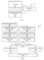
- Figs. 5-6 are flow diagrams showing method for reliability based parameter tuning in accordance with various embodiments of the present invention.
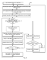
- Fig. 7 is a flow diagram showing another method for reliability based parameter tuning in accordance with some embodiments of the present invention.
- Fig. 8 shows a data processing circuit including known data based tuning circuitry with streamlined search in accordance with one or more embodiments of the present invention.
- the present inventions are related to systems and methods for system characterization, and more particularly to systems and methods for tuning a data processing system.
- Various embodiments of the present invention provide systems and methods for tuning and/or testing a data processing circuit using reliability data generated from any available data set.
- the reliability data may be derived from any available data sets including defined known data sets or unknown user data sets.
- the tuning allows for use of metrics for tuning different channel parameters in such a way that time used to tune the data processing circuit is reduced.
- One or more embodiments of the present invention provide an advantage of reducing storage area required to maintain known data patterns, and/or allow reduced testing and/or tuning times.
- a data processing circuit 100 that includes a reliability monitor circuit 160 that is operable to monitor soft data included as part of a detector output 195 and to modify one or more parameters based upon the monitored soft data.
- Data processing circuit 100 includes an analog processing circuit 108 that includes an analog front end circuit 110, front end processing loops 111 operable to provide timing and control to analog front end circuit 110, and a target circuit 109 operable to provide target based filtering feedback to analog front end circuit 110.
- Analog front end circuit 110 may include, but is not limited to, an analog filter and an amplifier circuit as are known in the art. Based upon the disclosure provided herein, one of ordinary skill in the art will recognize a variety of circuitry that may be included as part of analog front end circuit 110.
- the gain of a variable gain amplifier included as part of analog front circuit 110 may be modifiable, and the cutoff frequency and boost of an analog filter included in analog front end circuit 110 may be modifiable.
- Front end processing loops 111 may be any processing loops operable to provide timing for analog front end circuit 110 known in the art. In some cases, such front end processing loops 111 include a DC loop offset that may be modifiable.
- Target circuit 109 may be any target based filter circuit known in the art. In various cases, a target used by target circuit 109 may be modifiable. Based upon the disclosure provided herein, one of ordinary skill in the art will recognize a variety of target based filter circuits and front end processing loops that may be used in relation to different embodiments of the present invention.
- Analog front end circuit 110 that receives an analog signal 105.
- Analog front end circuit 110 processes analog signal 105 and provides a processed analog signal 112 to an analog to digital converter circuit 114.
- analog signal 105 is derived from a read/write head assembly (not shown) that is disposed in relation to a storage medium (not shown).
- analog signal 105 is derived from a receiver circuit (not shown) that is operable to receive a signal from a transmission medium (not shown).
- the transmission medium may be wired or wireless.
- Analog to digital converter circuit 114 converts processed analog signal 112 into a corresponding series of digital samples 116.
- Analog to digital converter circuit 114 may be any circuit known in the art that is capable of producing digital samples corresponding to an analog input signal. Based upon the disclosure provided herein, one of ordinary skill in the art will recognize a variety of analog to digital converter circuits that may be used in relation to different embodiments of the present invention.
- Digital samples 116 are provided to an equalizer circuit 120.
- Equalizer circuit 120 applies an equalization algorithm to digital samples 116 to yield an equalized output 125.
- equalizer circuit 120 is a digital finite impulse response filter circuit as are known in the art.
- Equalized output 125 is provided to a data detector circuit 130. In some cases, equalizer 120 includes sufficient memory to maintain one or more codewords until a data detector circuit 130 is available for processing.
- Data detector circuit 130 is operable to apply a data detection algorithm to a received codeword or data set, and in some cases data detector circuit 130 can process two or more codewords in parallel.
- data detector circuit 130 is a Viterbi algorithm data detector circuit as are known in the art.
- data detector circuit 130 is a maximum a posteriori data detector circuit as are known in the art.
- the general phrases "Viterbi data detection algorithm” or "Viterbi algorithm data detector circuit” are used in their broadest sense to mean any Viterbi detection algorithm or Viterbi algorithm detector circuit or variations thereof including, but not limited to, bi-direction Viterbi detection algorithm or bi-direction Viterbi algorithm detector circuit.
- maximum a posteriori data detection algorithm or “maximum a posteriori data detector circuit” are used in their broadest sense to mean any maximum a posteriori detection algorithm or detector circuit or variations thereof including, but not limited to, simplified maximum a posteriori data detection algorithm and a max-log maximum a posteriori data detection algorithm, or corresponding detector circuits. Based upon the disclosure provided herein, one of ordinary skill in the art will recognize a variety of data detector circuits that may be used in relation to different embodiments of the present invention. Data detector circuit 130 is started based upon availability of a data set from equalizer circuit 120 or from a central memory circuit 150.
- Detector output 195 includes soft data.
- soft data is used in its broadest sense to mean reliability data with each instance of the reliability data indicating a likelihood that a corresponding bit position or group of bit positions has been correctly detected.
- the soft data or reliability data is log likelihood ratio data as is known in the art.
- Detected output 195 is provided to a local interleaver circuit 142 and reliability monitor circuit 160.
- Local interleaver circuit 142 is operable to shuffle sub-portions (i.e., local chunks) of the data set included as detected output and provides an interleaved codeword 146 that is stored to central memory circuit 150.
- Interleaver circuit 142 may be any circuit known in the art that is capable of shuffling data sets to yield a re-arranged data set. Interleaved codeword 146 is stored to central memory circuit 150.
- a previously stored interleaved codeword 146 is accessed from central memory circuit 150 as a decoder input 152, globally interleaved as is known in the art, and a data decode algorithm is applied.
- the data decode algorithm is a low density parity check algorithm as are known in the art. Based upon the disclosure provided herein, one of ordinary skill in the art will recognize other decode algorithms that may be used in relation to different embodiments of the present invention. As the data decode algorithm completes on a given data set, it is determined whether the decode algorithm converged (i.e., the resulting data set matches the originally written data set as indicated by the lack of parity errors).
- the resulting decoded data set is provided as a hard decision output 172 to a de-interleaver circuit 180.
- De-interleaver circuit 180 rearranges the data to reverse both the global and local interleaving applied to the data to yield a de-interleaved output 182.
- De-interleaved output 182 is provided to a hard decision output circuit 190.
- Hard decision output circuit 190 is operable to re-order data sets that may complete out of order back into their original order. The originally ordered data sets are then provided as a hard decision output 192.
- the completed data set is globally de-interleaved as is known in the art and written back to central memory circuit 150 as a decoder output 154.
- a previously stored decoder output 148 is accessed from central memory circuit 150 and locally de-interleaved by a de-interleaver circuit 144.
- De-interleaver circuit 144 re-arranges decoder output 148 to reverse the shuffling originally performed by interleaver circuit 142.
- a resulting de-interleaved output 197 is provided to data detector circuit 130.
- reliability monitor circuit 160 operates only during a testing/tuning period. In other cases, reliability monitor circuit 160 is continuously operated. Reliability monitor circuit 160 receives detector output 195 and modifies one or more parameter used to govern the operation of data processing circuit 100. The parameters may be communicated to: analog processing circuit 108 via an input/output 164, data detector circuit 130 via an input output 162, and/or to data decoder circuit 170 via an input/output 166.
- the parameters may be, but are not limited to, a gain of a variable gain amplifier included in analog front end circuit 110, a cutoff frequency and/or boost of an analog filter included in analog front end circuit 110, a DC loop offset of front end processing loops 111, a target used by target circuit 109, a detector parameter used by data detector circuit 130, and/or a decoder parameter used by data decoder circuit 170.
- a gain of a variable gain amplifier included in analog front end circuit 110 a cutoff frequency and/or boost of an analog filter included in analog front end circuit 110, a DC loop offset of front end processing loops 111, a target used by target circuit 109, a detector parameter used by data detector circuit 130, and/or a decoder parameter used by data decoder circuit 170.
- Reliability monitor circuit 160 compares the soft data received as part of detector output 195 and compares it against a reliability threshold 168.
- reliability threshold 168 is user programmable. In other cases, reliability threshold 168 is a fixed value.
- reliability monitor circuit 160 selects a value(s) for one or more parameters provided to respective circuits via input/output 162, input/output 164, and input/output 166. Data is then processed through data processing circuit 100 using the selected parameter values over a period of time. Where reliability monitor circuit 160 determines that the soft data from detected output 195 is below reliability threshold 168, an error is indicated. This error is incorporated into an error rate.
- One or more new values for the one or more parameters are selected and the process of retesting continues at least until reliability monitor circuit 160 determines that the corresponding error rate is acceptable.
- a running average or other accumulation of the soft data is used to compare against reliability threshold 168.
- a reset input 169 may be used to reset the accumulation or running average each time a parameter value is changed by reliability monitor circuit 160.
- reset input 169 is a signal internal to reliability monitor circuit 160.
- Reliability based tuning circuit 200 may be used in place of reliability monitor circuit 160 of data processing circuit 100.
- Reliability based tuning circuit 200 includes a comparator circuit 210 that is operable to compare soft data 203 that is received as part of a detected output (not shown) against a reliability threshold 205.
- reliability threshold 205 is user programmable. In other cases, reliability threshold 205 is a fixed value. Where an instance of soft data 203 is less than reliability threshold 205, a comparator output 220 is asserted high.
- comparator output 220 is asserted low.
- a proxy error counter circuit 230 increments.
- the count from proxy error counter circuit 220 is a proxy error count 225 that is provided to a parameter modification control circuit 250.
- Parameter modification control circuit 250 receives an initial parameter value 240 that is initially provided as an updated parameter 260.
- Updated parameter 260 is provided as a parameter to govern operation of one or more functions within a data processing circuit.
- updated parameter 260 may be, but is not limited to, a gain of a variable gain amplifier, a cutoff frequency and/or boost of an analog filter, a DC loop offset, a target, a detector parameter used by a data detector circuit, and/or a decoder parameter used by a data decoder circuit. Based upon the disclosure provided herein, one of ordinary skill in the art will recognize a variety of parameters that may be adjusted by parameter modification control circuit 250.
- parameter modification control circuit 250 allows for a defined number of periods of data processing to continue using initial parameter 240 as updated parameter 260.
- Initial parameter 240 may be a pre-programmed default value.
- proxy error count 225 is stored, and parameter modification circuit 250 selects a new value to be provided as updated parameter 260, and proxy error counter circuit 230 is reset by assertion of a reset signal 223.
- Data processing is again allowed to run for a defined number of periods using the newly selected value of update parameter 260. This process is completed until all possible values for updated parameter 260 have been tested. In the end, the value for updated parameter 260 that yielded the lowest proxy error count 225 is selected as the tuned parameter for whatever circuit updated parameter 260 was controlling. This process is shown in the following pseudo-code:
- parameter modification control circuit 250 may be modified to limit the parameter search by limiting the search until proxy error count 225 falls below a defined threshold. Once a parameter value is found that yields a proxy error count 225 below a defined threshold, that parameter value is selected and the parameter search process is completed.
- the defined threshold may be programmable or fixed in value. This process is shown in the following pseudo-code:
- a more sophisticated testing process may be used such that all values for updated parameter 260 do not need to be tested.
- a streamlined testing process may be done consistent with that discussed below in relation to Figs. 5-6 below.
- the operation of parameter modification control circuit 250 may be modified to use the streamlined approach to identifying an acceptable value for updated parameter 260.
- the methods discussed below in relation to Figs. 5-6 may be modified to search through a variety of parameter values based upon an actual error count derived from a known data set. Such an approach is discussed below in relation to Figs. 8-10.
- Storage system 300 may be, for example, a hard disk drive.
- Storage system 300 also includes a preamplifier 370, an interface controller 320, a hard disk controller 366, a motor controller 368, a spindle motor 372, a disk platter 378, and a read/write head assembly 376.
- Interface controller 320 controls addressing and timing of data to/from disk platter 378.
- the data on disk platter 378 consists of groups of magnetic signals that may be detected by read/write head assembly 376 when the assembly is properly positioned over disk platter 378.
- disk platter 378 includes magnetic signals recorded in accordance with either a longitudinal or a perpendicular recording scheme.
- read/write head assembly 376 is accurately positioned by motor controller 368 over a desired data track on disk platter 378.
- Motor controller 368 both positions read/write head assembly 376 in relation to disk platter 378 and drives spindle motor 372 by moving read/write head assembly to the proper data track on disk platter 378 under the direction of hard disk controller 366.
- Spindle motor 372 spins disk platter 378 at a determined spin rate (RPMs).
- RPMs spin rate
- This minute analog signal is transferred from read/write head assembly 376 to read channel circuit 310 via preamplifier 370.
- Preamplifier 370 is operable to amplify the minute analog signals accessed from disk platter 378.
- read channel circuit 310 decodes and digitizes the received analog signal to recreate the information originally written to disk platter 378.
- This data is provided as read data 303 to a receiving circuit.
- a write operation is substantially the opposite of the preceding read operation with write data 301 being provided to read channel circuit 310. This data is then encoded and written to disk platter 378.
- the reliability data based tuning control circuitry modifies one or more parameters governing the operation of read channel circuit 310 and continues to monitor whether a reliability threshold is met. In this way, parameters in read channel circuit 310 may be modified to improve the performance of read channel circuit 310.
- the processing circuit including the reliability data based tuning control circuitry may be implemented similar to that discussed above in relation to Figs. 1 and 2 , and/or may operate similar to that discussed below in relation to Figs. 5 , 6 , and/or 7. In other cases, the reliability data based tuning control circuitry may be replaced by known data based tuning control circuitry similar to that discussed below in relation to Fig. 8 that uses a streamlined search similar to that discussed below in relation to Figs. 5 and 6 .
- storage system may utilize SATA, SAS or other storage technologies known in the art.
- storage system 300 may be integrated into a larger storage system such as, for example, a RAID (redundant array of inexpensive disks or redundant array of independent disks) based storage system.
- RAID redundant array of inexpensive disks or redundant array of independent disks
- various functions or blocks of storage system 400 may be implemented in either software or firmware, while other functions or blocks are implemented in hardware.
- Data transmission system 400 includes a transmitter 410 that is operable to transmit encoded information via a transfer medium 430 as is known in the art.
- the encoded data is received from transfer medium 430 by receiver 420.
- Receiver 420 incorporates reliability data based tuning circuitry. While processing received data, received data is converted from an analog signal to a series of corresponding digital samples, and the digital samples are equalized to yield an equalized output. The equalized output is then provided to a data processing circuit including both a data detector circuit and a data decoder circuit.
- transfer medium 430 may be any transfer medium known in the art including, but not limited to, a wireless medium, an optical medium, or a wired medium. Based upon the disclosure provided herein, one of ordinary skill in the art will recognize a variety of transfer mediums that may be used in relation to different embodiments of the present invention.
- the reliability data based tuning control circuitry modifies one or more parameters governing the operation of receiver 420 and continues to monitor whether a reliability threshold is met. In this way, parameters in receiver 420 may be modified to improve the performance of receiver 420.
- the processing circuit including the reliability data based tuning control circuitry may be implemented similar to that discussed above in relation to Figs. 1 and 2 , and/or may operate similar to that discussed below in relation to Figs. 5 , 6 , and/or 7. In other cases, the reliability data based tuning control circuitry may be replaced by known data based tuning control circuitry similar to that discussed below in relation to Fig. 8 that uses a streamlined search similar to that discussed below in relation to Figs. 5 and 6 .
- a flow diagram 500 shows a method for reliability based parameter tuning in accordance with various embodiments of the present invention.
- an initial parameter is selected for search (block 505).
- the selected parameter may be any parameter governing operation of some part of a data processing circuit.
- the parameter may be, but is not limited to, a gain of a variable gain amplifier, a cutoff frequency and/or boost of an analog filter, a DC loop offset, a target, a detector parameter used by a data detector circuit, and/or a decoder parameter used by a data decoder circuit. Based upon the disclosure provided herein, one of ordinary skill in the art will recognize a variety of parameters that may be adjusted by the methods of Fig. 5 .
- a current value of the selected parameter is read and stored as a variable PARAM (block 510).
- An updated parameter i.e., a parameter to be applied to the data processing circuit
- Applying the updated parameter to the processing circuit includes operating the processing circuit for a period with the updated parameter. As this processing is done, a count is made of how many instances of soft data from a data detector circuit is less than a defined threshold to yield a proxy error count. Once the processing is done, the proxy error count is read and stored as a variable COUNT (block 520). The proxy error count value is then reset.
- a search direction is calculated (block 600). This process of selecting the search direction is discussed below in more detail in relation to Fig. 6 .
- a value for the updated parameter is calculated based on the search direction and a step size (block 535).
- the step size may be user programmable, while in other cases the step size may be fixed.
- the value of the updated parameter is calculated in accordance with the following pseudo-code:
- NEXT_COUNT It is determined whether the value of NEXT_COUNT is less than or equal to the value of COUNT (block 550). Where the value of NEXT_COUNT is less than or equal to the value of COUNT (block 550), the variable COUNT is set equal to the value of NEXT_COUNT, and the value or PARAM is set equal to the value of the updated parameter (block 555).
- the process of blocks 530, 600, 535, 540, 545, 550, 555 repeats until all values for the selected parameter have been tested.
- a flow diagram 600 shows a method in accordance with some embodiments of the present invention for determining a search direction.
- Flow diagram 600 outlines the method of the block from Fig. 5 of the same number.
- the updated parameter is received from the process of flow diagram 500 (block 602).
- the next value for the updated parameter i.e., a value of the updated parameter increased by a defined amount
- is selected block 605.
- the next value of the updated parameter is applied to the data processing circuit (block 610). Applying the next value of the updated parameter to the processing circuit includes operating the processing circuit for a period with the updated parameter.
- a count is made of how many instances of soft data from a data detector circuit is less than a defined threshold to yield a proxy error count.
- the proxy error count is read and stored as a variable PLUS_COUNT (block 520). The proxy error count value is then reset.
- the prior value of the updated parameter i.e., a value of the updated parameter decreased by the defined amount
- the prior value of the updated parameter is applied to the data processing circuit (block 625). Applying the prior value of the updated parameter to the processing circuit includes operating the processing circuit for a period with the updated parameter. As this processing is done, a count is made of how many instances of soft data from a data detector circuit is less than a defined threshold to yield a proxy error count. Once the processing is done, the proxy error count is read and stored as a variable MINUS_COUNT (block 630). The proxy error count value is then reset.
- a flow diagram 700 shows another method for reliability based parameter tuning in accordance with some embodiments of the present invention.
- an initial parameter is selected for search (block 705).
- the selected parameter may be any parameter governing operation of some part of a data processing circuit.
- the parameter may be, but is not limited to, a gain of a variable gain amplifier, a cutoff frequency and/or boost of an analog filter, a DC loop offset, a target, a detector parameter used by a data detector circuit, and/or a decoder parameter used by a data decoder circuit. Based upon the disclosure provided herein, one of ordinary skill in the art will recognize a variety of parameters that may be adjusted by the methods of Fig. 7 .
- a current value of the selected parameter is read and stored as a variable PARAM (block 710).
- An updated parameter i.e., a parameter to be applied to the data processing circuit
- the updated parameter is applied to the data processing circuit (block 720).
- Applying the updated parameter to the processing circuit includes operating the processing circuit for a period with the updated parameter. As this processing is done, a count is made of how many instances of soft data from a data detector circuit is less than a defined threshold to yield a proxy error count. Once the processing is done, the proxy error count is read and stored as a variable COUNT (block 725). The proxy error count value is then reset.
- NEXT_COUNT It is determined whether the value of NEXT_COUNT is less than or equal to the value of COUNT (block 750). Where the value of NEXT_COUNT is less than or equal to the value of COUNT (block 750), the variable COUNT is set equal to the value of NEXT_COUNT, and the value or PARAM is set equal to the value of the updated parameter (block 755). The process of blocks 730-755 repeats until all values for the selected parameter have been tested.
- the best available value for the selected parameter is stored in the variable PARAM and that value is applied to the data processing circuit (block 760). It is then determined whether another parameter of the data processing circuit remains to be tested (block 765). Where another parameter remains to be tested (block 765), the next parameter to be tested is selected (block 775) and the processes of blocks 710-765 are repeated for the newly selected parameter. Otherwise, where no other parameters remain to be tested (block 765), the testing process is ended (block 770).
- Fig. 8 shows a data processing circuit 800 including known data based monitor circuit 860 with streamlined search in accordance with one or more embodiments of the present invention.
- Data processing circuit 800 includes an analog processing circuit 808 that includes an analog front end circuit 810, front end processing loops 811 operable to provide timing and control to analog front end circuit 810, and a target circuit 809 operable to provide target based filtering feedback to analog front end circuit 810.
- Analog front end circuit 810 may include, but is not limited to, an analog filter and an amplifier circuit as are known in the art. Based upon the disclosure provided herein, one of ordinary skill in the art will recognize a variety of circuitry that may be included as part of analog front end circuit 810.
- the gain of a variable gain amplifier included as part of analog front circuit 810 may be modifiable, and the cutoff frequency and boost of an analog filter included in analog front end circuit 810 may be modifiable.
- Front end processing loops 811 may be any processing loops operable to provide timing for analog front end circuit 810 known in the art. In some cases, such front end processing loops 811 include a DC loop offset that may be modifiable.
- Target circuit 809 may be any target based filter circuit known in the art. In various cases, a target used by target circuit 809 may be modifiable. Based upon the disclosure provided herein, one of ordinary skill in the art will recognize a variety of target based filter circuits and front end processing loops that may be used in relation to different embodiments of the present invention.
- Analog front end circuit 810 that receives an analog signal 805.
- Analog front end circuit 810 processes analog signal 805 and provides a processed analog signal 812 to an analog to digital converter circuit 814.
- analog signal 805 is derived from a read/write head assembly (not shown) that is disposed in relation to a storage medium (not shown).
- analog signal 805 is derived from a receiver circuit (not shown) that is operable to receive a signal from a transmission medium (not shown).
- the transmission medium may be wired or wireless.
- Analog to digital converter circuit 814 converts processed analog signal 812 into a corresponding series of digital samples 816.
- Analog to digital converter circuit 814 may be any circuit known in the art that is capable of producing digital samples corresponding to an analog input signal. Based upon the disclosure provided herein, one of ordinary skill in the art will recognize a variety of analog to digital converter circuits that may be used in relation to different embodiments of the present invention.
- Digital samples 816 are provided to an equalizer circuit 820.
- Equalizer circuit 820 applies an equalization algorithm to digital samples 816 to yield an equalized output 825.
- equalizer circuit 820 is a digital finite impulse response filter circuit as are known in the art.
- Equalized output 825 is provided to a data detector circuit 830. In some cases, equalizer 820 includes sufficient memory to maintain one or more codewords until a data detector circuit 830 is available for processing.
- Data detector circuit 830 is operable to apply a data detection algorithm to a received codeword or data set, and in some cases data detector circuit 830 can process two or more codewords in parallel.
- data detector circuit 830 is a Viterbi algorithm data detector circuit as are known in the art.
- data detector circuit 830 is a maximum a posteriori data detector circuit as are known in the art. Based upon the disclosure provided herein, one of ordinary skill in the art will recognize a variety of data detector circuits that may be used in relation to different embodiments of the present invention.
- Data detector circuit 830 is started based upon availability of a data set from equalizer circuit 820 or from a central memory circuit 850.
- data detector circuit 830 Upon completion, data detector circuit 830 provides detector output 895. Detected output 895 is provided to a local interleaver circuit 842 and known data based monitor circuit 860. Local interleaver circuit 842 is operable to shuffle sub-portions (i.e., local chunks) of the data set included as detected output and provides an interleaved codeword 846 that is stored to central memory circuit 850. Interleaver circuit 842 may be any circuit known in the art that is capable of shuffling data sets to yield a re-arranged data set. Interleaved codeword 846 is stored to central memory circuit 850.
- a previously stored interleaved codeword 846 is accessed from central memory circuit 850 as a decoder input 852, globally interleaved as is known in the art, and a data decode algorithm is applied.
- the data decode algorithm is a low density parity check algorithm as are known in the art. Based upon the disclosure provided herein, one of ordinary skill in the art will recognize other decode algorithms that may be used in relation to different embodiments of the present invention. As the data decode algorithm completes on a given data set, it is determined whether the decode algorithm converged (i.e., the resulting data set matches the originally written data set as indicated by the lack of parity errors).
- the resulting decoded data set is provided as a hard decision output 872 to a de-interleaver circuit 880.
- De-interleaver circuit 880 rearranges the data to reverse both the global and local interleaving applied to the data to yield a de-interleaved output 882.
- De-interleaved output 882 is provided to a hard decision output circuit 890.
- Hard decision output circuit 890 is operable to re-order data sets that may complete out of order back into their original order. The originally ordered data sets are then provided as a hard decision output 892.
- the completed data set is globally de-interleaved as is known in the art and written back to central memory circuit 850 as a decoder output 854.
- a previously stored decoder output 848 is accessed from central memory circuit 850 and locally de-interleaved by a de-interleaver circuit 844.
- De-interleaver circuit 844 re-arranges decoder output 848 to reverse the shuffling originally performed by interleaver circuit 842.
- a resulting de-interleaved output 897 is provided to data detector circuit 830.
- known data based monitor circuit 860 operates only during a testing/tuning period. In other cases, known data based monitor circuit 860 is continuously operated.
- Known data based monitor circuit 860 receives detector output 895 and modifies one or more parameter used to govern the operation of data processing circuit 800. The parameters may be communicated to: analog processing circuit 808 via an input/output 864, data detector circuit 830 via an input output 862, and/or to data decoder circuit 870 via an input/output 866.
- the parameters may be, but are not limited to, a gain of a variable gain amplifier included in analog front end circuit 810, a cutoff frequency and/or boost of an analog filter included in analog front end circuit 810, a DC loop offset of front end processing loops 811, a target used by target circuit 809, a detector parameter used by data detector circuit 830, and/or a decoder parameter used by data decoder circuit 870.
- a gain of a variable gain amplifier included in analog front end circuit 810 a cutoff frequency and/or boost of an analog filter included in analog front end circuit 810, a DC loop offset of front end processing loops 811, a target used by target circuit 809, a detector parameter used by data detector circuit 830, and/or a decoder parameter used by data decoder circuit 870.
- Known data based monitor circuit 860 compares hard decision output 892 against a known data set 868. As data is being processed, known data based monitor circuit 860 selects a value(s) for one or more parameters provided to respective circuits via input/output 862, input/output 864, and input/output 866. Data is then processed through data processing circuit 800 using the selected parameter values over a period of time. Where known data based monitor circuit 860 determines that an instance of hard decision output 892 is not equal to a corresponding instance of known data set 868 an error is indicated. The error is incorporated into an error rate. Where the error rate exceeds a defined threshold, one or more new values for the one or more parameters are selected and the process of retesting continues until an acceptable parameter is identified.
- a circuit similar to that discussed above in relation to Fig. 2 may be used to implement known data based monitor circuit. The difference being that comparator 210 of the circuit of Fig. 2 receives known data set 868 and hard decision output 892 in place of soft data 203 and reliability threshold 205.
- Known data based monitor circuit 860 incorporates a streamlined parameter value search process as discussed above in relation to Figs. 5-6 .
- Such integrated circuits may include all of the functions of a given block, system or circuit, or only a subset of the block, system or circuit. Further, elements of the blocks, systems or circuits may be implemented across multiple integrated circuits. Such integrated circuits may be any type of integrated circuit known in the art including, but are not limited to, a monolithic integrated circuit, a flip chip integrated circuit, a multichip module integrated circuit, and/or a mixed signal integrated circuit. It should also be noted that various functions of the blocks, systems or circuits discussed herein may be implemented in either software or firmware. In some such cases, the entire system, block or circuit may be implemented using its software or firmware equivalent. In other cases, the one part of a given system, block or circuit may be implemented in software or firmware, while other parts are implemented in hardware.
Landscapes
- Engineering & Computer Science (AREA)
- Signal Processing (AREA)
- Computer Networks & Wireless Communication (AREA)
- Power Engineering (AREA)
- Physics & Mathematics (AREA)
- Theoretical Computer Science (AREA)
- Probability & Statistics with Applications (AREA)
- Quality & Reliability (AREA)
- General Physics & Mathematics (AREA)
- General Engineering & Computer Science (AREA)
- Detection And Prevention Of Errors In Transmission (AREA)
- Error Detection And Correction (AREA)
- Signal Processing For Digital Recording And Reproducing (AREA)
- Debugging And Monitoring (AREA)
Abstract
Description
- The present inventions are related to systems and methods for system characterization, and more particularly to systems and methods for tuning a data processing system.
- Various storage systems include data processing circuitry implemented with one or more modifiable variables that may be tuned to improve processing performance. In some cases, known data patterns are provided to the data processing circuitry, and an error rate of the data processing circuitry is monitored while one or more of the modifiable variables are changed. This process is continued until acceptable values for the modifiable variables are identified. Such an approach utilizes storage area for the known pattern thus diminishing the usable storage area, and obtaining a meaningful error rate can take considerable time which increases the costs of manufacturing the storage systems.
- Hence, for at least the aforementioned reasons, there exists a need in the art for advanced systems and methods for data processing.
- The present inventions are related to systems and methods for system characterization, and more particularly to systems and methods for tuning a data processing system. According to a first aspect of the invention, there is provided a data processing system as set out in claim 1. According to another aspect of the invention, there is provided a storage device as set out in claim 13, the storage device comprising: a storage medium; a head assembly disposed in relation to the storage medium and operable to provide a sensed signal corresponding to information on the storage medium; a read channel circuit including: an analog to digital converter circuit operable to sample an analog signal derived from the sensed signal to yield a series of digital samples; an equalizer circuit operable to equalize the digital samples to yield a first data set; a data detector circuit operable to apply a data detection algorithm to the first data set; a data decoder circuit operable to apply a data decode algorithm to a second data set to yield a decoded output, wherein the second data set is derived from the first data set; a reliability monitor circuit operable to calculate an error rate based at least in part on an output selected from a group consisting of: a third data set derived from the decoded output, and the first data set; a parameter modification control circuit operable to: select a first value for a parameter and to store a first instance of the error rate corresponding to the first value; select a second value for the parameter and to store a second instance of error count corresponding to the second value, wherein selecting the second value includes: determining a search direction based at least in part on the first value; and using the search value and a step size to calculate the second value; and select one of the first value and the second value based at least in part on a comparison of the first instance of the error rate and the second instance of the error rate.
- One or more embodiments of the present invention provide data processing systems that include: a data detector circuit; a data decoder circuit, a reliability monitor circuit, and a parameter modification control circuit. The data detector circuit is operable to apply a data detection algorithm to a first data set guided by a decoded output to yield a detected output. The data decoder circuit is operable to apply a data decode algorithm to a second data set to yield the decoded output. The second data set is derived from the first data set. The reliability monitor circuit is operable to calculate an error rate. The error rate may be calculated based at least in part on a third data set derived from the decoded output or the first data set. The parameter modification circuit is operable to: select a first value for a parameter and to store a first instance of the error rate corresponding to the first value; select a second value for the parameter and to store a second instance of error count corresponding to the second value, and select one of the first value and the second value based at least in part on a comparison of the first instance of the error rate and the second instance of the error rate. Selecting the second value includes: determining a search direction based at least in part on the first value; and using the search value and a step size to calculate the second value. In some cases, the steps size is programmable. The embodiments may be implemented in a number of different end devices or systems. For example, the embodiments may be implemented in a storage device or a receiving device. Further, in some cases, the data processing systems may be implemented as part of an integrated circuit.
- In some instances of the aforementioned embodiments, calculating the error rate includes comparing the third data set against a known data set. In some such instances, the third data set is a set of hard decision outputs. The data detection algorithm may be, but is not limited to, a maximum a posteriori data detection algorithm or a Viterbi detection algorithm. In some cases, the data decode algorithm is a low density parity check algorithm. In particular cases, the output is the third data set derived from the decoded output. In such cases, the reliability monitor circuit may include: a comparator circuit operable to compare instances of the third data set against a known data set; and a counter circuit operable to increment when an instance of the third data set is not equal to a corresponding instance of the known data set to yield the error rate. In some cases, the output is the first data set that includes soft data. In such cases, the reliability monitor circuit may include: a comparator circuit operable to compare instances of the soft data against a threshold value; and a counter circuit operable to increment when an instance of the soft data is less than the threshold value to yield the error rate. In particular cases, the threshold value is programmable.
- According to another aspect of the invention, there is provided a method for data processing as set out in claim 9. Some embodiments of the present invention provide methods for data processing. The methods include: performing a data detection algorithm using a data detector circuit on a first data set to yield a detected output; performing a data decode algorithm using a data decoder circuit on a second data set derived from the first data set to yield a decoded output; calculating an error rate based at least in part on one of a third data set derived from the decoded output, or the first data set; selecting a first value for a parameter and storing a first instance of the error rate corresponding to the first value; selecting a second value for the parameter and storing a second instance of error count corresponding to the second value, and selecting one of the first value and the second value based at least in part on a comparison of the first instance of the error rate and the second instance of the error rate. Selecting the second value includes: determining a search direction based at least in part on the first value; and using the search value and a step size to calculate the second value. In some cases, the third data set is a set of hard decision outputs. In various cases, the steps size is programmable.
- In some case, the output is the third data set derived from the decoded output. In some such cases, calculating the error rate includes: comparing instances of the third data set against a known data set; and counting the number of instances of the third data set that are not equal to a corresponding instance of the known data set to yield the error rate. In other cases, the output is the first data set that includes soft data. In some such cases, calculating the error rate includes: comparing instances of the soft data against a threshold value; and counting the number of instances of the soft data that are less than the threshold value to yield the error rate. In particular cases, the threshold value is programmable.
- Various embodiments of the present invention provide data processing systems that include: a data detector circuit, and a reliability monitor circuit. The data detector circuit is operable to apply a data detection algorithm to a data set to yield a detected output that includes soft data. The reliability monitor circuit is operable to determine a proxy error count based at least in part on the soft data, and to modify a parameter governing an operation of the data processing system based at least in part on the proxy error count. In some cases, the aforementioned embodiments of the present invention are implemented as part of a storage device or a receiving device. In some cases, the aforementioned embodiments of the present invention are implemented as part of an integrated circuit.
- In some instances of the aforementioned embodiments, the data detection algorithm is a maximum a posteriori data detection algorithm. In other instances, the data detection algorithm is a Viterbi detection algorithm. In some cases, the data processing system further includes a data decoder circuit operable to apply a data decode algorithm to a derivative of the detected output to yield a decoded output. In some cases, the data decode algorithm is a low density parity check algorithm.
- In some cases, the reliability monitor circuit includes: a comparator circuit that is operable to compare instances of the soft data against a threshold value; and a counter circuit that is operable to increment when an instance of the soft data is less than the threshold value to yield the proxy error count. In some such cases, the threshold value is programmable. In various of such cases, the reliability monitor circuit further includes a parameter modification control circuit that is operable to: select a first value for the parameter and to store a first instance of the proxy error count corresponding to the first value; select a second value for the parameter and to store a second instance of the proxy error count corresponding to the first value; and select one of the first value and the second value based at least in part on a comparison of the first instance of the proxy error count and the second instance of the proxy error count. In some particular cases, selecting the second value for the parameter includes: determining a search direction based at least in part on the first value; and using the search value and a step size to calculate the second value. In some cases, the steps size is programmable. In other cases, selecting the first value for the parameter includes selecting one of a number of values to be searched; and selecting the second value for the parameter includes selecting another of the number of values to be searched.
- Other embodiments of the present invention provide methods for data processing that include: performing a data detection algorithm using a data detector circuit on a data set to yield a detected output that includes soft data; comparing instances of the soft data against a threshold value; modifying a proxy error count value based at least in part on the comparison of the instances of the soft data against the threshold value; and selecting a parameter value based at least in part on the proxy error count, wherein the parameter value governs an operation of a data processing circuit. In some instances of the aforementioned embodiments, the data set includes a pattern of data that may be a known data pattern, or an unknown data pattern.
- In some instances of the aforementioned embodiments, the detected output is a first detected output, the soft data is a first soft data, the parameter value is a first parameter value, wherein the proxy error count is a first proxy error count, the data set is a first data set. In such instances, the methods may further include: performing a data detection algorithm on a second data set to yield a second detected output that includes a second soft data; comparing instances of the second soft data against the threshold value; modifying a second proxy error count value based at least in part on the comparison of the instances of the second soft data against the threshold value; and comparing the first proxy error count with the second proxy error count. In such instances, selecting the first parameter value is based on the comparison of the first proxy error count with the second proxy error count. In some cases, the first parameter value is applied to the data processing circuit while the data detector circuit applies the data detection algorithm to the first data set, and the second parameter value is applied to the data processing circuit while the data detector circuit applies the data detection algorithm to the second data set.
- This summary provides only a general outline of some embodiments of the invention. Many other objects, features, advantages and other embodiments of the invention will become more fully apparent from the following detailed description, the appended claims and the accompanying drawings.
- A further understanding of the various embodiments of the present invention may be realized by reference to the figures which are described in remaining portions of the specification. In the figures, like reference numerals are used throughout several figures to refer to similar components. In some instances, a sub-label consisting of a lower case letter is associated with a reference numeral to denote one of multiple similar components. When reference is made to a reference numeral without specification to an existing sub-label, it is intended to refer to all such multiple similar components.
-
Fig. 1 shows a data processing circuit including reliability data based tuning circuitry in accordance with one or more embodiments of the present invention; -
Fig. 2 depicts one implementation of a reliability based tuning circuit in accordance with some embodiments of the present invention; -
Fig. 3 shows a storage device including a read channel having soft data based tuning circuitry in accordance with one or more embodiments of the present invention; -
Fig. 4 shows a data transmission system including a receiver having soft data based tuning circuitry in accordance with some embodiments of the present invention; -
Figs. 5-6 are flow diagrams showing method for reliability based parameter tuning in accordance with various embodiments of the present invention; -
Fig. 7 is a flow diagram showing another method for reliability based parameter tuning in accordance with some embodiments of the present invention; and -
Fig. 8 shows a data processing circuit including known data based tuning circuitry with streamlined search in accordance with one or more embodiments of the present invention. - The present inventions are related to systems and methods for system characterization, and more particularly to systems and methods for tuning a data processing system.
- Various embodiments of the present invention provide systems and methods for tuning and/or testing a data processing circuit using reliability data generated from any available data set. The reliability data may be derived from any available data sets including defined known data sets or unknown user data sets. In some cases, the tuning allows for use of metrics for tuning different channel parameters in such a way that time used to tune the data processing circuit is reduced. One or more embodiments of the present invention provide an advantage of reducing storage area required to maintain known data patterns, and/or allow reduced testing and/or tuning times.
- Turning to
Fig. 1 , adata processing circuit 100 is shown that includes areliability monitor circuit 160 that is operable to monitor soft data included as part of adetector output 195 and to modify one or more parameters based upon the monitored soft data.Data processing circuit 100 includes ananalog processing circuit 108 that includes an analogfront end circuit 110, front end processing loops 111 operable to provide timing and control to analogfront end circuit 110, and atarget circuit 109 operable to provide target based filtering feedback to analogfront end circuit 110. Analogfront end circuit 110 may include, but is not limited to, an analog filter and an amplifier circuit as are known in the art. Based upon the disclosure provided herein, one of ordinary skill in the art will recognize a variety of circuitry that may be included as part of analogfront end circuit 110. In some cases, the gain of a variable gain amplifier included as part of analogfront circuit 110 may be modifiable, and the cutoff frequency and boost of an analog filter included in analogfront end circuit 110 may be modifiable. Front end processing loops 111 may be any processing loops operable to provide timing for analogfront end circuit 110 known in the art. In some cases, such front end processing loops 111 include a DC loop offset that may be modifiable.Target circuit 109 may be any target based filter circuit known in the art. In various cases, a target used bytarget circuit 109 may be modifiable. Based upon the disclosure provided herein, one of ordinary skill in the art will recognize a variety of target based filter circuits and front end processing loops that may be used in relation to different embodiments of the present invention. - Analog
front end circuit 110 that receives ananalog signal 105. Analogfront end circuit 110processes analog signal 105 and provides a processedanalog signal 112 to an analog todigital converter circuit 114. In some cases,analog signal 105 is derived from a read/write head assembly (not shown) that is disposed in relation to a storage medium (not shown). In other cases,analog signal 105 is derived from a receiver circuit (not shown) that is operable to receive a signal from a transmission medium (not shown). The transmission medium may be wired or wireless. Based upon the disclosure provided herein, one of ordinary skill in the art will recognize a variety of sources from whichanalog input 105 may be derived. - Analog to
digital converter circuit 114 converts processedanalog signal 112 into a corresponding series ofdigital samples 116. Analog todigital converter circuit 114 may be any circuit known in the art that is capable of producing digital samples corresponding to an analog input signal. Based upon the disclosure provided herein, one of ordinary skill in the art will recognize a variety of analog to digital converter circuits that may be used in relation to different embodiments of the present invention.Digital samples 116 are provided to anequalizer circuit 120.Equalizer circuit 120 applies an equalization algorithm todigital samples 116 to yield an equalizedoutput 125. In some embodiments of the present invention,equalizer circuit 120 is a digital finite impulse response filter circuit as are known in the art. Equalizedoutput 125 is provided to adata detector circuit 130. In some cases,equalizer 120 includes sufficient memory to maintain one or more codewords until adata detector circuit 130 is available for processing. -
Data detector circuit 130 is operable to apply a data detection algorithm to a received codeword or data set, and in some casesdata detector circuit 130 can process two or more codewords in parallel. In some embodiments of the present invention,data detector circuit 130 is a Viterbi algorithm data detector circuit as are known in the art. In other embodiments of the present invention,data detector circuit 130 is a maximum a posteriori data detector circuit as are known in the art. Of note, the general phrases "Viterbi data detection algorithm" or "Viterbi algorithm data detector circuit" are used in their broadest sense to mean any Viterbi detection algorithm or Viterbi algorithm detector circuit or variations thereof including, but not limited to, bi-direction Viterbi detection algorithm or bi-direction Viterbi algorithm detector circuit. Also, the general phrases "maximum a posteriori data detection algorithm" or "maximum a posteriori data detector circuit" are used in their broadest sense to mean any maximum a posteriori detection algorithm or detector circuit or variations thereof including, but not limited to, simplified maximum a posteriori data detection algorithm and a max-log maximum a posteriori data detection algorithm, or corresponding detector circuits. Based upon the disclosure provided herein, one of ordinary skill in the art will recognize a variety of data detector circuits that may be used in relation to different embodiments of the present invention.Data detector circuit 130 is started based upon availability of a data set fromequalizer circuit 120 or from acentral memory circuit 150. - Upon completion,
data detector circuit 130 providesdetector output 195.Detector output 195 includes soft data. As used herein, the phrase "soft data" is used in its broadest sense to mean reliability data with each instance of the reliability data indicating a likelihood that a corresponding bit position or group of bit positions has been correctly detected. In some embodiments of the present invention, the soft data or reliability data is log likelihood ratio data as is known in the art. Detectedoutput 195 is provided to alocal interleaver circuit 142 andreliability monitor circuit 160.Local interleaver circuit 142 is operable to shuffle sub-portions (i.e., local chunks) of the data set included as detected output and provides an interleavedcodeword 146 that is stored tocentral memory circuit 150.Interleaver circuit 142 may be any circuit known in the art that is capable of shuffling data sets to yield a re-arranged data set. Interleavedcodeword 146 is stored tocentral memory circuit 150. - Once
data decoder circuit 170 is available, a previously stored interleavedcodeword 146 is accessed fromcentral memory circuit 150 as adecoder input 152, globally interleaved as is known in the art, and a data decode algorithm is applied. In some embodiments of the present invention, the data decode algorithm is a low density parity check algorithm as are known in the art. Based upon the disclosure provided herein, one of ordinary skill in the art will recognize other decode algorithms that may be used in relation to different embodiments of the present invention. As the data decode algorithm completes on a given data set, it is determined whether the decode algorithm converged (i.e., the resulting data set matches the originally written data set as indicated by the lack of parity errors). Where it is determined that the decode algorithm converged, the resulting decoded data set is provided as ahard decision output 172 to ade-interleaver circuit 180.De-interleaver circuit 180 rearranges the data to reverse both the global and local interleaving applied to the data to yield ade-interleaved output 182.De-interleaved output 182 is provided to a harddecision output circuit 190. Harddecision output circuit 190 is operable to re-order data sets that may complete out of order back into their original order. The originally ordered data sets are then provided as ahard decision output 192. - Alternatively, where it is determined that the data decode algorithm failed to converge (i.e., there are remaining parity errors), the completed data set is globally de-interleaved as is known in the art and written back to
central memory circuit 150 as adecoder output 154. Oncedata detector circuit 130 is available, a previously storeddecoder output 148 is accessed fromcentral memory circuit 150 and locally de-interleaved by a de-interleaver circuit 144. De-interleaver circuit 144re-arranges decoder output 148 to reverse the shuffling originally performed byinterleaver circuit 142. A resultingde-interleaved output 197 is provided todata detector circuit 130. - In some cases,
reliability monitor circuit 160 operates only during a testing/tuning period. In other cases,reliability monitor circuit 160 is continuously operated.Reliability monitor circuit 160 receivesdetector output 195 and modifies one or more parameter used to govern the operation ofdata processing circuit 100. The parameters may be communicated to:analog processing circuit 108 via an input/output 164,data detector circuit 130 via aninput output 162, and/or todata decoder circuit 170 via an input/output 166. The parameters may be, but are not limited to, a gain of a variable gain amplifier included in analogfront end circuit 110, a cutoff frequency and/or boost of an analog filter included in analogfront end circuit 110, a DC loop offset of front end processing loops 111, a target used bytarget circuit 109, a detector parameter used bydata detector circuit 130, and/or a decoder parameter used bydata decoder circuit 170. Based upon the disclosure provided herein, one of ordinary skill in the art will recognize a variety of parameters that may be adjusted byreliability monitor circuit 160 in accordance with different embodiments of the present invention. -
Reliability monitor circuit 160 compares the soft data received as part ofdetector output 195 and compares it against a reliability threshold 168. In some cases, reliability threshold 168 is user programmable. In other cases, reliability threshold 168 is a fixed value. As data is being processed,reliability monitor circuit 160 selects a value(s) for one or more parameters provided to respective circuits via input/output 162, input/output 164, and input/output 166. Data is then processed throughdata processing circuit 100 using the selected parameter values over a period of time. Wherereliability monitor circuit 160 determines that the soft data from detectedoutput 195 is below reliability threshold 168, an error is indicated. This error is incorporated into an error rate. One or more new values for the one or more parameters are selected and the process of retesting continues at least untilreliability monitor circuit 160 determines that the corresponding error rate is acceptable. In some cases, a running average or other accumulation of the soft data is used to compare against reliability threshold 168. In such cases, areset input 169 may be used to reset the accumulation or running average each time a parameter value is changed byreliability monitor circuit 160. In various cases, resetinput 169 is a signal internal toreliability monitor circuit 160. - Turning to
Fig. 2 , one implementation of a reliability basedtuning circuit 200 is shown in accordance with some embodiments of the present invention. Reliability basedtuning circuit 200 may be used in place ofreliability monitor circuit 160 ofdata processing circuit 100. Reliability basedtuning circuit 200 includes acomparator circuit 210 that is operable to comparesoft data 203 that is received as part of a detected output (not shown) against areliability threshold 205. In some cases,reliability threshold 205 is user programmable. In other cases,reliability threshold 205 is a fixed value. Where an instance ofsoft data 203 is less thanreliability threshold 205, acomparator output 220 is asserted high. In contrast, where an instance ofsoft data 203 is greater than or equal toreliability threshold 205,comparator output 220 is asserted low. On each clock period (corresponding to the instances of soft data 203) thatcomparator output 220 is asserted high, a proxyerror counter circuit 230 increments. The count from proxyerror counter circuit 220 is aproxy error count 225 that is provided to a parametermodification control circuit 250. - Parameter
modification control circuit 250 receives aninitial parameter value 240 that is initially provided as an updatedparameter 260. Updatedparameter 260 is provided as a parameter to govern operation of one or more functions within a data processing circuit. As some examples, updatedparameter 260 may be, but is not limited to, a gain of a variable gain amplifier, a cutoff frequency and/or boost of an analog filter, a DC loop offset, a target, a detector parameter used by a data detector circuit, and/or a decoder parameter used by a data decoder circuit. Based upon the disclosure provided herein, one of ordinary skill in the art will recognize a variety of parameters that may be adjusted by parametermodification control circuit 250. - In one particular embodiment of the present invention , parameter
modification control circuit 250 allows for a defined number of periods of data processing to continue usinginitial parameter 240 as updatedparameter 260.Initial parameter 240 may be a pre-programmed default value. Once the period has completed,proxy error count 225 is stored, andparameter modification circuit 250 selects a new value to be provided as updatedparameter 260, and proxyerror counter circuit 230 is reset by assertion of areset signal 223. Data processing is again allowed to run for a defined number of periods using the newly selected value ofupdate parameter 260. This process is completed until all possible values for updatedparameter 260 have been tested. In the end, the value for updatedparameter 260 that yielded the lowestproxy error count 225 is selected as the tuned parameter for whatever circuit updatedparameter 260 was controlling. This process is shown in the following pseudo-code:
/* Test Initial Parameter Value
        Select Initial Parameter 240 as Updated Parameter 260;
        Assert Reset 225;
        De-assert Reset 225;
        For (i = 0 to end of the Test Period)
        {
             If (Soft Data [i] 203 < Reliability Threshold 205)
             {
                Proxy Error Count 225 += 1
              }
        }
        Parameter Error Count = Proxy Error Count 225;
        Parameter Value = Initial Parameter 240;
        /* Test All Other Parameter Values */
        Assert Reset 225;
        De-assert Reset 225;
        For (Each Value of Updated Parameter 260)
        {
             Select Next Value for Updated Parameter 260;
             For (i = 0 to end of the Test Period)
             {
                 If (Soft Data [i] 203 < Reliability Threshold 205)
                 {
                    Proxy Error Count 225 += 1
                 }
              }
             If (Proxy Error Count 225 < Parameter Error Count)
              {
                 Parameter Error Count = Proxy Error Count 225;
                 Parameter Value = Selected Next Value;
              }
            }
        }
        Select the Parameter Value.
        /* Test Initial Parameter Value
        Select Initial Parameter 240 as Updated Parameter 260;
        Assert Reset 225;
        De-assert Reset 225;
        For (i = 0 to end of the Test Period)
        {
             If (Soft Data [i] 203 < Reliability Threshold 205)
             {
                Proxy Error Count 225 += 1
              }
        }
        If (Proxy Error Count < Defined Threshold)
        {
             Updated Parameter 260 = Initial Parameter 240;
             End Process
        Else
        {
             Parameter Error Count = Proxy Error Count 225;
             Parameter Value = Initial Parameter 240;
        }
        /* Test Other Parameter Values Until Defined Threshold is Achieved*/
        Assert Reset 225;
        De-assert Reset 225;
        For (Each Value of Updated Parameter 260)
        {
             Select Next Value for Updated Parameter 260;
             For (i = 0 to end of the Test Period)
             {
                 If (Soft Data [i] 203 < Reliability Threshold 205)
                 {
                    Proxy Error Count 225 += 1
                 }
              }
             If (Proxy Error Count < Defined Threshold)
              {
                  Updated Parameter 260 = Selected Next Value;
                  End Process
              }
             Else If (Proxy Error Count 225 < Parameter Error Count)
              {
                 Parameter Error Count = Proxy Error Count 225;
                 Parameter Value = Selected Next Value;
              }
            }
        }
        If (Search Direction is Positive)
        {
               Updated Parameter = Updated Parameter + Step Size
        }
        Else
        {
               Updated Parameter = Updated Parameter - Step Size
        }
This newly updated parameter is then applied to the data processing circuit (block 540). Applying the updated parameter to the processing circuit includes operating the processing circuit for a period with the updated parameter. As this processing is done, a count is made of how many instances of soft data from a data detector circuit is less than a defined threshold to yield a proxy error count. Once the processing is done, the proxy error count is read and stored as a variable NEXT_COUNT (block 545). The proxy error count value is then reset.
Claims (15)
- A data processing system, the data processing system comprising:a data detector circuit (130) operable to apply a data detection algorithm to a first data set (125) guided by a decoded output to yield a detected output (195);a data decoder circuit (170) operable to apply a data decode algorithm to a second data set to yield the decoded output, wherein the second data set is derived from the first data set;a reliability monitor circuit (160) operable to calculate an error rate (225) based at least in part on an output selected from a group consisting of: a third data set derived from the decoded output, and the first data set;a parameter modification control circuit (250) operable to:select a first value for a parameter (240) and to store a first instance of the error rate (225) corresponding to the first value;select a second value for the parameter (240) and to store a second instance of error count (225) corresponding to the second value, wherein selecting the second value includes: determining a search direction based at least in part on the first value; and using the search value and a step size to calculate the second value; andselect one of the first value and the second value based at least in part on a comparison of the first instance of the error rate and the second instance of the error rate.
- The data processing system of claim 1, wherein calculating the error rate includes comparing the third data set against a known data set, and/or wherein the third data set is a set of hard decision outputs, and/or wherein the data decode algorithm is a low density parity check algorithm.
- The data processing system of claim 1 or claim 2, wherein the data detection algorithm is selected from a group consisting of: a maximum a posteriori data detection algorithm and a Viterbi detection algorithm.
- The data processing system of any one of the preceding claims, wherein the output is the third data set derived from the decoded output, and wherein the reliability monitor circuit (160) comprises:a comparator circuit (210) operable to compare instances of the third data set against a known data set; anda counter circuit (230) operable to increment when an instance of the third data set is not equal to a corresponding instance of the known data set to yield the error rate.
- The data processing circuit of any one of the preceding claims, wherein the output is the first data set, wherein the first data set includes soft data, and wherein the reliability monitor circuit (160) comprises:a comparator circuit (210) operable to compare instances of the soft data against a threshold value; anda counter circuit (230) operable to increment when an instance of the soft data is less than the threshold value to yield the error rate; andwherein the threshold value may be programmable.
- The data processing system of any one of the preceding claims, wherein the steps size is programmable.
- The data processing circuit of any one of the preceding claims, wherein the data processing system is implemented as part of a device selected from a group consisting of: a storage device (300) and a receiving device (420).
- The data processing system of any one of the preceding claims, wherein the data processing system is implemented as part of an integrated circuit.
- A method for data processing, the method comprising:performing a data detection algorithm using a data detector circuit (130) on a first data set (125) to yield a detected output (195);performing a data decode algorithm using a data decoder circuit (170) on a second data set (152) derived from the first data set (125) to yield a decoded output (172);calculating an error rate (225) based at least in part on an output selected from a group consisting of: a third data set derived from the decoded output, and the first data set;selecting a first value for a parameter (240) and storing a first instance of the error rate (225) corresponding to the first value;selecting a second value for the parameter (240) and storing a second instance of error count (225) corresponding to the second value, wherein selecting the second value includes: determining a search direction based at least in part on the first value; and using the search value and a step size to calculate the second value; andselecting one of the first value and the second value based at least in part on a comparison of the first instance of the error rate and the second instance of the error rate.
- The method of claim 9, wherein the output is the third data set derived from the decoded output, and wherein calculating the error rate comprises:comparing instances of the third data set against a known data set; andcounting the number of instances of the third data set that are not equal to a corresponding instance of the known data set to yield the error rate.
- The method of claim 9 or claim 10, wherein the output is the first data set, wherein the first data set includes soft data, and wherein calculating the error rate comprises:comparing instances of the soft data against a threshold value; andcounting the number of instances of the soft data that are less than the threshold value to yield the error rate; andwherein the threshold value may be programmable.
- The method of any one of claims 9 to 11, wherein the third data set is a set of hard decision outputs (172); and/or wherein the steps size is programmable.
- A storage device (300), the storage device comprising:a storage medium (378);a head assembly (376) disposed in relation to the storage medium (378) and operable to provide a sensed signal corresponding to information on the storage medium (378);a read channel circuit (310) including:an analog to digital converter circuit (114) operable to sample an analog signal (105) derived from the sensed signal to yield a series of digital samples (116);an equalizer circuit (120) operable to equalize the digital samples (116) to yield a first data set (125);a data detector circuit (130) operable to apply a data detection algorithm to the first data set (125);a data decoder circuit (170) operable to apply a data decode algorithm to a second data set (152) to yield a decoded output (172), wherein the second data set (152) is derived from the first data set (125);a reliability monitor circuit (160) operable to calculate an error rate based at least in part on an output selected from a group consisting of: a third data set derived from the decoded output, and the first data set;a parameter modification control circuit (250) operable to:select a first value for a parameter (240) and to store a first instance of the error rate (225) corresponding to the first value;select a second value for the parameter (240) and to store a second instance of error count (225) corresponding to the second value, wherein selecting the second value includes: determining a search direction based at least in part on the first value; and using the search value and a step size to calculate the second value; andselect one of the first value and the second value based at least in part on a comparison of the first instance of the error rate and the second instance of the error rate.
- The storage device of claim 13, wherein the output is the third data set derived from the decoded output, and wherein the reliability monitor circuit (160) comprises:a comparator circuit (210) operable to compare instances of the third data set against a known data set; anda counter circuit (230) operable to increment when an instance of the third data set is not equal to a corresponding instance of the known data set to yield the error rate.
- The storage device of claim 13 or claim 14, wherein the output is the first data set, wherein the first data set includes soft data, and wherein the reliability monitor circuit (160) comprises:a comparator circuit (210) operable to compare instances of the soft data against a threshold value; anda counter circuit (230) operable to increment when an instance of the soft data is less than the threshold value to yield the error rate.
Applications Claiming Priority (1)
| Application Number | Priority Date | Filing Date | Title |
|---|---|---|---|
| US13/251,340 US8479086B2 (en) | 2011-10-03 | 2011-10-03 | Systems and methods for efficient parameter modification |
Publications (2)
| Publication Number | Publication Date |
|---|---|
| EP2613321A2 true EP2613321A2 (en) | 2013-07-10 |
| EP2613321A3 EP2613321A3 (en) | 2015-12-16 |
Family
ID=47010221
Family Applications (1)
| Application Number | Title | Priority Date | Filing Date |
|---|---|---|---|
| EP12183906.2A Withdrawn EP2613321A3 (en) | 2011-10-03 | 2012-09-11 | Systems and methods for efficient parameter modification |
Country Status (6)
| Country | Link |
|---|---|
| US (1) | US8479086B2 (en) |
| EP (1) | EP2613321A3 (en) |
| JP (1) | JP5551739B2 (en) |
| KR (1) | KR101390566B1 (en) |
| CN (1) | CN103034555A (en) |
| TW (1) | TWI443648B (en) |
Cited By (1)
| Publication number | Priority date | Publication date | Assignee | Title |
|---|---|---|---|---|
| US9569641B2 (en) | 2015-03-24 | 2017-02-14 | Nxp Usa, Inc. | Data processing system with temperature monitoring for security |
Families Citing this family (13)
| Publication number | Priority date | Publication date | Assignee | Title |
|---|---|---|---|---|
| US8819519B2 (en) * | 2012-06-28 | 2014-08-26 | Lsi Corporation | Systems and methods for enhanced accuracy NPML calibration |
| US8908304B2 (en) | 2012-07-17 | 2014-12-09 | Lsi Corporation | Systems and methods for channel target based CBD estimation |
| US9324363B2 (en) | 2013-06-05 | 2016-04-26 | Avago Technologies General Ip (Singapore) Pte. Ltd. | Systems and methods for floating variance branch metric calculation |
| US9019642B1 (en) * | 2014-04-02 | 2015-04-28 | Lsi Corporation | Synchronization mark detection for multi-dimensional magnetic recording |
| US10014026B1 (en) | 2017-06-20 | 2018-07-03 | Seagate Technology Llc | Head delay calibration and tracking in MSMR systems |
| US10297281B1 (en) | 2017-11-06 | 2019-05-21 | Seagate Technology Llc | Servo sector detection |
| US10522177B1 (en) | 2018-07-31 | 2019-12-31 | Seagate Technology Llc | Disc locked clock-based servo timing |
| US11016681B1 (en) | 2018-07-31 | 2021-05-25 | Seagate Technology Llc | Multi-threshold parameter adaptation |
| US11018842B1 (en) | 2018-07-31 | 2021-05-25 | Seagate Technology Llc | Dynamic timing recovery bandwidth modulation for phase offset mitigation |
| US10803902B1 (en) | 2018-08-19 | 2020-10-13 | Seagate Technology Llc | Hardware-based read sample averaging |
| US10460762B1 (en) | 2018-09-04 | 2019-10-29 | Seagate Technology Llc | Cancelling adjacent track interference signal with different data rate |
| US10468060B1 (en) | 2018-09-27 | 2019-11-05 | Seagate Technology Llc | Cancelling adjacent track interference |
| US11580042B2 (en) | 2020-11-30 | 2023-02-14 | Seagate Technology Llc | Automated and intelligent data channel optimizers with sensitivity assessment |
Family Cites Families (143)
| Publication number | Priority date | Publication date | Assignee | Title |
|---|---|---|---|---|
| JPH0443721A (en) | 1990-06-11 | 1992-02-13 | Matsushita Electric Ind Co Ltd | Digital signal decoder |
| US5612964A (en) | 1991-04-08 | 1997-03-18 | Haraszti; Tegze P. | High performance, fault tolerant orthogonal shuffle memory and method |
| US5325402A (en) | 1991-04-30 | 1994-06-28 | Nec Corporation | Method and arrangement for estimating data sequences transmsitted using Viterbi algorithm |
| US5278703A (en) | 1991-06-21 | 1994-01-11 | Digital Equipment Corp. | Embedded servo banded format for magnetic disks for use with a data processing system |
| US5311087A (en) | 1991-07-12 | 1994-05-10 | Pioneer Electronic Corporation | Noise removing circuit |
| US5392299A (en) | 1992-01-15 | 1995-02-21 | E-Systems, Inc. | Triple orthogonally interleaed error correction system |
| US5317472A (en) | 1992-03-17 | 1994-05-31 | Schweitzer Engineering Laboratories, Inc. | Apparatus for insuring the security of output signals from protective relays used in electric power systems |
| US5513192A (en) | 1992-08-28 | 1996-04-30 | Sun Microsystems, Inc. | Fault tolerant disk drive system with error detection and correction |
| EP0631277A3 (en) | 1993-06-22 | 1995-02-22 | Quantum Corp | ID-less data sector format and data controller for disk drive. |
| ZA947317B (en) | 1993-09-24 | 1995-05-10 | Qualcomm Inc | Multirate serial viterbi decoder for code division multiple access system applications |
| US5523903A (en) | 1993-12-23 | 1996-06-04 | International Business Machines Corporation | Sector architecture for fixed block disk drive |
| US5550870A (en) | 1994-03-02 | 1996-08-27 | Lucent Technologies Inc. | Viterbi processor |
| JPH07245635A (en) | 1994-03-04 | 1995-09-19 | Sony Corp | Signal point mapping method and signal point detection method |
| US5471500A (en) | 1994-03-08 | 1995-11-28 | At&T Ipm Corp. | Soft symbol decoding |
| EP0677967A3 (en) | 1994-04-12 | 1997-07-23 | Gold Star Co | Viterbi decoder for a high definition television. |
| JP3328093B2 (en) | 1994-07-12 | 2002-09-24 | 三菱電機株式会社 | Error correction device |
| US5734598A (en) * | 1994-12-28 | 1998-03-31 | Quantum Corporation | Low power filter coefficient adaptation circuit for digital adaptive filter |
| US5898710A (en) | 1995-06-06 | 1999-04-27 | Globespan Technologies, Inc. | Implied interleaving, a family of systematic interleavers and deinterleavers |
| US5701314A (en) | 1995-12-21 | 1997-12-23 | Cirrus Logic, Inc. | On-the-fly error correction using thermal asperity erasure pointers from a sampled amplitude read channel in a magnetic disk drive |
| JPH09232973A (en) | 1996-02-28 | 1997-09-05 | Sony Corp | Viterbi decoder |
| US6023783A (en) | 1996-05-15 | 2000-02-08 | California Institute Of Technology | Hybrid concatenated codes and iterative decoding |
| US5978414A (en) | 1996-07-03 | 1999-11-02 | Matsushita Electric Industrial Co., Ltd. | Transmission rate judging unit |
| SG52990A1 (en) | 1996-07-09 | 1998-09-28 | Ibm | Improvements to radial self-propagation pattern generation for disk file servowriting |
| US5802118A (en) | 1996-07-29 | 1998-09-01 | Cirrus Logic, Inc. | Sub-sampled discrete time read channel for computer storage systems |
| JP3310185B2 (en) | 1996-11-21 | 2002-07-29 | 松下電器産業株式会社 | Error correction device |
| US6377610B1 (en) | 1997-04-25 | 2002-04-23 | Deutsche Telekom Ag | Decoding method and decoding device for a CDMA transmission system for demodulating a received signal available in serial code concatenation |
| US5983383A (en) | 1997-01-17 | 1999-11-09 | Qualcom Incorporated | Method and apparatus for transmitting and receiving concatenated code data |
| US6671404B1 (en) | 1997-02-14 | 2003-12-30 | Hewlett-Packard Development Company, L.P. | Method and apparatus for recognizing patterns |
| US6029264A (en) | 1997-04-28 | 2000-02-22 | The Trustees Of Princeton University | System and method for error correcting a received data stream in a concatenated system |
| KR100484127B1 (en) | 1997-08-07 | 2005-06-16 | 삼성전자주식회사 | Viterbi decoder |
| US6005897A (en) | 1997-12-16 | 1999-12-21 | Mccallister; Ronald D. | Data communication system and method therefor |
| JP3900637B2 (en) | 1997-12-19 | 2007-04-04 | ソニー株式会社 | Viterbi decoder |
| JP2912323B1 (en) | 1998-01-29 | 1999-06-28 | 日本放送協会 | Digital data receiver |
| US6145110A (en) | 1998-06-22 | 2000-11-07 | Ericsson Inc. | Digital data decoder that derives codeword estimates from soft data |
| KR100277764B1 (en) | 1998-12-10 | 2001-01-15 | 윤종용 | Encoder and decoder comprising serial concatenation structre in communication system |
| US6381726B1 (en) | 1999-01-04 | 2002-04-30 | Maxtor Corporation | Architecture for soft decision decoding of linear block error correcting codes |
| US6216249B1 (en) | 1999-03-03 | 2001-04-10 | Cirrus Logic, Inc. | Simplified branch metric for reducing the cost of a trellis sequence detector in a sampled amplitude read channel |
| US6216251B1 (en) | 1999-04-30 | 2001-04-10 | Motorola Inc | On-chip error detection and correction system for an embedded non-volatile memory array and method of operation |
| GB2350531B (en) | 1999-05-26 | 2001-07-11 | 3Com Corp | High speed parallel bit error rate tester |
| US6351832B1 (en) | 1999-05-28 | 2002-02-26 | Lucent Technologies Inc. | Turbo code symbol interleaver |
| SE516157C2 (en) | 1999-05-28 | 2001-11-26 | Ericsson Telefon Ab L M | Correction of static errors in an AD converter |
| US6266795B1 (en) | 1999-05-28 | 2001-07-24 | Lucent Technologies Inc. | Turbo code termination |
| US6473878B1 (en) | 1999-05-28 | 2002-10-29 | Lucent Technologies Inc. | Serial-concatenated turbo codes |
| JP3495651B2 (en) | 1999-07-15 | 2004-02-09 | 三洋電機株式会社 | Optical disc reproducing apparatus and method for optimizing equalization characteristics in optical disc reproducing apparatus |
| JP4040798B2 (en) * | 1999-07-23 | 2008-01-30 | 富士通株式会社 | Storage device and recording / reproducing method thereof |
| CN1241198C (en) | 1999-11-22 | 2006-02-08 | 西加特技术有限责任公司 | Method and apparatus for data error recovery using defect threshold detector and viterbi gain |
| US6810502B2 (en) | 2000-01-28 | 2004-10-26 | Conexant Systems, Inc. | Iteractive decoder employing multiple external code error checks to lower the error floor |
| JP2001274698A (en) | 2000-03-24 | 2001-10-05 | Sony Corp | Encoding device, recording medium on which encoding method and encoding program are recorded, and decoding device, recording medium on which decoding method and decoding program are recorded |
| US7184486B1 (en) | 2000-04-27 | 2007-02-27 | Marvell International Ltd. | LDPC encoder and decoder and method thereof |
| US6757862B1 (en) | 2000-08-21 | 2004-06-29 | Handspring, Inc. | Method and apparatus for digital data error correction coding |
| JP4324316B2 (en) | 2000-10-23 | 2009-09-02 | 株式会社日立グローバルストレージテクノロジーズ | Perpendicular magnetic recording / reproducing device |
| US7093179B2 (en) | 2001-03-22 | 2006-08-15 | University Of Florida | Method and coding means for error-correction utilizing concatenated parity and turbo codes |
| US20020178417A1 (en) * | 2001-05-22 | 2002-11-28 | Jacob John M. | Communication channel optimization using forward error correction statistics |
| JP2003006993A (en) * | 2001-06-25 | 2003-01-10 | Fujitsu Ltd | Data reproducing apparatus and data recording / reproducing apparatus |
| US20030112896A1 (en) | 2001-07-11 | 2003-06-19 | Raghavan Sreen A. | Multi-channel communications transceiver |
| US7295623B2 (en) | 2001-07-11 | 2007-11-13 | Vativ Technologies, Inc. | High-speed communications transceiver |
| US7236757B2 (en) | 2001-07-11 | 2007-06-26 | Vativ Technologies, Inc. | High-speed multi-channel communications transceiver with inter-channel interference filter |
| US6904084B2 (en) | 2001-09-05 | 2005-06-07 | Mediatek Incorporation | Read channel apparatus and method for an optical storage system |
| US7073118B2 (en) | 2001-09-17 | 2006-07-04 | Digeo, Inc. | Apparatus and method for saturating decoder values |
| US7173783B1 (en) | 2001-09-21 | 2007-02-06 | Maxtor Corporation | Media noise optimized detector for magnetic recording |
| WO2003030168A1 (en) | 2001-10-02 | 2003-04-10 | Seagate Technology Llc | Method and apparatus for detecting media defects |
| JP3759711B2 (en) | 2001-11-09 | 2006-03-29 | 富士通株式会社 | Magnetic disk system |
| US6986098B2 (en) | 2001-11-20 | 2006-01-10 | Lsi Logic Corporation | Method of reducing miscorrections in a post-processor using column parity checks |
| CN100477652C (en) | 2001-11-21 | 2009-04-08 | 皇家飞利浦电子股份有限公司 | Adaptive equalizer operating at a sampling rate asynchronous to the data rate |
| US7136244B1 (en) | 2002-02-22 | 2006-11-14 | Western Digital Technologies, Inc. | Disk drive employing data averaging techniques during retry operations to facilitate data recovery |
| US8190964B2 (en) * | 2002-04-05 | 2012-05-29 | Sentel Corporation | Decoding method |
| JP2005520469A (en) | 2002-07-03 | 2005-07-07 | ヒューズ・エレクトロニクス・コーポレーション | Bit labeling for amplitude phase shift constellation used by low density parity check (LDPC) codes |
| JP2004080210A (en) | 2002-08-13 | 2004-03-11 | Fujitsu Ltd | Digital filter |
| US7113356B1 (en) | 2002-09-10 | 2006-09-26 | Marvell International Ltd. | Method for checking the quality of servo gray codes |
| US6785863B2 (en) | 2002-09-18 | 2004-08-31 | Motorola, Inc. | Method and apparatus for generating parity-check bits from a symbol set |
| US7058873B2 (en) | 2002-11-07 | 2006-06-06 | Carnegie Mellon University | Encoding method using a low density parity check code with a column weight of two |
| US7702986B2 (en) | 2002-11-18 | 2010-04-20 | Qualcomm Incorporated | Rate-compatible LDPC codes |
| US7047474B2 (en) | 2002-12-23 | 2006-05-16 | Do-Jun Rhee | Decoding concatenated codes via parity bit recycling |
| US7505537B1 (en) | 2003-03-25 | 2009-03-17 | Marvell International Ltd. | System and method for controlling gain and timing phase in a presence of a first least mean square filter using a second adaptive filter |
| US7117427B2 (en) | 2003-07-09 | 2006-10-03 | Texas Instruments Incorporated | Reduced complexity decoding for trellis coded modulation |
| JP4095504B2 (en) | 2003-07-31 | 2008-06-04 | 株式会社東芝 | Disk storage device and sync mark writing method |
| US7313750B1 (en) | 2003-08-06 | 2007-12-25 | Ralink Technology, Inc. | Efficient soft decision demapper to minimize viterbi decoder complexity |
| JP2005071432A (en) * | 2003-08-21 | 2005-03-17 | Sanyo Electric Co Ltd | Optical disk device |
| KR100510549B1 (en) | 2003-09-26 | 2005-08-26 | 삼성전자주식회사 | Channel state measurement apparatus providing for detecting and suppressing of co-channel interference in digital video broadcasting receiver and method therefor |
| US7133228B2 (en) | 2003-10-10 | 2006-11-07 | Seagate Technology Llc | Using data compression to achieve lower linear bit densities on a storage medium |
| DE602004011445T2 (en) | 2003-11-03 | 2009-01-15 | Broadcom Corp., Irvine | FEC decoding with dynamic parameters |
| JP2005166200A (en) * | 2003-12-04 | 2005-06-23 | Sharp Corp | Signal evaluation apparatus, signal evaluation method, and signal reproduction apparatus |
| US7233164B2 (en) | 2003-12-17 | 2007-06-19 | Rambus Inc. | Offset cancellation in a multi-level signaling system |
| US7958425B2 (en) | 2004-02-19 | 2011-06-07 | Trelliware Technologies, Inc. | Method and apparatus for communications using turbo like codes |
| US7673213B2 (en) | 2004-02-19 | 2010-03-02 | Trellisware Technologies, Inc. | Method and apparatus for communications using improved turbo like codes |
| AU2005201005A1 (en) | 2004-03-05 | 2005-09-22 | General Dynamics C4 Systems, Inc | A method and system for capacity analysis for on the move adhoc wireless packet-switched networks |
| US7415651B2 (en) | 2004-06-02 | 2008-08-19 | Seagate Technology | Data communication system with multi-dimensional error-correction product codes |
| US7480828B2 (en) * | 2004-06-10 | 2009-01-20 | International Business Machines Corporation | Method, apparatus and program storage device for extending dispersion frame technique behavior using dynamic rule sets |
| US7346832B2 (en) | 2004-07-21 | 2008-03-18 | Qualcomm Incorporated | LDPC encoding methods and apparatus |
| US7346817B2 (en) * | 2004-08-23 | 2008-03-18 | Micron Technology, Inc. | Method and apparatus for generating and detecting initialization patterns for high speed DRAM systems |
| WO2006039801A1 (en) | 2004-10-12 | 2006-04-20 | Nortel Networks Limited | System and method for low density parity check encoding of data |
| US20060123285A1 (en) | 2004-11-16 | 2006-06-08 | De Araujo Daniel F | Dynamic threshold scaling in a communication system |
| KR20060064388A (en) | 2004-12-08 | 2006-06-13 | 삼성전자주식회사 | Thin film transistor, method for manufacturing same, display device having same and method for manufacturing display device |
| US7646829B2 (en) | 2004-12-23 | 2010-01-12 | Agere Systems, Inc. | Composite data detector and a method for detecting data |
| US7779325B2 (en) | 2005-01-24 | 2010-08-17 | Agere Systems Inc. | Data detection and decoding system and method |
| US7730384B2 (en) | 2005-02-28 | 2010-06-01 | Agere Systems Inc. | Method and apparatus for evaluating performance of a read channel |
| US7889823B2 (en) | 2005-03-03 | 2011-02-15 | Seagate Technology Llc | Timing recovery in a parallel channel communication system |
| US7370258B2 (en) | 2005-04-28 | 2008-05-06 | Sandbridge Technologies Inc. | Iterative concatenated convolutional Reed-Solomon decoding method |
| US7587657B2 (en) | 2005-04-29 | 2009-09-08 | Agere Systems Inc. | Method and apparatus for iterative error-erasure decoding |
| KR100629509B1 (en) | 2005-05-16 | 2006-09-28 | 삼성전자주식회사 | Apparatus and method for measuring signal-to-noise ratio of signals read from optical disc |
| US7802172B2 (en) | 2005-06-20 | 2010-09-21 | Stmicroelectronics, Inc. | Variable-rate low-density parity check codes with constant blocklength |
| US20070047635A1 (en) | 2005-08-24 | 2007-03-01 | Stojanovic Vladimir M | Signaling system with data correlation detection |
| US7394608B2 (en) | 2005-08-26 | 2008-07-01 | International Business Machines Corporation | Read channel apparatus for asynchronous sampling and synchronous equalization |
| JP4356670B2 (en) | 2005-09-12 | 2009-11-04 | ソニー株式会社 | Noise reduction device, noise reduction method, noise reduction program, and sound collection device for electronic device |
| US7523375B2 (en) | 2005-09-21 | 2009-04-21 | Distribution Control Systems | Set of irregular LDPC codes with random structure and low encoding complexity |
| US7929597B2 (en) | 2005-11-15 | 2011-04-19 | Qualcomm Incorporated | Equalizer for a receiver in a wireless communication system |
| US7712008B2 (en) | 2006-01-26 | 2010-05-04 | Agere Systems Inc. | Systems and methods for error reduction associated with information transfer |
| WO2007088315A1 (en) * | 2006-01-31 | 2007-08-09 | Arm Limited | Operating parameter control for integrated circuit signal paths |
| US7752523B1 (en) | 2006-02-13 | 2010-07-06 | Marvell International Ltd. | Reduced-complexity decoding of parity check codes |
| US7808956B2 (en) | 2006-03-31 | 2010-10-05 | Motorola, Inc. | Dynamic, adaptive power control for a half-duplex wireless communication system |
| KR100800474B1 (en) * | 2006-06-30 | 2008-02-04 | 삼성전자주식회사 | Hard Disk Drive Head Characteristic Determination Method and Suitable Recording Media |
| US7801200B2 (en) | 2006-07-31 | 2010-09-21 | Agere Systems Inc. | Systems and methods for code dependency reduction |
| US7802163B2 (en) | 2006-07-31 | 2010-09-21 | Agere Systems Inc. | Systems and methods for code based error reduction |
| US7738201B2 (en) | 2006-08-18 | 2010-06-15 | Seagate Technology Llc | Read error recovery using soft information |
| US20080049825A1 (en) | 2006-08-25 | 2008-02-28 | Broadcom Corporation | Equalizer with reorder |
| US8705752B2 (en) | 2006-09-20 | 2014-04-22 | Broadcom Corporation | Low frequency noise reduction circuit architecture for communications applications |
| US7702989B2 (en) | 2006-09-27 | 2010-04-20 | Agere Systems Inc. | Systems and methods for generating erasure flags |
| FR2909499B1 (en) | 2006-12-01 | 2009-01-16 | Commissariat Energie Atomique | METHOD AND DEVICE FOR DECODING LDPC CODES, AND COMMUNICATION APPARATUS COMPRISING SUCH A DEVICE |
| US7971125B2 (en) | 2007-01-08 | 2011-06-28 | Agere Systems Inc. | Systems and methods for prioritizing error correction data |
| EP2122871A4 (en) * | 2007-01-08 | 2013-09-18 | Allied Telesis Inc | Apparatus and method for automated adjustment and setting of apd optical receiver operation point |
| US8418023B2 (en) | 2007-05-01 | 2013-04-09 | The Texas A&M University System | Low density parity check decoder for irregular LDPC codes |
| US7925936B1 (en) * | 2007-07-13 | 2011-04-12 | Anobit Technologies Ltd. | Memory device with non-uniform programming levels |
| JP2010541375A (en) | 2007-09-28 | 2010-12-24 | アギア システムズ インコーポレーテッド | System and method for data processing with reduced complexity |
| US8453039B2 (en) | 2007-10-01 | 2013-05-28 | Agere Systems Inc. | Systems and methods for media defect detection |
| US8711984B2 (en) | 2008-01-22 | 2014-04-29 | Agere Systems Llc | Methods and apparatus for map detection with reduced complexity |
| US8161348B2 (en) | 2008-02-05 | 2012-04-17 | Agere Systems Inc. | Systems and methods for low cost LDPC decoding |
| US8161357B2 (en) | 2008-03-17 | 2012-04-17 | Agere Systems Inc. | Systems and methods for using intrinsic data for regenerating data from a defective medium |
| US8095855B2 (en) | 2008-03-17 | 2012-01-10 | Agere Systems Inc. | Systems and methods for regenerating data from a defective medium |
| US7872978B1 (en) | 2008-04-18 | 2011-01-18 | Link—A—Media Devices Corporation | Obtaining parameters for minimizing an error event probability |
| US8121224B2 (en) * | 2008-04-29 | 2012-02-21 | Agere Systems Inc. | Systems and methods for filter based media defect detection |
| US8599973B2 (en) | 2008-04-30 | 2013-12-03 | HGST Netherlands B.V. | Detection of synchronization mark from output of matched filter upstream of Viterbi detector |
| US8245104B2 (en) | 2008-05-02 | 2012-08-14 | Lsi Corporation | Systems and methods for queue based data detection and decoding |
| US8018360B2 (en) | 2008-05-19 | 2011-09-13 | Agere Systems Inc. | Systems and methods for mitigating latency in a data detector feedback loop |
| WO2010019169A1 (en) | 2008-08-15 | 2010-02-18 | Lsi Corporation | Rom list-decoding of near codewords |
| US8296620B2 (en) * | 2008-08-26 | 2012-10-23 | Seagate Technology Llc | Data devices including multiple error correction codes and methods of utilizing |
| US8660220B2 (en) | 2008-09-05 | 2014-02-25 | Lsi Corporation | Reduced frequency data processing using a matched filter set front end |
| US8245120B2 (en) | 2008-09-17 | 2012-08-14 | Lsi Corporation | Power reduced queue based data detection and decoding systems and methods for using such |
| EP2347416A4 (en) | 2008-11-20 | 2012-05-30 | Lsi Corp | Systems and methods for noise reduced data detection |
| US8291299B2 (en) | 2009-03-05 | 2012-10-16 | Lsi Corporation | Turbo-equalization methods for iterative decoders |
| KR20100104623A (en) * | 2009-03-18 | 2010-09-29 | 삼성전자주식회사 | Data processing system and code rate controlling scheme thereof |
| US8130553B2 (en) * | 2009-12-02 | 2012-03-06 | Seagate Technology Llc | Systems and methods for low wear operation of solid state memory |
| US8868992B2 (en) * | 2009-12-31 | 2014-10-21 | Intel Corporation | Robust memory link testing using memory controller |
| US8683306B2 (en) | 2010-01-04 | 2014-03-25 | Lsi Corporation | Systems and methods for data detection including dynamic scaling |
-
2011
- 2011-10-03 US US13/251,340 patent/US8479086B2/en active Active
-
2012
- 2012-03-08 TW TW101107893A patent/TWI443648B/en not_active IP Right Cessation
- 2012-08-01 KR KR1020120084604A patent/KR101390566B1/en not_active Expired - Fee Related
- 2012-08-02 CN CN2012102736557A patent/CN103034555A/en active Pending
- 2012-08-02 JP JP2012171640A patent/JP5551739B2/en not_active Expired - Fee Related
- 2012-09-11 EP EP12183906.2A patent/EP2613321A3/en not_active Withdrawn
Non-Patent Citations (1)
| Title |
|---|
| None |
Cited By (1)
| Publication number | Priority date | Publication date | Assignee | Title |
|---|---|---|---|---|
| US9569641B2 (en) | 2015-03-24 | 2017-02-14 | Nxp Usa, Inc. | Data processing system with temperature monitoring for security |
Also Published As
| Publication number | Publication date |
|---|---|
| KR101390566B1 (en) | 2014-04-30 |
| US20130086438A1 (en) | 2013-04-04 |
| US8479086B2 (en) | 2013-07-02 |
| JP2013080550A (en) | 2013-05-02 |
| CN103034555A (en) | 2013-04-10 |
| TWI443648B (en) | 2014-07-01 |
| TW201316329A (en) | 2013-04-16 |
| KR20130036141A (en) | 2013-04-11 |
| JP5551739B2 (en) | 2014-07-16 |
| EP2613321A3 (en) | 2015-12-16 |
Similar Documents
| Publication | Publication Date | Title |
|---|---|---|
| US8479086B2 (en) | Systems and methods for efficient parameter modification | |
| US8873182B2 (en) | Multi-path data processing system | |
| US8719682B2 (en) | Adaptive calibration of noise predictive finite impulse response filter | |
| US8539328B2 (en) | Systems and methods for noise injection driven parameter selection | |
| US8797666B2 (en) | Adaptive maximum a posteriori (MAP) detector in read channel | |
| US20130046958A1 (en) | Systems and Methods for Local Iteration Adjustment | |
| US8689062B2 (en) | Systems and methods for parameter selection using reliability information | |
| US8929017B2 (en) | Systems and methods for SNR measurement using equalized data | |
| US8856575B2 (en) | Systems and methods for power measurement in a data processing system | |
| US8797665B2 (en) | Systems and methods for channel quality determination | |
| US8631300B2 (en) | Systems and methods for scalable data processing shut down | |
| US8862957B2 (en) | Symbol selective scaling with parity forcing | |
| US8972761B2 (en) | Systems and methods for idle clock insertion based power control | |
| US8782488B2 (en) | Systems and methods for back step data decoding | |
| US8699164B1 (en) | Data recovery using no sync mark retry | |
| US8817404B1 (en) | Systems and methods for data processing control | |
| US8693125B1 (en) | Cross clock phase measurement | |
| US9019641B2 (en) | Systems and methods for adaptive threshold pattern detection | |
| US8910005B2 (en) | Systems and methods for selective retry data retention processing | |
| US20130205146A1 (en) | Systems and Methods for Power Governance in a Data Processing Circuit | |
| US20130111297A1 (en) | Systems and Methods for Symbol Selective Scaling in a Data Processing Circuit | |
| US8416666B1 (en) | Systems and methods for local iteration determination during delay processing | |
| US20130219233A1 (en) | Systems and Methods for Quality Based Priority Data Processing | |
| US20140108875A1 (en) | Systems and Methods for Indirect Information Assisted Media Defect Scan | |
| US8799340B2 (en) | Systems and methods for efficient data channel testing |
Legal Events
| Date | Code | Title | Description |
|---|---|---|---|
| PUAI | Public reference made under article 153(3) epc to a published international application that has entered the european phase |
Free format text: ORIGINAL CODE: 0009012 |
|
| AK | Designated contracting states |
Kind code of ref document: A2 Designated state(s): AL AT BE BG CH CY CZ DE DK EE ES FI FR GB GR HR HU IE IS IT LI LT LU LV MC MK MT NL NO PL PT RO RS SE SI SK SM TR |
|
| AX | Request for extension of the european patent |
Extension state: BA ME |
|
| PUAL | Search report despatched |
Free format text: ORIGINAL CODE: 0009013 |
|
| AK | Designated contracting states |
Kind code of ref document: A3 Designated state(s): AL AT BE BG CH CY CZ DE DK EE ES FI FR GB GR HR HU IE IS IT LI LT LU LV MC MK MT NL NO PL PT RO RS SE SI SK SM TR |
|
| AX | Request for extension of the european patent |
Extension state: BA ME |
|
| RIC1 | Information provided on ipc code assigned before grant |
Ipc: H04L 25/03 20060101ALI20151111BHEP Ipc: H04B 10/079 20130101ALI20151111BHEP Ipc: G11B 20/18 20060101AFI20151111BHEP Ipc: G11B 27/36 20060101ALI20151111BHEP Ipc: H04B 10/077 20130101ALI20151111BHEP Ipc: G11B 20/10 20060101ALI20151111BHEP Ipc: H04L 1/20 20060101ALI20151111BHEP |
|
| 17P | Request for examination filed |
Effective date: 20160525 |
|
| RBV | Designated contracting states (corrected) |
Designated state(s): AL AT BE BG CH CY CZ DE DK EE ES FI FR GB GR HR HU IE IS IT LI LT LU LV MC MK MT NL NO PL PT RO RS SE SI SK SM TR |
|
| STAA | Information on the status of an ep patent application or granted ep patent |
Free format text: STATUS: THE APPLICATION HAS BEEN WITHDRAWN |
|
| 18W | Application withdrawn |
Effective date: 20160725 |