EP2611118A1 - Terminal device and transparent substrate - Google Patents
Terminal device and transparent substrate Download PDFInfo
- Publication number
- EP2611118A1 EP2611118A1 EP12194047.2A EP12194047A EP2611118A1 EP 2611118 A1 EP2611118 A1 EP 2611118A1 EP 12194047 A EP12194047 A EP 12194047A EP 2611118 A1 EP2611118 A1 EP 2611118A1
- Authority
- EP
- European Patent Office
- Prior art keywords
- transparent
- housing
- wiring line
- portions
- transmissive electrode
- Prior art date
- Legal status (The legal status is an assumption and is not a legal conclusion. Google has not performed a legal analysis and makes no representation as to the accuracy of the status listed.)
- Withdrawn
Links
Images







Classifications
-
- G—PHYSICS
- G06—COMPUTING OR CALCULATING; COUNTING
- G06F—ELECTRIC DIGITAL DATA PROCESSING
- G06F1/00—Details not covered by groups G06F3/00 - G06F13/00 and G06F21/00
- G06F1/16—Constructional details or arrangements
-
- H—ELECTRICITY
- H04—ELECTRIC COMMUNICATION TECHNIQUE
- H04M—TELEPHONIC COMMUNICATION
- H04M1/00—Substation equipment, e.g. for use by subscribers
- H04M1/02—Constructional features of telephone sets
- H04M1/0202—Portable telephone sets, e.g. cordless phones, mobile phones or bar type handsets
-
- G—PHYSICS
- G06—COMPUTING OR CALCULATING; COUNTING
- G06F—ELECTRIC DIGITAL DATA PROCESSING
- G06F1/00—Details not covered by groups G06F3/00 - G06F13/00 and G06F21/00
- G06F1/16—Constructional details or arrangements
- G06F1/1613—Constructional details or arrangements for portable computers
- G06F1/1633—Constructional details or arrangements of portable computers not specific to the type of enclosures covered by groups G06F1/1615 - G06F1/1626
- G06F1/1656—Details related to functional adaptations of the enclosure, e.g. to provide protection against EMI, shock, water, or to host detachable peripherals like a mouse or removable expansions units like PCMCIA cards, or to provide access to internal components for maintenance or to removable storage supports like CDs or DVDs, or to mechanically mount accessories
-
- H—ELECTRICITY
- H04—ELECTRIC COMMUNICATION TECHNIQUE
- H04M—TELEPHONIC COMMUNICATION
- H04M1/00—Substation equipment, e.g. for use by subscribers
- H04M1/02—Constructional features of telephone sets
- H04M1/0202—Portable telephone sets, e.g. cordless phones, mobile phones or bar type handsets
- H04M1/026—Details of the structure or mounting of specific components
- H04M1/0277—Details of the structure or mounting of specific components for a printed circuit board assembly
-
- H—ELECTRICITY
- H05—ELECTRIC TECHNIQUES NOT OTHERWISE PROVIDED FOR
- H05K—PRINTED CIRCUITS; CASINGS OR CONSTRUCTIONAL DETAILS OF ELECTRIC APPARATUS; MANUFACTURE OF ASSEMBLAGES OF ELECTRICAL COMPONENTS
- H05K1/00—Printed circuits
- H05K1/02—Details
- H05K1/0296—Conductive pattern lay-out details not covered by sub groups H05K1/02 - H05K1/0295
Definitions
- the present disclosure relates to a terminal device and a transparent substrate.
- Japanese Patent Application Publication No. 2005-267897 describes a display device equipped with a display panel. Part of a housing of the display device is formed of transparent resin.
- transparent electrodes which are electrodes formed of a light transmissive material, are in practical use and applied to liquid crystal display panels, touch panels, and the like.
- part of the housing of the terminal device be made transparent, and that wiring be preferably disposed at the transparent part.
- the disclosure is directed to an information processing apparatus comprising: a first housing; a second housing; a transparent member disposed between the first and second housings; and a transparent substrate including a transmissive electrode area having a wiring line portion electrically connecting an interior of the first housing and an interior of the second housing, the wiring line portion having a width set based on a current flow through the wire line portion.
- the disclosure is directed to a transparent substrate including a transmissive electrode area including a plurality of wiring line portions arranged side by side on a substrate formed of a transparent material, a width of each of the wiring line portions being set in accordance with a current to flow through the wiring line portion; and a non-transmissive electrode area disposed on the substrate, the non-transmissive electrode being connected to the wiring line portions of the transmissive electrode area.
- the widths of wiring components disposed as the transmissive electrode area are set in accordance with currents to flow through the wiring line portions.
- the wiring line portions through which a comparatively high currents need to flow can be preferably disposed as the transmissive electrode area.
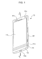
- Fig. 1 illustrates the structure of a terminal device of an example of an embodiment according to the present disclosure.
- a terminal device 100 illustrated in Fig. 1 is a mobile phone terminal device, which is a so-called smart phone.
- the terminal device 100 includes a first housing 101 and a second housing 102.
- the first housing 101 includes a display unit 110 and electronic circuitry.
- the display unit 110 is disposed in a surface of the first housing 101, and the electronic circuitry, which is part of the mobile phone terminal device, is disposed inside the first housing 101.
- the display unit 110 uses a display panel such as a liquid crystal display panel or an organic EL (electroluminescence) display panel.
- a touch panel is incorporated in the display panel provided in the display unit 110.
- a transparent member 120 is connected to a lower portion 101a of the first housing 101, and the second housing 102 is connected to a lower portion of the transparent member 120.
- the transparent member 120 extends along the entire lateral width of the first housing 101 and the second housing 102.
- the first housing 101 and the second housing 102 are spaced apart by a gap of a certain distance therebetween in the terminal device 100.
- the second housing 102 is a small component that houses an antenna, a microphone, and a vibrator.
- a microphone mounting portion 102a is formed at a lower end portion of the second housing 102.
- a speaker mounting portion 101b and a camera mounting portion 101c are disposed at an upper end portion of the first housing 101.
- a speaker and a camera unit are disposed in the respective mounting portions 101b and 101c inside the first housing 101.
- the touch panel provided in the display unit 110 has characteristics by which a touch is detected in an area slightly larger than a display area of the display panel near the lower portion 101a of the first housing 101. For example, even when a user touches a position that is slightly under an image display area of the display panel and is in contact with the transparent member 120, the operation by the user is detected by the touch panel.
- the terminal device 100 includes the first housing 101 and the second housing 102. Some electronic components are disposed in the second housing 102.
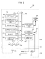
- the terminal device 100 which is a mobile phone terminal, includes an antenna 501 and an antenna member 170 as antennas that transmit and receive electric waves to and from a radiotelephone base station.
- the antenna 501 is disposed in the first housing 101 and the antenna member 170 is disposed in the second housing 102.
- An antenna in the antenna member 170 and the antenna 501 are connected to a communication processing unit 502.
- the communication processing unit 502 performs radio communication with a radiotelephone base station under the control of a control unit 510.
- voice communication the communication processing unit 502 supplies voice data included in received data to a voice processing unit 506.
- the voice processing unit 506 decodes the supplied voice data to obtain an analog voice signal.
- the analog voice signal obtained in the voice processing unit 506 is supplied to a speaker 507.
- the speaker 507 outputs voice in accordance with the received analog voice signal.
- a microphone 181 that picks up voice is also provided.
- the voice signal output from the microphone 181 is supplied to the voice processing unit 506.
- the microphone 181 is disposed in the second housing 102.
- the voice processing unit 506 encodes the received voice signal into voice data using a specified encoding scheme.
- the voice processing unit 506 supplies the encoded voice data to the communication processing unit 502.
- the communication processing unit 502 converts the supplied voice data into a packet format for transmission and modulates the data for transmission.
- the communication processing unit 502 supplies the modulated transmission signal to the antenna 501 or the antenna in the antenna member 170 and the modulated transmission signal is then radiated as radio waves.
- Processing units such as a communication processing unit 502 and a voice processing unit 506 transmit and receive control data to and from the control unit 510 through a control line 530 and transmit data through a data line 540.
- the terminal device 100 also includes the display unit 110 and an operation unit 504. Display on the display unit 110 is performed under the control of the control unit 510.
- the display unit 110 displays information necessary for an incoming or outgoing call, information about an email such as a destination address and a message, an image obtained through an Internet connection, an image picked up by a camera unit 522, information obtained through execution of a variety of functions which the terminal device 100 has, and so forth.
- the operation unit 504 includes operation keys disposed in the terminal device 100 and the touch panel disposed in the display unit 110. The operation unit 504 supplies instructions issued by operations performed by the user to the control unit 510. When the control unit 510 is supplied with data generated by detection of a touch operation in the touch panel, the control unit 510 determines what position is touched in an image displayed on the display unit 110 and performs a process in accordance with the touch operation.
- the control unit 510 includes a microprocessor and performs communication control, voice processing and control of voice processing, image processing and control of image processing, and so forth.
- the control unit 510 is connected to a memory 505 through the control line 530 and the data line 540.
- the control unit 510 reads data and programs stored in the memory 505.
- the terminal device 100 includes the camera unit 522.
- the camera unit 522 picks up images under the control of an image pickup control unit 521.
- Still image data or moving image data obtained through an image pickup operation using the camera unit 522 is stored in the memory 505.
- the terminal device 100 also includes a vibrator drive unit 508.
- the vibrator drive unit 508 supplies a drive signal to a vibrator 182, which is disposed in the second housing 102, in accordance with an instruction from the control unit 510.
- the drive signal is supplied to the vibrator 182, the vibrator 182 starts up and vibrates the terminal device 100.
- the terminal device 100 includes an illumination drive unit 509.
- the illumination drive unit 509 drives three light emitting diodes 161a, 161b, and 161c, which illuminate transparent member 120, in accordance with an instruction form the control unit 510. States of illumination using the light emitting diodes 161a, 161b, and 161c will be described later.
- Fig. 3 is an exploded view illustrating members disposed near the transparent member 120 inside the first housing 101 and the second housing 102.
- a supporting member 130 is mounted on an upper side of the transparent member 120 and a supporting member 140 is mounted on a lower side of the transparent member 120.
- the supporting member 130 and the supporting member 140 are formed by molding white resin or other opaque resin.
- the transparent member 120 and the supporting members 130 and 140 are integrally formed by molding.
- the upper supporting member 130 is housed in the first housing 101, and the lower supporting member 140 is housed in the second housing 102.
- Each of the transparent member 120 and the supporting members 130 and 140 illustrated in Fig. 3 is formed by bonding a front member and a rear member to each other.
- the details of a structure in which the transparent flexible substrate 200 is surrounded will be described later.
- a circuit substrate 160 is mounted on the supporting member 130, which is disposed on the upper side of the transparent member 120.
- a circuit substrate 180 and the antenna member 170 are mounted on the supporting member 140, which is disposed on the lower side of the transparent member 120.
- the microphone 181 and the vibrator 182 are mounted on the circuit substrate 180.
- the circuit substrate 160 disposed above the transparent member 120 are electrically connected to the antenna 170 and the circuit substrate 180 disposed below the transparent member 120 through a wiring pattern on the transparent flexible substrate 200. The details of the state of the electrical connection will be described later.
- the transparent member 120 has three transparent extended portions 123a, 123b, and 123c that protrude upward.
- the circuit substrate 160 to be mounted on the supporting member 130 includes the three light emitting diodes 161a, 161b, and 161c, which are respectively disposed at positions so as to be adjacent to the transparent extended portions 123a, 123b, and 123c in an assembled state.
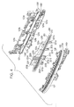
- Fig. 4 illustrates the details of the structure in which the transparent member 120 surrounds the transparent flexible substrate 200.
- the transparent member 120 is formed by bonding a front transparent member 120f and a rear transparent member 120r to each other.
- the front side of Fig. 4 is a rear surface of the terminal device 100 and the rear side of Fig. 4 is a front surface of the terminal device 100.
- a rear surface 127 (a surface on the front side in Fig. 4 ) of the rear transparent member 120r is a curved surface along the shapes of rear surfaces of the first housing 101 and the second housing 102.
- the front transparent member 120f and the rear transparent member 120r are formed by molding, for example, transparent acryl resin.
- a front supporting member 130f is integrally molded with the front transparent member 120f on the upper side of the front transparent member 120f.
- a front supporting member 140f is integrally molded with the front transparent member 120f on the lower side of the front transparent member 120f.
- a rear supporting member 130r is integrally molded with the rear transparent member 120r on the upper side of the rear transparent member 120r.
- a rear supporting member 140r is integrally molded with the rear transparent member 120r on the lower side of the rear transparent member 120r.
- the front supporting members 130f and 140f which are integrally molded with the front transparent member 120f on the upper and lower sides of the front transparent member 120f, respectively, and the rear supporting members 130r and 140r, which are integrally molded with the rear transparent member 120r on the upper and lower sides of the rear transparent member 120r, respectively, are formed by molding colored resin such as white resin. In the description below, it is assumed that the front supporting members 130f and 140f and the rear supporting members 130r and 140r are colored white.
- the transparent members 120f and 120r and the white supporting members 130f, 130r, 140f, and 140r are integrally molded by, for example, two-color molding (double mode). That is, in order to mold resin, white resin is initially charged into the mold so as to mold the supporting members 130f, 130r, 140f, and 140r. After that, transparent resin is charged into the mold so as to mold the transparent members 120f and 120r which are transparent while the components formed by molding the white resin are still left in the mold.
- the transparent members are initially molded, it is only an example and the white supporting members may be initially molded.
- the three transparent extended portions 123a, 123b, and 123c which have been described with reference to Fig. 3 , are integrally formed of the transparent resin with the front transparent member 120f on the upper side of the front transparent member 120f near a mating surface 121 of the front transparent member 120f.
- the transparent extended portions 123a, 123b, and 123c each have a corresponding one of transparent protrusions 124a, 124b, and 124c formed in the middle of each of the transparent extended portions 123a, 123b, and 123c.
- the transparent extended portions 123a, 123b, and 123c are thin components and would be easily damaged as individual components.
- the front supporting member 130f supports the transparent extended portions 123a, 123b, and 123c, thereby maintaining the strength of the transparent extended portions 123a, 123b, and 123c.
- three printed patterns 121a, 121b, and 121c are formed on the mating surface 121 of the front transparent member 120f.
- Each of the printed patterns 121a, 121b, and 121c simply graphically indicates an operation key formed at a position where each of the printed patterns 121a, 121b, and 121c is printed.
- the printed pattern 121a indicates a graphic of a back key
- the printed pattern 121b indicates a graphic of a home key
- the printed pattern 121c indicates a graphic of a menu key.
- These printed patterns 121a to 121c are printed in colors that appear nearly transparent, and become clearly visible when illumination, which will be described later, is performed.
- the transparent flexible substrate 200 is interposed therebetween and transparent adhesive 401 ( Fig. 6 ) is applied.
- transparent adhesive 401 is used for bonding, it is only an example and adhesive tape may be used for bonding. Alternatively, the adhesive 401 may be used together with the adhesive tape.
- the transparent flexible substrate 200 is formed of a resin material having high transparency such as PET (Polyethylene terephthalate).
- the transparent flexible substrate 200 has a belt portion 201, lower protrusions 202a, 202b, and 202c, and an upper protrusion 203.
- the belt portion 201 is interposed between the front transparent member 120f and the rear transparent member 120r.
- the lower protrusions 202a, 202b, and 202c protrude downward from the belt portion 201.
- the upper protrusion 203 protrudes upward from the belt portion 201.
- a transparent electrode pattern 210 is disposed on the belt portion 201.
- Pads 221a to 221g and 222a to 222g, which are connected to the transparent electrode pattern 210, are disposed in the protrusions 202a, 202b, 202c, and 203. The details of the structure including an electrode pattern provided on the transparent flexible substrate 200 will be described later.
- Fig. 5 is a sectional view of a state in which components are arranged in the terminal device 100. As illustrated cutting plane line V-V in Fig. 1 , Fig. 5 illustrates a vertical section taken at substantially the center of the terminal device 100.
- the transparent flexible substrate 200 is interposed between the front transparent member 120f and the rear transparent member 120r.
- the transparent extended portion 123b of the front transparent member 120f extends upward along the supporting member 130f.
- the transparent protrusion 124b formed in the middle of the transparent extended portion 123b is disposed near the light emitting diode 161b mounted on the circuit substrate 160.
- the printed pattern 121b (see Fig. 4 ) is formed on the mating surface 121.
- the printed pattern 121b becomes clearly visible by light emitted from the light emitting diode 161b.
- the other printed patterns 121a and 121c also become clearly visible by light emitted from the light emitting diodes 161a and 161c.
- the front transparent member 120f contacts an edge 131 of the white front supporting member 130f at an upper end portion thereof and an edge 141 of the white front supporting member 140f at a lower end portion thereof.
- the rear transparent member 120r contacts an edge 132 of the white rear supporting member 130r at an upper end portion thereof and an edge 142 of the white rear supporting member 140r at a lower end portion thereof.
- Fig. 6 illustrates a state in which the front transparent member 120f and the rear transparent member 120r are mated with each other.
- the front supporting member 130f and the rear supporting member 130r are removed in Fig. 6 .
- the mating surface 121 of the front transparent member 120f and the mating surface 122 of the rear transparent member 120r are bonded to each other with the transparent adhesive 401 applied into the gap therebetween.
- the transparent flexible substrate 200 is disposed between both of the mating surfaces 121 and 122.
- the belt portion 201 of the transparent flexible substrate 200 is interposed and hidden between the mating surfaces 121 and 122 while the upper protrusion 203 extends upward from the mating surfaces 121 and 122.
- an end surface 125 of the front transparent member 120f and an end surface 126 of the rear transparent member 120r are polished.
- the transparent members 120f and 120r are formed by molding resin, gates for injecting resin are formed on the end surfaces 125 and 126. This polishing process is performed in order to remove the gates, and accordingly, to align both the end surfaces 125 and 126 with each other on a single plane.
- Fig. 7 illustrates an example arrangement of electrodes on the transparent flexible substrate 200.
- the transparent flexible substrate 200 which is formed of a transparent resin material such as PET, has the belt portion 201 interposed between the front transparent member 120f and the rear transparent member 120r as described above.
- the transparent electrode pattern 210 which is a transmissive region, is arranged in the belt portion 201.
- the transparent electrode pattern 210 is formed of electrodes having very small widths, the electrodes being arranged so as to have a mesh-like shape. This makes most of the transparent electrode pattern 210 transmissive, thereby realizing an electrode pattern having a substantially transparent appearance.
- the electrodes arranged in the mesh-like shape are equally spaced apart from one another. Thus, the mesh-like transparent electrode pattern 210 is not completely transparent.
- the transparent electrode pattern 210 becomes weakly visible when the transparent electrode pattern 210 is illuminated by comparatively bright light.
- a conductive region 220 is arranged in the transparent flexible substrate 200.
- the conductive region 220 includes a transmissive region (transparent electrode pattern) 210 and non-transmissive regions (non-transparent electrodes) 223 and 224.
- the mesh-like transparent electrode pattern 210 which is the transmissive region, is divided into a plurality of electrodes by a plurality of vertically (in the vertical direction of the terminal device 100) extending pattern gap portions 211. Some of the plurality of electrodes are utilized as wiring line portions 212a to 212g. The pattern gap portions 211 are also formed at positions that are not utilized as the wiring line portions 212a to 212g.
- the transparent electrode pattern 210 When the transparent electrode pattern 210 is cut by the pattern gap portions 211, four wide width portions 210a, 210b, 210c, and 210d are formed. Out of the four wide width portions 210a to 210d, three wide width portions 210a, 210b, and 210d are bonded to positions on which the printed patterns 121a, 121b, and 121c are printed on the mating surface 121 ( Fig. 4 ) of the front transparent member 120f.
- the wiring line portions 212a to 212g of the transparent electrode pattern 210, through which electricity flows, are electrically connected to non-transparent electrodes 223a to 223g and 224a to 224g formed in the non-transmissive regions 223 and 224.
- the non-transparent electrodes 223a to 223g and 224a to 224g of the non-transmissive regions 223 and 224 are formed by a typical electrically conductive material such as copper arranged on the transparent flexible substrate 200. Electrically conductive portions of the non-transparent electrodes 223a to 223g and 224a to 224g have the pads 221a to 221g and 222a to 222g, which have exposed electrodes.
- the pads 221a to 221g and 222a to 222g are plated with, for example, gold.
- a specific connection states of the wiring line portions are described as follows. That is, for example, the wiring line portion 212a of the transparent electrode pattern 210 is connected to the non-transparent electrode 223a in the lower portion of the transparent flexible substrate 200 and connected to the non-transparent electrode 224a in the upper portion of the transparent flexible substrate 200.
- the lower non-transparent electrode 223a has the pad 221a and the upper non-transparent electrode 224a has the pad 222a.
- the wiring line portion 212b of the transparent electrode pattern 210 is connected to the non-transparent electrode 223b in the lower portion of the transparent flexible substrate 200 and connected to the non-transparent electrode 224b in the upper portion of the transparent flexible substrate 200.
- the lower non-transparent electrode 223b has the pad 221b and the upper non-transparent electrode 224b has the pad 222b.
- These two wiring line portions 212a and 212b are used as wiring for the antenna incorporated in the antenna member 170.
- the antenna member 170 in the second housing 102 is connected to the communication processing unit 502 ( Fig. 2 ) in the first housing 101 through the transparent wiring line portions 212a and 212b.
- the three wiring line portions 212c, 212d, and 212e which are arranged side by side, are respectively connected to the non-transparent electrodes 223c, 223d, and 223e in the lower portion of the transparent flexible substrate 200 and respectively connected to the non-transparent electrodes 224c, 224d, and 224e in the upper portion of the transparent flexible substrate 200.
- the lower non-transparent electrodes 223c, 223d, and 223e respectively have the pads 221c, 221d, and 221e
- the upper non-transparent electrodes 224c, 224d, and 224e respectively have the pads 222c, 222d, and 222e.
- These three wiring line portions 212c, 212d, and 212e are used as wiring for microphone 181.
- the voice signal obtained using the microphone 181 in the second housing 102 is supplied to a voice processing circuit (not shown) in the first housing 101.
- the wiring line portions 212f and 212g are respectively connected to the non-transparent electrodes 223f and 223g in the lower portion of the transparent flexible substrate 200 and respectively connected to the non-transparent electrodes 224f and 224g in the upper portion of the transparent flexible substrate 200.
- the lower non-transparent electrodes 223f and 223g respectively have the pads 221f and 221g
- the upper non-transparent electrodes 224f and 224g have the pads 222f and 222g.
- These two wiring lines 212f and 212g are used as wiring that supplies the drive signal to the vibrator 182.
- Part of the transparent electrode pattern 210 not used as wiring is disposed between the two wiring lines 212f and 212g.
- the wiring lines 212f and 212g are formed using the wide width portions 210c and 210d of the transparent electrode pattern 210.
- the vibrator 182 is a component that vibrates the terminal device 100 with a vibrating element being vibrated by rotation or the like of a motor. Accordingly, a comparatively large current needs to flow in order to drive the vibrator 182. With the transparent wiring lines 212f and 212g using the wide width portions 210c and 210d, a required level of the current can be supplied to the vibrator 182.
- Fig. 8 illustrates the section of a non-conductive region 261, of which the transparent electrode pattern 210 other than the wiring line portions 212, the pattern gap portions 211, and the like are formed, a conductive region 262, of which the wiring line portions 212 and the non-transmissive regions 223 and 224 are formed, and a pad region 263 in which the pads are disposed. The electrode of each pad is exposed.
- the structure of the non-conductive region 261 is initially described.
- the non-conductive region 261 of the transparent flexible substrate 200 has a structure in which a cover material 255 is stacked on a base material 251 formed of transparent resin (PET or the like) with a transparent bonding layer 252 therebetween.
- the cover material 255 is also formed of transparent resin such as PET.
- This region is a transparent region, in which a copper foil 253 used for the conductive region 262 and the pad region 263 are not present.
- the conductive region 262 of the transparent flexible substrate 200 is formed as follows. That is, the mesh-like copper foil 253 is stacked on the base material 251 with the transparent bonding layer 252 therebetween. Copper oxide films 256 and 257 are formed on upper and lower sides of the copper foil 253. Furthermore, the cover material 255 is stacked on them with the transparent bonding layer 252 therebetween.
- the conductive region 262 decreases light reflected by copper due to the black-colored copper oxide films 256 and 257, thereby making the wiring line portions 212a to 212g formed of the copper foil 253 difficult to be visually recognized from an external area. Surfaces of the copper oxide films 256 and 257 may be roughened to irregularly reflect light, thereby making the wiring line portions 212a to 212g be more difficult to be visually recognized from an external area.
- the pad region 263 of the transparent flexible substrate 200 is formed as follows. That is, the copper foil 253 is stacked on the base material 251 with the copper oxide film 256 and the transparent bonding layer 252 therebetween. A nickel-plated layer 258 and a gold-plated layer 259 are stacked on the copper foil 253. The gold-plated layer 259 is exposed in the surface.
- the non-conductive region 261, the conductive region 262, and the pad region 263 are formed on the single transparent flexible substrate 200 in a continuous manner using the copper foil 253 and other common materials. That is, when seen in a section, for example, along line A-A' in Fig. 7 , the non-transparent electrode 224, which is formed of the conductive region 262, is disposed adjacent to the pad, which is formed of the pad region 263. The wiring line portion 212c, which is formed of the conductive region 262, is disposed adjacent to the non-transparent electrode 224.
- the transparent electrode pattern 210 other than the wiring line portion 212, the transparent electrode pattern 210 being formed of the non-conductive region 261, is disposed adjacent to the wiring line portion 212c.
- the wiring line portion 212c, which is formed of the conductive region 262 and the transparent electrode pattern 210 other than the wiring line 212, the transparent electrode pattern 210 being formed of the non-conductive region 261 are repeatedly disposed in accordance with the number of the mesh cells.
- Fig. 9 illustrates the relationship between the width of the wiring line portion of the transparent electrode pattern 210 formed of the mesh-like electrode in the transparent flexible substrate 200 and the current allowed to flow in the mesh-like wiring line portion. As illustrated in Fig. 9 , as the width increases, the current value allowed to flow increases. In Fig. 9 , the characteristic is represented in a stepwise manner because of the mesh-like shape of the wiring line portion. That is, as the number of cells of the mesh increases one by one, the current increases.
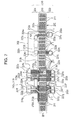
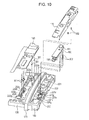
- Fig. 10 is an exploded view illustrating circuit substrates and members connected to the pads 221a to 221g, and 222a to 222g of the transparent flexible substrate 200 surrounded by the transparent member 120.
- the supporting member 130 is integrally molded on the upper side (left in Fig. 10 ) of the transparent member 120
- the supporting member 140 is integrally molded on the lower side of (right in Fig. 10 ) the transparent member 120.
- the supporting member 130 is housed in the first housing 101 illustrated in Fig. 1
- the supporting member 140 is housed in the second housing 102 illustrated in Fig. 1
- the transparent member 120 connects the two housings 101 and 102 to each other.
- the transparent flexible substrate 200 illustrated in Fig. 7 is interposed between the front transparent member 120f and the rear transparent member 120r, which are part of the transparent member 120.
- the pads 221a to 221g and 222a to 222g are exposed from the supporting members 130 and 140.
- the pads 221a and 221b are hidden by pin holders 231 and 232 provided on the supporting member 140.
- the pads 221a and 221b in the pin holders 231 and 232 of the supporting member 140 are connected to feeding points of the antenna member 170 through pins 302.
- the pads 221c, 221d, and 221e are connected to the microphone 181 on the circuit substrate 180 through the pins 302.
- the pads 221f and 221g are connected to the vibrator 182 on the circuit substrate 180 through the pins 302.
- the pins 302 are electrically conductive components having a spring therein.
- the pins 302 connect the pads 221a to 221g to components in an electrically stable manner.
- the pads 222a to 222g which are disposed on the supporting member 130 side, are connected to the conductive portions (not shown) of the circuit substrate 160 through plate springs 301. With the plate springs 301 being provided, the pads 222a to 222g are electrically stably connected to the circuit substrate 160.
- the transparent wiring line portions 212a to 212g which are disposed on the transparent flexible substrate 200 illustrated in Fig. 7 , are used to electrically connect the circuit substrate 160 disposed in the first housing 101 to the antenna member 170, the microphone 181, and the vibrator 182 disposed in the second housing 102 as illustrated in Fig. 10 .
- the circuitry in the first housing 101 connected through the transparent member 120 is electrically connected to electronic components in the second housing 102.
- radio signals are transmitted and received using the antenna member 170 in the second housing 102, and the antenna is disposed at a preferable lower end position.
- the microphone 181 is disposed in the second housing 102 at the lower end of the terminal device 100.
- the microphone 181 can be disposed at a preferable lower end position.
- the vibrator 182 can be disposed at the lower end of the terminal device 100, which is a position suitable for vibrating the terminal device 100.
- the amount of current allowed to flow in the transparent electrode pattern is small compared to a conductive portion formed typically of copper wires or the like.
- the wide width portions 210c and 210d are used for the transparent wiring lines 212f and 212g that supply a comparative high current drive signal to the vibrator 182, thereby allowing a comparatively high current to flow.
- the transparent wiring lines 212a and 212b for connecting the antenna member 170 are disposed at positions so as to be comparatively spaced apart from the other wiring lines 212c to 212g, and a number of the pattern gap portions 211 are formed.
- the transparent electrode pattern 210 is finely divided by a number of the pattern gap portions 211 with a degree of distances. By doing this, the transparent electrodes of the transparent electrode pattern 210 do not have a large electrical capacitance that can affect the antenna characteristics. Thus, unnecessary capacitors are not arranged near connection paths of the antenna, thereby realizing preferable antenna characteristics.
- the arrangement state and the number of the pattern gap portions 211 illustrated in Fig. 7 are only an example.
- electrical capacitance of each transparent electrode is suitably selected in accordance with a frequency band transmitted and received by the antenna member 170.
- the non-transparent wiring lines are formed so as to be continuous with the mesh-like transparent electrode pattern, and pads are provided on the non-transparent wiring lines.
- the transparent flexible substrate 200 can be electrically connected to external circuitry in a preferable manner. That is, since the mesh-like transparent electrode pattern is a pattern including fine wiring lines, the mesh-like transparent electrode pattern is not easily directly connected to the external circuitry in a stable manner.
- the non-conductive region 261, the conductive region 262, and the pad region 263 are formed, thereby allowing preferable electrical connection to be realized using the pads of the pad region 263.
- the light emitting diodes 161a, 161b, and 161c are disposed near the transparent member 120 of the terminal device 100.
- the display unit 110 substantially entirely covers a surface of the first housing 101.
- the touch panel provided in the display unit 110 has a sensitivity that detects a touch made at positions down to the lower portion 101a of the first housing.
- the three light emitting diodes 161a, 161b, and 161c are disposed in the lower portion 101a of the first housing 101.
- the user holding the terminal device 100 touches a position near positions where the light emitting diodes 161a, 161b, and 161c are disposed on the surface of the housing 101.
- the touch panel provided in the display unit 110 detects the touching operation and operates in accordance with the touching operation.
- the light emitting diode 161a, 161b, or 161a near a position where the touching operation is detected emits light.
- the mating surface 121 of the transparent member 120 is illuminated and the corresponding printed patterns 121a, 121b, and 121c ( Fig. 4 ) formed at the illuminated positions become clearly visible.
- the three light emitting diodes 161a, 161b, and 161c may separately emit light in accordance with a touch detected at positions where the light emitting diode 161a, 161b and 161c are disposed.
- the three light emitting diodes 161a, 161b, and 161c may simultaneously emit light when a touch is detected at a position where any one of the light emitting diode 161a, 161b and 161c is disposed.
- the light emitting diodes 161a, 161b, and 161c may emit light in accordance with an operating mode of the terminal device 100 independently of detection of a touch.
- the position where the transparent member 120 is disposed functions as touch keys with illumination.
- the functions assigned to the keys are indicated by the printed patterns 121a, 121b, and 121c.
- the positions where the printed patterns 121a, 121b, and 121c are formed are the wide width portions 210c, 210b, and 210d of the transparent electrode pattern 210 of the transparent flexible substrate 200 as illustrated in Fig. 7 .
- the pattern gap portions 211 are not formed at positions where the printed patterns 121a, 121b, and 121c are illuminated. This prevents a situation in which unnecessary linearly shaped portions become visible because of illumination at positions where the pattern gap portions 211 are formed.
- Fig. 12 illustrates the relationship between the positions illuminated by the three light emitting diodes 161a, 161b, and 161c and the arrangement state of the wide width portions 210a, 210b and 210d of the transparent electrode pattern 210 of the transparent flexible substrate 200.
- the wide width portions 210a, 210b and 210d are illuminated and the pattern gap portions 211 are not illuminated by intense light. Thus, unnecessary lines are not visible at the illuminated positions.
- the transparent member 120 contacts the edges 131 and 132 of the white supporting member 130 at the upper portion thereof and the edges 141 and 142 of the white supporting member 140 at the lower end portion thereof.
- light introduced from the light emitting diodes 161a, 161b, and 161c into the transparent member 120 is efficiently supplied to the front and rear surfaces without leaking through an area above or below the transparent member 120.
- preferable illumination can be realized.
- the copper oxide films 256 and 257 are formed on the copper foil 253 of the conductive region in the transparent flexible substrate 200.
- the copper oxide films 256 and 257 are formed on the copper foil 253 of the conductive region in the transparent flexible substrate 200.
- a housing of a portable audio player device may include a first housing and second housing.
- the first and second housings are connected to each other using a transparent member, and a transparent member holding mechanism of the present disclosure is applied to the portable audio player device.
- the antenna, the microphone, and the vibrator are disposed in the second housing 102 and connected to the circuitry in the first housing 101 through the transparent electrodes.
- other electronic components may be disposed in the second housing 102.
- the electronic components disposed are connected to the circuitry in the first housing 101 through the transparent electrode pattern of the transparent flexible substrate 200.
- the touch panel on the first housing 101 side is used as a touch detection sensor in order to make an area near the transparent member 120 function as touch keys.
- a touch detection sensor may be disposed, for example, in the second housing 102.
- the transparent member 120 is illuminated when a touch made on the surface of the second housing 102 is detected.
- the touch detection sensor in the second housing 102 may be connected to the circuitry in the first housing 101 through the transparent electrode pattern of the transparent flexible substrate 200.
- the mesh-like transparent electrode pattern 210 is disposed on the transparent flexible substrate 200.
- the conductive portion on the first housing 101 side and the conductive portion on the second housing 102 side may be connected by a transparent electrode portion formed of one or plurality of linearly shaped lines.
- a conductive material such as copper are arranged so as to form a thin mesh-like shape, thereby allowing the transparent electrode pattern 210 to appear substantially transparent.
- the transparent electrode pattern may use a transparent conductive material such as ITO (indium tin oxide).
- the present disclosure may include (1) an information processing apparatus comprising: a first housing; a second housing; a transparent member disposed between the first and second housings; and a transparent substrate including a transmissive electrode area having a wiring line portion electrically connecting an interior of the first housing and an interior of the second housing, the wiring line portion having a width set based on a current flow through the wire line portion.
Landscapes
- Engineering & Computer Science (AREA)
- Theoretical Computer Science (AREA)
- Computer Hardware Design (AREA)
- General Engineering & Computer Science (AREA)
- Human Computer Interaction (AREA)
- Physics & Mathematics (AREA)
- General Physics & Mathematics (AREA)
- Signal Processing (AREA)
- Microelectronics & Electronic Packaging (AREA)
- Telephone Set Structure (AREA)
Abstract
A transparent substrate including a transmissive electrode area including a plurality of wiring line portions arranged side by side on a substrate formed of a transparent material, a width of each of the wiring line portions being set in accordance with a current to flow through the wiring line portion; and a non-transmissive electrode area disposed on the substrate, the non-transmissive electrode being connected to the wiring line portions of the transmissive electrode area.
Description
- The present application claims the benefit of the earlier filing date of
U.S. Provisional Patent Application Serial No. 61/580,571 filed on December 27, 2011 - The present disclosure relates to a terminal device and a transparent substrate.
- Today, there are electronic devices having a housing, part of which is transparent so as to realize well-designed electronic devices.
- Japanese Patent Application Publication No.
2005-267897 - Generally, when a portion of a housing is transparent, components or the like are not disposed in the transparent portion of the housing. That is, when, for example, electrical wiring is disposed in the transparent portion, the wiring is visible from the outside. It is an undesirable situation. In related art, transparent electrodes, which are electrodes formed of a light transmissive material, are in practical use and applied to liquid crystal display panels, touch panels, and the like.
- However, it is difficult for transparent electrodes to allow a large current to flow therethrough compared to typical wiring materials such as copper and aluminum, and accordingly, it is difficult to use transparent electrodes as part of general wiring materials.
- Thus, when part of a housing is transparent in the related art, wiring routed in the housing has not been disposed at positions where the housing is transparent.
- Inventors recognize that it is desirable that part of the housing of the terminal device be made transparent, and that wiring be preferably disposed at the transparent part.
- According to a first exemplary embodiment, the disclosure is directed to an information processing apparatus comprising: a first housing; a second housing; a transparent member disposed between the first and second housings; and a transparent substrate including a transmissive electrode area having a wiring line portion electrically connecting an interior of the first housing and an interior of the second housing, the wiring line portion having a width set based on a current flow through the wire line portion.
- According to another exemplary embodiment, the disclosure is directed to a transparent substrate including a transmissive electrode area including a plurality of wiring line portions arranged side by side on a substrate formed of a transparent material, a width of each of the wiring line portions being set in accordance with a current to flow through the wiring line portion; and a non-transmissive electrode area disposed on the substrate, the non-transmissive electrode being connected to the wiring line portions of the transmissive electrode area.
- According to the embodiment of the present disclosure, the widths of wiring components disposed as the transmissive electrode area are set in accordance with currents to flow through the wiring line portions. Thus, the wiring line portions through which a comparatively high currents need to flow can be preferably disposed as the transmissive electrode area.
- Various respective aspects and features of the invention are defined in the appended claims.
- Combinations of features from the dependent claims may be combined with features of the independent claims as appropriate and not merely as explicitly set out in the claims.
- Embodiments of the invention will now be described with reference to the accompanying drawings, throughout which like parts are referred to by like references, and in which:
-
Fig. 1 is a perspective view illustrating an example of the shape of a terminal device of an embodiment according to the present disclosure. -
Fig. 2 is a block diagram illustrating an example of the structure of the terminal device of the embodiment according to the present disclosure. -
Fig. 3 is an exploded perspective view illustrating part of the example terminal device illustrated inFig. 1 . -
Fig. 4 is an exploded perspective view illustrating members included in the example terminal device illustrated inFig. 1 . -
Fig. 5 is a sectional view of part of the example terminal device illustrated inFig. 1 taken along line V-V inFig. 1 . -
Fig. 6 is a perspective view illustrating members included in the example terminal device illustrated inFig. 1 . -
Fig. 7 is a plan view illustrating an example of a transparent substrate disposed in the example terminal device illustrated inFig. 1 . -
Fig. 8 is a sectional view of the example transparent substrate illustrated inFig. 7 . -
Fig. 9 is a characteristic chart of the transparent substrate. -
Fig. 10 is an exploded perspective view illustrating members included in the example terminal device illustrated inFig. 1 . -
Fig. 11 is a perspective view illustrating a state in which part of the example terminal device illustrated inFig. 1 is illuminated. -
Fig. 12 illustrates a state in which the transparent substrate is illuminated. - An example of a terminal device and a transparent member holding mechanism according to an embodiment of the present disclosure will be described hereafter with reference to the drawings in the following order.
- 1. Outer Shape of Terminal Device (
Fig. 1 ) - 2. Configuration of Terminal Device (
Fig. 2 ) - 3. Structure for Connecting First Housing to Second Housing (
Figs. 3 to 6 ) - 4. Connection Structure using Transparent Flexible Substrate (
Figs. 7 to 10 ) - 5. Illumination State of Transparent Portion (
Figs. 11 and12 ) - 6. Modifications
-
Fig. 1 illustrates the structure of a terminal device of an example of an embodiment according to the present disclosure. - A
terminal device 100 illustrated inFig. 1 is a mobile phone terminal device, which is a so-called smart phone. - The
terminal device 100 includes afirst housing 101 and asecond housing 102. Thefirst housing 101 includes adisplay unit 110 and electronic circuitry. Thedisplay unit 110 is disposed in a surface of thefirst housing 101, and the electronic circuitry, which is part of the mobile phone terminal device, is disposed inside thefirst housing 101. Thedisplay unit 110 uses a display panel such as a liquid crystal display panel or an organic EL (electroluminescence) display panel. A touch panel is incorporated in the display panel provided in thedisplay unit 110. - A
transparent member 120 is connected to alower portion 101a of thefirst housing 101, and thesecond housing 102 is connected to a lower portion of thetransparent member 120. Thetransparent member 120 extends along the entire lateral width of thefirst housing 101 and thesecond housing 102. Thus, thefirst housing 101 and thesecond housing 102 are spaced apart by a gap of a certain distance therebetween in theterminal device 100. Thesecond housing 102 is a small component that houses an antenna, a microphone, and a vibrator. - A
microphone mounting portion 102a is formed at a lower end portion of thesecond housing 102. - A
speaker mounting portion 101b and acamera mounting portion 101c are disposed at an upper end portion of thefirst housing 101. A speaker and a camera unit are disposed in therespective mounting portions first housing 101. - The touch panel provided in the
display unit 110 has characteristics by which a touch is detected in an area slightly larger than a display area of the display panel near thelower portion 101a of thefirst housing 101. For example, even when a user touches a position that is slightly under an image display area of the display panel and is in contact with thetransparent member 120, the operation by the user is detected by the touch panel. - Next, the configuration inside the
terminal device 100 will be described with reference toFig. 2 . - As described above, the
terminal device 100 includes thefirst housing 101 and thesecond housing 102. Some electronic components are disposed in thesecond housing 102. - The
terminal device 100, which is a mobile phone terminal, includes anantenna 501 and anantenna member 170 as antennas that transmit and receive electric waves to and from a radiotelephone base station. Theantenna 501 is disposed in thefirst housing 101 and theantenna member 170 is disposed in thesecond housing 102. An antenna in theantenna member 170 and theantenna 501 are connected to acommunication processing unit 502. - The
communication processing unit 502 performs radio communication with a radiotelephone base station under the control of acontrol unit 510. In voice communication, thecommunication processing unit 502 supplies voice data included in received data to avoice processing unit 506. Thevoice processing unit 506 decodes the supplied voice data to obtain an analog voice signal. The analog voice signal obtained in thevoice processing unit 506 is supplied to aspeaker 507. Thespeaker 507 outputs voice in accordance with the received analog voice signal. - A
microphone 181 that picks up voice is also provided. The voice signal output from themicrophone 181 is supplied to thevoice processing unit 506. Themicrophone 181 is disposed in thesecond housing 102. Thevoice processing unit 506 encodes the received voice signal into voice data using a specified encoding scheme. Thevoice processing unit 506 supplies the encoded voice data to thecommunication processing unit 502. Thecommunication processing unit 502 converts the supplied voice data into a packet format for transmission and modulates the data for transmission. Thecommunication processing unit 502 supplies the modulated transmission signal to theantenna 501 or the antenna in theantenna member 170 and the modulated transmission signal is then radiated as radio waves. - Processing units such as a
communication processing unit 502 and avoice processing unit 506 transmit and receive control data to and from thecontrol unit 510 through acontrol line 530 and transmit data through adata line 540. - The
terminal device 100 also includes thedisplay unit 110 and anoperation unit 504. Display on thedisplay unit 110 is performed under the control of thecontrol unit 510. Thedisplay unit 110 displays information necessary for an incoming or outgoing call, information about an email such as a destination address and a message, an image obtained through an Internet connection, an image picked up by acamera unit 522, information obtained through execution of a variety of functions which theterminal device 100 has, and so forth. Theoperation unit 504 includes operation keys disposed in theterminal device 100 and the touch panel disposed in thedisplay unit 110. Theoperation unit 504 supplies instructions issued by operations performed by the user to thecontrol unit 510. When thecontrol unit 510 is supplied with data generated by detection of a touch operation in the touch panel, thecontrol unit 510 determines what position is touched in an image displayed on thedisplay unit 110 and performs a process in accordance with the touch operation. - The
control unit 510 includes a microprocessor and performs communication control, voice processing and control of voice processing, image processing and control of image processing, and so forth. Thecontrol unit 510 is connected to amemory 505 through thecontrol line 530 and thedata line 540. Thecontrol unit 510 reads data and programs stored in thememory 505. - The
terminal device 100 includes thecamera unit 522. Thecamera unit 522 picks up images under the control of an imagepickup control unit 521. Still image data or moving image data obtained through an image pickup operation using thecamera unit 522 is stored in thememory 505. - The
terminal device 100 also includes avibrator drive unit 508. Thevibrator drive unit 508 supplies a drive signal to avibrator 182, which is disposed in thesecond housing 102, in accordance with an instruction from thecontrol unit 510. When the drive signal is supplied to thevibrator 182, thevibrator 182 starts up and vibrates theterminal device 100. - The
terminal device 100 includes anillumination drive unit 509. Theillumination drive unit 509 drives threelight emitting diodes transparent member 120, in accordance with an instruction form thecontrol unit 510. States of illumination using thelight emitting diodes - Next, a structure that connects the
first housing 101 to thesecond housing 102 using thetransparent member 120 will be described with reference toFigs. 3 to 6 . -
Fig. 3 is an exploded view illustrating members disposed near thetransparent member 120 inside thefirst housing 101 and thesecond housing 102. - As illustrated in
Fig. 3 , a supportingmember 130 is mounted on an upper side of thetransparent member 120 and a supportingmember 140 is mounted on a lower side of thetransparent member 120. The supportingmember 130 and the supportingmember 140 are formed by molding white resin or other opaque resin. Although the supportingmember 130 is separated from thetransparent member 120 inFig. 3 , thetransparent member 120 and the supportingmembers - The upper supporting
member 130 is housed in thefirst housing 101, and the lower supportingmember 140 is housed in thesecond housing 102. Each of thetransparent member 120 and the supportingmembers Fig. 3 is formed by bonding a front member and a rear member to each other. - A transparent
flexible substrate 200, on which transparent electrodes and so forth are formed, is surrounded by thetransparent member 120. The details of a structure in which the transparentflexible substrate 200 is surrounded will be described later. - A
circuit substrate 160 is mounted on the supportingmember 130, which is disposed on the upper side of thetransparent member 120. Acircuit substrate 180 and theantenna member 170 are mounted on the supportingmember 140, which is disposed on the lower side of thetransparent member 120. Themicrophone 181 and thevibrator 182 are mounted on thecircuit substrate 180. - The
circuit substrate 160 disposed above thetransparent member 120 are electrically connected to theantenna 170 and thecircuit substrate 180 disposed below thetransparent member 120 through a wiring pattern on the transparentflexible substrate 200. The details of the state of the electrical connection will be described later. - The
transparent member 120 has three transparentextended portions circuit substrate 160 to be mounted on the supportingmember 130 includes the threelight emitting diodes extended portions -
Fig. 4 illustrates the details of the structure in which thetransparent member 120 surrounds the transparentflexible substrate 200. As illustrated inFig. 4 , thetransparent member 120 is formed by bonding a fronttransparent member 120f and a reartransparent member 120r to each other. InFig. 4 , the front side ofFig. 4 is a rear surface of theterminal device 100 and the rear side ofFig. 4 is a front surface of theterminal device 100. A rear surface 127 (a surface on the front side inFig. 4 ) of the reartransparent member 120r is a curved surface along the shapes of rear surfaces of thefirst housing 101 and thesecond housing 102. - The front
transparent member 120f and the reartransparent member 120r are formed by molding, for example, transparent acryl resin. - A front supporting
member 130f is integrally molded with the fronttransparent member 120f on the upper side of the fronttransparent member 120f. A front supportingmember 140f is integrally molded with the fronttransparent member 120f on the lower side of the fronttransparent member 120f. Arear supporting member 130r is integrally molded with the reartransparent member 120r on the upper side of the reartransparent member 120r. Arear supporting member 140r is integrally molded with the reartransparent member 120r on the lower side of the reartransparent member 120r. The front supportingmembers transparent member 120f on the upper and lower sides of the fronttransparent member 120f, respectively, and therear supporting members transparent member 120r on the upper and lower sides of the reartransparent member 120r, respectively, are formed by molding colored resin such as white resin. In the description below, it is assumed that the front supportingmembers rear supporting members - The
transparent members members members transparent members - The three transparent
extended portions Fig. 3 , are integrally formed of the transparent resin with the fronttransparent member 120f on the upper side of the fronttransparent member 120f near amating surface 121 of the fronttransparent member 120f. The transparentextended portions transparent protrusions extended portions extended portions extended portions member 130f, thefront supporting member 130f supports the transparentextended portions extended portions - As illustrated in
Fig. 4 , three printedpatterns mating surface 121 of the fronttransparent member 120f. Each of the printedpatterns patterns pattern 121a indicates a graphic of a back key, the printedpattern 121b indicates a graphic of a home key, and the printedpattern 121c indicates a graphic of a menu key. These printedpatterns 121a to 121c are printed in colors that appear nearly transparent, and become clearly visible when illumination, which will be described later, is performed. - When the
mating surface 121 of thetransparent member 120f and amating surface 122 of thetransparent member 120r are bonded to each other, the transparentflexible substrate 200 is interposed therebetween and transparent adhesive 401 (Fig. 6 ) is applied. Although the adhesive 401 is used for bonding, it is only an example and adhesive tape may be used for bonding. Alternatively, the adhesive 401 may be used together with the adhesive tape. - The transparent
flexible substrate 200 is formed of a resin material having high transparency such as PET (Polyethylene terephthalate). The transparentflexible substrate 200 has abelt portion 201,lower protrusions upper protrusion 203. Thebelt portion 201 is interposed between the fronttransparent member 120f and the reartransparent member 120r. Thelower protrusions belt portion 201. Theupper protrusion 203 protrudes upward from thebelt portion 201. - A
transparent electrode pattern 210 is disposed on thebelt portion 201.Pads 221a to 221g and 222a to 222g, which are connected to thetransparent electrode pattern 210, are disposed in theprotrusions flexible substrate 200 will be described later. -
Fig. 5 is a sectional view of a state in which components are arranged in theterminal device 100. As illustrated cutting plane line V-V inFig. 1 ,Fig. 5 illustrates a vertical section taken at substantially the center of theterminal device 100. - As illustrated in
Fig. 5 , the transparentflexible substrate 200 is interposed between the fronttransparent member 120f and the reartransparent member 120r. The transparentextended portion 123b of the fronttransparent member 120f extends upward along the supportingmember 130f. Thetransparent protrusion 124b formed in the middle of the transparentextended portion 123b is disposed near thelight emitting diode 161b mounted on thecircuit substrate 160. Thus, when thelight emitting diode 161b emits light, the light strikes the transparentextended portion 123b. The light is introduced by the transparentextended portion 123b and illuminates an area near themating surface 121 of the fronttransparent member 120f. Here, as illustrated inFig. 4 , the printedpattern 121b (seeFig. 4 ) is formed on themating surface 121. The printedpattern 121b becomes clearly visible by light emitted from thelight emitting diode 161b. The other printedpatterns light emitting diodes - As can be seen from the sectional view in
Fig. 5 , the fronttransparent member 120f contacts anedge 131 of the whitefront supporting member 130f at an upper end portion thereof and anedge 141 of the whitefront supporting member 140f at a lower end portion thereof. The reartransparent member 120r contacts anedge 132 of the whiterear supporting member 130r at an upper end portion thereof and anedge 142 of the whiterear supporting member 140r at a lower end portion thereof. By doing this, when thelight emitting diodes 161a to 161c emit light, the light is supplied to the front and rear surfaces without leaking through an area above or below thetransparent member transparent members -
Fig. 6 illustrates a state in which the fronttransparent member 120f and the reartransparent member 120r are mated with each other. The front supportingmember 130f and therear supporting member 130r are removed inFig. 6 . Themating surface 121 of the fronttransparent member 120f and themating surface 122 of the reartransparent member 120r are bonded to each other with thetransparent adhesive 401 applied into the gap therebetween. The transparentflexible substrate 200 is disposed between both of the mating surfaces 121 and 122. In the state illustrated inFig. 6 , thebelt portion 201 of the transparentflexible substrate 200 is interposed and hidden between the mating surfaces 121 and 122 while theupper protrusion 203 extends upward from the mating surfaces 121 and 122. - In order to bond the front
transparent member 120f and the reartransparent member 120r to each other, anend surface 125 of the fronttransparent member 120f and anend surface 126 of the reartransparent member 120r are polished. When thetransparent members - Next, a structure that connects circuitry in the
first housing 101 to circuitry in thesecond housing 102 using the transparentflexible substrate 200 will be described with reference toFigs. 7 to 10 . -
Fig. 7 illustrates an example arrangement of electrodes on the transparentflexible substrate 200. The transparentflexible substrate 200, which is formed of a transparent resin material such as PET, has thebelt portion 201 interposed between the fronttransparent member 120f and the reartransparent member 120r as described above. Thetransparent electrode pattern 210, which is a transmissive region, is arranged in thebelt portion 201. Thetransparent electrode pattern 210 is formed of electrodes having very small widths, the electrodes being arranged so as to have a mesh-like shape. This makes most of thetransparent electrode pattern 210 transmissive, thereby realizing an electrode pattern having a substantially transparent appearance. The electrodes arranged in the mesh-like shape are equally spaced apart from one another. Thus, the mesh-liketransparent electrode pattern 210 is not completely transparent. Thetransparent electrode pattern 210 becomes weakly visible when thetransparent electrode pattern 210 is illuminated by comparatively bright light. - Next, the structure of the transparent
flexible substrate 200 illustrated inFig. 7 will be described. - As illustrated in
Fig. 7 , aconductive region 220 is arranged in the transparentflexible substrate 200. Theconductive region 220 includes a transmissive region (transparent electrode pattern) 210 and non-transmissive regions (non-transparent electrodes) 223 and 224. - The mesh-like
transparent electrode pattern 210, which is the transmissive region, is divided into a plurality of electrodes by a plurality of vertically (in the vertical direction of the terminal device 100) extendingpattern gap portions 211. Some of the plurality of electrodes are utilized aswiring line portions 212a to 212g. Thepattern gap portions 211 are also formed at positions that are not utilized as thewiring line portions 212a to 212g. - When the
transparent electrode pattern 210 is cut by thepattern gap portions 211, fourwide width portions wide width portions 210a to 210d, threewide width portions patterns Fig. 4 ) of the fronttransparent member 120f. - The
wiring line portions 212a to 212g of thetransparent electrode pattern 210, through which electricity flows, are electrically connected tonon-transparent electrodes 223a to 223g and 224a to 224g formed in thenon-transmissive regions non-transparent electrodes 223a to 223g and 224a to 224g of thenon-transmissive regions flexible substrate 200. Electrically conductive portions of thenon-transparent electrodes 223a to 223g and 224a to 224g have thepads 221a to 221g and 222a to 222g, which have exposed electrodes. Thepads 221a to 221g and 222a to 222g are plated with, for example, gold. - A specific connection states of the wiring line portions are described as follows. That is, for example, the
wiring line portion 212a of thetransparent electrode pattern 210 is connected to thenon-transparent electrode 223a in the lower portion of the transparentflexible substrate 200 and connected to thenon-transparent electrode 224a in the upper portion of the transparentflexible substrate 200. The lowernon-transparent electrode 223a has thepad 221a and the uppernon-transparent electrode 224a has thepad 222a. - The
wiring line portion 212b of thetransparent electrode pattern 210 is connected to thenon-transparent electrode 223b in the lower portion of the transparentflexible substrate 200 and connected to thenon-transparent electrode 224b in the upper portion of the transparentflexible substrate 200. The lowernon-transparent electrode 223b has thepad 221b and the uppernon-transparent electrode 224b has thepad 222b. - These two
wiring line portions antenna member 170. Theantenna member 170 in thesecond housing 102 is connected to the communication processing unit 502 (Fig. 2 ) in thefirst housing 101 through the transparentwiring line portions - The three
wiring line portions non-transparent electrodes flexible substrate 200 and respectively connected to thenon-transparent electrodes flexible substrate 200. The lowernon-transparent electrodes pads non-transparent electrodes pads - These three
wiring line portions microphone 181. The voice signal obtained using themicrophone 181 in thesecond housing 102 is supplied to a voice processing circuit (not shown) in thefirst housing 101. - The
wiring line portions non-transparent electrodes 223f and 223g in the lower portion of the transparentflexible substrate 200 and respectively connected to thenon-transparent electrodes flexible substrate 200. The lowernon-transparent electrodes 223f and 223g respectively have thepads non-transparent electrodes pads - These two
wiring lines vibrator 182. Part of thetransparent electrode pattern 210 not used as wiring is disposed between the twowiring lines wide width portions transparent electrode pattern 210. Thevibrator 182 is a component that vibrates theterminal device 100 with a vibrating element being vibrated by rotation or the like of a motor. Accordingly, a comparatively large current needs to flow in order to drive thevibrator 182. With thetransparent wiring lines wide width portions vibrator 182. - Next, the sectional structure of the transparent
flexible substrate 200 will be described with reference toFig. 8 . -
Fig. 8 illustrates the section of anon-conductive region 261, of which thetransparent electrode pattern 210 other than the wiring line portions 212, thepattern gap portions 211, and the like are formed, aconductive region 262, of which the wiring line portions 212 and thenon-transmissive regions pad region 263 in which the pads are disposed. The electrode of each pad is exposed. - The structure of the
non-conductive region 261 is initially described. Thenon-conductive region 261 of the transparentflexible substrate 200 has a structure in which acover material 255 is stacked on abase material 251 formed of transparent resin (PET or the like) with atransparent bonding layer 252 therebetween. Thecover material 255 is also formed of transparent resin such as PET. This region is a transparent region, in which acopper foil 253 used for theconductive region 262 and thepad region 263 are not present. - The
conductive region 262 of the transparentflexible substrate 200 is formed as follows. That is, the mesh-like copper foil 253 is stacked on thebase material 251 with thetransparent bonding layer 252 therebetween.Copper oxide films copper foil 253. Furthermore, thecover material 255 is stacked on them with thetransparent bonding layer 252 therebetween. Theconductive region 262 decreases light reflected by copper due to the black-coloredcopper oxide films wiring line portions 212a to 212g formed of thecopper foil 253 difficult to be visually recognized from an external area. Surfaces of thecopper oxide films wiring line portions 212a to 212g be more difficult to be visually recognized from an external area. - The
pad region 263 of the transparentflexible substrate 200 is formed as follows. That is, thecopper foil 253 is stacked on thebase material 251 with thecopper oxide film 256 and thetransparent bonding layer 252 therebetween. A nickel-platedlayer 258 and a gold-platedlayer 259 are stacked on thecopper foil 253. The gold-platedlayer 259 is exposed in the surface. - As can be seen from the section illustrated in
Fig. 8 , thenon-conductive region 261, theconductive region 262, and thepad region 263 are formed on the single transparentflexible substrate 200 in a continuous manner using thecopper foil 253 and other common materials. That is, when seen in a section, for example, along line A-A' inFig. 7 , thenon-transparent electrode 224, which is formed of theconductive region 262, is disposed adjacent to the pad, which is formed of thepad region 263. Thewiring line portion 212c, which is formed of theconductive region 262, is disposed adjacent to thenon-transparent electrode 224. Thetransparent electrode pattern 210 other than the wiring line portion 212, thetransparent electrode pattern 210 being formed of thenon-conductive region 261, is disposed adjacent to thewiring line portion 212c. In this manner, thewiring line portion 212c, which is formed of theconductive region 262, and thetransparent electrode pattern 210 other than the wiring line 212, thetransparent electrode pattern 210 being formed of thenon-conductive region 261, are repeatedly disposed in accordance with the number of the mesh cells. -
Fig. 9 illustrates the relationship between the width of the wiring line portion of thetransparent electrode pattern 210 formed of the mesh-like electrode in the transparentflexible substrate 200 and the current allowed to flow in the mesh-like wiring line portion. As illustrated inFig. 9 , as the width increases, the current value allowed to flow increases. InFig. 9 , the characteristic is represented in a stepwise manner because of the mesh-like shape of the wiring line portion. That is, as the number of cells of the mesh increases one by one, the current increases. - As can be seen from
Fig. 9 , use of thewide width portions vibrator 182 to flow. -
Fig. 10 is an exploded view illustrating circuit substrates and members connected to thepads 221a to 221g, and 222a to 222g of the transparentflexible substrate 200 surrounded by thetransparent member 120. As illustrated inFig. 10 , the supportingmember 130 is integrally molded on the upper side (left inFig. 10 ) of thetransparent member 120, and the supportingmember 140 is integrally molded on the lower side of (right inFig. 10 ) thetransparent member 120. As described before, in an assembled state, the supportingmember 130 is housed in thefirst housing 101 illustrated inFig. 1 , the supportingmember 140 is housed in thesecond housing 102 illustrated inFig. 1 , and thetransparent member 120 connects the twohousings - The transparent
flexible substrate 200 illustrated inFig. 7 is interposed between the fronttransparent member 120f and the reartransparent member 120r, which are part of thetransparent member 120. Thepads 221a to 221g and 222a to 222g are exposed from the supportingmembers Fig. 10 , thepads pin holders member 140. - The
pads pin holders member 140 are connected to feeding points of theantenna member 170 throughpins 302. Thepads microphone 181 on thecircuit substrate 180 through thepins 302. Thepads vibrator 182 on thecircuit substrate 180 through thepins 302. - The
pins 302 are electrically conductive components having a spring therein. Thepins 302 connect thepads 221a to 221g to components in an electrically stable manner. - The
pads 222a to 222g, which are disposed on the supportingmember 130 side, are connected to the conductive portions (not shown) of thecircuit substrate 160 through plate springs 301. With the plate springs 301 being provided, thepads 222a to 222g are electrically stably connected to thecircuit substrate 160. - As described above, the transparent
wiring line portions 212a to 212g, which are disposed on the transparentflexible substrate 200 illustrated inFig. 7 , are used to electrically connect thecircuit substrate 160 disposed in thefirst housing 101 to theantenna member 170, themicrophone 181, and thevibrator 182 disposed in thesecond housing 102 as illustrated inFig. 10 . - Accordingly, as illustrated in
Fig. 1 , the circuitry in thefirst housing 101 connected through thetransparent member 120 is electrically connected to electronic components in thesecond housing 102. Specifically, in theterminal device 100, radio signals are transmitted and received using theantenna member 170 in thesecond housing 102, and the antenna is disposed at a preferable lower end position. Also in theterminal device 100, themicrophone 181 is disposed in thesecond housing 102 at the lower end of theterminal device 100. Thus, themicrophone 181 can be disposed at a preferable lower end position. Furthermore, thevibrator 182 can be disposed at the lower end of theterminal device 100, which is a position suitable for vibrating theterminal device 100. - The amount of current allowed to flow in the transparent electrode pattern is small compared to a conductive portion formed typically of copper wires or the like. However, as illustrated in
Fig. 7 , thewide width portions transparent wiring lines vibrator 182, thereby allowing a comparatively high current to flow. - In addition, as illustrated in
Fig. 7 , thetransparent wiring lines antenna member 170 are disposed at positions so as to be comparatively spaced apart from theother wiring lines 212c to 212g, and a number of thepattern gap portions 211 are formed. Thus, preferable antenna characteristics can be ensured. That is, thetransparent electrode pattern 210 is finely divided by a number of thepattern gap portions 211 with a degree of distances. By doing this, the transparent electrodes of thetransparent electrode pattern 210 do not have a large electrical capacitance that can affect the antenna characteristics. Thus, unnecessary capacitors are not arranged near connection paths of the antenna, thereby realizing preferable antenna characteristics. - The arrangement state and the number of the
pattern gap portions 211 illustrated inFig. 7 are only an example. Preferably, electrical capacitance of each transparent electrode, the electrical capacitance being determined by the arrangement state and the number of thepattern gap portions 211, is suitably selected in accordance with a frequency band transmitted and received by theantenna member 170. - In the transparent
flexible substrate 200, the non-transparent wiring lines are formed so as to be continuous with the mesh-like transparent electrode pattern, and pads are provided on the non-transparent wiring lines. Thus, the transparentflexible substrate 200 can be electrically connected to external circuitry in a preferable manner. That is, since the mesh-like transparent electrode pattern is a pattern including fine wiring lines, the mesh-like transparent electrode pattern is not easily directly connected to the external circuitry in a stable manner. However, as illustrated inFigs. 7 and8 , thenon-conductive region 261, theconductive region 262, and thepad region 263 are formed, thereby allowing preferable electrical connection to be realized using the pads of thepad region 263. - Next, a state in which the
light emitting diodes Fig. 11 . Thelight emitting diodes transparent member 120 of theterminal device 100. - The
display unit 110 substantially entirely covers a surface of thefirst housing 101. The touch panel provided in thedisplay unit 110 has a sensitivity that detects a touch made at positions down to thelower portion 101a of the first housing. As illustrated inFig. 11 , the threelight emitting diodes lower portion 101a of thefirst housing 101. Here, assume that the user holding theterminal device 100 touches a position near positions where thelight emitting diodes housing 101. - At this time, the touch panel provided in the
display unit 110 detects the touching operation and operates in accordance with the touching operation. With the touching operation, thelight emitting diode light emitting diode mating surface 121 of thetransparent member 120 is illuminated and the corresponding printedpatterns Fig. 4 ) formed at the illuminated positions become clearly visible. - The three
light emitting diodes light emitting diode light emitting diodes light emitting diode light emitting diodes terminal device 100 independently of detection of a touch. - As described above, in the
terminal device 100, the position where thetransparent member 120 is disposed functions as touch keys with illumination. In addition, the functions assigned to the keys are indicated by the printedpatterns transparent member 120 being provided, a well-designed terminal device featuring good operability is obtained. - The positions where the printed
patterns wide width portions transparent electrode pattern 210 of the transparentflexible substrate 200 as illustrated inFig. 7 . Thus, thepattern gap portions 211 are not formed at positions where the printedpatterns pattern gap portions 211 are formed. -
Fig. 12 illustrates the relationship between the positions illuminated by the threelight emitting diodes wide width portions transparent electrode pattern 210 of the transparentflexible substrate 200. As illustrated inFig. 12 , thewide width portions pattern gap portions 211 are not illuminated by intense light. Thus, unnecessary lines are not visible at the illuminated positions. - As can be seen from the section illustrated in
Fig. 5 , thetransparent member 120 contacts theedges member 130 at the upper portion thereof and theedges member 140 at the lower end portion thereof. By doing this, light introduced from thelight emitting diodes transparent member 120 is efficiently supplied to the front and rear surfaces without leaking through an area above or below thetransparent member 120. Thus, preferable illumination can be realized. - In addition, as illustrated in the section in
Fig. 8 , thecopper oxide films copper foil 253 of the conductive region in the transparentflexible substrate 200. Thus, light reflection at the surfaces of the conductive portions can be suppressed, thereby allowing leakage of light through thetransparent part 120 to be suppressed. - In the above-described embodiment, an example of the terminal device applied to a mobile phone terminal device, which is a so-called smart phone, has been described. Alternatively, a similar structure may be applied to a variety of other terminal devices. For example, a housing of a portable audio player device may include a first housing and second housing. In this case, the first and second housings are connected to each other using a transparent member, and a transparent member holding mechanism of the present disclosure is applied to the portable audio player device.
- In the above-described embodiment, an example is described, in which the antenna, the microphone, and the vibrator are disposed in the
second housing 102 and connected to the circuitry in thefirst housing 101 through the transparent electrodes. Alternatively, other electronic components may be disposed in thesecond housing 102. In this case, the electronic components disposed are connected to the circuitry in thefirst housing 101 through the transparent electrode pattern of the transparentflexible substrate 200. - In the above-described embodiment, the touch panel on the
first housing 101 side is used as a touch detection sensor in order to make an area near thetransparent member 120 function as touch keys. Alternatively, a touch detection sensor may be disposed, for example, in thesecond housing 102. In this case, thetransparent member 120 is illuminated when a touch made on the surface of thesecond housing 102 is detected. In this case, the touch detection sensor in thesecond housing 102 may be connected to the circuitry in thefirst housing 101 through the transparent electrode pattern of the transparentflexible substrate 200. - In the above-described embodiment, as illustrated in
Fig. 7 , the mesh-liketransparent electrode pattern 210 is disposed on the transparentflexible substrate 200. Alternatively, for example, as the transparentflexible substrate 200, the conductive portion on thefirst housing 101 side and the conductive portion on thesecond housing 102 side may be connected by a transparent electrode portion formed of one or plurality of linearly shaped lines. As thetransparent electrode pattern 210, a conductive material such as copper are arranged so as to form a thin mesh-like shape, thereby allowing thetransparent electrode pattern 210 to appear substantially transparent. Alternatively, for example, the transparent electrode pattern may use a transparent conductive material such as ITO (indium tin oxide). - Structures and processes described in the claims of the present disclosure are not limited to an example of the above-described embodiment. Those skilled in the art should appreciate that a variety of changes, combinations, and other examples of the embodiment may be possible depending on the design or other elements within the scope of the claims or the scope equivalent to the claims.
- In so far as the embodiments of the invention described above are implemented, at least in part, using software-controlled data processing apparatus, it will be appreciated that a computer program providing such software control and a transmission, storage or other medium by which such a computer program is provided are envisaged as aspects of the present invention.
- According to the disclosure outlined above, the present disclosure may include (1) an information processing apparatus comprising: a first housing;
a second housing; a transparent member disposed between the first and second housings; and a transparent substrate including a transmissive electrode area having a wiring line portion electrically connecting an interior of the first housing and an interior of the second housing, the wiring line portion having a width set based on a current flow through the wire line portion. - (2) The information processing apparatus of (1), wherein the wiring line portion is formed of a mesh-like electrode.
- (3) The information processing apparatus of (2), wherein the mesh-like electrode includes a plurality of portions each having widths determined in accordance with an amount of current to flow in each of the plurality of portions.
- (4) The information processing apparatus of (3), wherein the transmissive electrode area includes a plurality of portions in a region of the mesh-like electrode that are not included in the wiring line portion.
- (5) The information processing apparatus of any of (1) to (4), further comprising: a non-transmissive electrode area connected to the wiring line portion of the transmissive electrode area.
- (6) The information processing apparatus of (5), wherein the non-transmissive electrode area includes a pad having an exposed conductive portion.
- (7) The information processing apparatus of (6), wherein the pad is connected to another circuit substrate or an electronic component.
- (8) The information processing apparatus of (7), wherein the pad is connected to the other circuit substrate or the electronic component through an electrically conductive pin or an electrically conductive spring.
- (9) The information processing apparatus of (6), wherein the pad is connected to a feeding point of an antenna.
- (10) The information processing apparatus of any of (1) to (9), wherein the information processing apparatus is a mobile phone.
- (11) The information processing apparatus of any of (1) to (10), wherein the transparent member is disposed between the first and second housings and is in direct contact with the first and second housings.
- (12) The information processing apparatus of any of (1) to (11), wherein the transparent member extends along an entire lateral width of the first housing and the second housing.
- (13) A transparent substrate comprising: a transmissive electrode area including a plurality of wiring line portions arranged side by side on a substrate formed of a transparent material, a width of each of the wiring line portions being set in accordance with a current to flow through the wiring line portion; and a non-transmissive electrode area disposed on the substrate, the non-transmissive electrode being connected to the wiring line portions of the transmissive electrode area.
- (14) The transparent substrate of (13), wherein the wiring line portions are formed of a mesh-like electrode including a plurality of portions each having widths determined in accordance with an amount of current to flow in each of the plurality of portions.
- (15) The transparent substrate of (14), wherein the transmissive electrode area includes a plurality of portions in a region of the mesh-like electrode that are not included in the wiring line portion.
- (16) The transparent substrate of (13), further comprising: a non-transmissive electrode area connected to each of the wiring line portions of the transmissive electrode area.
- (17) The transparent substrate of (16), wherein the non-transmissive electrode area includes a pad.
- (18) The transparent substrate of (17), wherein the pad includes an exposed conductive portion.
Claims (15)
- An information processing apparatus comprising:a first housing;a second housing;a transparent member disposed between the first and second housings; anda transparent substrate including a transmissive electrode area having a wiring line portion electrically connecting an interior of the first housing and an interior of the second housing, the wiring line portion having a width set based on a current flow through the wire line portion.
- The information processing apparatus of claim 1, wherein
the wiring line portion is formed of a mesh-like electrode. - The information processing apparatus of claim 2, wherein
the mesh-like electrode includes a plurality of portions each having widths determined in accordance with an amount of current to flow in each of the plurality of portions. - The information processing apparatus of claim 3, wherein
the transmissive electrode area includes a plurality of portions in a region of the mesh-like electrode that are not included in the wiring line portion. - The information processing apparatus of claim 1, further comprising:a non-transmissive electrode area connected to the wiring line portion of the transmissive electrode area.
- The information processing apparatus of claim 5, wherein
the non-transmissive electrode area includes a pad having an exposed conductive portion. - The information processing apparatus of claim 6, wherein
the pad is connected to another circuit substrate or an electronic component. - The information processing apparatus of claim 7, wherein
the pad is connected to the other circuit substrate or the electronic component through an electrically conductive pin or an electrically conductive spring. - The information processing apparatus of claim 1, wherein
the transparent member is disposed between the first and second housings and is in direct contact with the first and second housings. - The information processing apparatus of claim 1, wherein
the transparent member extends along an entire lateral width of the first housing and the second housing. - A transparent substrate comprising:a transmissive electrode area including a plurality of wiring line portions arranged side by side on a substrate formed of a transparent material, a width of each of the wiring line portions being set in accordance with a current to flow through the wiring line portion; anda non-transmissive electrode area disposed on the substrate, the non-transmissive electrode being connected to the wiring line portions of the transmissive electrode area.
- The transparent substrate of claim 11, wherein
the wiring line portions are formed of a mesh-like electrode including a plurality of portions each having widths determined in accordance with an amount of current to flow in each of the plurality of portions. - The transparent substrate of claim 12, wherein
the transmissive electrode area includes a plurality of portions in a region of the mesh-like electrode that are not included in the wiring line portion. - The transparent substrate of claim 11, further comprising:a non-transmissive electrode area connected to each of the wiring line portions of the transmissive electrode area.
- The transparent substrate of claim 14, wherein
the non-transmissive electrode area includes a pad.
Applications Claiming Priority (1)
| Application Number | Priority Date | Filing Date | Title |
|---|---|---|---|
| US201161580571P | 2011-12-27 | 2011-12-27 |
Publications (1)
| Publication Number | Publication Date |
|---|---|
| EP2611118A1 true EP2611118A1 (en) | 2013-07-03 |
Family
ID=47522282
Family Applications (1)
| Application Number | Title | Priority Date | Filing Date |
|---|---|---|---|
| EP12194047.2A Withdrawn EP2611118A1 (en) | 2011-12-27 | 2012-11-23 | Terminal device and transparent substrate |
Country Status (2)
| Country | Link |
|---|---|
| US (1) | US9036358B2 (en) |
| EP (1) | EP2611118A1 (en) |
Cited By (1)
| Publication number | Priority date | Publication date | Assignee | Title |
|---|---|---|---|---|
| JP2014045431A (en) * | 2012-08-28 | 2014-03-13 | Sharp Corp | Portable terminal |
Families Citing this family (19)
| Publication number | Priority date | Publication date | Assignee | Title |
|---|---|---|---|---|
| EP2611119B1 (en) * | 2011-12-27 | 2019-01-23 | Sony Mobile Communications, Inc | Terminal with transparent stripe and substrate |
| TWD158709S (en) | 2013-01-16 | 2014-02-01 | 宏達國際電子股份有限公司 | Portion of portable electronic device |
| USD733693S1 (en) * | 2013-01-16 | 2015-07-07 | Htc Corporation | Portable electronic device |
| USD732498S1 (en) * | 2013-01-16 | 2015-06-23 | Htc Corporation | Portable electronic device |
| USD758987S1 (en) * | 2014-02-03 | 2016-06-14 | Lg Electronics Inc. | Cellular phone |
| WO2017034870A1 (en) | 2015-08-21 | 2017-03-02 | 3M Innovative Properties Company | Transparent conductors including metal traces and methods of making same |
| KR102419900B1 (en) * | 2015-09-02 | 2022-07-13 | 삼성전자주식회사 | Printed Circuit Board Module and Electronic Device including the same |
| US10148000B2 (en) * | 2015-09-04 | 2018-12-04 | Apple Inc. | Coupling structures for electronic device housings |
| WO2017059116A1 (en) | 2015-09-30 | 2017-04-06 | Apple Inc. | Multi-part electronic device housing having contiguous filled surface |
| US9743554B2 (en) * | 2015-11-18 | 2017-08-22 | Microsoft Technology Licensing, Llc | Heat dissipation in electronics with a heat spreader |
| US10372166B2 (en) | 2016-07-15 | 2019-08-06 | Apple Inc. | Coupling structures for electronic device housings |
| US10444795B2 (en) * | 2018-03-16 | 2019-10-15 | Wuhan China Star Optoelectronics Semiconductor Display Technology Co., Ltd. | Glass cover plate for a display assembly, display assembly, and terminal |
| US11140789B2 (en) * | 2019-05-24 | 2021-10-05 | Microsoft Technology Licensing, Llc | Integrated frame assembly for mobile devices |
| JP2022547457A (en) * | 2019-09-03 | 2022-11-14 | スリーエム イノベイティブ プロパティズ カンパニー | Optical film and method of making such optical film |
| US11503143B2 (en) | 2019-12-03 | 2022-11-15 | Apple Inc. | Handheld electronic device |
| US11784673B2 (en) | 2020-09-16 | 2023-10-10 | Apple Inc. | Electronic device housing having a radio-frequency transmissive component |
| US11769940B2 (en) | 2021-09-09 | 2023-09-26 | Apple Inc. | Electronic device housing with integrated antenna |
| US12388168B2 (en) | 2021-09-23 | 2025-08-12 | Apple Inc. | Portable electronic device having integrated antenna elements |
| US12581003B2 (en) | 2022-01-10 | 2026-03-17 | Apple Inc. | Handheld electronic device |
Citations (2)
| Publication number | Priority date | Publication date | Assignee | Title |
|---|---|---|---|---|
| US20020018169A1 (en) * | 2000-02-02 | 2002-02-14 | Casio Computer Co., Ltd. | Connection structure of display device with a plurality of IC chips mounted thereon and wiring board |
| JP2005267897A (en) | 2004-03-16 | 2005-09-29 | Sony Corp | Display operation device and thin video display device |
Family Cites Families (17)
| Publication number | Priority date | Publication date | Assignee | Title |
|---|---|---|---|---|
| US4296424A (en) * | 1978-03-27 | 1981-10-20 | Asahi Kasei Kogyo Kabushiki Kaisha | Compound semiconductor device having a semiconductor-converted conductive region |
| US6621942B1 (en) * | 1989-09-29 | 2003-09-16 | Intermec Ip Corp. | Data capture apparatus with handwritten data receiving component |
| US7373120B2 (en) * | 2002-03-13 | 2008-05-13 | Nokia Corporation | Mobile communication terminal |
| JP3844717B2 (en) * | 2002-07-19 | 2006-11-15 | ソニー・エリクソン・モバイルコミュニケーションズ株式会社 | Antenna device and portable radio communication terminal |
| US7050764B2 (en) * | 2002-09-27 | 2006-05-23 | Motorola, Inc. | Illuminated interchangeable bezel assembly for a cellular telephone |
| US7246912B2 (en) * | 2003-10-03 | 2007-07-24 | Nokia Corporation | Electroluminescent lighting system |
| ATE397795T1 (en) * | 2004-06-02 | 2008-06-15 | Sony Ericsson Mobile Comm Ab | TRANSPARENT CONDUCTIVE ANTENNA FOR A PORTABLE COMMUNICATIONS DEVICE |
| DE102006045514B4 (en) * | 2006-08-16 | 2012-04-05 | Saint-Gobain Sekurit Deutschland Gmbh & Co. Kg | Transparent surface electrode |
| JP2008199231A (en) * | 2007-02-13 | 2008-08-28 | Fujitsu Ltd | Terminal device |
| KR101481426B1 (en) * | 2008-01-08 | 2015-01-13 | 삼성전자주식회사 | Mobile communication terminal having plat panel sound output apparatus and method for generating vibration thereof |
| US8059039B2 (en) * | 2008-09-25 | 2011-11-15 | Apple Inc. | Clutch barrel antenna for wireless electronic devices |
| JP4795459B2 (en) * | 2009-09-28 | 2011-10-19 | ソニー エリクソン モバイル コミュニケーションズ, エービー | Button key device and portable terminal device |
| KR101639406B1 (en) * | 2010-01-04 | 2016-07-13 | 엘지전자 주식회사 | Mobile terminal |
| US20120031487A1 (en) * | 2010-02-24 | 2012-02-09 | Iowa State University Research Foundation, Inc. | Nanoscale High-Aspect-Ratio Metallic Structure and Method of Manufacturing Same |
| US8570225B2 (en) * | 2010-03-25 | 2013-10-29 | Sony Corporation | Antenna device and mobile device |
| US20120077548A1 (en) * | 2010-09-27 | 2012-03-29 | Lynne Goldberg | Mobile Phone Case |
| EP2611119B1 (en) * | 2011-12-27 | 2019-01-23 | Sony Mobile Communications, Inc | Terminal with transparent stripe and substrate |
-
2012
- 2012-11-02 US US13/667,562 patent/US9036358B2/en not_active Expired - Fee Related
- 2012-11-23 EP EP12194047.2A patent/EP2611118A1/en not_active Withdrawn
Patent Citations (2)
| Publication number | Priority date | Publication date | Assignee | Title |
|---|---|---|---|---|
| US20020018169A1 (en) * | 2000-02-02 | 2002-02-14 | Casio Computer Co., Ltd. | Connection structure of display device with a plurality of IC chips mounted thereon and wiring board |
| JP2005267897A (en) | 2004-03-16 | 2005-09-29 | Sony Corp | Display operation device and thin video display device |
Non-Patent Citations (5)
| Title |
|---|
| ADMIN: "Sony Ericsson Nozomi LT26i", 23 December 2011 (2011-12-23), Internet, XP055060228, Retrieved from the Internet <URL:http://www.mypocketpc.ch/2011/12/23/sony-ericsson-nozomi-lt26i/> [retrieved on 20130418] * |
| JAMIE PERT: "Sony Ericsson Xperia Nozomi LT26i first looks at specs & design", 7 November 2011 (2011-11-07), Internet, XP055060127, Retrieved from the Internet <URL:http://www.product-reviews.net/2011/11/07/sony-ericsson-xperia-nozomi-lt26i-first-looks-at-specs-design/> [retrieved on 20130417] * |
| NOZOMI XPERIA LT26I LEAKED, 7 December 2011 (2011-12-07), Internet, XP055060123, Retrieved from the Internet <URL:http://talk.sonymobile.com/thread/28162?start=0&tstart=0> [retrieved on 20130417] * |
| XB: "Black Sony Ericsson LT26i Nozomi spotted in the wild", 7 December 2011 (2011-12-07), Internet, XP055060126, Retrieved from the Internet <URL:http://www.xperiablog.net/2011/12/07/black-sony-ericsson-lt26i-nozomi-spotted-in-the-wild/> [retrieved on 20130417] * |
| XB: "Sony Ericsson LT26i Nozomi high-res images leak", 12 December 2011 (2011-12-12), Internet, XP055060124, Retrieved from the Internet <URL:http://www.xperiablog.net/2011/12/12/sony-ericsson-lt26i-nozomi-high-res-images-leak/> [retrieved on 20130417] * |
Cited By (1)
| Publication number | Priority date | Publication date | Assignee | Title |
|---|---|---|---|---|
| JP2014045431A (en) * | 2012-08-28 | 2014-03-13 | Sharp Corp | Portable terminal |
Also Published As
| Publication number | Publication date |
|---|---|
| US20130165189A1 (en) | 2013-06-27 |
| US9036358B2 (en) | 2015-05-19 |
Similar Documents
| Publication | Publication Date | Title |
|---|---|---|
| US9036358B2 (en) | Terminal device and transparent substrate | |
| EP2611119B1 (en) | Terminal with transparent stripe and substrate | |
| US7991147B2 (en) | Handset device with laminated architecture | |
| US7834853B2 (en) | Handset keypad | |
| US7620175B2 (en) | Handset device with audio porting | |
| US8619067B2 (en) | User interface substrate for handset device having an audio port | |
| EP2541880B1 (en) | Mobile terminal | |
| WO2008017191A1 (en) | Sub-assembly for handset device | |
| CN112911030A (en) | Hand-held electronic equipment | |
| KR101822938B1 (en) | Mobile terminal | |
| KR101772078B1 (en) | Mobile terminal | |
| KR20130053940A (en) | Mobile terminal | |
| JP2010109514A (en) | Portable electronic device and image display system | |
| KR20140060845A (en) | Mobile terminal and method for fabricating the same | |
| US20080167085A1 (en) | Mobile Communication Terminal Having a Light Guide Plate For Indicating Receipt of a Signal | |
| JP4699404B2 (en) | Portable electronic devices | |
| JP2000322165A (en) | Data input/output card | |
| KR20070094389A (en) | Keypad for personal handheld device and personal handheld device | |
| JP2010232800A (en) | Portable electronic devices | |
| US20110013407A1 (en) | Reading light | |
| KR20150071496A (en) | Key assembly and mobile terminal having the same | |
| JP2011049860A (en) | Portable electronic equipment |
Legal Events
| Date | Code | Title | Description |
|---|---|---|---|
| PUAI | Public reference made under article 153(3) epc to a published international application that has entered the european phase |
Free format text: ORIGINAL CODE: 0009012 |
|
| 17P | Request for examination filed |
Effective date: 20121212 |
|
| AK | Designated contracting states |
Kind code of ref document: A1 Designated state(s): AL AT BE BG CH CY CZ DE DK EE ES FI FR GB GR HR HU IE IS IT LI LT LU LV MC MK MT NL NO PL PT RO RS SE SI SK SM TR |
|
| AX | Request for extension of the european patent |
Extension state: BA ME |
|
| STAA | Information on the status of an ep patent application or granted ep patent |
Free format text: STATUS: REQUEST FOR EXAMINATION WAS MADE |
|
| STAA | Information on the status of an ep patent application or granted ep patent |
Free format text: STATUS: THE APPLICATION IS DEEMED TO BE WITHDRAWN |
|
| 18D | Application deemed to be withdrawn |
Effective date: 20170601 |