EP2611048A1 - Multi-channel transmitter for coherent udwdm networks and method for generating a multi-channel signal - Google Patents
Multi-channel transmitter for coherent udwdm networks and method for generating a multi-channel signal Download PDFInfo
- Publication number
- EP2611048A1 EP2611048A1 EP12197900.9A EP12197900A EP2611048A1 EP 2611048 A1 EP2611048 A1 EP 2611048A1 EP 12197900 A EP12197900 A EP 12197900A EP 2611048 A1 EP2611048 A1 EP 2611048A1
- Authority
- EP
- European Patent Office
- Prior art keywords
- signals
- frequency
- carrier
- signal
- channel
- Prior art date
- Legal status (The legal status is an assumption and is not a legal conclusion. Google has not performed a legal analysis and makes no representation as to the accuracy of the status listed.)
- Granted
Links
Images


Classifications
-
- H—ELECTRICITY
- H04—ELECTRIC COMMUNICATION TECHNIQUE
- H04B—TRANSMISSION
- H04B10/00—Transmission systems employing electromagnetic waves other than radio-waves, e.g. infrared, visible or ultraviolet light, or employing corpuscular radiation, e.g. quantum communication
- H04B10/50—Transmitters
- H04B10/501—Structural aspects
- H04B10/506—Multiwavelength transmitters
-
- H—ELECTRICITY
- H04—ELECTRIC COMMUNICATION TECHNIQUE
- H04J—MULTIPLEX COMMUNICATION
- H04J14/00—Optical multiplex systems
- H04J14/02—Wavelength-division multiplex systems
-
- H—ELECTRICITY
- H04—ELECTRIC COMMUNICATION TECHNIQUE
- H04J—MULTIPLEX COMMUNICATION
- H04J14/00—Optical multiplex systems
- H04J14/02—Wavelength-division multiplex systems
- H04J14/0298—Wavelength-division multiplex systems with sub-carrier multiplexing [SCM]
-
- H—ELECTRICITY
- H04—ELECTRIC COMMUNICATION TECHNIQUE
- H04L—TRANSMISSION OF DIGITAL INFORMATION, e.g. TELEGRAPHIC COMMUNICATION
- H04L27/00—Modulated-carrier systems
- H04L27/18—Phase-modulated carrier systems, i.e. using phase-shift keying
- H04L27/20—Modulator circuits; Transmitter circuits
- H04L27/2096—Arrangements for directly or externally modulating an optical carrier
Definitions
- the invention relates to an optical communication system and to a method of generating a multi-channel signal in an optical network.
- the invention relates to a coherent (OLT) transmitter for an Ultra-Dense Wavelength Division Multiplex (UDWDM) network especially for the NSN NGOA (Next Generation Optical Access) system in which a set of densely spaced optical channels is generated from one single laser source.
- OLT coherent
- UDLDM Ultra-Dense Wavelength Division Multiplex
- NSN NGOA Next Generation Optical Access
- Digital signal processing and signal generation allows flexible access networks with variable data rate, modulation format and channel spacing. But a digital signal processing and signal generation based transmitter for optical multi carrier/channel generation needs very fast digital to analog converters for generating the analog signals which are driving the electro optic modulator.
- the first version of our NGOA systems must handle carrier frequencies up to 14 GHz requiring sampling rates of clearly more than 28 Gigasamples per second.
- FIG. 1 shows a conventional design of OLT TX for coherent UDWDM network (NSN NGOA) based on digital signal processing and ultra fast DACs as interface to analog technology which delivers the analog driving signals.
- NSN NGOA coherent UDWDM network
- the solution provided by an embodiment of the invention suggests a transmitter which utilizes the special spectral properties of digital pulses together with a restriction of the covered frequency range of two succeeding octave bands, e. g. 5 to ⁇ 15 GHz and low pass filtering in the electrical domain (driving signal) or optical domain (opticl bandpass, WDM filter).
- a simple "unweighted” summation of pure digital signals is used.
- a DAC uses "weigthed" summation of the respective term, which requires stringent adjustment and timing.
- the carriers are generated by pure digital 0-1 sequences and with help of an AND gate or much better a fast analog multiplier the modulation via low pass filtered pure digital signal is done.
- a 0-1 sequence according to 5 GHz has decreasing Fourier coefficients for 15, 25 ... GHz
- the 0-1 sequence according to 8 GHz has decreasing Fourier coefficients for 24, 40 ... GHz
- the 0-1 sequence according to 11 GHz has decreasing Fourier coefficients for 33, 55 ... GHz
- the 0-1 sequence according to 14 GHz has decreasing fourier coefficients for 42, 70 ... GHz
- a frequency plan according to NGOA with e.g. 2 times 4 channels can be realized by pure digital carrier generation.
- the digital carriers are low pass filtered with fg ⁇ 3* f carrier the "two succeeding octave-band limitation" no longer limits the frequency plan - meaning that the 3 rd order harmonic has a higher frequency than the carrier with the highest frequency. Only low pass filters are necessary in this case.
- carrier frequencies e.g. 2, 5, 8, 11 GHz or 8, 11, 14, 17 GHz or more carrier frequencies / channels are possible according to technical requirements (1GHz is here the channel distance between adjacent channels, if all channels are used).
- FIG. 2a shows simulation results, "pseudo-eye" diagrams for the detected signals for a 8 channel OOK system according to an embodiment of the invention.
- FIG. 2b shows simulation results, "pseudo-eye" diagrams for the detected signals for a 8 channel DQPSK system according to an embodiment of the invention.
- the 90° phase shift between the 2 orthogonal carriers for the DQPSK signal is realized by a time delay between the 0-1 sequences of 1 ⁇ 2 of the duration of a '1' (or '0').
- the speed of the digital electronics must therefore be able to handle 56 Gb/s (equivalent to 28 GHz) for signals on 14 GHz carriers.
- FIG. 3 shows a TX concept delivering 10 x 1 Gbit/s channels in which ultra high speed DACs are replaced by ultra high speed digital circuitry and an analog summarizer 2 according to an embodiment of the invention.
- Ten received 1 Gb/s data signals 1G(1) - 1G(10) are fed to a conversion unit 1 and converted into multi-channel signals with different electrical carrier frequencies.
- the received data signals are processed in signal processing units 11 (only one unit is denoted), e.g. framing information and forward error correction parity bits may be added.
- the completed 'data signals' are then modulated, in the shown embodiment QPSK (quadrature phase shift keying) is used.
- QPSK quadrature phase shift keying
- the modulated base-band signals are then converted in modulated "wavelength division signals" with higher and different carriers corresponding to the channels/signals of a WDM (wavelength division multiplexed) signal. All known conversion methods may be used like using stored conversion tables, technical or mathematical processing. If an above mentioned AND-gate is used as up-conversion unit, the logical 1 of the data signal is combined with the 1, 0-sequence of a carrier with much higher frequency, and the logical data "1" is output as carrier 1, 0-sequence.
- the outputs of all up-conversion units 21 are fed to an analog summarizer 2, band-pass filtered and added.
- the summarizer comprises passive summing units 22 which are depicted in FIG. 6 and FIG. 7 . Because QPSK is used, two summing units are necessary for the real components "I” and the imaginary components "Q”.
- the signals corresponding to sums ⁇ I(t), ⁇ Q(t) are fed via additional low pass filters 3 and 4 respectively and adjustable amplifiers 5 and 6 respectively to modulation inputs of an optical IQ modulator 7 outputting an optical WDM signal comprising QPSK signals.
- FIG. 4 shows an improved realization of OLT TX for 8 channels with analog summing unit instead of DACs and analog modulators 9 according to a further improved embodiment of the invention.
- the complicated or insufficient functioning up-conversion units are substituted by (preferable) analog multipliers 9 (only one multiplier is denoted).
- Different carriers here with frequencies of 5, 8, 11 and 14 GHz and with 90° different phases are fed as modulation signals to the multipliers 9.
- the band-passes shown in FIG. 3 are substituted by cheaper low pass filters 8 which are arranged upstream in series with the multipliers.
- both signal components I and Q are individually low pass filtered and fed to an multiplier, parallel or serial.
- the driving signal for the IQ modulator is an analog sum of filtered up-converted "wavelength diversity signals" all having the about the same weight.
- the low pass filters 3 and 4 again delimit the frequency bands of the modulation signals.
- FIG. 5 shows a preferred realization of OLT TX shown in FIG. 4 , wherein additional low-pass filters 10 are employed for pulse shaping of the carrier signals, e.g. converting into sinus signals. This embodiment avoids unwanted modulation products.
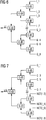
- FIG. 6 shows a possible realization of an I-part of the analog summarizer 2 according to an embodiment of the invention.
- the analog summing unit shown includes a version with pure resistive add-units (I-part) with an insertion loss for 8 channels of 18 dB.
- FIG. 7 shows a possible realization of a Q-part of the analog summarizer 2 according to an embodiment of the invention.
- the analog summing unit shown includes a version with pure resistive couplers with an insertion loss for 8 channels of 18 dB. Important is the 180° phase shift/inversion (NOT) for the even (or odd) channel numbers as we need an upper and a lower side band.
- NOT 180° phase shift/inversion
Landscapes
- Engineering & Computer Science (AREA)
- Computer Networks & Wireless Communication (AREA)
- Signal Processing (AREA)
- Physics & Mathematics (AREA)
- Electromagnetism (AREA)
- Optical Communication System (AREA)
- Digital Transmission Methods That Use Modulated Carrier Waves (AREA)
Abstract
Description
- The invention relates to an optical communication system and to a method of generating a multi-channel signal in an optical network. In particular, the invention relates to a coherent (OLT) transmitter for an Ultra-Dense Wavelength Division Multiplex (UDWDM) network especially for the NSN NGOA (Next Generation Optical Access) system in which a set of densely spaced optical channels is generated from one single laser source.
- Digital signal processing and signal generation allows flexible access networks with variable data rate, modulation format and channel spacing. But a digital signal processing and signal generation based transmitter for optical multi carrier/channel generation needs very fast digital to analog converters for generating the analog signals which are driving the electro optic modulator.
- The first version of our NGOA systems must handle carrier frequencies up to 14 GHz requiring sampling rates of clearly more than 28 Gigasamples per second.
-
FIG. 1 shows a conventional design of OLT TX for coherent UDWDM network (NSN NGOA) based on digital signal processing and ultra fast DACs as interface to analog technology which delivers the analog driving signals. - Analog carrier generation and modulation known in the art as well, but inflexible in terms of data rate, modulation format and channel spacing. Besides that, the development costs of such conventional systems would be extremely high.
- The invention is explained by way of example in more detail below with the aid of the attached drawings.
-
FIG. 1 is a schematic representation a conventional design of OLT TX for coherent UDWDM network (NSN NGOA). -
FIG. 2a shows simulation results, "pseudo-eye" diagrams for the detected signals for a 8 channel OOK system according to an embodiment of the invention. -
FIG, 2b shows simulation results, "pseudo-eye" diagrams for the detected signals for a 8 channel DQPSK system according to an embodiment of the invention. -
FIG. 3 shows a TX concept delivering 8 x 1 Gbit/s channels in which ultra high speed DACs are replaced by ultra high speed digital circuitry according to an embodiment of the invention. -
FIG.4 shows an improved realization of OLT TX with analog summing unit instead of DACs according to an embodiment of the invention. -
FIG.5 shows a realization of OLT TX in which the baseband low-pass filters are employed for pulse shaping according to an embodiment of the invention. -
FIG. 6 shows a possible realization of the analog summing unit according to an embodiment of the invention. -
FIG. 7 shows a possible realization of the analog summing unit according to an embodiment of the invention. - Illustrative embodiments will now be described with reference to the accompanying drawings to disclose the teachings of the present invention. While the present invention is described herein with reference to illustrative embodiments for particular applications, it should be understood that the invention is not limited thereto. Those having ordinary skill in the art and access to the teachings provided herein will recognize additional modifications, applications, and embodiments within the scope thereof and additional fields in which the present invention would be of significant utility.
- The solution provided by an embodiment of the invention suggests a transmitter which utilizes the special spectral properties of digital pulses together with a restriction of the covered frequency range of two succeeding octave bands, e. g. 5 to <15 GHz and low pass filtering in the electrical domain (driving signal) or optical domain (opticl bandpass, WDM filter). Instead of an ultra fast DAC as interface between digital and analog "world" a simple "unweighted" summation of pure digital signals is used. In contrast to that, a DAC uses "weigthed" summation of the respective term, which requires stringent adjustment and timing.
- In case of ON-OFF keying the carriers are generated by pure digital 0-1 sequences and with help of an AND gate or much better a fast analog multiplier the modulation via low pass filtered pure digital signal is done.
- In case of an ideal AND gate as modulator we have overlapping spectra and high channel crosstalk without additional analog filtering.
- The reason that this works is that the spectra are a linear functions and that the Fourier coefficients for a 0-1 sequence contains only the odd terms, see e. g. Bronstein, Taschenbuch der Mathematik, 19. Auflage, 1979, chapter 4.4.1.2 "Tabelle einiger Fourierentwicklungen"
A sequence of 0-1 is discribed by:
- This means, that a 0-1 sequence according to 5 GHz has decreasing Fourier coefficients for 15, 25 ... GHz,
the 0-1 sequence according to 8 GHz has decreasing Fourier coefficients for 24, 40 ... GHz,
the 0-1 sequence according to 11 GHz has decreasing Fourier coefficients for 33, 55 ... GHz,
and the 0-1 sequence according to 14 GHz has decreasing fourier coefficients for 42, 70 ... GHz, - Therefore a frequency plan according to NGOA with e.g. 2
times 4 channels can be realized by pure digital carrier generation. - If the digital carriers are low pass filtered with fg< 3* fcarrier the "two succeeding octave-band limitation" no longer limits the frequency plan - meaning that the 3rd order harmonic has a higher frequency than the carrier with the highest frequency. Only low pass filters are necessary in this case.
- Of course, other carrier frequencies e.g. 2, 5, 8, 11 GHz or 8, 11, 14, 17 GHz or more carrier frequencies / channels are possible according to technical requirements (1GHz is here the channel distance between adjacent channels, if all channels are used).
-
FIG. 2a shows simulation results, "pseudo-eye" diagrams for the detected signals for a 8 channel OOK system according to an embodiment of the invention. -
FIG. 2b shows simulation results, "pseudo-eye" diagrams for the detected signals for a 8 channel DQPSK system according to an embodiment of the invention. - The 90° phase shift between the 2 orthogonal carriers for the DQPSK signal is realized by a time delay between the 0-1 sequences of ½ of the duration of a '1' (or '0').
- The speed of the digital electronics must therefore be able to handle 56 Gb/s (equivalent to 28 GHz) for signals on 14 GHz carriers.
-
FIG. 3 shows a TX concept delivering 10 x 1 Gbit/s channels in which ultra high speed DACs are replaced by ultra high speed digital circuitry and ananalog summarizer 2 according to an embodiment of the invention. Ten received 1 Gb/sdata signals 1G(1) - 1G(10) are fed to aconversion unit 1 and converted into multi-channel signals with different electrical carrier frequencies. First, the received data signals are processed in signal processing units 11 (only one unit is denoted), e.g. framing information and forward error correction parity bits may be added. The completed 'data signals' are then modulated, in the shown embodiment QPSK (quadrature phase shift keying) is used. The modulated base-band signals are then converted in modulated "wavelength division signals" with higher and different carriers corresponding to the channels/signals of a WDM (wavelength division multiplexed) signal. All known conversion methods may be used like using stored conversion tables, technical or mathematical processing. If an above mentioned AND-gate is used as up-conversion unit, the logical 1 of the data signal is combined with the 1, 0-sequence of a carrier with much higher frequency, and the logical data "1" is output ascarrier 1, 0-sequence. - The outputs of all up-conversion units 21 (only one is denoted) are fed to an
analog summarizer 2, band-pass filtered and added. Today, the summarizer comprisespassive summing units 22 which are depicted inFIG. 6 and FIG. 7 . Because QPSK is used, two summing units are necessary for the real components "I" and the imaginary components "Q". The signals corresponding to sums ∑I(t), ∑Q(t) are fed via additionallow pass filters adjustable amplifiers optical IQ modulator 7 outputting an optical WDM signal comprising QPSK signals. -
FIG. 4 shows an improved realization of OLT TX for 8 channels with analog summing unit instead of DACs andanalog modulators 9 according to a further improved embodiment of the invention. The complicated or insufficient functioning up-conversion units are substituted by (preferable) analog multipliers 9 (only one multiplier is denoted). Different carriers, here with frequencies of 5, 8, 11 and 14 GHz and with 90° different phases are fed as modulation signals to themultipliers 9. The band-passes shown inFIG. 3 are substituted by cheaperlow pass filters 8 which are arranged upstream in series with the multipliers. Of course, both signal components I and Q are individually low pass filtered and fed to an multiplier, parallel or serial. - Again, the driving signal for the IQ modulator is an analog sum of filtered up-converted "wavelength diversity signals" all having the about the same weight. The
low pass filters -
FIG. 5 shows a preferred realization of OLT TX shown inFIG. 4 , wherein additional low-pass filters 10 are employed for pulse shaping of the carrier signals, e.g. converting into sinus signals. This embodiment avoids unwanted modulation products. -
FIG. 6 shows a possible realization of an I-part of theanalog summarizer 2 according to an embodiment of the invention. The analog summing unit shown includes a version with pure resistive add-units (I-part) with an insertion loss for 8 channels of 18 dB. -
FIG. 7 shows a possible realization of a Q-part of theanalog summarizer 2 according to an embodiment of the invention. The analog summing unit shown includes a version with pure resistive couplers with an insertion loss for 8 channels of 18 dB. Important is the 180° phase shift/inversion (NOT) for the even (or odd) channel numbers as we need an upper and a lower side band. - The invention bears the following advantages:
- no ultra fast DACs as interface between digital and analog "world".
- ultra high speed DACs are replaced by ultra high speed digital circuitry.
- The present invention is not limited to the details of the above described principles. The scope of the invention is defined by the appended claims and all changes and modifications as fall within the equivalents of the scope of the claims are therefore to be embraced by the invention. Mathematical conversions or equivalent calculations of the signal values based on the inventive method or the use of analogue signals instead of digital values are also incorporated.
-
Reference Signs 1 conversion unit 1G(1) data signal 11 signal processing unit 12 modulator(s) 13 up-conversion unit(s) 2 analog summarizer 21 band- pass 22 add- unit 3, 4 low- pass filter 5, 6 adjustable amplifier 7 optical modulator 8 carrier low- pass filter 9 analog multiplier(s)
Claims (13)
- Multi-channel transmitter for optical networks, comprising- a plurality of parallel modulators (QPSK Mod), each modulating a data signal and outputting a modulated base-band signal (I, Q);- digital frequency conversion units (9; 13) receiving the modulated base-band signals (I, Q) and converting the modulated base-band signals (I, Q) into wavelength division signals (WDS) with higher and different carrier frequencies;- an analog summarizer (7) receiving the wavelength division signals (WDS) and outputting a modulation signal (∑I(t), ∑Q(t)); and
an optical modulator (7) for modulating an optical carrier receiving said modulation signal (∑I(t), ∑Q(t)). - The multi-channel transmitter according to claim 1, comprising
a logical binary gate as digital frequency conversion unit (13) and a band-pass (21) connected downstream in series. - The multi-channel transmitter according to claim 1, comprising
an analog multiplier (9) as digital frequency conversion unit and a low-pass filter (8) connected upstream in series. - The multi-channel transmitter according to one of the preceding claims, wherein
a 0-1 sequence signal is used as carrier for signal conversion. - The multi-channel transmitter according to one of the preceding claims, wherein
the electrical modulators (12) are QPSK modulators and the optical modulator (7) is an optical IQ modulator. - The multi-channel transmitter according to one of the preceding claims, wherein
the electrical carriers have a frequency distance of 3 times a channel distance. - The multi-channel transmitter according claim 6, wherein the highest carrier frequency is less than 3 times the frequency of the lowest electrical carrier frequency.
- A method for generating a multi channel frequency multiplex division signal, comprising the steps of- modulating data signals generating modulated baseband signals (I, Q);- converting modulated base-band signals (I, Q) into wavelength division signals (WDS) with higher and different carrier frequencies (5, 8, 11, 14 GHz);- analog adding the wavelength division signals (WDS) gaining a modulation signal (∑I(t), ∑Q(t)); and- modulating an optical carrier.
- The method according to claim 8, wherein
the modulated base-band signals (I, Q) are frequency converted by multiplying with a 0-1 sequence signal. - The method according to claim 9, wherein
the wavelength division signals have a carrier frequency distance of 3 times a channel distance. - The method according to claim 10, wherein
the highest carrier frequency is less than 3 times the frequency of the lowest electrical carrier frequency. - The method according to claim 8, wherein
the modulated base-band signals (I, Q) are frequency converted by multiplying with a low pass filtered 0-1- sequence carrier signal. - The method according to one of the claim 8 - 12, wherein
the carrier signals and/or baseband signals (I, Q) and/or the modulation signal (∑I(t), ∑Q(t)) are low pass filtered.
Priority Applications (1)
| Application Number | Priority Date | Filing Date | Title |
|---|---|---|---|
| EP12197900.9A EP2611048B1 (en) | 2011-12-30 | 2012-12-18 | Multi-channel transmitter for coherent udwdm networks and method for generating a multi-channel signal |
Applications Claiming Priority (2)
| Application Number | Priority Date | Filing Date | Title |
|---|---|---|---|
| EP11196223 | 2011-12-30 | ||
| EP12197900.9A EP2611048B1 (en) | 2011-12-30 | 2012-12-18 | Multi-channel transmitter for coherent udwdm networks and method for generating a multi-channel signal |
Related Parent Applications (2)
| Application Number | Title | Priority Date | Filing Date |
|---|---|---|---|
| EP11196223.9 Addition | 2011-12-30 | ||
| EP11196223 Addition | 2011-12-30 | 2011-12-30 |
Publications (2)
| Publication Number | Publication Date |
|---|---|
| EP2611048A1 true EP2611048A1 (en) | 2013-07-03 |
| EP2611048B1 EP2611048B1 (en) | 2015-02-11 |
Family
ID=47358386
Family Applications (1)
| Application Number | Title | Priority Date | Filing Date |
|---|---|---|---|
| EP12197900.9A Active EP2611048B1 (en) | 2011-12-30 | 2012-12-18 | Multi-channel transmitter for coherent udwdm networks and method for generating a multi-channel signal |
Country Status (1)
| Country | Link |
|---|---|
| EP (1) | EP2611048B1 (en) |
Citations (3)
| Publication number | Priority date | Publication date | Assignee | Title |
|---|---|---|---|---|
| WO2002017534A1 (en) * | 2000-08-25 | 2002-02-28 | Centerpoint Broadband Technologies, Inc. | A fiber optic terminal system employing subcarrier multiplexing for high capacity optical data transport |
| US6504636B1 (en) * | 1998-06-11 | 2003-01-07 | Kabushiki Kaisha Toshiba | Optical communication system |
| EP1501206A1 (en) * | 2002-04-12 | 2005-01-26 | Telefonica, S.A. | Access method and connection system by means of optical fiber using dwdm/scm hybrid techniques between base stations and remote antennas in a radiocommunication system |
-
2012
- 2012-12-18 EP EP12197900.9A patent/EP2611048B1/en active Active
Patent Citations (3)
| Publication number | Priority date | Publication date | Assignee | Title |
|---|---|---|---|---|
| US6504636B1 (en) * | 1998-06-11 | 2003-01-07 | Kabushiki Kaisha Toshiba | Optical communication system |
| WO2002017534A1 (en) * | 2000-08-25 | 2002-02-28 | Centerpoint Broadband Technologies, Inc. | A fiber optic terminal system employing subcarrier multiplexing for high capacity optical data transport |
| EP1501206A1 (en) * | 2002-04-12 | 2005-01-26 | Telefonica, S.A. | Access method and connection system by means of optical fiber using dwdm/scm hybrid techniques between base stations and remote antennas in a radiocommunication system |
Also Published As
| Publication number | Publication date |
|---|---|
| EP2611048B1 (en) | 2015-02-11 |
Similar Documents
| Publication | Publication Date | Title |
|---|---|---|
| EP1379042B1 (en) | Multiplexer | |
| US9716552B2 (en) | OTDM coherent transceiver | |
| CN101621336B (en) | Difference quadrature phase keying system, method and device | |
| EP2312770B1 (en) | Optical transmission method and apparatus using OFDM | |
| US8818206B2 (en) | Electrical domain suppression of linear crosstalk in optical communication systems | |
| US10469163B2 (en) | Optical channel monitoring using expanded-spectrum pilot tone | |
| CN1491510A (en) | Improvements in Optical Communications | |
| EP1059758A2 (en) | Optical transmitter and optical transmitter control method using variable duty ratio setting and alternate phase inversion for optical clock pulses | |
| JP5585589B2 (en) | Light modulation apparatus and light modulation method | |
| EP3497825B1 (en) | Encoding for optical transmission | |
| Proietti et al. | Elastic optical networking by dynamic optical arbitrary waveform generation and measurement | |
| Geisler et al. | Demonstration of a flexible bandwidth optical transmitter/receiver system scalable to terahertz bandwidths | |
| Du et al. | Flexible all-optical OFDM using WSSs | |
| US10348407B2 (en) | Receiving device and receiving method | |
| EP2611048B1 (en) | Multi-channel transmitter for coherent udwdm networks and method for generating a multi-channel signal | |
| CN103117831A (en) | Upstream channel accessing device of passive optical network system | |
| EP1633061B1 (en) | Method and system for increasing the spectral efficiency of binary coded digital signals | |
| US9425898B2 (en) | Optical transmission system, optical phase modulator, and optical modulation method | |
| Deng et al. | Experimental demonstration and performance evaluation of flexible add/drop operations of DSP-switched ROADMs for cloud access networks | |
| WO2014114329A1 (en) | Optical comb generator | |
| Weng et al. | Spectrally efficient Nyquist-WDM PDM-64QAM signal generation using interleaved DAC with zero-order holding | |
| US20020181064A1 (en) | Method and system for duobinary coding of optical signals | |
| JP4199611B2 (en) | Optical wavelength division multiplexing equipment | |
| Nölle et al. | Techniques to realize flexible optical terabit-per-second transmission systems | |
| Hillerkuss et al. | Low-complexity optical FFT scheme enabling Tbit/s all-optical OFDM communication |
Legal Events
| Date | Code | Title | Description |
|---|---|---|---|
| PUAI | Public reference made under article 153(3) epc to a published international application that has entered the european phase |
Free format text: ORIGINAL CODE: 0009012 |
|
| AK | Designated contracting states |
Kind code of ref document: A1 Designated state(s): AL AT BE BG CH CY CZ DE DK EE ES FI FR GB GR HR HU IE IS IT LI LT LU LV MC MK MT NL NO PL PT RO RS SE SI SK SM TR |
|
| AX | Request for extension of the european patent |
Extension state: BA ME |
|
| RAP1 | Party data changed (applicant data changed or rights of an application transferred) |
Owner name: NOKIA SOLUTIONS AND NETWORKS OY |
|
| RAP1 | Party data changed (applicant data changed or rights of an application transferred) |
Owner name: XIEON NETWORKS S.A.R.L. |
|
| 17P | Request for examination filed |
Effective date: 20140103 |
|
| RBV | Designated contracting states (corrected) |
Designated state(s): AL AT BE BG CH CY CZ DE DK EE ES FI FR GB GR HR HU IE IS IT LI LT LU LV MC MK MT NL NO PL PT RO RS SE SI SK SM TR |
|
| RIC1 | Information provided on ipc code assigned before grant |
Ipc: H04L 27/26 20060101ALI20140131BHEP Ipc: H04B 10/50 20130101AFI20140131BHEP Ipc: H04J 14/02 20060101ALI20140131BHEP |
|
| GRAP | Despatch of communication of intention to grant a patent |
Free format text: ORIGINAL CODE: EPIDOSNIGR1 |
|
| INTG | Intention to grant announced |
Effective date: 20140314 |
|
| R17P | Request for examination filed (corrected) |
Effective date: 20131223 |
|
| RBV | Designated contracting states (corrected) |
Designated state(s): AL AT BE BG CH CY CZ DE DK EE ES FI FR GB GR HR HU IE IS IT LI LT LU LV MC MK MT NL NO PL PT RO RS SE SI SK SM TR |
|
| GRAP | Despatch of communication of intention to grant a patent |
Free format text: ORIGINAL CODE: EPIDOSNIGR1 |
|
| INTG | Intention to grant announced |
Effective date: 20140811 |
|
| GRAS | Grant fee paid |
Free format text: ORIGINAL CODE: EPIDOSNIGR3 |
|
| GRAA | (expected) grant |
Free format text: ORIGINAL CODE: 0009210 |
|
| AK | Designated contracting states |
Kind code of ref document: B1 Designated state(s): AL AT BE BG CH CY CZ DE DK EE ES FI FR GB GR HR HU IE IS IT LI LT LU LV MC MK MT NL NO PL PT RO RS SE SI SK SM TR |
|
| REG | Reference to a national code |
Ref country code: GB Ref legal event code: FG4D |
|
| REG | Reference to a national code |
Ref country code: CH Ref legal event code: EP |
|
| REG | Reference to a national code |
Ref country code: IE Ref legal event code: FG4D |
|
| REG | Reference to a national code |
Ref country code: AT Ref legal event code: REF Ref document number: 710206 Country of ref document: AT Kind code of ref document: T Effective date: 20150315 |
|
| REG | Reference to a national code |
Ref country code: DE Ref legal event code: R096 Ref document number: 602012005224 Country of ref document: DE Effective date: 20150326 |
|
| REG | Reference to a national code |
Ref country code: NL Ref legal event code: VDEP Effective date: 20150211 |
|
| RAP2 | Party data changed (patent owner data changed or rights of a patent transferred) |
Owner name: XIEON NETWORKS S.A R.L. |
|
| REG | Reference to a national code |
Ref country code: AT Ref legal event code: MK05 Ref document number: 710206 Country of ref document: AT Kind code of ref document: T Effective date: 20150211 |
|
| REG | Reference to a national code |
Ref country code: LT Ref legal event code: MG4D |
|
| PG25 | Lapsed in a contracting state [announced via postgrant information from national office to epo] |
Ref country code: FI Free format text: LAPSE BECAUSE OF FAILURE TO SUBMIT A TRANSLATION OF THE DESCRIPTION OR TO PAY THE FEE WITHIN THE PRESCRIBED TIME-LIMIT Effective date: 20150211 Ref country code: NO Free format text: LAPSE BECAUSE OF FAILURE TO SUBMIT A TRANSLATION OF THE DESCRIPTION OR TO PAY THE FEE WITHIN THE PRESCRIBED TIME-LIMIT Effective date: 20150511 Ref country code: ES Free format text: LAPSE BECAUSE OF FAILURE TO SUBMIT A TRANSLATION OF THE DESCRIPTION OR TO PAY THE FEE WITHIN THE PRESCRIBED TIME-LIMIT Effective date: 20150211 Ref country code: HR Free format text: LAPSE BECAUSE OF FAILURE TO SUBMIT A TRANSLATION OF THE DESCRIPTION OR TO PAY THE FEE WITHIN THE PRESCRIBED TIME-LIMIT Effective date: 20150211 Ref country code: LT Free format text: LAPSE BECAUSE OF FAILURE TO SUBMIT A TRANSLATION OF THE DESCRIPTION OR TO PAY THE FEE WITHIN THE PRESCRIBED TIME-LIMIT Effective date: 20150211 Ref country code: SE Free format text: LAPSE BECAUSE OF FAILURE TO SUBMIT A TRANSLATION OF THE DESCRIPTION OR TO PAY THE FEE WITHIN THE PRESCRIBED TIME-LIMIT Effective date: 20150211 |
|
| PG25 | Lapsed in a contracting state [announced via postgrant information from national office to epo] |
Ref country code: RS Free format text: LAPSE BECAUSE OF FAILURE TO SUBMIT A TRANSLATION OF THE DESCRIPTION OR TO PAY THE FEE WITHIN THE PRESCRIBED TIME-LIMIT Effective date: 20150211 Ref country code: NL Free format text: LAPSE BECAUSE OF FAILURE TO SUBMIT A TRANSLATION OF THE DESCRIPTION OR TO PAY THE FEE WITHIN THE PRESCRIBED TIME-LIMIT Effective date: 20150211 Ref country code: IS Free format text: LAPSE BECAUSE OF FAILURE TO SUBMIT A TRANSLATION OF THE DESCRIPTION OR TO PAY THE FEE WITHIN THE PRESCRIBED TIME-LIMIT Effective date: 20150611 Ref country code: GR Free format text: LAPSE BECAUSE OF FAILURE TO SUBMIT A TRANSLATION OF THE DESCRIPTION OR TO PAY THE FEE WITHIN THE PRESCRIBED TIME-LIMIT Effective date: 20150512 Ref country code: LV Free format text: LAPSE BECAUSE OF FAILURE TO SUBMIT A TRANSLATION OF THE DESCRIPTION OR TO PAY THE FEE WITHIN THE PRESCRIBED TIME-LIMIT Effective date: 20150211 Ref country code: AT Free format text: LAPSE BECAUSE OF FAILURE TO SUBMIT A TRANSLATION OF THE DESCRIPTION OR TO PAY THE FEE WITHIN THE PRESCRIBED TIME-LIMIT Effective date: 20150211 |
|
| PG25 | Lapsed in a contracting state [announced via postgrant information from national office to epo] |
Ref country code: DK Free format text: LAPSE BECAUSE OF FAILURE TO SUBMIT A TRANSLATION OF THE DESCRIPTION OR TO PAY THE FEE WITHIN THE PRESCRIBED TIME-LIMIT Effective date: 20150211 Ref country code: CZ Free format text: LAPSE BECAUSE OF FAILURE TO SUBMIT A TRANSLATION OF THE DESCRIPTION OR TO PAY THE FEE WITHIN THE PRESCRIBED TIME-LIMIT Effective date: 20150211 Ref country code: RO Free format text: LAPSE BECAUSE OF FAILURE TO SUBMIT A TRANSLATION OF THE DESCRIPTION OR TO PAY THE FEE WITHIN THE PRESCRIBED TIME-LIMIT Effective date: 20150211 Ref country code: SK Free format text: LAPSE BECAUSE OF FAILURE TO SUBMIT A TRANSLATION OF THE DESCRIPTION OR TO PAY THE FEE WITHIN THE PRESCRIBED TIME-LIMIT Effective date: 20150211 Ref country code: EE Free format text: LAPSE BECAUSE OF FAILURE TO SUBMIT A TRANSLATION OF THE DESCRIPTION OR TO PAY THE FEE WITHIN THE PRESCRIBED TIME-LIMIT Effective date: 20150211 |
|
| REG | Reference to a national code |
Ref country code: DE Ref legal event code: R097 Ref document number: 602012005224 Country of ref document: DE |
|
| PG25 | Lapsed in a contracting state [announced via postgrant information from national office to epo] |
Ref country code: PL Free format text: LAPSE BECAUSE OF FAILURE TO SUBMIT A TRANSLATION OF THE DESCRIPTION OR TO PAY THE FEE WITHIN THE PRESCRIBED TIME-LIMIT Effective date: 20150211 |
|
| PLBE | No opposition filed within time limit |
Free format text: ORIGINAL CODE: 0009261 |
|
| STAA | Information on the status of an ep patent application or granted ep patent |
Free format text: STATUS: NO OPPOSITION FILED WITHIN TIME LIMIT |
|
| PG25 | Lapsed in a contracting state [announced via postgrant information from national office to epo] |
Ref country code: IT Free format text: LAPSE BECAUSE OF FAILURE TO SUBMIT A TRANSLATION OF THE DESCRIPTION OR TO PAY THE FEE WITHIN THE PRESCRIBED TIME-LIMIT Effective date: 20150211 |
|
| 26N | No opposition filed |
Effective date: 20151112 |
|
| PG25 | Lapsed in a contracting state [announced via postgrant information from national office to epo] |
Ref country code: SI Free format text: LAPSE BECAUSE OF FAILURE TO SUBMIT A TRANSLATION OF THE DESCRIPTION OR TO PAY THE FEE WITHIN THE PRESCRIBED TIME-LIMIT Effective date: 20150211 |
|
| PG25 | Lapsed in a contracting state [announced via postgrant information from national office to epo] |
Ref country code: BE Free format text: LAPSE BECAUSE OF FAILURE TO SUBMIT A TRANSLATION OF THE DESCRIPTION OR TO PAY THE FEE WITHIN THE PRESCRIBED TIME-LIMIT Effective date: 20150211 |
|
| PG25 | Lapsed in a contracting state [announced via postgrant information from national office to epo] |
Ref country code: MC Free format text: LAPSE BECAUSE OF FAILURE TO SUBMIT A TRANSLATION OF THE DESCRIPTION OR TO PAY THE FEE WITHIN THE PRESCRIBED TIME-LIMIT Effective date: 20150211 Ref country code: LU Free format text: LAPSE BECAUSE OF FAILURE TO SUBMIT A TRANSLATION OF THE DESCRIPTION OR TO PAY THE FEE WITHIN THE PRESCRIBED TIME-LIMIT Effective date: 20151218 |
|
| REG | Reference to a national code |
Ref country code: CH Ref legal event code: PL |
|
| REG | Reference to a national code |
Ref country code: IE Ref legal event code: MM4A |
|
| REG | Reference to a national code |
Ref country code: FR Ref legal event code: ST Effective date: 20160831 |
|
| PG25 | Lapsed in a contracting state [announced via postgrant information from national office to epo] |
Ref country code: IE Free format text: LAPSE BECAUSE OF NON-PAYMENT OF DUE FEES Effective date: 20151218 Ref country code: CH Free format text: LAPSE BECAUSE OF NON-PAYMENT OF DUE FEES Effective date: 20151231 Ref country code: LI Free format text: LAPSE BECAUSE OF NON-PAYMENT OF DUE FEES Effective date: 20151231 |
|
| PG25 | Lapsed in a contracting state [announced via postgrant information from national office to epo] |
Ref country code: FR Free format text: LAPSE BECAUSE OF NON-PAYMENT OF DUE FEES Effective date: 20151231 |
|
| PG25 | Lapsed in a contracting state [announced via postgrant information from national office to epo] |
Ref country code: BG Free format text: LAPSE BECAUSE OF FAILURE TO SUBMIT A TRANSLATION OF THE DESCRIPTION OR TO PAY THE FEE WITHIN THE PRESCRIBED TIME-LIMIT Effective date: 20150211 Ref country code: HU Free format text: LAPSE BECAUSE OF FAILURE TO SUBMIT A TRANSLATION OF THE DESCRIPTION OR TO PAY THE FEE WITHIN THE PRESCRIBED TIME-LIMIT; INVALID AB INITIO Effective date: 20121218 Ref country code: SM Free format text: LAPSE BECAUSE OF FAILURE TO SUBMIT A TRANSLATION OF THE DESCRIPTION OR TO PAY THE FEE WITHIN THE PRESCRIBED TIME-LIMIT Effective date: 20150211 |
|
| PG25 | Lapsed in a contracting state [announced via postgrant information from national office to epo] |
Ref country code: CY Free format text: LAPSE BECAUSE OF FAILURE TO SUBMIT A TRANSLATION OF THE DESCRIPTION OR TO PAY THE FEE WITHIN THE PRESCRIBED TIME-LIMIT Effective date: 20150211 |
|
| PG25 | Lapsed in a contracting state [announced via postgrant information from national office to epo] |
Ref country code: MT Free format text: LAPSE BECAUSE OF FAILURE TO SUBMIT A TRANSLATION OF THE DESCRIPTION OR TO PAY THE FEE WITHIN THE PRESCRIBED TIME-LIMIT Effective date: 20150211 |
|
| PG25 | Lapsed in a contracting state [announced via postgrant information from national office to epo] |
Ref country code: MK Free format text: LAPSE BECAUSE OF FAILURE TO SUBMIT A TRANSLATION OF THE DESCRIPTION OR TO PAY THE FEE WITHIN THE PRESCRIBED TIME-LIMIT Effective date: 20150211 Ref country code: PT Free format text: LAPSE BECAUSE OF FAILURE TO SUBMIT A TRANSLATION OF THE DESCRIPTION OR TO PAY THE FEE WITHIN THE PRESCRIBED TIME-LIMIT Effective date: 20150211 Ref country code: TR Free format text: LAPSE BECAUSE OF FAILURE TO SUBMIT A TRANSLATION OF THE DESCRIPTION OR TO PAY THE FEE WITHIN THE PRESCRIBED TIME-LIMIT Effective date: 20150211 |
|
| PG25 | Lapsed in a contracting state [announced via postgrant information from national office to epo] |
Ref country code: AL Free format text: LAPSE BECAUSE OF FAILURE TO SUBMIT A TRANSLATION OF THE DESCRIPTION OR TO PAY THE FEE WITHIN THE PRESCRIBED TIME-LIMIT Effective date: 20150211 |
|
| PGFP | Annual fee paid to national office [announced via postgrant information from national office to epo] |
Ref country code: GB Payment date: 20181218 Year of fee payment: 7 |
|
| GBPC | Gb: european patent ceased through non-payment of renewal fee |
Effective date: 20191218 |
|
| PG25 | Lapsed in a contracting state [announced via postgrant information from national office to epo] |
Ref country code: GB Free format text: LAPSE BECAUSE OF NON-PAYMENT OF DUE FEES Effective date: 20191218 |
|
| PGFP | Annual fee paid to national office [announced via postgrant information from national office to epo] |
Ref country code: DE Payment date: 20251104 Year of fee payment: 14 |