EP2608515A2 - Image forming aparatus with power saving mode - Google Patents
Image forming aparatus with power saving mode Download PDFInfo
- Publication number
- EP2608515A2 EP2608515A2 EP12197718.5A EP12197718A EP2608515A2 EP 2608515 A2 EP2608515 A2 EP 2608515A2 EP 12197718 A EP12197718 A EP 12197718A EP 2608515 A2 EP2608515 A2 EP 2608515A2
- Authority
- EP
- European Patent Office
- Prior art keywords
- microcomputer
- image forming
- forming apparatus
- turned
- switching unit
- Prior art date
- Legal status (The legal status is an assumption and is not a legal conclusion. Google has not performed a legal analysis and makes no representation as to the accuracy of the status listed.)
- Granted
Links
Images





Classifications
-
- H—ELECTRICITY
- H04—ELECTRIC COMMUNICATION TECHNIQUE
- H04N—PICTORIAL COMMUNICATION, e.g. TELEVISION
- H04N1/00—Scanning, transmission or reproduction of documents or the like, e.g. facsimile transmission; Details thereof
- H04N1/00885—Power supply means, e.g. arrangements for the control of power supply to the apparatus or components thereof
- H04N1/00888—Control thereof
- H04N1/00896—Control thereof using a low-power mode, e.g. standby
-
- G—PHYSICS
- G06—COMPUTING OR CALCULATING; COUNTING
- G06F—ELECTRIC DIGITAL DATA PROCESSING
- G06F3/00—Input arrangements for transferring data to be processed into a form capable of being handled by the computer; Output arrangements for transferring data from processing unit to output unit, e.g. interface arrangements
- G06F3/12—Digital output to print unit, e.g. line printer, chain printer
- G06F3/1201—Dedicated interfaces to print systems
-
- G—PHYSICS
- G03—PHOTOGRAPHY; CINEMATOGRAPHY; ANALOGOUS TECHNIQUES USING WAVES OTHER THAN OPTICAL WAVES; ELECTROGRAPHY; HOLOGRAPHY
- G03G—ELECTROGRAPHY; ELECTROPHOTOGRAPHY; MAGNETOGRAPHY
- G03G15/00—Apparatus for electrographic processes using a charge pattern
-
- G—PHYSICS
- G06—COMPUTING OR CALCULATING; COUNTING
- G06K—GRAPHICAL DATA READING; PRESENTATION OF DATA; RECORD CARRIERS; HANDLING RECORD CARRIERS
- G06K15/00—Arrangements for producing a permanent visual presentation of the output data, e.g. computer output printers
- G06K15/002—Interacting with the operator
-
- G—PHYSICS
- G06—COMPUTING OR CALCULATING; COUNTING
- G06K—GRAPHICAL DATA READING; PRESENTATION OF DATA; RECORD CARRIERS; HANDLING RECORD CARRIERS
- G06K15/00—Arrangements for producing a permanent visual presentation of the output data, e.g. computer output printers
- G06K15/40—Details not directly involved in printing, e.g. machine management, management of the arrangement as a whole or of its constitutive parts
- G06K15/4055—Managing power consumption, e.g. standby mode
-
- H—ELECTRICITY
- H04—ELECTRIC COMMUNICATION TECHNIQUE
- H04N—PICTORIAL COMMUNICATION, e.g. TELEVISION
- H04N1/00—Scanning, transmission or reproduction of documents or the like, e.g. facsimile transmission; Details thereof
- H04N1/0035—User-machine interface; Control console
-
- H—ELECTRICITY
- H04—ELECTRIC COMMUNICATION TECHNIQUE
- H04N—PICTORIAL COMMUNICATION, e.g. TELEVISION
- H04N1/00—Scanning, transmission or reproduction of documents or the like, e.g. facsimile transmission; Details thereof
- H04N1/0035—User-machine interface; Control console
- H04N1/00496—Constructional details of the interface or console not otherwise provided for, e.g. rotating or tilting means
-
- H—ELECTRICITY
- H04—ELECTRIC COMMUNICATION TECHNIQUE
- H04N—PICTORIAL COMMUNICATION, e.g. TELEVISION
- H04N2201/00—Indexing scheme relating to scanning, transmission or reproduction of documents or the like, and to details thereof
- H04N2201/0077—Types of the still picture apparatus
- H04N2201/0082—Image hardcopy reproducer
-
- H—ELECTRICITY
- H04—ELECTRIC COMMUNICATION TECHNIQUE
- H04N—PICTORIAL COMMUNICATION, e.g. TELEVISION
- H04N2201/00—Indexing scheme relating to scanning, transmission or reproduction of documents or the like, and to details thereof
- H04N2201/0077—Types of the still picture apparatus
- H04N2201/0094—Multifunctional device, i.e. a device capable of all of reading, reproducing, copying, facsimile transception, file transception
Definitions
- Embodiments of the present inventive concept relate to an image forming apparatus which can effectively reduce power consumption.
- An image forming apparatus for example, a multi-function printer (MFP) may be broadly divided into two parts, namely, an operating panel part which accepts a user input, and a main control part which controls operations of the MFP such as actual copying, scanning and printing tasks.
- the user input is received in the operating panel part, and the main control part is requested to perform a task. Thereafter, the operating panel part receives the result of the task and displays the result.
- the operating panel part and the main control part of an image forming apparatus were composed of one CPI and one board, but in order to provide better speed and user experience (UX), the operating panel part has recently been composed of one operating panel microcomputer and one board, and the main control part is composed of one CPU and one board.
- a sleep mode is turned on, and thus power of main components is turned off, thereby effectively reducing power consumption.
- the control panel microcomputer of the control panel part should maintain power-on state even in the sleep mode.
- Exemplary embodiments of the present inventive concept provide an image forming apparatus having an operating panel part to display a screen for input of a command from a user and to receive the command from the user, the image forming apparatus includes a central processing unit (CPU) to control an operation of the image forming apparatus, and an operating panel microcomputer provided in the operating panel part, the microcomputer receiving a reset signal input from the CPU, wherein the CPU changes a voltage level of the reset signal input to the operating panel microcomputer to stop an operation of the operating panel microcomputer in a sleep mode.
- CPU central processing unit
- the operating panel part may include an element to indicate that the image forming apparatus is powered on, and a switching unit to turn on or off to supply an operating voltage to the element, wherein the switching unit is turned off by a switching signal, the switching signal being output when the operation of the operating panel microcomputer is stopped.
- the switching unit may include a pull-down resistor unit connected to a ground terminal, and a PNP-type transistor having a base connected to the pull-down resistor, a collector connected to one side of the element, and an emitter connected to the operating voltage.
- the element is a power light-emitting diode (LED).
- the operating panel part may include a display unit to display the screen for the input of the command from the user, and a switching unit to turn on or off to supply an operating voltage to the display unit and the operating panel microcomputer, wherein the switching unit is turned off by the reset signal, the reset signal being input to the operating panel microcomputer such that the CPU stops the operation of the operating panel microcomputer in the sleep mode.
- the operating panel part may include a display unit to display a screen to receive a command from the user, a first switching unit to turn on or off to supply an operating voltage to the display unit, and a second switching unit to turn on or off to supply the operating voltage to the operating panel microcomputer, wherein the first switching unit and the second switching unit are turned off by the reset signal, the reset signal being input to the operating panel microcomputer such that the CPU stops the operation of the operating panel microcomputer in the sleep mode.
- Exemplary embodiments of the general inventive concept also provide an image forming apparatus having an operating panel part to display a screen for input of a command from a user and receives the command from the user
- the image forming apparatus may include a central processing unit (CPU) to control an operation of the image forming apparatus, an operating panel microcomputer provided in the operating panel part, the microcomputer receiving a reset signal from the CPU, a display unit to display a screen to receive a command from the user, and a first switching unit turned on or off to supply an operating voltage to the display unit and the operating panel microcomputer, wherein the CPU changes a voltage level of the reset signal, the reset signal being input in the operating panel microcomputer to stop an operation of the operating panel microcomputer in a sleep mode, and wherein the first switching unit is turned off by the reset signal of the changed voltage level.
- CPU central processing unit
- the operating panel part may include an element to indicate that the image forming apparatus is powered on, and a second switching unit to turn on or off to supply an operating voltage to the element, wherein the second switching unit is turned off by a switching signal, the switching signal being output when the operation of the operating panel microcomputer is stopped.
- the second switching unit includes a pull-down resistor connected to a ground terminal, and a PNP-type transistor having a base connected to the pull-down resistor, a collector connected to one side of the element, and an emitter connected to the operating voltage.
- the element is a power light-emitting diode (LED).
- power consumption of the image forming apparatus may be effectively reduced by reducing current consumed in an operating panel microcomputer by stopping the operation of the operating panel microcomputer while operating parts to indicate that the image forming apparatus is in a power-on state in the operating panel part in a sleep mode.
- Exemplary embodiments of the general inventive concept also provide a power control circuit to control power supply to an operating panel part of an image forming apparatus, the power control circuit comprising: an input unit to receive an input of various sets of information to execute tasks of the image forming apparatus and to transmit information to an operating panel (OPE) microcomputer of the operating panel part; a first switching unit to be turned on and off by a switching signal of the OPE microcomputer; and a power LED to indicate that power of the image forming apparatus is at a power-on state to distinguish between a sleep mode and a power-off mode, wherein a VCC power is supplied to the power LED when the first switching unit is at a power-on state and the VCC power supply to the power LED is blocked when the first switching unit is at a power-off state.
- OPE operating panel
- the first switching unit is turned on when the OPE microcomputer is not operated.
- the power control circuit further comprises: a second switching unit to be turned on when the voltage level of a reset signal received from a main CPU of the image forming apparatus is high and to be turned off when the voltage level of the reset signal is low; and an LCD to display an operation state of the image forming apparatus, the LCD to be controlled by a control signal of the OPE microcomputer, wherein when the second switching unit is turned on, the VCC is supplied to the OPE microcomputer, the input unit and the LCD, and wherein when the second switching unit is turned off, the VCC being supplied to the OPE microcomputer, the input unit and the LCD is blocked.
- the OPE microcomputer determines whether the operation mode of the image forming apparatus is a normal mode or a sleep mode according to the information input through the input unit.
- the power control circuit further comprises: a second switching unit to be turned on when the voltage level of a reset signal received from a main CPU of the image forming apparatus is high and to be turned off when the voltage level of the reset signal is low; a third switching unit to be turned on when the voltage level of a reset signal received from a main CPU of the image forming apparatus is high and to be turned off when the voltage level of the reset signal is low; and an LCD to display an operation state of the image forming apparatus, the LCD to be controlled by a control signal of the OPE microcomputer, wherein when the second switching unit is turned on, the VCC is supplied to the LCD and when the second switching unit is turned off, the VCC supplied to the LCD is blocked, and wherein when the third switching unit is turned on a branching operating voltage branched from the VCC is supplied to the OPE microcomputer and the input unit, and if the third switching unit is turned off, the branching operating voltage branched from the VCC and being supplied to the OPE microcomputer and th input unit is
- FIG. 1 is an example of an image forming apparatus according to the present inventive concept, and illustrates a multi-function printer having copying, scanning and printing functions.
- an image forming apparatus includes a main body 10, a scanning unit 20, an auto document feeder (ADF) 30, a paper feeding cassette 40, and an operating panel 100.
- ADF auto document feeder
- Various components for image formation such as a paper feeding unit, a laser scanning unit, a developing unit, a transfer unit, a fusing unit, a paper exhaust unit, and a sensor unit, etc. are installed in the main body 10.
- the scanning unit 20 is disposed on the upper portion, and scans a document.
- the scanning unit 20 copies or scans a document according to a copy command or a scan command.
- the auto document feeder (ADF) 30 feeds papers by automatically releasing each sheet from accumulated sheets of paper.
- the paper feeding cassette 40 is disposed on the lower portion of the main body 10, and accepts multiple sheets of paper.
- the operating panel 50 displays a screen so that the user may select a desired task and give a command to perform the task, and receives a task command such as printing, copying, scanning, etc. from the user.
- the operating panel 50 displays a user interface screen, and has a touch panel function in which buttons formed within the user interface screen are operated by a user's finger, etc.
- the user may operate a button corresponding to a function such as printing, copying, scanning, etc., which is displayed in the user interface screen, to select a desired task.
- FIG. 2 is a diagram illustrating a relation between an operating panel part and a main control part of an image forming apparatus according to an exemplary embodiment of the present inventive concept.
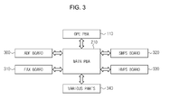
- FIG. 3 is a block diagram illustrating a relation between each printed circuit board assembly (PBA), which constitutes the operation panel part and the main control part of the image forming apparatus, and other boards.
- PBA printed circuit board assembly
- an image forming apparatus includes an operating panel part 100 and a main control part 200.
- the operating panel part 100 displays a screen to accept a user's selection of a task, and receives an input of a task command from the user.
- the main control part 200 controls actual operations of an image forming apparatus such as printing, scanning and printing, and other functions known to those skilled in the art to be performed by an image forming apparatus.
- the operating panel part 100 is configured to be booted earlier than the main control part 200 so that the user may promptly input information.
- the operating panel part 100 and the main control part 200 include a printed circuit board assembly (PBA) composed of one CPU and one board.
- PBA printed circuit board assembly
- the operating panel part 100 includes an operating panel printed circuit board assembly (hereinafter, referred to as “operating panel equipment (OPE) PBA”) 100
- the main control part 200 includes a main printed circuit board assembly (hereinafter, referred to as "main PBA”) 210.
- OPE operating panel equipment
- main PBA main printed circuit board assembly
- the OPE PBA 110 and the main PBA 210 are connected to each other so that communications therebetween are performed.
- Various parts 340 such as an ADF board 300, a fax board 310, a switching mode power supply (SMPS) board 320, a high voltage power supply (HVPS) board 330, and various motors, sensors, fans, etc. are connected to the main PBA 210 to which the OPE PBA 110 is connected so that mutual communication is possible.
- SMPS switching mode power supply
- HPV high voltage power supply
- the ADF board 300 automatically supplies a document when copying or scanning the document.
- the fax board 310 communicates with another MFP or fax device.
- the SMPS board 320 supplies +5V and +24V to the main PBA 201 and other boards from 11 OV/220V power voltage input.
- the HVPS board 330 supplies high voltage to various devices, which require high voltage in the image forming apparatus, such as a photosensitive medium, a charging unit, a developing unit, a transfer unit, etc.
- the main PBA 210 examines the state of all boards 300, 310, 320 and 330 and various parts 340, which are connected to the main PBA 210 except the OPE PBA 110, to complete booting when operation of all the boards and parts is prepared.
- FIG. 4 is a diagram illustrating power supply and signal transmission of a main PBA and an OPE PBA of an image forming apparatus according to an exemplary embodiment of the present inventive concept.
- the main PBA 210 controls actual operations of an image forming apparatus.
- the main PBA 210 includes a CPU 211 and a power supply unit 212.
- the CPU 211 controls overall operations of the image forming apparatus.
- the power supply unit 212 supplies a preset voltage to the OPE PBA 110 according to a control signal of the CPU 211.
- the power supply unit 212 outputs, for example, 24V or 5V.
- the power supply unit 212 is connected with an OPE microcomputer 111, an input unit 112, a first switching unit 113 and a liquid crystal display (LCD), which is a display unit, of the OPE PBA 110 through a power line (PL), and supplies preset voltage to each component.
- OPE microcomputer 111 an input unit 112
- first switching unit 113 a liquid crystal display
- LCD liquid crystal display
- PL power line
- the OPE PBA 110 communicates with the main PBA 210 by exchanging information with the main PBA 210. Further, the OPE PBA 110 includes a key which allows setting and change, etc. of various operation modes of the image forming apparatus, and transmits various key data, which is generated by the user in the image forming apparatus, to the main PBA 210.
- the OPE PBA 110 includes an OPE microcomputer 111, an input unit 112, a first switching unit 113, a power LED 114 and an LCD 115.
- the input unit 112 receives an input of various sets of information to execute a task such as setting and change, etc. of various operation modes from the user.
- the input unit 112 transmits information, which is input by the user, to the OPE microcomputer 111.
- the first switching unit 113 is turned on or off by a switching signal of the OPE microcomputer 111.
- the power LED 114 is a part indicating that the power of the image forming apparatus is at a power-on state so that the user may distinguish the sleep mode from the power-off mode, and is connected with the first switching unit 113 through the power line (PL).
- VCC power is supplied to the power LED 114 when the first switching unit 113 is at the power-on state. Further, VCC power supply to the power LED 114 is blocked when the first switching unit 113 is at the power-off state.
- the LCD 115 is a device to display the operation state of the image forming apparatus.
- the LCD 115 is controlled by a control signal of the OPE microcomputer 111.
- the OPE microcomputer 111 determines whether the operation mode of the image forming apparatus is a normal mode or a sleep mode according to information input through the input unit 112.
- the OPE microcomputer 111 transmits the determined operation mode information of the image forming apparatus to the CPU 211 of the main PBA 210. Further, the OPE microcomputer 111 may determine that the operation mode is a normal mode if time counted by a timer is less than a preset time, and the operation mode is a sleep mode if time counted by the timer is greater than a preset time.
- the CPU 211 controls whether to operate the OPE microcomputer 111 by changing the voltage level of a reset signal, which is output to the OPE microcomputer 111, according to whether the operation mode of the image forming apparatus is a normal mode or a sleep mode.
- the OPE microcomputer 111 is initialized to the voltage level of this reset signal, or performs normal operation.
- the CPU 211 If the operation mode of the image forming apparatus is a normal mode, the CPU 211 outputs a reset signal of a high level in the OPE microcomputer 111.
- the OPE microcomputer 111 becomes operable by this reset signal of a high level.
- the CPU 211 outputs the reset signal having a low level in the OPE microcomputer 111.
- the OPE microcomputer 111 is turned off by this reset signal of the low level, thereby becoming inoperable.
- the state of the ports of the OPE microcomputer 111 become a high impedance state by a reset signal of this low level, thereby falling into an inoperable state.
- the input unit 112, the first switching unit 113 and the LCD 115, which are connected to these ports cannot be controlled.
- the OPE microcomputer 111 rarely consumes electric current, and thus power consumption of the image forming apparatus may be effectively reduced.
- the first switching unit 113 is configured so that the first switching unit 113 may be turned on.
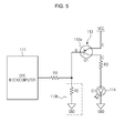
- FIG. 5 is a drawing illustrating operating a power LED when the OPE microcomputer 111 of FIG. 4 is not operated, and describes a principle of turning on the power LED when the OPE microcomputer is not operated.
- the first switching unit 113 includes a PNP-type transistor (Q1) 113a and a pull-down resistor unit 113b.
- the PNP type transistor (Q1) is a combination of semiconductors in which the n-type region is placed between two p-type regions which have a low impurity concentration and are narrow, and includes a base (B), which is a central region, an emitter (E), which is a forward region located outside from this base (B), and a collector (C), which is a backward region.
- the base C of the PNP-type transistor (Q1) 113a is connected via a resistor R1 and a port which outputs a switching signal to switch the first switching unit 113. Further, the emitter E is connected to the operating voltage VCC, and the collector C is connected to the ground terminal (GND) via the power LED 114 and the resistor R3 connected in series.
- the pull-down resistor unit 113b is connected to the ground terminal (GND) and the base (C) of the PNP-type transistor (Q1) 113a, and includes a resistor R1 connected to a port, which outputs a switching signal in the OPE microcomputer 111, and a pull-down resistor R2 connected in parallel.
- the OPE microcomputer 111 When the OPE microcomputer 111 is not operated (a reset signal is at a low level) by using the pull-down resistor R2, the power LED is turned on by turning on the PNP type transistor Q1. That is, the user may recognize the sleep mode.
- the OPE microcomputer 111 may be configured to turn on an error LED instead of turning on the power LED 114 when entering the sleep mode.
- the CPU 211 lowers the voltage level of a reset signal, which is output to the OPE microcomputer 111, to a low level.
- the OPE microcomputer 111 may reduce the power consumed in the OPE microcomputer 111 as the state of ports become a high impedance state by a reset signal of the low level and the operation stops. At this time, even if the state of the ports of the OPE microcomputer 111 become a high impedance state, the pull-down resistor unit 113b is applied to the base B of the PNP type transistor (Q1) 113a so that the power LED 114 may be turned on.
- FIG. 6 is a drawing illustrating power supply and signal transmission of a main PBA and an OPE PBA in an image forming apparatus according to another exemplary embodiment of the present inventive concept.
- the OPE PBA 110 includes an OPE microcomputer 111, an input unit 112, a first switching unit 113, a power LED 114, an LCD 115, and a second switching unit 116.
- the input unit 112 receives an input of various sets of information to execute a task such as setting and change, etc. of various operation modes from a user.
- the input unit 112 transmits information, which is input from the user, to the OPE microcomputer 111.
- the first switching unit 113 is turned on or off by the switching signal of the OPE microcomputer 111.
- the power LED 114 is a part showing that the power of the image forming apparatus is at a power-on state so that the user may distinguish the sleep mode from the power-off mode, and is connected with the first switching unit 113 through the power line (PL).
- VCC power is supplied to the power LED 114 when the first switching unit 113 is at the power-on state. Further, VCC power supply to the power LED 114 is blocked when the first switching unit 113 is at the power-off state.
- the LCD 115 is a device for displaying the operation state of the image forming apparatus.
- the LCD 115 is controlled by a control signal of the OPE microcomputer 111.
- the second switching unit 116 is turned on in the case in which the voltage level of a reset signal, which is output from the CPU 211 to the OPE microcomputer 111, is high, and is turned off in the case in which the voltage level of the reset signal is low.
- operating voltage VCC is supplied to the OPE microcomputer 111, the input unit 112 and the LCD 115. Further, if the second switching unit 116 is turned off, the operating voltage VCC, which is supplied to the OPE microcomputer 111, the input unit 112 and the LCD 115, is blocked.
- the CPU 211 controls whether to operate the OPE microcomputer 111 by changing the voltage level of a reset signal, which is output to the OPE microcomputer 111 according to whether the operation mode of the image forming apparatus is a normal mode or a sleep mode.
- the CPU 211 If the operation mode of the image forming apparatus is a normal mode, the CPU 211 outputs a reset signal of a high level in the OPE microcomputer 111. The state of the OPE microcomputer 111 becomes operable state and the second switching unit 116 is turned on by this reset signal of a high level.
- the CPU 211 outputs the reset signal of a low level in the OPE microcomputer 111.
- the state of the OPE microcomputer 111 becomes inoperable and the second switching unit 116 is turned off by this reset signal of the low level.
- branch operating voltage (VCC_SLP) which is supplied to the OPE microcomputer 111, the input unit 112 and the LCD 115, is blocked.
- parts e.g., a power LED or an inverter
- parts which should be turned on in a sleep mode
- parts e.g., an OPE microcomputer, an input unit and an LCD
- branch operating voltage after the second switching unit 116 are designed to use branch operating voltage after the second switching unit 116.
- the branch operating voltage which is supplied to the OPE microcomputer 111, the input unit 112 and the LCD 115, may be blocked, and thus the power consumption, which is used in the OPE microcomputer 111, the input unit 112 and the LCD 115, may be saved.
- FIG. 6 illustrates a method of reducing power consumption using a voltage level of a reset signal which is output from the CPU 211 to the OPE microcomputer 111 as in FIG. 5 .
- the reset signal is changed to a low level, and the second switching unit 116 is turned on or off by this signal depending on the mode.
- VCC_SLP branch operating voltage
- the OPE microcomputer 111 and the LCD 115, etc. which use this voltage, are not operated, and thus the power consumption may be effectively reduced.
- the power LED 114 is turned on using the pull-down resistor R2 as in FIG. 5 , and when an error occurs, the voltage level of the reset signal is maintained at a high level so that the OPE microcomputer 111 may control the LED.
- FIG. 7 is a drawing illustrating power supply and signal transmission of a main PBA and an OPE PBA in an image forming apparatus according to yet another exemplary embodiment of the present inventive concept.
- the OPE PBA 110 includes a second switching unit 116 and a third switching unit 117.
- the second switching unit 116 is turned on in the case in which the voltage level of the reset signal, which is output from the CPU 211 to the OPE microcomputer 111, is high, and is turned off in the case in which the voltage level of the reset signal is low.
- the operating voltage VCC1 is supplied to the LCD 115. Further, if the second switching unit 116 is turned off, the operating voltage VCC1, which is supplied to the LCD 115, is blocked.
- the third switching unit 117 is turned on in the case in which the voltage level of the reset signal, which is output from the CPU 211 to the OPE microcomputer 111, is high, and is turned off in the case in which the voltage level of the reset signal is low.
- the branch operating voltage (VCC2_SLP) is supplied to the OPE microcomputer 111 and the input unit 112. Further, if the third switching unit 117 is turned off, the branch operating voltage (VCC_SLP), which is supplied to the OPE microcomputer 111 and the input unit 112, is blocked.
- the CPU 211 controls operation of the OPE microcomputer 111 by changing the voltage level of the reset signal which is output to the OPE microcomputer 111 according to whether the operation mode of the image forming apparatus is a normal mode or a sleep mode.
- the CPU 211 If the operation mode of the image forming apparatus is a normal mode, the CPU 211 outputs a reset signal of a high level to the OPE microcomputer 111. By this reset signal of a high level, the OPE microcomputer 111 becomes operable, and the second switching unit 116 and the third switching unit 117 are turned on.
- the CPU 211 outputs a reset signal of a low level to the OPE microcomputer 111.
- the reset signal of a low level the operation of the OPE microcomputer 111 is disabled, and the second switching unit 116 and the third switching unit 117 are turned off.
- the operating voltage VCC1 which is supplied to the LCD 115
- the branch operating voltage VCC2_SLP which is supplied to the input unit 112 and the OPE microcomputer 111, is blocked.
- power consumption is reduced using multiple switching units 116 and 117 which are turned on or off by a voltage level of a reset signal which is output from the CPU 211 to the OPE microcomputer 111 at a sleep mode.
- FIG. 7 is a use example when there are multiple VCC power sources in FIG. 6 . That is, in the OPE PBA 110 which uses multiple power sources, a reset signal is changed to a low level at a sleep mode as in FIG. 6 , and as the multiple switching units 116 and 117 are turned off by this signal, the OPE microcomputer 111, the input unit 112, and the LCD 115 are not operated, thereby reducing power consumption.
- the power LED 114 is turned on using the pull-down resistor R2 as in FIG. 5 , and when an error occurs, the reset signal is maintained at a high level so that the OPE microcomputer 111 may control the LED 114.
Landscapes
- Engineering & Computer Science (AREA)
- General Engineering & Computer Science (AREA)
- Theoretical Computer Science (AREA)
- Physics & Mathematics (AREA)
- General Physics & Mathematics (AREA)
- Multimedia (AREA)
- Signal Processing (AREA)
- Human Computer Interaction (AREA)
- Control Or Security For Electrophotography (AREA)
- Accessory Devices And Overall Control Thereof (AREA)
- Facsimiles In General (AREA)
Abstract
Description
- Embodiments of the present inventive concept relate to an image forming apparatus which can effectively reduce power consumption.
- An image forming apparatus, for example, a multi-function printer (MFP) may be broadly divided into two parts, namely, an operating panel part which accepts a user input, and a main control part which controls operations of the MFP such as actual copying, scanning and printing tasks. The user input is received in the operating panel part, and the main control part is requested to perform a task. Thereafter, the operating panel part receives the result of the task and displays the result.
- In the past, the operating panel part and the main control part of an image forming apparatus were composed of one CPI and one board, but in order to provide better speed and user experience (UX), the operating panel part has recently been composed of one operating panel microcomputer and one board, and the main control part is composed of one CPU and one board.
- Recently, as concern for the environment rapidly increases, many products support a sleep mode, which may be compared to a normal mode, in which unnecessary power consumption may be reduced when the user does not use the product.
- According to the conventional art, when the user does not use a multi-function printer, a sleep mode is turned on, and thus power of main components is turned off, thereby effectively reducing power consumption.
- However, at the sleep mode, in order to continually operate parts for allowing the consumer to distinguish the sleep mode from the power-off mode, such as a power LED, etc. which show that the product is in a power-on state, the control panel microcomputer of the control panel part should maintain power-on state even in the sleep mode.
- As such, even in the sleep mode, power for maintaining the power-on state of the control panel microcomputer is continually consumed.
- It is an aspect of the present inventive concept to provide an image forming apparatus that allows a power voltage to be supplied to parts to allow a consumer to distinguish a sleep mode from a power-off mode while stopping an operation of an OPE microcomputer of an operating panel part in a sleep mode so as to reduce power consumption of the image forming apparatus in the sleep mode.
- Additional features and utilities of the present general inventive concept will be set forth in part in the description which follows and, in part, will be obvious from the description, or may be learned by practice of the general inventive concept.
- Exemplary embodiments of the present inventive concept provide an image forming apparatus having an operating panel part to display a screen for input of a command from a user and to receive the command from the user, the image forming apparatus includes a central processing unit (CPU) to control an operation of the image forming apparatus, and an operating panel microcomputer provided in the operating panel part, the microcomputer receiving a reset signal input from the CPU, wherein the CPU changes a voltage level of the reset signal input to the operating panel microcomputer to stop an operation of the operating panel microcomputer in a sleep mode.
- The operating panel part may include an element to indicate that the image forming apparatus is powered on, and a switching unit to turn on or off to supply an operating voltage to the element, wherein the switching unit is turned off by a switching signal, the switching signal being output when the operation of the operating panel microcomputer is stopped.
- The switching unit may include a pull-down resistor unit connected to a ground terminal, and a PNP-type transistor having a base connected to the pull-down resistor, a collector connected to one side of the element, and an emitter connected to the operating voltage.
- The element is a power light-emitting diode (LED).
- The operating panel part may include a display unit to display the screen for the input of the command from the user, and a switching unit to turn on or off to supply an operating voltage to the display unit and the operating panel microcomputer, wherein the switching unit is turned off by the reset signal, the reset signal being input to the operating panel microcomputer such that the CPU stops the operation of the operating panel microcomputer in the sleep mode.
- The operating panel part may include a display unit to display a screen to receive a command from the user, a first switching unit to turn on or off to supply an operating voltage to the display unit, and a second switching unit to turn on or off to supply the operating voltage to the operating panel microcomputer, wherein the first switching unit and the second switching unit are turned off by the reset signal, the reset signal being input to the operating panel microcomputer such that the CPU stops the operation of the operating panel microcomputer in the sleep mode.
- Exemplary embodiments of the general inventive concept also provide an image forming apparatus having an operating panel part to display a screen for input of a command from a user and receives the command from the user, the image forming apparatus may include a central processing unit (CPU) to control an operation of the image forming apparatus, an operating panel microcomputer provided in the operating panel part, the microcomputer receiving a reset signal from the CPU, a display unit to display a screen to receive a command from the user, and a first switching unit turned on or off to supply an operating voltage to the display unit and the operating panel microcomputer, wherein the CPU changes a voltage level of the reset signal, the reset signal being input in the operating panel microcomputer to stop an operation of the operating panel microcomputer in a sleep mode, and wherein the first switching unit is turned off by the reset signal of the changed voltage level.
- The operating panel part may include an element to indicate that the image forming apparatus is powered on, and a second switching unit to turn on or off to supply an operating voltage to the element, wherein the second switching unit is turned off by a switching signal, the switching signal being output when the operation of the operating panel microcomputer is stopped.
- The second switching unit includes a pull-down resistor connected to a ground terminal, and a PNP-type transistor having a base connected to the pull-down resistor, a collector connected to one side of the element, and an emitter connected to the operating voltage.
- The element is a power light-emitting diode (LED).
- According to the inventive concept, power consumption of the image forming apparatus may be effectively reduced by reducing current consumed in an operating panel microcomputer by stopping the operation of the operating panel microcomputer while operating parts to indicate that the image forming apparatus is in a power-on state in the operating panel part in a sleep mode.
- Exemplary embodiments of the general inventive concept also provide a power control circuit to control power supply to an operating panel part of an image forming apparatus, the power control circuit comprising: an input unit to receive an input of various sets of information to execute tasks of the image forming apparatus and to transmit information to an operating panel (OPE) microcomputer of the operating panel part; a first switching unit to be turned on and off by a switching signal of the OPE microcomputer; and a power LED to indicate that power of the image forming apparatus is at a power-on state to distinguish between a sleep mode and a power-off mode, wherein a VCC power is supplied to the power LED when the first switching unit is at a power-on state and the VCC power supply to the power LED is blocked when the first switching unit is at a power-off state.
- In an exemplary embodiment, the first switching unit is turned on when the OPE microcomputer is not operated.
- In an exemplary embodiment, the power control circuit further comprises: a second switching unit to be turned on when the voltage level of a reset signal received from a main CPU of the image forming apparatus is high and to be turned off when the voltage level of the reset signal is low; and an LCD to display an operation state of the image forming apparatus, the LCD to be controlled by a control signal of the OPE microcomputer, wherein when the second switching unit is turned on, the VCC is supplied to the OPE microcomputer, the input unit and the LCD, and wherein when the second switching unit is turned off, the VCC being supplied to the OPE microcomputer, the input unit and the LCD is blocked.
- In an exemplary embodiment, the OPE microcomputer determines whether the operation mode of the image forming apparatus is a normal mode or a sleep mode according to the information input through the input unit.
- In another exemplary embodiment, the power control circuit further comprises: a second switching unit to be turned on when the voltage level of a reset signal received from a main CPU of the image forming apparatus is high and to be turned off when the voltage level of the reset signal is low; a third switching unit to be turned on when the voltage level of a reset signal received from a main CPU of the image forming apparatus is high and to be turned off when the voltage level of the reset signal is low; and an LCD to display an operation state of the image forming apparatus, the LCD to be controlled by a control signal of the OPE microcomputer, wherein when the second switching unit is turned on, the VCC is supplied to the LCD and when the second switching unit is turned off, the VCC supplied to the LCD is blocked, and wherein when the third switching unit is turned on a branching operating voltage branched from the VCC is supplied to the OPE microcomputer and the input unit, and if the third switching unit is turned off, the branching operating voltage branched from the VCC and being supplied to the OPE microcomputer and th input unit is blocked.
- These and/or other features and utilities of the present general inventive concept will become apparent and more readily appreciated from the following description of the embodiments, taken in conjunction with the accompanying drawings of which:
-
FIG. 1 is an oblique diagram illustrating an image forming apparatus according to an exemplary embodiment of the present inventive concept; -
FIG. 2 is a diagram illustrating a relation between an operating panel part and a main control part of an image forming apparatus according to an exemplary embodiment of the present inventive concept; -
FIG. 3 is a block diagram illustrating a relation between each printed circuit board assembly (PBA), which constitutes the operation panel part and the main control part of the image forming apparatus, and other boards. -
FIG. 4 is a diagram illustrating power supply and signal transmission of a main PBA and an OPE PBA of an image forming apparatus according to an exemplary embodiment of the present inventive concept. -
FIG. 5 is a drawing illustrating operating a power LED when the OPE microcomputer ofFIG. 4 is not operated. -
FIG. 6 is a drawing illustrating power supply and signal transmission of a main PBA and an OPE PBA in an image forming apparatus according to another exemplary embodiment of the present inventive concept. -
FIG. 7 is a drawing illustrating power supply and signal transmission of a main PBA and an OPE PBA in an image forming apparatus according to yet another exemplary embodiment of the present inventive concept. - Reference will now be made in detail to the embodiments of the present general inventive concept, examples of which are illustrated in the accompanying drawings, wherein like reference numerals refer to the like elements throughout. The embodiments are described below in order to explain the present general inventive concept while referring to the figures.
-
FIG. 1 is an example of an image forming apparatus according to the present inventive concept, and illustrates a multi-function printer having copying, scanning and printing functions. - As illustrated in
FIG. 1 , an image forming apparatus includes amain body 10, ascanning unit 20, an auto document feeder (ADF) 30, apaper feeding cassette 40, and anoperating panel 100. - Various components for image formation such as a paper feeding unit, a laser scanning unit, a developing unit, a transfer unit, a fusing unit, a paper exhaust unit, and a sensor unit, etc. are installed in the
main body 10. - The
scanning unit 20 is disposed on the upper portion, and scans a document. Thescanning unit 20 copies or scans a document according to a copy command or a scan command. - The auto document feeder (ADF) 30 feeds papers by automatically releasing each sheet from accumulated sheets of paper.
- The
paper feeding cassette 40 is disposed on the lower portion of themain body 10, and accepts multiple sheets of paper. - The
operating panel 50, as an interface with a user, displays a screen so that the user may select a desired task and give a command to perform the task, and receives a task command such as printing, copying, scanning, etc. from the user. - The
operating panel 50 displays a user interface screen, and has a touch panel function in which buttons formed within the user interface screen are operated by a user's finger, etc. The user may operate a button corresponding to a function such as printing, copying, scanning, etc., which is displayed in the user interface screen, to select a desired task. - Hence, if the user inputs a copying, scanning or printing command through the
operating panel 100, a document, which is placed on the plate of thescanning unit 20, is copied or scanned, or to-be-printed data is printed on sheets stored in thepaper feeding cassette 40. -
FIG. 2 is a diagram illustrating a relation between an operating panel part and a main control part of an image forming apparatus according to an exemplary embodiment of the present inventive concept.FIG. 3 is a block diagram illustrating a relation between each printed circuit board assembly (PBA), which constitutes the operation panel part and the main control part of the image forming apparatus, and other boards. - As illustrated in
FIG. 2 , an image forming apparatus includes anoperating panel part 100 and amain control part 200. - The
operating panel part 100 displays a screen to accept a user's selection of a task, and receives an input of a task command from the user. - The
main control part 200 controls actual operations of an image forming apparatus such as printing, scanning and printing, and other functions known to those skilled in the art to be performed by an image forming apparatus. - If the image forming apparatus is turned on, the
operating panel part 100 is configured to be booted earlier than themain control part 200 so that the user may promptly input information. - The
operating panel part 100 and themain control part 200 include a printed circuit board assembly (PBA) composed of one CPU and one board. - As illustrated in
FIG. 3 , theoperating panel part 100 includes an operating panel printed circuit board assembly (hereinafter, referred to as "operating panel equipment (OPE) PBA") 100, and themain control part 200 includes a main printed circuit board assembly (hereinafter, referred to as "main PBA") 210. - The OPE PBA 110 and the main PBA 210 are connected to each other so that communications therebetween are performed.
-
Various parts 340 such as anADF board 300, afax board 310, a switching mode power supply (SMPS)board 320, a high voltage power supply (HVPS) board 330, and various motors, sensors, fans, etc. are connected to the main PBA 210 to which the OPE PBA 110 is connected so that mutual communication is possible. - The
ADF board 300 automatically supplies a document when copying or scanning the document. - The
fax board 310 communicates with another MFP or fax device. - The
SMPS board 320 supplies +5V and +24V to the main PBA 201 and other boards from 11 OV/220V power voltage input. - The HVPS board 330 supplies high voltage to various devices, which require high voltage in the image forming apparatus, such as a photosensitive medium, a charging unit, a developing unit, a transfer unit, etc.
- The
main PBA 210 examines the state of allboards various parts 340, which are connected to themain PBA 210 except theOPE PBA 110, to complete booting when operation of all the boards and parts is prepared. -
FIG. 4 is a diagram illustrating power supply and signal transmission of a main PBA and an OPE PBA of an image forming apparatus according to an exemplary embodiment of the present inventive concept. - As illustrated in
FIG. 4 , themain PBA 210 controls actual operations of an image forming apparatus. - The
main PBA 210 includes aCPU 211 and apower supply unit 212. - The
CPU 211 controls overall operations of the image forming apparatus. - The
power supply unit 212 supplies a preset voltage to theOPE PBA 110 according to a control signal of theCPU 211. - The
power supply unit 212 outputs, for example, 24V or 5V. - The
power supply unit 212 is connected with anOPE microcomputer 111, aninput unit 112, afirst switching unit 113 and a liquid crystal display (LCD), which is a display unit, of theOPE PBA 110 through a power line (PL), and supplies preset voltage to each component. - The
OPE PBA 110 communicates with themain PBA 210 by exchanging information with themain PBA 210. Further, theOPE PBA 110 includes a key which allows setting and change, etc. of various operation modes of the image forming apparatus, and transmits various key data, which is generated by the user in the image forming apparatus, to themain PBA 210. - The
OPE PBA 110 includes anOPE microcomputer 111, aninput unit 112, afirst switching unit 113, apower LED 114 and anLCD 115. - The
input unit 112 receives an input of various sets of information to execute a task such as setting and change, etc. of various operation modes from the user. Theinput unit 112 transmits information, which is input by the user, to theOPE microcomputer 111. - The
first switching unit 113 is turned on or off by a switching signal of theOPE microcomputer 111. - The
power LED 114 is a part indicating that the power of the image forming apparatus is at a power-on state so that the user may distinguish the sleep mode from the power-off mode, and is connected with thefirst switching unit 113 through the power line (PL). - VCC power is supplied to the
power LED 114 when thefirst switching unit 113 is at the power-on state. Further, VCC power supply to thepower LED 114 is blocked when thefirst switching unit 113 is at the power-off state. - The
LCD 115 is a device to display the operation state of the image forming apparatus. TheLCD 115 is controlled by a control signal of theOPE microcomputer 111. - The
OPE microcomputer 111 determines whether the operation mode of the image forming apparatus is a normal mode or a sleep mode according to information input through theinput unit 112. TheOPE microcomputer 111 transmits the determined operation mode information of the image forming apparatus to theCPU 211 of themain PBA 210. Further, theOPE microcomputer 111 may determine that the operation mode is a normal mode if time counted by a timer is less than a preset time, and the operation mode is a sleep mode if time counted by the timer is greater than a preset time. - The
CPU 211 controls whether to operate theOPE microcomputer 111 by changing the voltage level of a reset signal, which is output to theOPE microcomputer 111, according to whether the operation mode of the image forming apparatus is a normal mode or a sleep mode. TheOPE microcomputer 111 is initialized to the voltage level of this reset signal, or performs normal operation. - If the operation mode of the image forming apparatus is a normal mode, the
CPU 211 outputs a reset signal of a high level in theOPE microcomputer 111. TheOPE microcomputer 111 becomes operable by this reset signal of a high level. - Further, if the operation mode of the image forming apparatus is a sleep mode, the
CPU 211 outputs the reset signal having a low level in theOPE microcomputer 111. TheOPE microcomputer 111 is turned off by this reset signal of the low level, thereby becoming inoperable. - That is, the state of the ports of the
OPE microcomputer 111 become a high impedance state by a reset signal of this low level, thereby falling into an inoperable state. As such, theinput unit 112, thefirst switching unit 113 and theLCD 115, which are connected to these ports, cannot be controlled. Hence, theOPE microcomputer 111 rarely consumes electric current, and thus power consumption of the image forming apparatus may be effectively reduced. - As stated above, since the
power LED 114 needs to maintain the operation state even if theOPE microcomputer 111 is turned off, in the case in which the port, which outputs a switching signal of theOPE microcomputer 111, is at a high impedance state, thefirst switching unit 113 is configured so that thefirst switching unit 113 may be turned on. -
FIG. 5 is a drawing illustrating operating a power LED when theOPE microcomputer 111 ofFIG. 4 is not operated, and describes a principle of turning on the power LED when the OPE microcomputer is not operated. - As illustrated in
FIG. 5 , thefirst switching unit 113 includes a PNP-type transistor (Q1) 113a and a pull-down resistor unit 113b. - The PNP type transistor (Q1) is a combination of semiconductors in which the n-type region is placed between two p-type regions which have a low impurity concentration and are narrow, and includes a base (B), which is a central region, an emitter (E), which is a forward region located outside from this base (B), and a collector (C), which is a backward region.
- The base C of the PNP-type transistor (Q1) 113a is connected via a resistor R1 and a port which outputs a switching signal to switch the
first switching unit 113. Further, the emitter E is connected to the operating voltage VCC, and the collector C is connected to the ground terminal (GND) via thepower LED 114 and the resistor R3 connected in series. - The pull-
down resistor unit 113b is connected to the ground terminal (GND) and the base (C) of the PNP-type transistor (Q1) 113a, and includes a resistor R1 connected to a port, which outputs a switching signal in theOPE microcomputer 111, and a pull-down resistor R2 connected in parallel. - When the
OPE microcomputer 111 is not operated (a reset signal is at a low level) by using the pull-down resistor R2, the power LED is turned on by turning on the PNP type transistor Q1. That is, the user may recognize the sleep mode. - For reference, in the case in which an error such as "no developing cartridge" and "jam" occurs, the
OPE microcomputer 111 may be configured to turn on an error LED instead of turning on thepower LED 114 when entering the sleep mode. - Likewise, in the sleep mode, the
CPU 211 lowers the voltage level of a reset signal, which is output to theOPE microcomputer 111, to a low level. TheOPE microcomputer 111 may reduce the power consumed in theOPE microcomputer 111 as the state of ports become a high impedance state by a reset signal of the low level and the operation stops. At this time, even if the state of the ports of theOPE microcomputer 111 become a high impedance state, the pull-down resistor unit 113b is applied to the base B of the PNP type transistor (Q1) 113a so that thepower LED 114 may be turned on. -
FIG. 6 is a drawing illustrating power supply and signal transmission of a main PBA and an OPE PBA in an image forming apparatus according to another exemplary embodiment of the present inventive concept. - As illustrated in
FIG. 6 , theOPE PBA 110 includes anOPE microcomputer 111, aninput unit 112, afirst switching unit 113, apower LED 114, anLCD 115, and asecond switching unit 116. - The
input unit 112 receives an input of various sets of information to execute a task such as setting and change, etc. of various operation modes from a user. Theinput unit 112 transmits information, which is input from the user, to theOPE microcomputer 111. - The
first switching unit 113 is turned on or off by the switching signal of theOPE microcomputer 111. - The
power LED 114 is a part showing that the power of the image forming apparatus is at a power-on state so that the user may distinguish the sleep mode from the power-off mode, and is connected with thefirst switching unit 113 through the power line (PL). - VCC power is supplied to the
power LED 114 when thefirst switching unit 113 is at the power-on state. Further, VCC power supply to thepower LED 114 is blocked when thefirst switching unit 113 is at the power-off state. - The
LCD 115 is a device for displaying the operation state of the image forming apparatus. TheLCD 115 is controlled by a control signal of theOPE microcomputer 111. - The
second switching unit 116 is turned on in the case in which the voltage level of a reset signal, which is output from theCPU 211 to theOPE microcomputer 111, is high, and is turned off in the case in which the voltage level of the reset signal is low. - If the
second switching unit 116 is turned on, operating voltage VCC is supplied to theOPE microcomputer 111, theinput unit 112 and theLCD 115. Further, if thesecond switching unit 116 is turned off, the operating voltage VCC, which is supplied to theOPE microcomputer 111, theinput unit 112 and theLCD 115, is blocked. - The
CPU 211 controls whether to operate theOPE microcomputer 111 by changing the voltage level of a reset signal, which is output to theOPE microcomputer 111 according to whether the operation mode of the image forming apparatus is a normal mode or a sleep mode. - If the operation mode of the image forming apparatus is a normal mode, the
CPU 211 outputs a reset signal of a high level in theOPE microcomputer 111. The state of theOPE microcomputer 111 becomes operable state and thesecond switching unit 116 is turned on by this reset signal of a high level. - Further, if the operation mode of the image forming apparatus is a sleep mode, the
CPU 211 outputs the reset signal of a low level in theOPE microcomputer 111. The state of theOPE microcomputer 111 becomes inoperable and thesecond switching unit 116 is turned off by this reset signal of the low level. As thesecond switching unit 116 is turned off, branch operating voltage (VCC_SLP), which is supplied to theOPE microcomputer 111, theinput unit 112 and theLCD 115, is blocked. - Here, parts (e.g., a power LED or an inverter), which should be turned on in a sleep mode, are designed to use operating voltage VCC at the front end of the
second switching unit 116, and parts (e.g., an OPE microcomputer, an input unit and an LCD), which should be turned off in a sleep mode, are designed to use branch operating voltage after thesecond switching unit 116. - As such, as the
second switching unit 116 is turned off by the reset signal of a low level at a sleep mode, the branch operating voltage, which is supplied to theOPE microcomputer 111, theinput unit 112 and theLCD 115, may be blocked, and thus the power consumption, which is used in theOPE microcomputer 111, theinput unit 112 and theLCD 115, may be saved. - Likewise,
FIG. 6 illustrates a method of reducing power consumption using a voltage level of a reset signal which is output from theCPU 211 to theOPE microcomputer 111 as inFIG. 5 . When entering the sleep mode, the reset signal is changed to a low level, and thesecond switching unit 116 is turned on or off by this signal depending on the mode. - If the branch operating voltage (VCC_SLP) is blocked, the
OPE microcomputer 111 and theLCD 115, etc., which use this voltage, are not operated, and thus the power consumption may be effectively reduced. Here, thepower LED 114 is turned on using the pull-down resistor R2 as inFIG. 5 , and when an error occurs, the voltage level of the reset signal is maintained at a high level so that theOPE microcomputer 111 may control the LED. -
FIG. 7 is a drawing illustrating power supply and signal transmission of a main PBA and an OPE PBA in an image forming apparatus according to yet another exemplary embodiment of the present inventive concept. - As illustrated in
FIG. 7 , theOPE PBA 110 includes asecond switching unit 116 and athird switching unit 117. - The
second switching unit 116 is turned on in the case in which the voltage level of the reset signal, which is output from theCPU 211 to theOPE microcomputer 111, is high, and is turned off in the case in which the voltage level of the reset signal is low. - If the
second switching unit 116 is turned on, the operating voltage VCC1 is supplied to theLCD 115. Further, if thesecond switching unit 116 is turned off, the operating voltage VCC1, which is supplied to theLCD 115, is blocked. - The
third switching unit 117 is turned on in the case in which the voltage level of the reset signal, which is output from theCPU 211 to theOPE microcomputer 111, is high, and is turned off in the case in which the voltage level of the reset signal is low. - If the
third switching unit 117 is turned on, the branch operating voltage (VCC2_SLP) is supplied to theOPE microcomputer 111 and theinput unit 112. Further, if thethird switching unit 117 is turned off, the branch operating voltage (VCC_SLP), which is supplied to theOPE microcomputer 111 and theinput unit 112, is blocked. - The
CPU 211 controls operation of theOPE microcomputer 111 by changing the voltage level of the reset signal which is output to theOPE microcomputer 111 according to whether the operation mode of the image forming apparatus is a normal mode or a sleep mode. - If the operation mode of the image forming apparatus is a normal mode, the
CPU 211 outputs a reset signal of a high level to theOPE microcomputer 111. By this reset signal of a high level, theOPE microcomputer 111 becomes operable, and thesecond switching unit 116 and thethird switching unit 117 are turned on. - Further, if the operation mode of the image forming apparatus is a sleep mode, the
CPU 211 outputs a reset signal of a low level to theOPE microcomputer 111. By this reset signal of a low level, the operation of theOPE microcomputer 111 is disabled, and thesecond switching unit 116 and thethird switching unit 117 are turned off. As thesecond switching unit 116 and thethird switching unit 117 are turned off, the operating voltage VCC1, which is supplied to theLCD 115, is blocked, and the branch operating voltage VCC2_SLP, which is supplied to theinput unit 112 and theOPE microcomputer 111, is blocked. - Likewise, in the
OPE PBA 110 which uses multiple power sources, power consumption is reduced usingmultiple switching units CPU 211 to theOPE microcomputer 111 at a sleep mode. -
FIG. 7 is a use example when there are multiple VCC power sources inFIG. 6 . That is, in theOPE PBA 110 which uses multiple power sources, a reset signal is changed to a low level at a sleep mode as inFIG. 6 , and as the multiple switchingunits OPE microcomputer 111, theinput unit 112, and theLCD 115 are not operated, thereby reducing power consumption. - Here, the
power LED 114 is turned on using the pull-down resistor R2 as inFIG. 5 , and when an error occurs, the reset signal is maintained at a high level so that theOPE microcomputer 111 may control theLED 114. - Although a few embodiments of the present general inventive concept have been shown and described, it will be appreciated by those skilled in the art that changes may be made in these embodiments without departing from the principles and spirit of the general inventive concept, the scope of which is defined in the appended claims and their equivalents.
Claims (15)
- An image forming apparatus having an operating panel part to display a screen for input of a command from a user and to receive the command from the user, the image forming apparatus comprising:a central processing unit (CPU) to control an operation of the image forming apparatus; andan operating panel microcomputer provided in the operating panel part, the microcomputer receiving a reset signal input from the CPU,wherein the CPU changes a voltage level of the reset signal input to the operating panel microcomputer to stop an operation of the operating panel microcomputer in a sleep mode.
- The image forming apparatus according to claim 1, wherein the operating panel part includes an element to indicate that the image forming apparatus is powered on, and a switching unit to be turned on or off to supply an operating voltage to the element,
wherein the switching unit is turned off by a switching signal, the switching signal being output when the operation of the operating panel microcomputer is stopped. - The image forming apparatus according to claim 2, wherein the switching unit includes a pull-down resistor unit connected to a ground terminal, and a PNP-type transistor having a base connected to the pull-down resistor, a collector connected to one side of the element, and an emitter connected to the operating voltage.
- The image forming apparatus according to claim 3, wherein the element is a power light-emitting diode (LED).
- The image forming apparatus according claim 1, wherein the operating panel part includes a display unit to display the screen for the input of the command from the user, and a switching unit to be turned on or off to supply an operating voltage to the display unit and the operating panel microcomputer,
wherein the switching unit is turned off by the reset signal, the reset signal being input to the operating panel microcomputer such that the CPU stops the operation of the operating panel microcomputer in the sleep mode. - The image forming apparatus according to claim 1, wherein the operating panel part includes a display unit to display a screen to receive a command from the user, a first switching unit turned on or off to supply an operating voltage to the display unit, and a second switching unit turned on or off to supply the operating voltage to the operating panel microcomputer,
wherein the first switching unit and the second switching unit are turned off by the reset signal, the reset signal being input to the operating panel microcomputer such that the CPU stops the operation of the operating panel microcomputer in the sleep mode. - An image forming apparatus having an operating panel part to display a screen for input of a command from a user and receives the command from the user, the image forming apparatus comprising:a central processing unit (CPU) to control an operation of the image forming apparatus;an operating panel microcomputer provided in the operating panel part, the microcomputer to receive a reset signal from the CPU;a display unit to display a screen to receive a command from the user; anda first switching unit to be turned on or off to supply an operating voltage to the display unit and the operating panel microcomputer,wherein the CPU changes a voltage level of the reset signal, the reset signal being input in the operating panel microcomputer to stop an operation of the operating panel microcomputer in a sleep mode, andwherein the first switching unit is turned off by the reset signal of the changed voltage level.
- The image forming apparatus according to claim 7, wherein the operating panel part includes an element to indicate that the image forming apparatus is powered on, and a second switching unit turned on or off to supply an operating voltage to the element,
wherein the second switching unit is turned off by a switching signal, the switching signal being output when the operation of the operating panel microcomputer is stopped. - The image forming apparatus according to claim 8, wherein the second switching unit includes a pull-down resistor connected to a ground terminal, and a PNP-type transistor having a base connected to the pull-down resistor, a collector connected to one side of the element, and an emitter connected to the operating voltage.
- The image forming apparatus according to claim 9, wherein the element is a power light-emitting diode (LED).
- A power control circuit to control power supply to an operating panel part of an image forming apparatus, the power control circuit comprising:an input unit to receive an input of various sets of information to execute tasks of the image forming apparatus and to transmit information to an operating panel (OPE) microcomputer of the operating panel part;a first switching unit to be turned on and off by a switching signal of the OPE microcomputer; anda power LED to indicate that power of the image forming apparatus is at a power-on state to distinguish between a sleep mode and a power-off mode,wherein a VCC power is supplied to the power LED when the first switching unit is at a power-on state and the VCC power supply to the power LED is blocked when the first switching unit is at a power-off state.
- The power control circuit according to claim 11, wherein the first switching unit is turned on when the OPE microcomputer is not operated.
- The power control circuit according to claim 12, further comprising:a second switching unit to be turned on when the voltage level of a reset signal received from a main CPU of the image forming apparatus is high and to be turned off when the voltage level of the reset signal is low; andan LCD to display an operation state of the image forming apparatus, the LCD to be controlled by a control signal of the OPE microcomputer,wherein when the second switching unit is turned on, the VCC is supplied to the OPE microcomputer, the input unit and the LCD, andwherein when the second switching unit is turned off, the VCC being supplied to the OPE microcomputer, the input unit and the LCD is blocked.
- The power control circuit according to claim 11, wherein the OPE microcomputer determines whether the operation mode of the image forming apparatus is a normal mode or a sleep mode according to the information input through the input unit.
- The power control circuit according to claim 12, further comprising:a second switching unit to be turned on when the voltage level of a reset signal received from a main CPU of the image forming apparatus is high and to be turned off when the voltage level of the reset signal is low;a third switching unit to be turned on when the voltage level of a reset signal received from a main CPU of the image forming apparatus is high and to be turned off when the voltage level of the reset signal is low; andan LCD to display an operation state of the image forming apparatus, the LCD to be controlled by a control signal of the OPE microcomputer,wherein when the second switching unit is turned on, the VCC is supplied to the LCD and when the second switching unit is turned off, the VCC supplied to the LCD is blocked, andwherein when the third switching unit is turned on a branching operating voltage branched from the VCC is supplied to the OPE microcomputer and the input unit, and if the third switching unit is turned off, the branching operating voltage branched from the VCC and being supplied to the OPE microcomputer and th input unit is blocked.
Applications Claiming Priority (1)
| Application Number | Priority Date | Filing Date | Title |
|---|---|---|---|
| KR1020110138625A KR101941551B1 (en) | 2011-12-20 | 2011-12-20 | Image forming apparatus |
Publications (3)
| Publication Number | Publication Date |
|---|---|
| EP2608515A2 true EP2608515A2 (en) | 2013-06-26 |
| EP2608515A3 EP2608515A3 (en) | 2013-11-20 |
| EP2608515B1 EP2608515B1 (en) | 2019-03-20 |
Family
ID=47602978
Family Applications (1)
| Application Number | Title | Priority Date | Filing Date |
|---|---|---|---|
| EP12197718.5A Not-in-force EP2608515B1 (en) | 2011-12-20 | 2012-12-18 | Image forming aparatus with power saving mode |
Country Status (3)
| Country | Link |
|---|---|
| US (2) | US9069493B2 (en) |
| EP (1) | EP2608515B1 (en) |
| KR (1) | KR101941551B1 (en) |
Families Citing this family (1)
| Publication number | Priority date | Publication date | Assignee | Title |
|---|---|---|---|---|
| US10139891B2 (en) * | 2015-06-23 | 2018-11-27 | Honeywell International Inc. | Systems and methods of power-safe control panel installation |
Family Cites Families (10)
| Publication number | Priority date | Publication date | Assignee | Title |
|---|---|---|---|---|
| US5758040A (en) | 1995-01-26 | 1998-05-26 | Ricoh Company, Ltd. | Energy-saving facsimile apparatus and energy-saving method for facsimile apparatus |
| US5790096A (en) * | 1996-09-03 | 1998-08-04 | Allus Technology Corporation | Automated flat panel display control system for accomodating broad range of video types and formats |
| JP2005099711A (en) * | 2003-08-25 | 2005-04-14 | Ricoh Co Ltd | Fixing control apparatus, image forming apparatus, and fixing control method |
| JP2006201271A (en) * | 2005-01-18 | 2006-08-03 | Ricoh Co Ltd | Image forming apparatus |
| JP5328662B2 (en) * | 2007-10-02 | 2013-10-30 | パナソニック株式会社 | Electronic apparatus and image processing apparatus |
| TWI393000B (en) * | 2008-04-03 | 2013-04-11 | Chimei Innolux Corp | Power supply circuit |
| CN201277998Y (en) * | 2008-10-28 | 2009-07-22 | 福建冠誉科技投资有限公司 | Power-on indication circuit for electric power |
| JP2009189032A (en) | 2009-03-30 | 2009-08-20 | Kyocera Mita Corp | Image forming apparatus |
| JP2011101330A (en) * | 2009-11-09 | 2011-05-19 | Murata Machinery Ltd | Image processing apparatus |
| JP5477773B2 (en) * | 2010-03-15 | 2014-04-23 | 株式会社リコー | Image forming apparatus |
-
2011
- 2011-12-20 KR KR1020110138625A patent/KR101941551B1/en not_active Expired - Fee Related
-
2012
- 2012-12-18 US US13/718,231 patent/US9069493B2/en not_active Expired - Fee Related
- 2012-12-18 EP EP12197718.5A patent/EP2608515B1/en not_active Not-in-force
-
2014
- 2014-10-21 US US14/519,867 patent/US9354827B2/en not_active Expired - Fee Related
Non-Patent Citations (1)
| Title |
|---|
| None |
Also Published As
| Publication number | Publication date |
|---|---|
| EP2608515B1 (en) | 2019-03-20 |
| US9069493B2 (en) | 2015-06-30 |
| EP2608515A3 (en) | 2013-11-20 |
| US20150036164A1 (en) | 2015-02-05 |
| US9354827B2 (en) | 2016-05-31 |
| KR101941551B1 (en) | 2019-01-24 |
| KR20130071233A (en) | 2013-06-28 |
| US20130155431A1 (en) | 2013-06-20 |
Similar Documents
| Publication | Publication Date | Title |
|---|---|---|
| CN101526794A (en) | Image forming apparatus providing user support in sleep mode | |
| JP5390658B2 (en) | Image forming apparatus | |
| US20090225357A1 (en) | Image forming apparatus | |
| US20140313536A1 (en) | Processing control apparatus, image processing apparatus, and processing control method | |
| JP6022524B2 (en) | Electronics | |
| JP2012103580A (en) | Image forming apparatus | |
| JP2016103748A (en) | Image processing device | |
| US9354827B2 (en) | Image forming apparatus | |
| CN106873743B (en) | Complex machine | |
| JP6233533B2 (en) | Power supply apparatus and image processing apparatus | |
| JP2018138346A (en) | Touch operation device and image forming apparatus | |
| KR100725787B1 (en) | Image processing apparatus, additional apparatus, and control method | |
| US9813584B2 (en) | Image processing apparatus capable of performing image processing immediately after starting to be supplied with an external voltage | |
| JP2016221708A (en) | Image formation apparatus | |
| JP3449584B2 (en) | Image forming device | |
| JP5597600B2 (en) | Touch panel device and image forming apparatus | |
| JP2015185074A (en) | Power supply control device and power supply control method | |
| JP2025135629A (en) | electronic equipment | |
| JP5965351B2 (en) | Power shut-off device and image processing device | |
| JP5546411B2 (en) | Power saving power control device and image forming apparatus | |
| KR100773998B1 (en) | Additional device of image forming apparatus | |
| JP2024179387A (en) | Image forming device | |
| JP2010039353A (en) | Electronic device and image forming device | |
| JP2016071152A (en) | Image forming apparatus and cassette opening/closing detection method | |
| JP2020098471A (en) | Electronic device, power control system, power control method, and program |
Legal Events
| Date | Code | Title | Description |
|---|---|---|---|
| AK | Designated contracting states |
Kind code of ref document: A2 Designated state(s): AL AT BE BG CH CY CZ DE DK EE ES FI FR GB GR HR HU IE IS IT LI LT LU LV MC MK MT NL NO PL PT RO RS SE SI SK SM TR |
|
| AX | Request for extension of the european patent |
Extension state: BA ME |
|
| PUAI | Public reference made under article 153(3) epc to a published international application that has entered the european phase |
Free format text: ORIGINAL CODE: 0009012 |
|
| PUAL | Search report despatched |
Free format text: ORIGINAL CODE: 0009013 |
|
| AK | Designated contracting states |
Kind code of ref document: A3 Designated state(s): AL AT BE BG CH CY CZ DE DK EE ES FI FR GB GR HR HU IE IS IT LI LT LU LV MC MK MT NL NO PL PT RO RS SE SI SK SM TR |
|
| AX | Request for extension of the european patent |
Extension state: BA ME |
|
| RIC1 | Information provided on ipc code assigned before grant |
Ipc: H04N 1/00 20060101AFI20131011BHEP |
|
| 17P | Request for examination filed |
Effective date: 20140520 |
|
| RBV | Designated contracting states (corrected) |
Designated state(s): AL AT BE BG CH CY CZ DE DK EE ES FI FR GB GR HR HU IE IS IT LI LT LU LV MC MK MT NL NO PL PT RO RS SE SI SK SM TR |
|
| 17Q | First examination report despatched |
Effective date: 20160905 |
|
| STAA | Information on the status of an ep patent application or granted ep patent |
Free format text: STATUS: EXAMINATION IS IN PROGRESS |
|
| RAP1 | Party data changed (applicant data changed or rights of an application transferred) |
Owner name: S-PRINTING SOLUTION CO., LTD. |
|
| RAP1 | Party data changed (applicant data changed or rights of an application transferred) |
Owner name: HP PRINTING KOREA CO., LTD. |
|
| GRAP | Despatch of communication of intention to grant a patent |
Free format text: ORIGINAL CODE: EPIDOSNIGR1 |
|
| STAA | Information on the status of an ep patent application or granted ep patent |
Free format text: STATUS: GRANT OF PATENT IS INTENDED |
|
| INTG | Intention to grant announced |
Effective date: 20181219 |
|
| GRAS | Grant fee paid |
Free format text: ORIGINAL CODE: EPIDOSNIGR3 |
|
| GRAA | (expected) grant |
Free format text: ORIGINAL CODE: 0009210 |
|
| STAA | Information on the status of an ep patent application or granted ep patent |
Free format text: STATUS: THE PATENT HAS BEEN GRANTED |
|
| AK | Designated contracting states |
Kind code of ref document: B1 Designated state(s): AL AT BE BG CH CY CZ DE DK EE ES FI FR GB GR HR HU IE IS IT LI LT LU LV MC MK MT NL NO PL PT RO RS SE SI SK SM TR |
|
| REG | Reference to a national code |
Ref country code: GB Ref legal event code: FG4D |
|
| REG | Reference to a national code |
Ref country code: CH Ref legal event code: EP |
|
| REG | Reference to a national code |
Ref country code: DE Ref legal event code: R096 Ref document number: 602012057985 Country of ref document: DE |
|
| REG | Reference to a national code |
Ref country code: AT Ref legal event code: REF Ref document number: 1111709 Country of ref document: AT Kind code of ref document: T Effective date: 20190415 |
|
| REG | Reference to a national code |
Ref country code: IE Ref legal event code: FG4D |
|
| REG | Reference to a national code |
Ref country code: NL Ref legal event code: MP Effective date: 20190320 |
|
| PG25 | Lapsed in a contracting state [announced via postgrant information from national office to epo] |
Ref country code: SE Free format text: LAPSE BECAUSE OF FAILURE TO SUBMIT A TRANSLATION OF THE DESCRIPTION OR TO PAY THE FEE WITHIN THE PRESCRIBED TIME-LIMIT Effective date: 20190320 Ref country code: LT Free format text: LAPSE BECAUSE OF FAILURE TO SUBMIT A TRANSLATION OF THE DESCRIPTION OR TO PAY THE FEE WITHIN THE PRESCRIBED TIME-LIMIT Effective date: 20190320 Ref country code: FI Free format text: LAPSE BECAUSE OF FAILURE TO SUBMIT A TRANSLATION OF THE DESCRIPTION OR TO PAY THE FEE WITHIN THE PRESCRIBED TIME-LIMIT Effective date: 20190320 Ref country code: NO Free format text: LAPSE BECAUSE OF FAILURE TO SUBMIT A TRANSLATION OF THE DESCRIPTION OR TO PAY THE FEE WITHIN THE PRESCRIBED TIME-LIMIT Effective date: 20190620 |
|
| REG | Reference to a national code |
Ref country code: LT Ref legal event code: MG4D |
|
| PG25 | Lapsed in a contracting state [announced via postgrant information from national office to epo] |
Ref country code: RS Free format text: LAPSE BECAUSE OF FAILURE TO SUBMIT A TRANSLATION OF THE DESCRIPTION OR TO PAY THE FEE WITHIN THE PRESCRIBED TIME-LIMIT Effective date: 20190320 Ref country code: BG Free format text: LAPSE BECAUSE OF FAILURE TO SUBMIT A TRANSLATION OF THE DESCRIPTION OR TO PAY THE FEE WITHIN THE PRESCRIBED TIME-LIMIT Effective date: 20190620 Ref country code: HR Free format text: LAPSE BECAUSE OF FAILURE TO SUBMIT A TRANSLATION OF THE DESCRIPTION OR TO PAY THE FEE WITHIN THE PRESCRIBED TIME-LIMIT Effective date: 20190320 Ref country code: NL Free format text: LAPSE BECAUSE OF FAILURE TO SUBMIT A TRANSLATION OF THE DESCRIPTION OR TO PAY THE FEE WITHIN THE PRESCRIBED TIME-LIMIT Effective date: 20190320 Ref country code: GR Free format text: LAPSE BECAUSE OF FAILURE TO SUBMIT A TRANSLATION OF THE DESCRIPTION OR TO PAY THE FEE WITHIN THE PRESCRIBED TIME-LIMIT Effective date: 20190621 Ref country code: LV Free format text: LAPSE BECAUSE OF FAILURE TO SUBMIT A TRANSLATION OF THE DESCRIPTION OR TO PAY THE FEE WITHIN THE PRESCRIBED TIME-LIMIT Effective date: 20190320 |
|
| REG | Reference to a national code |
Ref country code: AT Ref legal event code: MK05 Ref document number: 1111709 Country of ref document: AT Kind code of ref document: T Effective date: 20190320 |
|
| PG25 | Lapsed in a contracting state [announced via postgrant information from national office to epo] |
Ref country code: AL Free format text: LAPSE BECAUSE OF FAILURE TO SUBMIT A TRANSLATION OF THE DESCRIPTION OR TO PAY THE FEE WITHIN THE PRESCRIBED TIME-LIMIT Effective date: 20190320 Ref country code: ES Free format text: LAPSE BECAUSE OF FAILURE TO SUBMIT A TRANSLATION OF THE DESCRIPTION OR TO PAY THE FEE WITHIN THE PRESCRIBED TIME-LIMIT Effective date: 20190320 Ref country code: SK Free format text: LAPSE BECAUSE OF FAILURE TO SUBMIT A TRANSLATION OF THE DESCRIPTION OR TO PAY THE FEE WITHIN THE PRESCRIBED TIME-LIMIT Effective date: 20190320 Ref country code: PT Free format text: LAPSE BECAUSE OF FAILURE TO SUBMIT A TRANSLATION OF THE DESCRIPTION OR TO PAY THE FEE WITHIN THE PRESCRIBED TIME-LIMIT Effective date: 20190720 Ref country code: IT Free format text: LAPSE BECAUSE OF FAILURE TO SUBMIT A TRANSLATION OF THE DESCRIPTION OR TO PAY THE FEE WITHIN THE PRESCRIBED TIME-LIMIT Effective date: 20190320 Ref country code: RO Free format text: LAPSE BECAUSE OF FAILURE TO SUBMIT A TRANSLATION OF THE DESCRIPTION OR TO PAY THE FEE WITHIN THE PRESCRIBED TIME-LIMIT Effective date: 20190320 Ref country code: CZ Free format text: LAPSE BECAUSE OF FAILURE TO SUBMIT A TRANSLATION OF THE DESCRIPTION OR TO PAY THE FEE WITHIN THE PRESCRIBED TIME-LIMIT Effective date: 20190320 Ref country code: EE Free format text: LAPSE BECAUSE OF FAILURE TO SUBMIT A TRANSLATION OF THE DESCRIPTION OR TO PAY THE FEE WITHIN THE PRESCRIBED TIME-LIMIT Effective date: 20190320 |
|
| PG25 | Lapsed in a contracting state [announced via postgrant information from national office to epo] |
Ref country code: SM Free format text: LAPSE BECAUSE OF FAILURE TO SUBMIT A TRANSLATION OF THE DESCRIPTION OR TO PAY THE FEE WITHIN THE PRESCRIBED TIME-LIMIT Effective date: 20190320 Ref country code: PL Free format text: LAPSE BECAUSE OF FAILURE TO SUBMIT A TRANSLATION OF THE DESCRIPTION OR TO PAY THE FEE WITHIN THE PRESCRIBED TIME-LIMIT Effective date: 20190320 |
|
| REG | Reference to a national code |
Ref country code: DE Ref legal event code: R082 Ref document number: 602012057985 Country of ref document: DE Representative=s name: SCHOPPE, ZIMMERMANN, STOECKELER, ZINKLER, SCHE, DE Ref country code: DE Ref legal event code: R081 Ref document number: 602012057985 Country of ref document: DE Owner name: HEWLETT-PACKARD DEVELOPMENT COMPANY, L.P., SPR, US Free format text: FORMER OWNER: HP PRINTING KOREA CO., LTD., SUWON-SI, GYEONGGI-DO, KR |
|
| PG25 | Lapsed in a contracting state [announced via postgrant information from national office to epo] |
Ref country code: IS Free format text: LAPSE BECAUSE OF FAILURE TO SUBMIT A TRANSLATION OF THE DESCRIPTION OR TO PAY THE FEE WITHIN THE PRESCRIBED TIME-LIMIT Effective date: 20190720 Ref country code: AT Free format text: LAPSE BECAUSE OF FAILURE TO SUBMIT A TRANSLATION OF THE DESCRIPTION OR TO PAY THE FEE WITHIN THE PRESCRIBED TIME-LIMIT Effective date: 20190320 |
|
| REG | Reference to a national code |
Ref country code: DE Ref legal event code: R097 Ref document number: 602012057985 Country of ref document: DE |
|
| PLBE | No opposition filed within time limit |
Free format text: ORIGINAL CODE: 0009261 |
|
| STAA | Information on the status of an ep patent application or granted ep patent |
Free format text: STATUS: NO OPPOSITION FILED WITHIN TIME LIMIT |
|
| PG25 | Lapsed in a contracting state [announced via postgrant information from national office to epo] |
Ref country code: DK Free format text: LAPSE BECAUSE OF FAILURE TO SUBMIT A TRANSLATION OF THE DESCRIPTION OR TO PAY THE FEE WITHIN THE PRESCRIBED TIME-LIMIT Effective date: 20190320 |
|
| 26N | No opposition filed |
Effective date: 20200102 |
|
| PG25 | Lapsed in a contracting state [announced via postgrant information from national office to epo] |
Ref country code: SI Free format text: LAPSE BECAUSE OF FAILURE TO SUBMIT A TRANSLATION OF THE DESCRIPTION OR TO PAY THE FEE WITHIN THE PRESCRIBED TIME-LIMIT Effective date: 20190320 |
|
| PG25 | Lapsed in a contracting state [announced via postgrant information from national office to epo] |
Ref country code: TR Free format text: LAPSE BECAUSE OF FAILURE TO SUBMIT A TRANSLATION OF THE DESCRIPTION OR TO PAY THE FEE WITHIN THE PRESCRIBED TIME-LIMIT Effective date: 20190320 |
|
| REG | Reference to a national code |
Ref country code: CH Ref legal event code: PL |
|
| REG | Reference to a national code |
Ref country code: BE Ref legal event code: MM Effective date: 20191231 |
|
| PG25 | Lapsed in a contracting state [announced via postgrant information from national office to epo] |
Ref country code: MC Free format text: LAPSE BECAUSE OF FAILURE TO SUBMIT A TRANSLATION OF THE DESCRIPTION OR TO PAY THE FEE WITHIN THE PRESCRIBED TIME-LIMIT Effective date: 20190320 |
|
| REG | Reference to a national code |
Ref country code: GB Ref legal event code: 732E Free format text: REGISTERED BETWEEN 20200917 AND 20200923 |
|
| PG25 | Lapsed in a contracting state [announced via postgrant information from national office to epo] |
Ref country code: LU Free format text: LAPSE BECAUSE OF NON-PAYMENT OF DUE FEES Effective date: 20191218 Ref country code: IE Free format text: LAPSE BECAUSE OF NON-PAYMENT OF DUE FEES Effective date: 20191218 |
|
| PG25 | Lapsed in a contracting state [announced via postgrant information from national office to epo] |
Ref country code: BE Free format text: LAPSE BECAUSE OF NON-PAYMENT OF DUE FEES Effective date: 20191231 Ref country code: LI Free format text: LAPSE BECAUSE OF NON-PAYMENT OF DUE FEES Effective date: 20191231 Ref country code: CH Free format text: LAPSE BECAUSE OF NON-PAYMENT OF DUE FEES Effective date: 20191231 |
|
| PG25 | Lapsed in a contracting state [announced via postgrant information from national office to epo] |
Ref country code: CY Free format text: LAPSE BECAUSE OF FAILURE TO SUBMIT A TRANSLATION OF THE DESCRIPTION OR TO PAY THE FEE WITHIN THE PRESCRIBED TIME-LIMIT Effective date: 20190320 |
|
| PG25 | Lapsed in a contracting state [announced via postgrant information from national office to epo] |
Ref country code: HU Free format text: LAPSE BECAUSE OF FAILURE TO SUBMIT A TRANSLATION OF THE DESCRIPTION OR TO PAY THE FEE WITHIN THE PRESCRIBED TIME-LIMIT; INVALID AB INITIO Effective date: 20121218 Ref country code: MT Free format text: LAPSE BECAUSE OF FAILURE TO SUBMIT A TRANSLATION OF THE DESCRIPTION OR TO PAY THE FEE WITHIN THE PRESCRIBED TIME-LIMIT Effective date: 20190320 |
|
| PGFP | Annual fee paid to national office [announced via postgrant information from national office to epo] |
Ref country code: FR Payment date: 20211118 Year of fee payment: 10 Ref country code: DE Payment date: 20211117 Year of fee payment: 10 Ref country code: GB Payment date: 20211118 Year of fee payment: 10 |
|
| PG25 | Lapsed in a contracting state [announced via postgrant information from national office to epo] |
Ref country code: MK Free format text: LAPSE BECAUSE OF FAILURE TO SUBMIT A TRANSLATION OF THE DESCRIPTION OR TO PAY THE FEE WITHIN THE PRESCRIBED TIME-LIMIT Effective date: 20190320 |
|
| REG | Reference to a national code |
Ref country code: DE Ref legal event code: R119 Ref document number: 602012057985 Country of ref document: DE |
|
| GBPC | Gb: european patent ceased through non-payment of renewal fee |
Effective date: 20221218 |
|
| PG25 | Lapsed in a contracting state [announced via postgrant information from national office to epo] |
Ref country code: GB Free format text: LAPSE BECAUSE OF NON-PAYMENT OF DUE FEES Effective date: 20221218 Ref country code: DE Free format text: LAPSE BECAUSE OF NON-PAYMENT OF DUE FEES Effective date: 20230701 |
|
| PG25 | Lapsed in a contracting state [announced via postgrant information from national office to epo] |
Ref country code: FR Free format text: LAPSE BECAUSE OF NON-PAYMENT OF DUE FEES Effective date: 20221231 |