EP2608271B1 - Shield Wrap for a Heterostructure Field Effect Transistor - Google Patents
Shield Wrap for a Heterostructure Field Effect Transistor Download PDFInfo
- Publication number
- EP2608271B1 EP2608271B1 EP12195320.2A EP12195320A EP2608271B1 EP 2608271 B1 EP2608271 B1 EP 2608271B1 EP 12195320 A EP12195320 A EP 12195320A EP 2608271 B1 EP2608271 B1 EP 2608271B1
- Authority
- EP
- European Patent Office
- Prior art keywords
- film
- semiconductor device
- active region
- passivation
- shield wrap
- Prior art date
- Legal status (The legal status is an assumption and is not a legal conclusion. Google has not performed a legal analysis and makes no representation as to the accuracy of the status listed.)
- Active
Links
- 230000005669 field effect Effects 0.000 title claims description 4
- 239000004065 semiconductor Substances 0.000 claims description 48
- 238000002161 passivation Methods 0.000 claims description 46
- 229910052751 metal Inorganic materials 0.000 claims description 26
- 239000002184 metal Substances 0.000 claims description 26
- 238000005538 encapsulation Methods 0.000 claims description 20
- 239000000758 substrate Substances 0.000 claims description 5
- 239000000463 material Substances 0.000 description 12
- 238000000034 method Methods 0.000 description 8
- 229910052581 Si3N4 Inorganic materials 0.000 description 7
- 230000008569 process Effects 0.000 description 7
- HQVNEWCFYHHQES-UHFFFAOYSA-N silicon nitride Chemical compound N12[Si]34N5[Si]62N3[Si]51N64 HQVNEWCFYHHQES-UHFFFAOYSA-N 0.000 description 7
- 229910002601 GaN Inorganic materials 0.000 description 6
- VYPSYNLAJGMNEJ-UHFFFAOYSA-N Silicium dioxide Chemical compound O=[Si]=O VYPSYNLAJGMNEJ-UHFFFAOYSA-N 0.000 description 6
- RNQKDQAVIXDKAG-UHFFFAOYSA-N aluminum gallium Chemical compound [Al].[Ga] RNQKDQAVIXDKAG-UHFFFAOYSA-N 0.000 description 5
- 150000004767 nitrides Chemical class 0.000 description 5
- 238000000231 atomic layer deposition Methods 0.000 description 4
- 230000005684 electric field Effects 0.000 description 4
- TWNQGVIAIRXVLR-UHFFFAOYSA-N oxo(oxoalumanyloxy)alumane Chemical compound O=[Al]O[Al]=O TWNQGVIAIRXVLR-UHFFFAOYSA-N 0.000 description 4
- 239000002131 composite material Substances 0.000 description 3
- 239000003989 dielectric material Substances 0.000 description 3
- 230000005670 electromagnetic radiation Effects 0.000 description 3
- PIGFYZPCRLYGLF-UHFFFAOYSA-N Aluminum nitride Chemical compound [Al]#N PIGFYZPCRLYGLF-UHFFFAOYSA-N 0.000 description 2
- JMASRVWKEDWRBT-UHFFFAOYSA-N Gallium nitride Chemical compound [Ga]#N JMASRVWKEDWRBT-UHFFFAOYSA-N 0.000 description 2
- MCMNRKCIXSYSNV-UHFFFAOYSA-N ZrO2 Inorganic materials O=[Zr]=O MCMNRKCIXSYSNV-UHFFFAOYSA-N 0.000 description 2
- 230000015572 biosynthetic process Effects 0.000 description 2
- 239000000969 carrier Substances 0.000 description 2
- 230000015556 catabolic process Effects 0.000 description 2
- 238000006731 degradation reaction Methods 0.000 description 2
- 230000005672 electromagnetic field Effects 0.000 description 2
- 239000011521 glass Substances 0.000 description 2
- 238000011065 in-situ storage Methods 0.000 description 2
- 239000011810 insulating material Substances 0.000 description 2
- RVTZCBVAJQQJTK-UHFFFAOYSA-N oxygen(2-);zirconium(4+) Chemical compound [O-2].[O-2].[Zr+4] RVTZCBVAJQQJTK-UHFFFAOYSA-N 0.000 description 2
- HBMJWWWQQXIZIP-UHFFFAOYSA-N silicon carbide Chemical compound [Si+]#[C-] HBMJWWWQQXIZIP-UHFFFAOYSA-N 0.000 description 2
- 239000000377 silicon dioxide Substances 0.000 description 2
- 229910052814 silicon oxide Inorganic materials 0.000 description 2
- 230000007480 spreading Effects 0.000 description 2
- 238000003949 trap density measurement Methods 0.000 description 2
- 229910002704 AlGaN Inorganic materials 0.000 description 1
- JBRZTFJDHDCESZ-UHFFFAOYSA-N AsGa Chemical compound [As]#[Ga] JBRZTFJDHDCESZ-UHFFFAOYSA-N 0.000 description 1
- GPXJNWSHGFTCBW-UHFFFAOYSA-N Indium phosphide Chemical compound [In]#P GPXJNWSHGFTCBW-UHFFFAOYSA-N 0.000 description 1
- 239000004642 Polyimide Substances 0.000 description 1
- XUIMIQQOPSSXEZ-UHFFFAOYSA-N Silicon Chemical compound [Si] XUIMIQQOPSSXEZ-UHFFFAOYSA-N 0.000 description 1
- 229910008599 TiW Inorganic materials 0.000 description 1
- ATJFFYVFTNAWJD-UHFFFAOYSA-N Tin Chemical compound [Sn] ATJFFYVFTNAWJD-UHFFFAOYSA-N 0.000 description 1
- 229910052782 aluminium Inorganic materials 0.000 description 1
- 230000004888 barrier function Effects 0.000 description 1
- UMIVXZPTRXBADB-UHFFFAOYSA-N benzocyclobutene Chemical compound C1=CC=C2CCC2=C1 UMIVXZPTRXBADB-UHFFFAOYSA-N 0.000 description 1
- 239000004020 conductor Substances 0.000 description 1
- PMHQVHHXPFUNSP-UHFFFAOYSA-M copper(1+);methylsulfanylmethane;bromide Chemical compound Br[Cu].CSC PMHQVHHXPFUNSP-UHFFFAOYSA-M 0.000 description 1
- 230000008878 coupling Effects 0.000 description 1
- 238000010168 coupling process Methods 0.000 description 1
- 238000005859 coupling reaction Methods 0.000 description 1
- 230000003247 decreasing effect Effects 0.000 description 1
- 230000007547 defect Effects 0.000 description 1
- 230000001419 dependent effect Effects 0.000 description 1
- 229910003460 diamond Inorganic materials 0.000 description 1
- 239000010432 diamond Substances 0.000 description 1
- -1 frit-on glass) Chemical compound 0.000 description 1
- CJNBYAVZURUTKZ-UHFFFAOYSA-N hafnium(iv) oxide Chemical compound O=[Hf]=O CJNBYAVZURUTKZ-UHFFFAOYSA-N 0.000 description 1
- 239000012212 insulator Substances 0.000 description 1
- 230000007774 longterm Effects 0.000 description 1
- 238000001465 metallisation Methods 0.000 description 1
- 150000002739 metals Chemical class 0.000 description 1
- 238000012986 modification Methods 0.000 description 1
- 230000004048 modification Effects 0.000 description 1
- 229910052759 nickel Inorganic materials 0.000 description 1
- 239000005022 packaging material Substances 0.000 description 1
- 229920001721 polyimide Polymers 0.000 description 1
- 230000001105 regulatory effect Effects 0.000 description 1
- 229910052710 silicon Inorganic materials 0.000 description 1
- 239000010703 silicon Substances 0.000 description 1
- 229910010271 silicon carbide Inorganic materials 0.000 description 1
- 235000012239 silicon dioxide Nutrition 0.000 description 1
- 229910052718 tin Inorganic materials 0.000 description 1
- 229910052719 titanium Inorganic materials 0.000 description 1
- 229910001258 titanium gold Inorganic materials 0.000 description 1
Images

Classifications
-
- H—ELECTRICITY
- H01—ELECTRIC ELEMENTS
- H01L—SEMICONDUCTOR DEVICES NOT COVERED BY CLASS H10
- H01L29/00—Semiconductor devices specially adapted for rectifying, amplifying, oscillating or switching and having potential barriers; Capacitors or resistors having potential barriers, e.g. a PN-junction depletion layer or carrier concentration layer; Details of semiconductor bodies or of electrodes thereof ; Multistep manufacturing processes therefor
- H01L29/66—Types of semiconductor device ; Multistep manufacturing processes therefor
- H01L29/68—Types of semiconductor device ; Multistep manufacturing processes therefor controllable by only the electric current supplied, or only the electric potential applied, to an electrode which does not carry the current to be rectified, amplified or switched
- H01L29/76—Unipolar devices, e.g. field effect transistors
- H01L29/772—Field effect transistors
- H01L29/778—Field effect transistors with two-dimensional charge carrier gas channel, e.g. HEMT ; with two-dimensional charge-carrier layer formed at a heterojunction interface
- H01L29/7786—Field effect transistors with two-dimensional charge carrier gas channel, e.g. HEMT ; with two-dimensional charge-carrier layer formed at a heterojunction interface with direct single heterostructure, i.e. with wide bandgap layer formed on top of active layer, e.g. direct single heterostructure MIS-like HEMT
- H01L29/7787—Field effect transistors with two-dimensional charge carrier gas channel, e.g. HEMT ; with two-dimensional charge-carrier layer formed at a heterojunction interface with direct single heterostructure, i.e. with wide bandgap layer formed on top of active layer, e.g. direct single heterostructure MIS-like HEMT with wide bandgap charge-carrier supplying layer, e.g. direct single heterostructure MODFET
-
- H—ELECTRICITY
- H01—ELECTRIC ELEMENTS
- H01L—SEMICONDUCTOR DEVICES NOT COVERED BY CLASS H10
- H01L23/00—Details of semiconductor or other solid state devices
- H01L23/28—Encapsulations, e.g. encapsulating layers, coatings, e.g. for protection
- H01L23/31—Encapsulations, e.g. encapsulating layers, coatings, e.g. for protection characterised by the arrangement or shape
- H01L23/3107—Encapsulations, e.g. encapsulating layers, coatings, e.g. for protection characterised by the arrangement or shape the device being completely enclosed
- H01L23/3135—Double encapsulation or coating and encapsulation
-
- H—ELECTRICITY
- H01—ELECTRIC ELEMENTS
- H01L—SEMICONDUCTOR DEVICES NOT COVERED BY CLASS H10
- H01L23/00—Details of semiconductor or other solid state devices
- H01L23/28—Encapsulations, e.g. encapsulating layers, coatings, e.g. for protection
- H01L23/31—Encapsulations, e.g. encapsulating layers, coatings, e.g. for protection characterised by the arrangement or shape
- H01L23/3157—Partial encapsulation or coating
- H01L23/3171—Partial encapsulation or coating the coating being directly applied to the semiconductor body, e.g. passivation layer
-
- H—ELECTRICITY
- H01—ELECTRIC ELEMENTS
- H01L—SEMICONDUCTOR DEVICES NOT COVERED BY CLASS H10
- H01L29/00—Semiconductor devices specially adapted for rectifying, amplifying, oscillating or switching and having potential barriers; Capacitors or resistors having potential barriers, e.g. a PN-junction depletion layer or carrier concentration layer; Details of semiconductor bodies or of electrodes thereof ; Multistep manufacturing processes therefor
- H01L29/02—Semiconductor bodies ; Multistep manufacturing processes therefor
- H01L29/12—Semiconductor bodies ; Multistep manufacturing processes therefor characterised by the materials of which they are formed
- H01L29/20—Semiconductor bodies ; Multistep manufacturing processes therefor characterised by the materials of which they are formed including, apart from doping materials or other impurities, only AIIIBV compounds
- H01L29/2003—Nitride compounds
-
- H—ELECTRICITY
- H01—ELECTRIC ELEMENTS
- H01L—SEMICONDUCTOR DEVICES NOT COVERED BY CLASS H10
- H01L29/00—Semiconductor devices specially adapted for rectifying, amplifying, oscillating or switching and having potential barriers; Capacitors or resistors having potential barriers, e.g. a PN-junction depletion layer or carrier concentration layer; Details of semiconductor bodies or of electrodes thereof ; Multistep manufacturing processes therefor
- H01L29/40—Electrodes ; Multistep manufacturing processes therefor
- H01L29/402—Field plates
- H01L29/404—Multiple field plate structures
Definitions
- the present disclosure relates generally to heterostructure field effect transistors (HFETs), and, more specifically, the present disclosure relates to a shield wrap for HFETs.
- a switched-mode power converter may use a power switch that switches between a closed position (ON state) and an open position (OFF state) to transfer energy from an input to an output of the power converter.
- power switches are high-voltage devices required to withstand voltages substantially greater than the AC input voltage.
- HFET high-voltage field effect transistor
- HEMT high-electron mobility transistor
- HFETs may be used as switches in switching devices for high-voltage power electronics, such as power converters.
- HFETs based on wide-bandgap semiconductors may be useful because the higher bandgap may improve performance at elevated temperatures.
- wide-bandgap semiconductors used in high-voltage HFETs include materials such as silicon carbide (SiC), gallium nitride (GaN), and diamond, although other materials may be used as well.
- U.S. Pat. Publ. No. 2006/0011915 A1 discloses a nitride semiconductor device comprising a non-doped first aluminum gallium nitride (Al x Ga 1-x N (0 ⁇ x ⁇ 1)) layer which is formed as a channel layer; a non-doped or n type second aluminum gallium nitride (Al y Ga 1-y N (0 ⁇ x ⁇ 1,x ⁇ y)) layer which is formed on the first aluminum gallium nitride layer as a barrier layer; an aluminum nitride (AlN) film which is formed on the second aluminum gallium nitride layer as a gate insulating film lower layer; an aluminum oxide (Al 2 O 3 ) film which is formed on the aluminum nitride film as a gate insulating film upper layer; a source electrode and a drain electrode which are formed as first and second main electrodes to be electrically connected to the second aluminum gallium nitride layer, respectively; and a gate electrode which is formed
- U.S. Pat. Publ. No. 2010/0314666 A1 discloses a nitride semiconductor device including a first layer made of a first nitride semiconductor; a second layer provided on the first layer and made of a second nitride semiconductor having a larger band gap than the first nitride semiconductor; a first electrode electrically connected to the second layer; a second electrode provided on the second layer and juxtaposed to the first electrode in a first direction; and a floating electrode provided on the second layer, the floating electrode including: a portion sandwiched by the second electrode in a second direction orthogonal to the first direction; and a portion protruding from the second electrode toward the first electrode.
- the present invention relates to a semiconductor device as set out in claim 1. Preferred embodiments are described in the dependent claims.
- an example FET is used for the purposes of explanation.
- the example FET is referred to as an HFET despite the FET having a gate dielectric.
- the example FET could also be called a metal insulator semiconductor FET (MISFET).
- MISFET metal insulator semiconductor FET
- HEMT HEMT
- HFET HFET is used. It should be understood that use of these terms below are not limiting on the claims.
- an electrical connection is an ohmic connection.
- two metal patterns that contact each through only metal are electrically connected.
- the drain and source electrodes are not electrically connected because any connection between these electrodes is through a channel in the semiconductor and controlled by the gate electrode.
- the gate electrode is not electrically connected to the semiconductor under the gate electrode when a gate dielectric is used to insulate the gate electrode from the semiconductor beneath.
- an HFET as a high-voltage switch involves ultra-fast (sub-microsecond) switching of the voltages of several hundreds volts. Such fast switching may generate large electromagnetic fields both near and far from the active region of the device.
- the frequency of these fields may be near the operating frequency of the HFET (e.g., in the kHz to MHz range).
- the channel of the HFET may experience local electromagnetic fields with much higher frequencies due to channel non-uniformities. These higher-frequency local fields may interact with contacts, pads, and metallization to emit in the GHz to THz range. Any of these large fields can be damaging and/or cause interference to surrounding circuits and even nearby electronic devices.
- the fields may also lead to long-term degradation and decreasing of the lifetime of packaging materials, interconnects, and dielectric layers exposed to the fields.
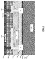
- FIG. 1 illustrates an example semiconductor device including an example HFET using an example shield wrap according to an embodiment of the present invention.
- the example HFET is formed on a substrate (omitted from FIG. 1 for simplicity).
- a buffer layer 100 is formed as a GaN film.
- Another semiconductor film 102 is placed over the surface of buffer layer 100 to form a heterostructure with buffer layer 100.
- Semiconductor film 102 creates a conduction channel at the top portion of buffer layer 100.
- semiconductor film 102 may be AlGaN.
- FETs not shown, including non-heterostructure FETs
- semiconductor film 102 may be other materials, may be omitted, or may be the same material as buffer layer 100.
- buffer layer 100 may be made of other materials, such as silicon, gallium arsenide (GaAs), indium phosphide (InP), SiC, and the like.
- buffer layer 100 and/or semiconductor film 102 may be a composite film made of layers of multiple films.
- a passivation film 104 is formed over semiconductor film 102.
- Passivation film 104 may form a portion of the gate dielectric and may be grown as a high-quality insulating material.
- passivation film 104 may be made of materials such as Al 2 O 3 , zirconium dioxide (ZrO 2 ), aluminum nitride (AlN), hafnium oxide (HfO 2 ), silicon dioxide (SiO 2 ), silicon nitride (Si 3 N 4 ), or other suitable gate dielectric materials.
- Passivation film 104 may also form a high-quality interface with semiconductor film 102, which may improve reliability and increase surface mobility of electrons, thereby improving device performance.
- Passivation film 104 may be formed as a low-defect/low-trap density film, which allows for improved gate dielectric reliability by minimizing the probability that hot carriers may be injected and/or trapped in passivation film 104.
- an atomic layer deposition ALD may be used to form a high-quality material to serve as passivation film 104.
- a passivation film 106 is formed over passivation film 104. Like passivation film 104, passivation film 106 may also form a portion of the gate dielectric. Passivation film 106 may be formed in a similar manner as and with materials similar to those of passivation film 104. For example, an in situ ALD process may be used to form both passivation films 104 and 106 in the same ALD tool without exposing the substrate to the environment outside of the tool. The combined thickness of passivation film 104 and 106 may be, for example, from 5nm-20nm. For a more detailed explanation of a process for forming these films, see U.S. Patent Application No.
- Shield wraps may equally apply to the FETs disclosed in that application. In other example FETs, only a single passivation film (e.g., passivation film 104) is used.
- a source electrode 108 and a drain electrode 110 are formed on semiconductor film 102. In other example HFETs, these electrodes may also contact buffer layer 100 under semiconductor film 102. The area between source electrode 108 and drain electrode 110 forms an active region where a conduction channel may form and may be controlled by gate electrode 112, which is formed on top of passivation film 106. In other example FETs, gate electrode 112 may be formed directly on semiconductor film 102. Gate electrode 112 is configured to modulate the conduction channel in the active region. In other words, by changing the voltage on gate electrode 112, conduction through the channel in the active region may be controlled.
- the metal stack for these electrodes may include, for example, Al, Ni, Ti, TiW, TiN, TiAu, TiAlMoAu, TiAlNiAu, TiAlPtAu, or the like. Other conductive materials besides metals may also be used.
- a passivation film 114 is formed over source electrode 108, drain electrode 110, and gate electrode 112 to allow for formation of interconnects to the electrodes, one or more field plates (if being used), and a shield wrap.
- Passivation film 114 may be made of insulating materials such as silicon nitride, silicon oxide, and the like. In some cases passivation film 114 may be a composite film of multiple layers of different films.
- a gate field plate 116 is formed on top of passivation film 114.
- Gate field plate 116 is designed to spread the electrical field on the edge of gate electrode 116 closest to drain electrode 110. Spreading the electric field in this region of the HFET may reduce the probability that carriers may be injected into the gate dielectric (passivation layers 104 and 106) and may help improve the reliability of the HFET. In other example HFETs, gate field plates may be omitted. Gate field play 116 may be made from similar materials as the source, drain, or gate electrodes.
- a passivation film 118 is formed over gate field plate 116.
- a metal pattern 120 may be formed over passivation film 118.
- Metal pattern 120 may include another gate field plate and vias 122 to make electrical contact to electrodes. In other example HFETs, only one gate field plate may be used or more than two gate field plates may be used.
- Encapsulation film 124 is formed over metal pattern 120.
- Encapsulation film 124 may differ from passivation films 104, 106, 114, and 118 in that the defect/trap density of encapsulation film 124 is less important as compared to passivation films that are closer to semiconductor film 102. This allows encapsulation film 124 to be made of materials that may not be suitable for a passivation film. However, encapsulation film 124 may also be made from the same materials used for one or more of the passivation films.
- encapsulation film 124 may be silicon oxide, silicon nitride, glass (e.g., frit-on glass), organic dielectrics (e.g., polyimide or benzocyclobutene based dielectrics), or the like. In some cases, encapsulation film 124 may be a composite film made of layers of multiple films. Encapsulation film 124 is about 0.5 ⁇ m to 5 ⁇ m thick. In one example, encapsulation film 124 is 1 ⁇ m thick.
- a metal pattern 126 is formed over encapsulation film 124.
- Metal pattern 126 includes shield wrap 130, a drain connection 132, and vias 128.
- Drain connection 132 makes electrical contact through one or more of vias 128 to drain electrode 110.
- Shield wrap 130 makes electrical contact through one or more of vias 128 to source electrode 108.
- shield wrap 130 may not be designed to spread the electric field. Instead, shield wrap 130 may contain electromagnetic radiation generated by the HFET. In other words, shield wrap 130 differs from a gate field plate in that shield wrap 130 covers as much of the HFET as possible. Thus, the geometry of shield wrap 130 may not be optimized for spreading the electric field on the edge of gate electrode 112 closest to drain electrode 110.
- shield wrap 130 may extend to overlap as much of the surface of the HFET as possible without creating a DC electrical path between source electrode 108 and drain electrode 110. By overlapping all of or a portion of the HFET, shield wrap 130 may reduce the electromagnetic radiation transmitted outside of the HFET as well as electromagnetic radiation reflected back to the HFET. To reduce the capacitive coupling between shield wrap 130 to the metal and semiconductor layers below shield wrap 130, the thickness, d 2 , of encapsulation layer 124 may be increased.
- a gap 134 defined in metal pattern 126 may be designed with a width, d 3 , that is sufficiently wide so that shield wrap 130 will not short to drain connection 132 at high voltages.
- the active region between source electrode 108 and drain electrode 110 may have a width, d 1 , that is about 1 ⁇ m per 100V of switching voltage for the HFET (e.g., a 500V HFET would have a d 1 of about 5 ⁇ m).
- gap 134 is filled with silicon nitride (SiN) (which may only require about 1 ⁇ m of SiN per 500-600V of switching voltage), the width, d 3 , of gap 134 may be 5-6 times smaller or than d 1 (e.g., a 500V HFET would have a d 3 about 1 ⁇ m). In one case, d 3 is 15-20% of d 1 .
- Metal pattern 126 may be, for example, about 0.7 ⁇ m to 2 ⁇ m thick.
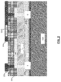
- FIG. 2 illustrates another example semiconductor device including an example HFET using an example shield wrap according to an embodiment of the present invention.
- a metal pattern 226 is formed over encapsulation film 224.
- Metal pattern 226 includes shield wrap 230, a source connection 232, and vias 228.
- Source connection 232 makes electrical contact through one or more of vias 228 to drain electrode 210.
- Shield wrap 230 makes electrical contact through one or more of vias 228 to source electrode 208.
- shield plate 230 may extend a distance d 3 past gate field plate 222.
- gate field plate 222 may also function as a portion of shield wrap 230 to maximize coverage of device surface.
- FIG. 3 illustrates a flow chart for an example process for making an example HFET having an example shield wrap according to an embodiment of the present invention. While various processing steps are included in the flow chart, it should be understood that other processing steps may be required to fabricate an example HFET with an example shield wrap according to an embodiment of the present invention. In other example processes, the steps shown in FIG. 3 may be performed in a different order or steps may be combined. For example, the gate electrode and a gate field plate may be formed at the same time. In still other example processes, some steps may be omitted. For example, an example process could omit the formation of the gate field plates if an HFET without gate field plates is desired.
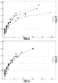
- FIGS. 4 and 5 depict experimental results for example HFETS without ( FIG. 4 ) and with ( FIG. 5 ) a shield wrap according to an embodiment of the present invention.
- FIGS. 4 and 5 depict I-V characteristics of an HFET with and without a shield wrap.
- the drain bias was set to various values as showing the legends of FIGS. 4 and 5 .
- the pulsing was performed with a 10ms period and 0.1% duty cycle.
- the total gate width was about 450 ⁇ m.
- the x-axis of FIGS. 4 and 5 are the instant drain voltage with the instant drain current on the y-axis.
- FIG. 4 shows that there is no distortion for drain voltages below 335V for the example HFET without a shield wrap
- FIG. 5 shows that there is not distortion for drain voltages below 365V for the example HFET with a shield wrap according to an embodiment of the present invention.
Landscapes
- Engineering & Computer Science (AREA)
- Microelectronics & Electronic Packaging (AREA)
- Power Engineering (AREA)
- Physics & Mathematics (AREA)
- Condensed Matter Physics & Semiconductors (AREA)
- General Physics & Mathematics (AREA)
- Computer Hardware Design (AREA)
- Ceramic Engineering (AREA)
- Junction Field-Effect Transistors (AREA)
- Insulated Gate Type Field-Effect Transistor (AREA)
Description
- The present disclosure relates generally to heterostructure field effect transistors (HFETs), and, more specifically, the present disclosure relates to a shield wrap for HFETs. 2. Background
- Many electrical devices such as cell phones, personal digital assistants (PDAs), laptops, etc., utilize power to operate. Because power is generally delivered through a wall socket as high-voltage alternating current (AC), a device, typically referred to as a power converter, can be utilized to transform the high-voltage AC input to a well-regulated direct current (DC) output through an energy transfer element. Switched-mode power converters are commonly used to improve efficiency and size and reduce component count in many of today's electronics. A switched- mode power converter may use a power switch that switches between a closed position (ON state) and an open position (OFF state) to transfer energy from an input to an output of the power converter. Typically, power switches are high-voltage devices required to withstand voltages substantially greater than the AC input voltage.
- One type of high-voltage field effect transistor (FET) used in switched-mode power converters is the HFET, also referred to as a high-electron mobility transistor (HEMT). HFETs may be used as switches in switching devices for high-voltage power electronics, such as power converters. In certain applications, HFETs based on wide-bandgap semiconductors may be useful because the higher bandgap may improve performance at elevated temperatures. Examples of wide-bandgap semiconductors used in high-voltage HFETs include materials such as silicon carbide (SiC), gallium nitride (GaN), and diamond, although other materials may be used as well.
-
U.S. Pat. Publ. No. 2006/0011915 A1 discloses a nitride semiconductor device comprising a non-doped first aluminum gallium nitride (AlxGa1-xN (0≦x≦1)) layer which is formed as a channel layer; a non-doped or n type second aluminum gallium nitride (AlyGa1-yN (0≦x≦1,x<y)) layer which is formed on the first aluminum gallium nitride layer as a barrier layer; an aluminum nitride (AlN) film which is formed on the second aluminum gallium nitride layer as a gate insulating film lower layer; an aluminum oxide (Al2O3) film which is formed on the aluminum nitride film as a gate insulating film upper layer; a source electrode and a drain electrode which are formed as first and second main electrodes to be electrically connected to the second aluminum gallium nitride layer, respectively; and a gate electrode which is formed on the aluminum oxide film as a control electrode.U.S. Pat. Publ. No. 2010/0314666 A1 discloses a nitride semiconductor device including a first layer made of a first nitride semiconductor; a second layer provided on the first layer and made of a second nitride semiconductor having a larger band gap than the first nitride semiconductor; a first electrode electrically connected to the second layer; a second electrode provided on the second layer and juxtaposed to the first electrode in a first direction; and a floating electrode provided on the second layer, the floating electrode including: a portion sandwiched by the second electrode in a second direction orthogonal to the first direction; and a portion protruding from the second electrode toward the first electrode. - The present invention relates to a semiconductor device as set out in claim 1. Preferred embodiments are described in the dependent claims.
- Various aspects, features, and advantages of several embodiments of the present invention will be more apparent from the following more particular description thereof, presented in conjunction with the following drawings.
- Non-limiting and non-exhaustive embodiments of the present invention are described with reference to the following Figures, wherein like reference numerals refer to like parts throughout the various views unless otherwise specified.
-
FIG. 1 illustrates an example HFET with a shield wrap according to an embodiment of the present invention. -
FIG. 2 illustrates another example HFET with a shield wrap. -
FIG. 3 illustrates a flowchart for an example process for creating an HFET with a shield wrap according to an embodiment of the present invention. -
FIG. 4 illustrates electrical results for an example HFET without a shield wrap according to an embodiment of the present invention. -
FIG. 5 illustrates electrical results for an example HFET with a shield wrap according to an embodiment of the present invention. - In the following description, numerous specific details are set forth in order to provide a thorough understanding of the present invention. It will be apparent, however, to one having ordinary skill in the art that the specific detail need not be employed to practice the present invention. In other instances, well-known materials or methods have not been described in detail in order to avoid obscuring the present invention.
- Reference throughout this specification to "one embodiment," "an embodiment," "one example," or "an example" means that a particular feature, structure or characteristic described in connection with the embodiment or example is included in at least one embodiment of the present invention. Thus, appearances of the phrases "in one embodiment," "in an embodiment," "one example," or "an example" in various places throughout this specification are not necessarily all referring to the same embodiment or example. Furthermore, the particular features, structures, or characteristics may be combined in any suitable combinations and/or subcombinations in one or more embodiments or examples. Particular features, structures, or characteristics may be included in an integrated circuit, an electronic circuit, a combinational logic circuit, or other suitable components that provide the described functionality. In addition, it is appreciated that the Figures provided herewith are for explanation purposes to persons ordinarily skilled in the art and that the drawings are not necessarily drawn to scale.
- In the description below, an example FET is used for the purposes of explanation. The example FET is referred to as an HFET despite the FET having a gate dielectric. In this respect, the example FET could also be called a metal insulator semiconductor FET (MISFET). Alternatively, the example FET could also be called a HEMT. For ease of explanation, however, the term HFET is used. It should be understood that use of these terms below are not limiting on the claims.
- As used in this application, an electrical connection is an ohmic connection. For example, two metal patterns that contact each through only metal are electrically connected. In contrast, the drain and source electrodes are not electrically connected because any connection between these electrodes is through a channel in the semiconductor and controlled by the gate electrode. Similarly, the gate electrode is not electrically connected to the semiconductor under the gate electrode when a gate dielectric is used to insulate the gate electrode from the semiconductor beneath.
- The operation of an HFET as a high-voltage switch involves ultra-fast (sub-microsecond) switching of the voltages of several hundreds volts. Such fast switching may generate large electromagnetic fields both near and far from the active region of the device. The frequency of these fields may be near the operating frequency of the HFET (e.g., in the kHz to MHz range). However, the channel of the HFET may experience local electromagnetic fields with much higher frequencies due to channel non-uniformities. These higher-frequency local fields may interact with contacts, pads, and metallization to emit in the GHz to THz range. Any of these large fields can be damaging and/or cause interference to surrounding circuits and even nearby electronic devices. The fields may also lead to long-term degradation and decreasing of the lifetime of packaging materials, interconnects, and dielectric layers exposed to the fields.
-
FIG. 1 illustrates an example semiconductor device including an example HFET using an example shield wrap according to an embodiment of the present invention. The example HFET is formed on a substrate (omitted fromFIG. 1 for simplicity). On the substrate, abuffer layer 100 is formed as a GaN film. Anothersemiconductor film 102 is placed over the surface ofbuffer layer 100 to form a heterostructure withbuffer layer 100.Semiconductor film 102 creates a conduction channel at the top portion ofbuffer layer 100. For example,semiconductor film 102 may be AlGaN. In other example FETs (not shown, including non-heterostructure FETs),semiconductor film 102 may be other materials, may be omitted, or may be the same material asbuffer layer 100. Similarly, in other example FETs (not shown),buffer layer 100 may be made of other materials, such as silicon, gallium arsenide (GaAs), indium phosphide (InP), SiC, and the like. In some cases,buffer layer 100 and/orsemiconductor film 102 may be a composite film made of layers of multiple films. - A
passivation film 104 is formed oversemiconductor film 102.Passivation film 104 may form a portion of the gate dielectric and may be grown as a high-quality insulating material. For example,passivation film 104 may be made of materials such as Al2O3, zirconium dioxide (ZrO2), aluminum nitride (AlN), hafnium oxide (HfO2), silicon dioxide (SiO2), silicon nitride (Si3N4), or other suitable gate dielectric materials.Passivation film 104 may also form a high-quality interface withsemiconductor film 102, which may improve reliability and increase surface mobility of electrons, thereby improving device performance. -
Passivation film 104 may be formed as a low-defect/low-trap density film, which allows for improved gate dielectric reliability by minimizing the probability that hot carriers may be injected and/or trapped inpassivation film 104. For example, an atomic layer deposition (ALD) may be used to form a high-quality material to serve aspassivation film 104. - A
passivation film 106 is formed overpassivation film 104. Likepassivation film 104,passivation film 106 may also form a portion of the gate dielectric.Passivation film 106 may be formed in a similar manner as and with materials similar to those ofpassivation film 104. For example, an in situ ALD process may be used to form bothpassivation films passivation film U.S. Patent Application No. 13/323,672, titled IN SITU GROWN GATE DIELECTRIC AND FIELD PLATE DIELECTRIC, filed December 12, 2011 - A
source electrode 108 and a drain electrode 110 are formed onsemiconductor film 102. In other example HFETs, these electrodes may also contactbuffer layer 100 undersemiconductor film 102. The area betweensource electrode 108 and drain electrode 110 forms an active region where a conduction channel may form and may be controlled by gate electrode 112, which is formed on top ofpassivation film 106. In other example FETs, gate electrode 112 may be formed directly onsemiconductor film 102. Gate electrode 112 is configured to modulate the conduction channel in the active region. In other words, by changing the voltage on gate electrode 112, conduction through the channel in the active region may be controlled. The metal stack for these electrodes may include, for example, Al, Ni, Ti, TiW, TiN, TiAu, TiAlMoAu, TiAlNiAu, TiAlPtAu, or the like. Other conductive materials besides metals may also be used. - A
passivation film 114 is formed oversource electrode 108, drain electrode 110, and gate electrode 112 to allow for formation of interconnects to the electrodes, one or more field plates (if being used), and a shield wrap.Passivation film 114 may be made of insulating materials such as silicon nitride, silicon oxide, and the like. In somecases passivation film 114 may be a composite film of multiple layers of different films. - A gate field plate 116 is formed on top of
passivation film 114. Gate field plate 116 is designed to spread the electrical field on the edge of gate electrode 116 closest to drain electrode 110. Spreading the electric field in this region of the HFET may reduce the probability that carriers may be injected into the gate dielectric (passivation layers 104 and 106) and may help improve the reliability of the HFET. In other example HFETs, gate field plates may be omitted. Gate field play 116 may be made from similar materials as the source, drain, or gate electrodes. - A
passivation film 118 is formed over gate field plate 116. Ametal pattern 120 may be formed overpassivation film 118.Metal pattern 120 may include another gate field plate and vias 122 to make electrical contact to electrodes. In other example HFETs, only one gate field plate may be used or more than two gate field plates may be used. - An
encapsulation film 124 is formed overmetal pattern 120.Encapsulation film 124 may differ frompassivation films encapsulation film 124 is less important as compared to passivation films that are closer tosemiconductor film 102. This allowsencapsulation film 124 to be made of materials that may not be suitable for a passivation film. However,encapsulation film 124 may also be made from the same materials used for one or more of the passivation films. For example,encapsulation film 124 may be silicon oxide, silicon nitride, glass (e.g., frit-on glass), organic dielectrics (e.g., polyimide or benzocyclobutene based dielectrics), or the like. In some cases,encapsulation film 124 may be a composite film made of layers of multiple films.Encapsulation film 124 is about 0.5 µm to 5 µm thick. In one example,encapsulation film 124 is 1 µm thick. - A
metal pattern 126 is formed overencapsulation film 124.Metal pattern 126 includesshield wrap 130, adrain connection 132, andvias 128.Drain connection 132 makes electrical contact through one or more ofvias 128 to drain electrode 110.Shield wrap 130 makes electrical contact through one or more ofvias 128 to sourceelectrode 108. In contrast to the field plates described above,shield wrap 130 may not be designed to spread the electric field. Instead, shieldwrap 130 may contain electromagnetic radiation generated by the HFET. In other words,shield wrap 130 differs from a gate field plate in that shield wrap 130 covers as much of the HFET as possible. Thus, the geometry ofshield wrap 130 may not be optimized for spreading the electric field on the edge of gate electrode 112 closest to drain electrode 110. In one example,shield wrap 130 may extend to overlap as much of the surface of the HFET as possible without creating a DC electrical path betweensource electrode 108 and drain electrode 110. By overlapping all of or a portion of the HFET,shield wrap 130 may reduce the electromagnetic radiation transmitted outside of the HFET as well as electromagnetic radiation reflected back to the HFET. To reduce the capacitive coupling between shield wrap 130 to the metal and semiconductor layers belowshield wrap 130, the thickness, d2, ofencapsulation layer 124 may be increased. - A gap 134 defined in
metal pattern 126 may be designed with a width, d3, that is sufficiently wide so thatshield wrap 130 will not short to drainconnection 132 at high voltages. For example, the active region betweensource electrode 108 and drain electrode 110 may have a width, d1, that is about 1 µm per 100V of switching voltage for the HFET (e.g., a 500V HFET would have a d1 of about 5 µm). In contrast, if gap 134 is filled with silicon nitride (SiN) (which may only require about 1 µm of SiN per 500-600V of switching voltage), the width, d3, of gap 134 may be 5-6 times smaller or than d1 (e.g., a 500V HFET would have a d3 about 1 µm). In one case, d3 is 15-20% of d1.Metal pattern 126 may be, for example, about 0.7 µm to 2 µm thick. -
FIG. 2 illustrates another example semiconductor device including an example HFET using an example shield wrap according to an embodiment of the present invention. As shown, a metal pattern 226 is formed overencapsulation film 224. Metal pattern 226 includesshield wrap 230, asource connection 232, and vias 228.Source connection 232 makes electrical contact through one or more of vias 228 to drainelectrode 210.Shield wrap 230 makes electrical contact through one or more of vias 228 to sourceelectrode 208. As shown,shield plate 230 may extend a distance d3 past gate field plate 222. In one example, gate field plate 222 may also function as a portion ofshield wrap 230 to maximize coverage of device surface. -
FIG. 3 illustrates a flow chart for an example process for making an example HFET having an example shield wrap according to an embodiment of the present invention. While various processing steps are included in the flow chart, it should be understood that other processing steps may be required to fabricate an example HFET with an example shield wrap according to an embodiment of the present invention. In other example processes, the steps shown inFIG. 3 may be performed in a different order or steps may be combined. For example, the gate electrode and a gate field plate may be formed at the same time. In still other example processes, some steps may be omitted. For example, an example process could omit the formation of the gate field plates if an HFET without gate field plates is desired. -
FIGS. 4 and 5 depict experimental results for example HFETS without (FIG. 4 ) and with (FIG. 5 ) a shield wrap according to an embodiment of the present invention. In particular,FIGS. 4 and 5 depict I-V characteristics of an HFET with and without a shield wrap. The results were obtained by pulsing an HEMT between the off state (gate bias = -10V) and the on state (gate bias = 0V). The drain bias was set to various values as showing the legends ofFIGS. 4 and 5 . The pulsing was performed with a 10ms period and 0.1% duty cycle. The total gate width was about 450 µm. The x-axis ofFIGS. 4 and 5 are the instant drain voltage with the instant drain current on the y-axis. - As is evident by comparing the results in
FIG. 4 (corresponding to the HFET without a shield wrap) to the results inFIG. 5 (corresponding to the HFET with a shield wrap according to an embodiment of the present invention), the distribution of instant drain current is more confined for the HFET with the shield wrap. A more confined distribution corresponds to an HFET with less degradation and better performance at higher drain voltages. Specifically,FIG. 4 shows that there is no distortion for drain voltages below 335V for the example HFET without a shield wrap, andFIG. 5 shows that there is not distortion for drain voltages below 365V for the example HFET with a shield wrap according to an embodiment of the present invention. - The above description of illustrated examples of the present invention, including what is described in the Abstract, are not intended to be exhaustive or to be limitations to the precise forms disclosed.
- These modifications can be made to examples of the invention in light of the above detailed description. The terms used in the following claims should not be construed to limit the invention to the specific embodiments disclosed in the specification and the claims. Rather, the scope is to be determined entirely by the following claims, which are to be construed in accordance with established doctrines of claim interpretation. The present specification and Figures are accordingly to be regarded as illustrative rather than restrictive.
Claims (15)
- A semiconductor device comprising:a substrate; and either:a buffer layer (100) on the substrate;a semiconductor film (102) on the buffer layer (100) configured to create a channel in the buffer layer (100); oran active region in a semiconductor film; the semiconductor device further comprising:a source electrode (108; 208) contacting the semiconductor film;a drain electrode (110; 210) contacting the semiconductor film, wherein an active region is between the source electrode and the drain electrode;a gate electrode (112) configured to modulate the channel in the active region;a first passivation film (104; 106; 114) over the semiconductor film;an encapsulation film (124; 224) over the first passivation film, wherein the encapsulation film (124; 224) is from 0.5 µm to 5 µm thick; anda shield wrap (130; 230) on the encapsulation film electrically connected to the source electrode (108; 208), wherein the shield wrap (130; 230) covers a majority of the active region.
- The semiconductor device of claim 1 further comprising:a heterostructure field effect transistor having the active region in the semiconductor film between the source electrode and the drain electrode, wherein the gate electrode (112) is over a portion of the active region; anda first metal pattern (130, 132; 230, 232) on the encapsulation film (124; 224), wherein the first metal pattern includes the shield wrap (130; 230).
- The semiconductor device of claim 2, wherein a gap (134) is defined in the first metal pattern (130; 132), and wherein the gap (134) separates the shield wrap (130) from a portion (132) of the first metal pattern that is connected to the drain electrode (110).
- The semiconductor device of claim 2, wherein the gap (134) is not formed over the active region.
- The semiconductor device of claim 3, wherein a distance from the drain electrode (110) to the source electrode (108) is 5 to 6 times larger than a width of the gap (134).
- The semiconductor device of claim 2, further comprising:a first gate field plate (116) defined by a second metal pattern on the first passivation film (104; 106; 114).
- The semiconductor device of claim 6, further comprising:a second gate field plate (122, 222) defined by a third metal pattern on a second passivation film (118) that is between the first passivation film (104; 106; 114) and the encapsulation film (124; 224).
- The semiconductor device of claim 7, wherein the shield wrap (130) completely overlaps the first field plate (116).
- The semiconductor device of claim 1 or 2, wherein the shield wrap (130; 230) covers at least 75% of the active region, preferably wherein the shield wrap (130; 230) covers the entire active region.
- The semiconductor device of claim 6, wherein at least 75% of the active region is covered by the shield wrap (130; 230) or the second metal pattern (122; 222), individually or in combination,
preferably wherein the entire active region is covered by the shield wrap (130; 230) or the second metal pattern (122; 222), individually or in combination. - The semiconductor device of claim 1, wherein the first passivation film (106; 108; 114) is a plurality of passivation films.
- The semiconductor device of claim 2, wherein the first metal pattern (130, 132; 230, 232) is in a metal layer that is the furthest metal layer away from the active region.
- The semiconductor device of claim 1 further comprising:one or more passivation films between the first passivation film and the encapsulation film (124; 224); anda first gate field plate (116) on the first passivation film or on a passivation film of the one or more passivation films between the first passivation film and the encapsulation film.
- The semiconductor device of claim 13 further comprising:a second gate field plate (122; 222) on a passivation film of the one ormore passivation films between the first passivation film and the encapsulation film.
- The semiconductor device of claim 1, wherein the gate electrode (112) is on the first passivation film (104; 106; 114).
Applications Claiming Priority (1)
| Application Number | Priority Date | Filing Date | Title |
|---|---|---|---|
| US13/333,843 US10002957B2 (en) | 2011-12-21 | 2011-12-21 | Shield wrap for a heterostructure field effect transistor |
Publications (2)
| Publication Number | Publication Date |
|---|---|
| EP2608271A1 EP2608271A1 (en) | 2013-06-26 |
| EP2608271B1 true EP2608271B1 (en) | 2016-10-19 |
Family
ID=47749594
Family Applications (1)
| Application Number | Title | Priority Date | Filing Date |
|---|---|---|---|
| EP12195320.2A Active EP2608271B1 (en) | 2011-12-21 | 2012-12-03 | Shield Wrap for a Heterostructure Field Effect Transistor |
Country Status (5)
| Country | Link |
|---|---|
| US (3) | US10002957B2 (en) |
| EP (1) | EP2608271B1 (en) |
| JP (1) | JP6644456B2 (en) |
| CN (1) | CN103178106B (en) |
| TW (1) | TWI496286B (en) |
Families Citing this family (23)
| Publication number | Priority date | Publication date | Assignee | Title |
|---|---|---|---|---|
| US10002957B2 (en) | 2011-12-21 | 2018-06-19 | Power Integrations, Inc. | Shield wrap for a heterostructure field effect transistor |
| US9443941B2 (en) * | 2012-06-04 | 2016-09-13 | Infineon Technologies Austria Ag | Compound semiconductor transistor with self aligned gate |
| JP2014082233A (en) * | 2012-10-12 | 2014-05-08 | Sumitomo Electric Ind Ltd | Semiconductor device and method of manufacturing the same |
| TWI577022B (en) | 2014-02-27 | 2017-04-01 | 台達電子工業股份有限公司 | Semiconductor device and semiconductor device package using the same |
| US10833185B2 (en) | 2013-09-10 | 2020-11-10 | Delta Electronics, Inc. | Heterojunction semiconductor device having source and drain pads with improved current crowding |
| US10236236B2 (en) | 2013-09-10 | 2019-03-19 | Delta Electronics, Inc. | Heterojunction semiconductor device for reducing parasitic capacitance |
| US10665709B2 (en) | 2013-09-10 | 2020-05-26 | Delta Electronics, Inc. | Power semiconductor device integrated with ESD protection circuit under source pad, drain pad, and/or gate pad |
| US10910491B2 (en) | 2013-09-10 | 2021-02-02 | Delta Electronics, Inc. | Semiconductor device having reduced capacitance between source and drain pads |
| JP6230456B2 (en) * | 2014-03-19 | 2017-11-15 | 株式会社東芝 | Semiconductor device |
| US20150340483A1 (en) * | 2014-05-21 | 2015-11-26 | International Rectifier Corporation | Group III-V Device Including a Shield Plate |
| JP6879662B2 (en) * | 2014-12-23 | 2021-06-02 | パワー・インテグレーションズ・インコーポレーテッド | High electron mobility transistor |
| US9543402B1 (en) | 2015-08-04 | 2017-01-10 | Power Integrations, Inc. | Integrated high performance lateral schottky diode |
| US10056478B2 (en) | 2015-11-06 | 2018-08-21 | Taiwan Semiconductor Manufacturing Company Ltd. | High-electron-mobility transistor and manufacturing method thereof |
| US9871067B2 (en) * | 2015-11-17 | 2018-01-16 | Taiwan Semiconductor Manufacturing Co., Ltd. | Infrared image sensor component |
| US9722063B1 (en) | 2016-04-11 | 2017-08-01 | Power Integrations, Inc. | Protective insulator for HFET devices |
| JP6233547B1 (en) * | 2016-10-24 | 2017-11-22 | 三菱電機株式会社 | Compound semiconductor devices |
| JP7154015B2 (en) * | 2017-03-03 | 2022-10-17 | パワー・インテグレーションズ・インコーポレーテッド | Switching device including charge distribution structure |
| US10680090B2 (en) * | 2017-07-20 | 2020-06-09 | Delta Electronics, Inc. | Enclosed gate runner for eliminating miller turn-on |
| US10204791B1 (en) * | 2017-09-22 | 2019-02-12 | Power Integrations, Inc. | Contact plug for high-voltage devices |
| JP7208167B2 (en) | 2018-01-19 | 2023-01-18 | ローム株式会社 | Semiconductor device and its manufacturing method |
| US10770391B2 (en) | 2018-03-27 | 2020-09-08 | Qualcomm Incorporated | Transistor with gate extension to limit second gate effect |
| JP6924166B2 (en) * | 2018-05-14 | 2021-08-25 | 株式会社東芝 | Semiconductor device |
| US20240030156A1 (en) * | 2021-08-11 | 2024-01-25 | Innoscience (suzhou) Semiconductor Co., Ltd. | Semiconductor device and method for manufacturing the same |
Family Cites Families (69)
| Publication number | Priority date | Publication date | Assignee | Title |
|---|---|---|---|---|
| JPS5368581A (en) * | 1976-12-01 | 1978-06-19 | Hitachi Ltd | Semiconductor device |
| JPS63266854A (en) | 1987-04-23 | 1988-11-02 | Ricoh Co Ltd | Semiconductor integrated circuit device |
| JP3139783B2 (en) | 1991-08-22 | 2001-03-05 | 株式会社東芝 | Semiconductor integrated circuit device |
| JPH05152291A (en) | 1991-11-29 | 1993-06-18 | Mitsubishi Electric Corp | Semiconductor integrated circuit device |
| JPH08330519A (en) | 1995-06-01 | 1996-12-13 | Hitachi Ltd | Compound semiconductor integrated circuit device |
| KR100244282B1 (en) * | 1997-08-25 | 2000-02-01 | 김영환 | Transistor for high voltage and manufactruing method thereof |
| US6127703A (en) * | 1999-08-31 | 2000-10-03 | Philips Electronics North America Corporation | Lateral thin-film silicon-on-insulator (SOI) PMOS device having a drain extension region |
| CN1557024B (en) * | 2001-07-24 | 2010-04-07 | 美商克立股份有限公司 | Insulting gate Al Ga nitride/GaN HEMT |
| US7898047B2 (en) * | 2003-03-03 | 2011-03-01 | Samsung Electronics Co., Ltd. | Integrated nitride and silicon carbide-based devices and methods of fabricating integrated nitride-based devices |
| US7501669B2 (en) | 2003-09-09 | 2009-03-10 | Cree, Inc. | Wide bandgap transistor devices with field plates |
| JP4417677B2 (en) * | 2003-09-19 | 2010-02-17 | 株式会社東芝 | Power semiconductor device |
| JP4041075B2 (en) * | 2004-02-27 | 2008-01-30 | 株式会社東芝 | Semiconductor device |
| US7573078B2 (en) * | 2004-05-11 | 2009-08-11 | Cree, Inc. | Wide bandgap transistors with multiple field plates |
| US7550783B2 (en) * | 2004-05-11 | 2009-06-23 | Cree, Inc. | Wide bandgap HEMTs with source connected field plates |
| US7148540B2 (en) * | 2004-06-28 | 2006-12-12 | Agere Systems Inc. | Graded conductive structure for use in a metal-oxide-semiconductor device |
| JP2006032552A (en) | 2004-07-14 | 2006-02-02 | Toshiba Corp | Semiconductor device containing nitride |
| US7355215B2 (en) * | 2004-12-06 | 2008-04-08 | Cree, Inc. | Field effect transistors (FETs) having multi-watt output power at millimeter-wave frequencies |
| US7800131B2 (en) * | 2005-06-10 | 2010-09-21 | Nec Corporation | Field effect transistor |
| US7855401B2 (en) * | 2005-06-29 | 2010-12-21 | Cree, Inc. | Passivation of wide band-gap based semiconductor devices with hydrogen-free sputtered nitrides |
| US8692324B2 (en) * | 2005-07-13 | 2014-04-08 | Ciclon Semiconductor Device Corp. | Semiconductor devices having charge balanced structure |
| JP4751150B2 (en) * | 2005-08-31 | 2011-08-17 | 株式会社東芝 | Nitride semiconductor devices |
| JP5124839B2 (en) | 2005-09-28 | 2013-01-23 | 株式会社リキッド・デザイン・システムズ | Semiconductor device |
| JP2007157829A (en) * | 2005-12-01 | 2007-06-21 | Matsushita Electric Ind Co Ltd | Semiconductor device |
| US9608102B2 (en) * | 2005-12-02 | 2017-03-28 | Infineon Technologies Americas Corp. | Gallium nitride material devices and associated methods |
| US7566913B2 (en) * | 2005-12-02 | 2009-07-28 | Nitronex Corporation | Gallium nitride material devices including conductive regions and methods associated with the same |
| TW200735361A (en) * | 2005-12-14 | 2007-09-16 | Koninkl Philips Electronics Nv | MOS transistor and a method of manufacturing a MOS transistor |
| US7388236B2 (en) * | 2006-03-29 | 2008-06-17 | Cree, Inc. | High efficiency and/or high power density wide bandgap transistors |
| US7629627B2 (en) * | 2006-04-18 | 2009-12-08 | University Of Massachusetts | Field effect transistor with independently biased gates |
| JP5065616B2 (en) * | 2006-04-21 | 2012-11-07 | 株式会社東芝 | Nitride semiconductor device |
| US7656010B2 (en) * | 2006-09-20 | 2010-02-02 | Panasonic Corporation | Semiconductor device |
| KR100782430B1 (en) * | 2006-09-22 | 2007-12-05 | 한국과학기술원 | Gan-hemt (high electron mobility transistor) structure with inner field-plate structure for high power applications |
| JP5186096B2 (en) * | 2006-10-12 | 2013-04-17 | パナソニック株式会社 | Nitride semiconductor transistor and manufacturing method thereof |
| JP2008130655A (en) * | 2006-11-17 | 2008-06-05 | Toshiba Corp | Semiconductor element |
| US8878245B2 (en) * | 2006-11-30 | 2014-11-04 | Cree, Inc. | Transistors and method for making ohmic contact to transistors |
| US8154079B2 (en) * | 2006-12-07 | 2012-04-10 | Kabushiki Kaisha Toshiba | Semiconductor device and fabrication method of the semiconductor device |
| US7952145B2 (en) * | 2007-02-20 | 2011-05-31 | Texas Instruments Lehigh Valley Incorporated | MOS transistor device in common source configuration |
| JP2008277604A (en) | 2007-05-01 | 2008-11-13 | Oki Electric Ind Co Ltd | Field-effect transistor |
| WO2009073866A1 (en) * | 2007-12-07 | 2009-06-11 | The Government Of The United States Of America, As Represented By The Secretary Of The Navy | Gate after diamond transistor |
| US8519438B2 (en) * | 2008-04-23 | 2013-08-27 | Transphorm Inc. | Enhancement mode III-N HEMTs |
| JP2010118556A (en) * | 2008-11-13 | 2010-05-27 | Furukawa Electric Co Ltd:The | Semiconductor device and its manufacturing method |
| US7884394B2 (en) * | 2009-02-09 | 2011-02-08 | Transphorm Inc. | III-nitride devices and circuits |
| JP2010219117A (en) * | 2009-03-13 | 2010-09-30 | Toshiba Corp | Semiconductor device |
| US8754496B2 (en) * | 2009-04-14 | 2014-06-17 | Triquint Semiconductor, Inc. | Field effect transistor having a plurality of field plates |
| US8008977B2 (en) * | 2009-04-14 | 2011-08-30 | Triquint Semiconductor, Inc. | Field-plated transistor including feedback resistor |
| DE102009018054B4 (en) * | 2009-04-21 | 2018-11-29 | Infineon Technologies Austria Ag | Lateral HEMT and method of making a lateral HEMT |
| JP5481103B2 (en) | 2009-06-11 | 2014-04-23 | 株式会社東芝 | Nitride semiconductor device |
| JP4794656B2 (en) * | 2009-06-11 | 2011-10-19 | シャープ株式会社 | Semiconductor device |
| US8384129B2 (en) * | 2009-06-25 | 2013-02-26 | The United States Of America, As Represented By The Secretary Of The Navy | Transistor with enhanced channel charge inducing material layer and threshold voltage control |
| US9991360B2 (en) * | 2009-06-26 | 2018-06-05 | Cornell University | Method for forming III-V semiconductor structures including aluminum-silicon nitride passivation |
| US8390000B2 (en) * | 2009-08-28 | 2013-03-05 | Transphorm Inc. | Semiconductor devices with field plates |
| US8338860B2 (en) * | 2009-10-30 | 2012-12-25 | Alpha And Omega Semiconductor Incorporated | Normally off gallium nitride field effect transistors (FET) |
| JP5703565B2 (en) * | 2010-01-12 | 2015-04-22 | 住友電気工業株式会社 | Compound semiconductor device |
| US8829999B2 (en) * | 2010-05-20 | 2014-09-09 | Cree, Inc. | Low noise amplifiers including group III nitride based high electron mobility transistors |
| US8772832B2 (en) * | 2010-06-04 | 2014-07-08 | Hrl Laboratories, Llc | GaN HEMTs with a back gate connected to the source |
| US8368121B2 (en) * | 2010-06-21 | 2013-02-05 | Power Integrations, Inc. | Enhancement-mode HFET circuit arrangement having high power and high threshold voltage |
| CN102576727B (en) * | 2010-06-23 | 2016-01-27 | 康奈尔大学 | Gated III-V semiconductor structure and method |
| JP5649347B2 (en) * | 2010-07-20 | 2015-01-07 | 住友電工デバイス・イノベーション株式会社 | Semiconductor device |
| JP2012109492A (en) * | 2010-11-19 | 2012-06-07 | Sanken Electric Co Ltd | Compound semiconductor device |
| JP5758132B2 (en) * | 2011-01-26 | 2015-08-05 | 株式会社東芝 | Semiconductor element |
| JP5776217B2 (en) * | 2011-02-24 | 2015-09-09 | 富士通株式会社 | Compound semiconductor device |
| JP5866773B2 (en) * | 2011-02-25 | 2016-02-17 | 富士通株式会社 | Compound semiconductor device and manufacturing method thereof |
| US8716141B2 (en) * | 2011-03-04 | 2014-05-06 | Transphorm Inc. | Electrode configurations for semiconductor devices |
| US9093432B2 (en) * | 2011-09-23 | 2015-07-28 | Sanken Electric Co., Ltd. | Semiconductor device |
| US20130087803A1 (en) * | 2011-10-06 | 2013-04-11 | Epowersoft, Inc. | Monolithically integrated hemt and schottky diode |
| US20130099284A1 (en) * | 2011-10-20 | 2013-04-25 | Triquint Semiconductor, Inc. | Group iii-nitride metal-insulator-semiconductor heterostructure field-effect transistors |
| US8633094B2 (en) * | 2011-12-01 | 2014-01-21 | Power Integrations, Inc. | GaN high voltage HFET with passivation plus gate dielectric multilayer structure |
| US20130146943A1 (en) | 2011-12-12 | 2013-06-13 | John P. EDWARDS | In situ grown gate dielectric and field plate dielectric |
| US10002957B2 (en) | 2011-12-21 | 2018-06-19 | Power Integrations, Inc. | Shield wrap for a heterostructure field effect transistor |
| US9306014B1 (en) * | 2013-12-27 | 2016-04-05 | Power Integrations, Inc. | High-electron-mobility transistors |
-
2011
- 2011-12-21 US US13/333,843 patent/US10002957B2/en active Active
-
2012
- 2012-12-03 EP EP12195320.2A patent/EP2608271B1/en active Active
- 2012-12-18 CN CN201210552008.XA patent/CN103178106B/en active Active
- 2012-12-20 TW TW101148577A patent/TWI496286B/en active
- 2012-12-20 JP JP2012278136A patent/JP6644456B2/en active Active
-
2016
- 2016-12-21 US US15/387,510 patent/US10199488B2/en active Active
-
2018
- 2018-12-20 US US16/228,159 patent/US20190214493A1/en not_active Abandoned
Also Published As
| Publication number | Publication date |
|---|---|
| US20130161692A1 (en) | 2013-06-27 |
| TWI496286B (en) | 2015-08-11 |
| EP2608271A1 (en) | 2013-06-26 |
| US10002957B2 (en) | 2018-06-19 |
| US10199488B2 (en) | 2019-02-05 |
| CN103178106A (en) | 2013-06-26 |
| TW201342594A (en) | 2013-10-16 |
| CN103178106B (en) | 2016-10-05 |
| US20190214493A1 (en) | 2019-07-11 |
| JP2013131758A (en) | 2013-07-04 |
| US20170098704A1 (en) | 2017-04-06 |
| JP6644456B2 (en) | 2020-02-12 |
Similar Documents
| Publication | Publication Date | Title |
|---|---|---|
| EP2608271B1 (en) | Shield Wrap for a Heterostructure Field Effect Transistor | |
| US11721753B2 (en) | Method of fabricating a transistor | |
| KR101992565B1 (en) | High-electron-mobility transistor and manufacturing method thereof | |
| CN104835847B (en) | Semiconductor device with a plurality of transistors | |
| KR101527647B1 (en) | A heterostructure semiconductor device and a method of fabricating a heterostructure semiconductor device | |
| Saito et al. | Design optimization of high breakdown voltage AlGaN-GaN power HEMT on an insulating substrate for R/sub ON/AV/sub B/tradeoff characteristics | |
| US20090072269A1 (en) | Gallium nitride diodes and integrated components | |
| US9190510B2 (en) | Semiconductor device with breakdown preventing layer | |
| US11114539B2 (en) | Gate stack for heterostructure device | |
| US10103239B1 (en) | High electron mobility transistor structure | |
| WO2018087728A1 (en) | Semiconductor devices with multiple channels and three-dimensional electrodes | |
| US9543402B1 (en) | Integrated high performance lateral schottky diode | |
| KR20240013239A (en) | Multilayer encapsulation and related fabrication methods for moisture robustness and highly accelerated stress tests |
Legal Events
| Date | Code | Title | Description |
|---|---|---|---|
| 17P | Request for examination filed |
Effective date: 20121203 |
|
| AK | Designated contracting states |
Kind code of ref document: A1 Designated state(s): AL AT BE BG CH CY CZ DE DK EE ES FI FR GB GR HR HU IE IS IT LI LT LU LV MC MK MT NL NO PL PT RO RS SE SI SK SM TR |
|
| AX | Request for extension of the european patent |
Extension state: BA ME |
|
| PUAI | Public reference made under article 153(3) epc to a published international application that has entered the european phase |
Free format text: ORIGINAL CODE: 0009012 |
|
| 17Q | First examination report despatched |
Effective date: 20130603 |
|
| GRAP | Despatch of communication of intention to grant a patent |
Free format text: ORIGINAL CODE: EPIDOSNIGR1 |
|
| INTG | Intention to grant announced |
Effective date: 20160603 |
|
| GRAS | Grant fee paid |
Free format text: ORIGINAL CODE: EPIDOSNIGR3 |
|
| GRAA | (expected) grant |
Free format text: ORIGINAL CODE: 0009210 |
|
| AK | Designated contracting states |
Kind code of ref document: B1 Designated state(s): AL AT BE BG CH CY CZ DE DK EE ES FI FR GB GR HR HU IE IS IT LI LT LU LV MC MK MT NL NO PL PT RO RS SE SI SK SM TR |
|
| REG | Reference to a national code |
Ref country code: GB Ref legal event code: FG4D |
|
| REG | Reference to a national code |
Ref country code: CH Ref legal event code: EP |
|
| REG | Reference to a national code |
Ref country code: AT Ref legal event code: REF Ref document number: 838988 Country of ref document: AT Kind code of ref document: T Effective date: 20161115 |
|
| REG | Reference to a national code |
Ref country code: IE Ref legal event code: FG4D |
|
| REG | Reference to a national code |
Ref country code: DE Ref legal event code: R096 Ref document number: 602012024269 Country of ref document: DE |
|
| REG | Reference to a national code |
Ref country code: FR Ref legal event code: PLFP Year of fee payment: 5 |
|
| REG | Reference to a national code |
Ref country code: NL Ref legal event code: MP Effective date: 20161019 |
|
| REG | Reference to a national code |
Ref country code: LT Ref legal event code: MG4D |
|
| PG25 | Lapsed in a contracting state [announced via postgrant information from national office to epo] |
Ref country code: LV Free format text: LAPSE BECAUSE OF FAILURE TO SUBMIT A TRANSLATION OF THE DESCRIPTION OR TO PAY THE FEE WITHIN THE PRESCRIBED TIME-LIMIT Effective date: 20161019 |
|
| REG | Reference to a national code |
Ref country code: AT Ref legal event code: MK05 Ref document number: 838988 Country of ref document: AT Kind code of ref document: T Effective date: 20161019 |
|
| PG25 | Lapsed in a contracting state [announced via postgrant information from national office to epo] |
Ref country code: GR Free format text: LAPSE BECAUSE OF FAILURE TO SUBMIT A TRANSLATION OF THE DESCRIPTION OR TO PAY THE FEE WITHIN THE PRESCRIBED TIME-LIMIT Effective date: 20170120 Ref country code: LT Free format text: LAPSE BECAUSE OF FAILURE TO SUBMIT A TRANSLATION OF THE DESCRIPTION OR TO PAY THE FEE WITHIN THE PRESCRIBED TIME-LIMIT Effective date: 20161019 Ref country code: SE Free format text: LAPSE BECAUSE OF FAILURE TO SUBMIT A TRANSLATION OF THE DESCRIPTION OR TO PAY THE FEE WITHIN THE PRESCRIBED TIME-LIMIT Effective date: 20161019 Ref country code: NO Free format text: LAPSE BECAUSE OF FAILURE TO SUBMIT A TRANSLATION OF THE DESCRIPTION OR TO PAY THE FEE WITHIN THE PRESCRIBED TIME-LIMIT Effective date: 20170119 |
|
| PG25 | Lapsed in a contracting state [announced via postgrant information from national office to epo] |
Ref country code: HR Free format text: LAPSE BECAUSE OF FAILURE TO SUBMIT A TRANSLATION OF THE DESCRIPTION OR TO PAY THE FEE WITHIN THE PRESCRIBED TIME-LIMIT Effective date: 20161019 Ref country code: AT Free format text: LAPSE BECAUSE OF FAILURE TO SUBMIT A TRANSLATION OF THE DESCRIPTION OR TO PAY THE FEE WITHIN THE PRESCRIBED TIME-LIMIT Effective date: 20161019 Ref country code: PT Free format text: LAPSE BECAUSE OF FAILURE TO SUBMIT A TRANSLATION OF THE DESCRIPTION OR TO PAY THE FEE WITHIN THE PRESCRIBED TIME-LIMIT Effective date: 20170220 Ref country code: FI Free format text: LAPSE BECAUSE OF FAILURE TO SUBMIT A TRANSLATION OF THE DESCRIPTION OR TO PAY THE FEE WITHIN THE PRESCRIBED TIME-LIMIT Effective date: 20161019 Ref country code: NL Free format text: LAPSE BECAUSE OF FAILURE TO SUBMIT A TRANSLATION OF THE DESCRIPTION OR TO PAY THE FEE WITHIN THE PRESCRIBED TIME-LIMIT Effective date: 20161019 Ref country code: PL Free format text: LAPSE BECAUSE OF FAILURE TO SUBMIT A TRANSLATION OF THE DESCRIPTION OR TO PAY THE FEE WITHIN THE PRESCRIBED TIME-LIMIT Effective date: 20161019 Ref country code: IS Free format text: LAPSE BECAUSE OF FAILURE TO SUBMIT A TRANSLATION OF THE DESCRIPTION OR TO PAY THE FEE WITHIN THE PRESCRIBED TIME-LIMIT Effective date: 20170219 Ref country code: RS Free format text: LAPSE BECAUSE OF FAILURE TO SUBMIT A TRANSLATION OF THE DESCRIPTION OR TO PAY THE FEE WITHIN THE PRESCRIBED TIME-LIMIT Effective date: 20161019 Ref country code: ES Free format text: LAPSE BECAUSE OF FAILURE TO SUBMIT A TRANSLATION OF THE DESCRIPTION OR TO PAY THE FEE WITHIN THE PRESCRIBED TIME-LIMIT Effective date: 20161019 |
|
| REG | Reference to a national code |
Ref country code: DE Ref legal event code: R097 Ref document number: 602012024269 Country of ref document: DE |
|
| PG25 | Lapsed in a contracting state [announced via postgrant information from national office to epo] |
Ref country code: DK Free format text: LAPSE BECAUSE OF FAILURE TO SUBMIT A TRANSLATION OF THE DESCRIPTION OR TO PAY THE FEE WITHIN THE PRESCRIBED TIME-LIMIT Effective date: 20161019 Ref country code: RO Free format text: LAPSE BECAUSE OF FAILURE TO SUBMIT A TRANSLATION OF THE DESCRIPTION OR TO PAY THE FEE WITHIN THE PRESCRIBED TIME-LIMIT Effective date: 20161019 Ref country code: EE Free format text: LAPSE BECAUSE OF FAILURE TO SUBMIT A TRANSLATION OF THE DESCRIPTION OR TO PAY THE FEE WITHIN THE PRESCRIBED TIME-LIMIT Effective date: 20161019 Ref country code: CZ Free format text: LAPSE BECAUSE OF FAILURE TO SUBMIT A TRANSLATION OF THE DESCRIPTION OR TO PAY THE FEE WITHIN THE PRESCRIBED TIME-LIMIT Effective date: 20161019 Ref country code: SK Free format text: LAPSE BECAUSE OF FAILURE TO SUBMIT A TRANSLATION OF THE DESCRIPTION OR TO PAY THE FEE WITHIN THE PRESCRIBED TIME-LIMIT Effective date: 20161019 |
|
| REG | Reference to a national code |
Ref country code: CH Ref legal event code: PL |
|
| PLBE | No opposition filed within time limit |
Free format text: ORIGINAL CODE: 0009261 |
|
| STAA | Information on the status of an ep patent application or granted ep patent |
Free format text: STATUS: NO OPPOSITION FILED WITHIN TIME LIMIT |
|
| PG25 | Lapsed in a contracting state [announced via postgrant information from national office to epo] |
Ref country code: SM Free format text: LAPSE BECAUSE OF FAILURE TO SUBMIT A TRANSLATION OF THE DESCRIPTION OR TO PAY THE FEE WITHIN THE PRESCRIBED TIME-LIMIT Effective date: 20161019 Ref country code: BG Free format text: LAPSE BECAUSE OF FAILURE TO SUBMIT A TRANSLATION OF THE DESCRIPTION OR TO PAY THE FEE WITHIN THE PRESCRIBED TIME-LIMIT Effective date: 20170119 Ref country code: IT Free format text: LAPSE BECAUSE OF FAILURE TO SUBMIT A TRANSLATION OF THE DESCRIPTION OR TO PAY THE FEE WITHIN THE PRESCRIBED TIME-LIMIT Effective date: 20161019 |
|
| 26N | No opposition filed |
Effective date: 20170720 |
|
| GBPC | Gb: european patent ceased through non-payment of renewal fee |
Effective date: 20170119 |
|
| PG25 | Lapsed in a contracting state [announced via postgrant information from national office to epo] |
Ref country code: MC Free format text: LAPSE BECAUSE OF FAILURE TO SUBMIT A TRANSLATION OF THE DESCRIPTION OR TO PAY THE FEE WITHIN THE PRESCRIBED TIME-LIMIT Effective date: 20161019 |
|
| REG | Reference to a national code |
Ref country code: IE Ref legal event code: MM4A |
|
| PG25 | Lapsed in a contracting state [announced via postgrant information from national office to epo] |
Ref country code: LU Free format text: LAPSE BECAUSE OF NON-PAYMENT OF DUE FEES Effective date: 20161203 Ref country code: LI Free format text: LAPSE BECAUSE OF NON-PAYMENT OF DUE FEES Effective date: 20161231 Ref country code: CH Free format text: LAPSE BECAUSE OF NON-PAYMENT OF DUE FEES Effective date: 20161231 |
|
| PG25 | Lapsed in a contracting state [announced via postgrant information from national office to epo] |
Ref country code: GB Free format text: LAPSE BECAUSE OF NON-PAYMENT OF DUE FEES Effective date: 20170119 Ref country code: IE Free format text: LAPSE BECAUSE OF NON-PAYMENT OF DUE FEES Effective date: 20161203 Ref country code: SI Free format text: LAPSE BECAUSE OF FAILURE TO SUBMIT A TRANSLATION OF THE DESCRIPTION OR TO PAY THE FEE WITHIN THE PRESCRIBED TIME-LIMIT Effective date: 20161019 |
|
| REG | Reference to a national code |
Ref country code: FR Ref legal event code: PLFP Year of fee payment: 6 |
|
| PG25 | Lapsed in a contracting state [announced via postgrant information from national office to epo] |
Ref country code: CY Free format text: LAPSE BECAUSE OF FAILURE TO SUBMIT A TRANSLATION OF THE DESCRIPTION OR TO PAY THE FEE WITHIN THE PRESCRIBED TIME-LIMIT Effective date: 20161019 Ref country code: HU Free format text: LAPSE BECAUSE OF FAILURE TO SUBMIT A TRANSLATION OF THE DESCRIPTION OR TO PAY THE FEE WITHIN THE PRESCRIBED TIME-LIMIT; INVALID AB INITIO Effective date: 20121203 |
|
| PG25 | Lapsed in a contracting state [announced via postgrant information from national office to epo] |
Ref country code: TR Free format text: LAPSE BECAUSE OF FAILURE TO SUBMIT A TRANSLATION OF THE DESCRIPTION OR TO PAY THE FEE WITHIN THE PRESCRIBED TIME-LIMIT Effective date: 20161019 Ref country code: MK Free format text: LAPSE BECAUSE OF FAILURE TO SUBMIT A TRANSLATION OF THE DESCRIPTION OR TO PAY THE FEE WITHIN THE PRESCRIBED TIME-LIMIT Effective date: 20161019 |
|
| PG25 | Lapsed in a contracting state [announced via postgrant information from national office to epo] |
Ref country code: MT Free format text: LAPSE BECAUSE OF NON-PAYMENT OF DUE FEES Effective date: 20161203 |
|
| PG25 | Lapsed in a contracting state [announced via postgrant information from national office to epo] |
Ref country code: AL Free format text: LAPSE BECAUSE OF FAILURE TO SUBMIT A TRANSLATION OF THE DESCRIPTION OR TO PAY THE FEE WITHIN THE PRESCRIBED TIME-LIMIT Effective date: 20161019 |
|
| P01 | Opt-out of the competence of the unified patent court (upc) registered |
Effective date: 20230502 |
|
| PGFP | Annual fee paid to national office [announced via postgrant information from national office to epo] |
Ref country code: FR Payment date: 20231227 Year of fee payment: 12 |
|
| PGFP | Annual fee paid to national office [announced via postgrant information from national office to epo] |
Ref country code: BE Payment date: 20231227 Year of fee payment: 12 |
|
| PGFP | Annual fee paid to national office [announced via postgrant information from national office to epo] |
Ref country code: DE Payment date: 20231229 Year of fee payment: 12 |