EP2608049A1 - Control system and relay apparatus - Google Patents
Control system and relay apparatus Download PDFInfo
- Publication number
- EP2608049A1 EP2608049A1 EP20120192374 EP12192374A EP2608049A1 EP 2608049 A1 EP2608049 A1 EP 2608049A1 EP 20120192374 EP20120192374 EP 20120192374 EP 12192374 A EP12192374 A EP 12192374A EP 2608049 A1 EP2608049 A1 EP 2608049A1
- Authority
- EP
- European Patent Office
- Prior art keywords
- signal
- circuit
- reset
- output
- bus
- Prior art date
- Legal status (The legal status is an assumption and is not a legal conclusion. Google has not performed a legal analysis and makes no representation as to the accuracy of the status listed.)
- Granted
Links
Images







Classifications
-
- G—PHYSICS
- G06—COMPUTING OR CALCULATING; COUNTING
- G06F—ELECTRIC DIGITAL DATA PROCESSING
- G06F13/00—Interconnection of, or transfer of information or other signals between, memories, input/output devices or central processing units
- G06F13/38—Information transfer, e.g. on bus
- G06F13/42—Bus transfer protocol, e.g. handshake; Synchronisation
- G06F13/4282—Bus transfer protocol, e.g. handshake; Synchronisation on a serial bus, e.g. I2C bus, SPI bus
- G06F13/4291—Bus transfer protocol, e.g. handshake; Synchronisation on a serial bus, e.g. I2C bus, SPI bus using a clocked protocol
-
- G—PHYSICS
- G06—COMPUTING OR CALCULATING; COUNTING
- G06F—ELECTRIC DIGITAL DATA PROCESSING
- G06F13/00—Interconnection of, or transfer of information or other signals between, memories, input/output devices or central processing units
-
- G—PHYSICS
- G06—COMPUTING OR CALCULATING; COUNTING
- G06F—ELECTRIC DIGITAL DATA PROCESSING
- G06F1/00—Details not covered by groups G06F3/00 - G06F13/00 and G06F21/00
- G06F1/24—Resetting means
-
- G—PHYSICS
- G06—COMPUTING OR CALCULATING; COUNTING
- G06F—ELECTRIC DIGITAL DATA PROCESSING
- G06F13/00—Interconnection of, or transfer of information or other signals between, memories, input/output devices or central processing units
- G06F13/38—Information transfer, e.g. on bus
-
- G—PHYSICS
- G06—COMPUTING OR CALCULATING; COUNTING
- G06F—ELECTRIC DIGITAL DATA PROCESSING
- G06F13/00—Interconnection of, or transfer of information or other signals between, memories, input/output devices or central processing units
- G06F13/38—Information transfer, e.g. on bus
- G06F13/382—Information transfer, e.g. on bus using universal interface adapter
- G06F13/385—Information transfer, e.g. on bus using universal interface adapter for adaptation of a particular data processing system to different peripheral devices
-
- G—PHYSICS
- G06—COMPUTING OR CALCULATING; COUNTING
- G06F—ELECTRIC DIGITAL DATA PROCESSING
- G06F9/00—Arrangements for program control, e.g. control units
- G06F9/06—Arrangements for program control, e.g. control units using stored programs, i.e. using an internal store of processing equipment to receive or retain programs
- G06F9/44—Arrangements for executing specific programs
- G06F9/4401—Bootstrapping
- G06F9/4411—Configuring for operating with peripheral devices; Loading of device drivers
Definitions
- a control system that includes an electronic circuit; a bus interface configured to receive, via a bus, a control signal for controlling the electronic circuit, and output a signal corresponding to the received control signal to the electronic circuit; a signal maintaining circuit configured to maintain a value of the signal to be output from the bus interface to the electronic circuit; a reset control circuit configured to cause the signal maintaining circuit to maintain the value of the output signal to the electronic circuit, and subsequently reset the bus interface; and a control device configured to control the electronic circuit by outputting the control signal via the bus.
- the reset control circuit 14 is configured to, when the bus 31 becomes unusable, cause the signal maintaining circuit 13 to maintain the value of the output signal to the electronic circuit 11, and then resets the bus interface 12. When the bus interface 12 is reset, the bus 31 is restored to an operational state. The above operation of the reset control circuit 14 prevents the signal output from the bus interface 12 to the electronic circuit 11 from being lost due to the resetting of the bus interface 12. This allows the electronic circuit 11 to continue operations until the bus 31 is restored.
- the bus 31 When the bus interface 12 is reset, the bus 31 is released.
- the control device 22 transmits a control signal via the bus 31, and thereby controls the electronic circuit 11 in place of the control device 21.
- the signal maintaining circuit 13 When the control device 22 starts controlling the electronic circuit 11, the signal maintaining circuit 13 is released from a state of maintaining the output value, in accordance with an instruction from the reset control circuit 14, for example. Then, a signal corresponding to the control signal from the control device 22 is transmitted from the bus interface 12 to the electronic circuit 11.
- the non-volatile memory 303 is used as a secondary storage device of the service controller 300a, and is configured to store the firmware program to be executed by the CPU 3011, various types of data used for execution of the firmware program, and the like.
- the I 2 C-GPIO 230 having received control signal from one of the service controllers 300a and 300b via the I 2 C bus 113 converts the received control signal into a control signal to be used in the front-end router 200, and transmits the converted control signal to the PCIe switch 210 or the DC/DC converter 220. For example, if the I 2 C-GPIO 230 receives an instruction for turning off the DC/DC converter 220 via the I 2 C bus 113, the I 2 C-GPIO 230 switches the power-on signal to be transmitted to the DC/DC converter 220 from high level to low level.
- a front-end router 500 illustrated in FIG. 5 is an example in which the signal maintaining circuit 240 and the reset control circuit 250 of the front-end router 200 are not provided. That is, output signals from an I 2 C-GPIO 230a are transmitted to a PCIe switch 210 and a DC/DC converter 220 without passing through the signal maintaining circuit 240.
- the I 2 C-GPIO 230a is different from the I 2 C-GPIO 230 of FIG. 4 in not having a function of loading an output signal from the signal maintaining circuit 240. Further, the I 2 C-GPIO 230a is directly connected to a reset signal line 114, and is reset in accordance with an instruction transmitted via the reset signal line 114.
- the following describes operations in the case where the service controllers 300a and 300b are connected to the above-described front-end router 500.
- the service controller 300a having been operating as an active service controller is abnormally terminated.
- the service controller 300b operating as a standby service controller detects that the service controller 300a has been abnormally terminated, the service controller 300b attempts to become active so as to take over the operation of controlling the operations of the PCIe switch 210 of the front-end router 500 and the operation of monitoring the PCIe switch 210.
- the I 2 C bus 113 is prevented from being released.
- the service controller 300b is not able to perform communication via the I 2 C bus 113.
- the reset control circuit 250 may include a plurality of serially connected flip-flops so as to delay the reset signal I 2 C-RST1 by a predetermined time, for example.
- the reset control circuit 250 may include other types of delay circuits than the flip-flop as a circuit for delaying the reset signal I 2 C-RST1.
- the above operations performed at the timing T15 correspond to the operations in Steps S13 through S17 of FIG. 9 .
- the PCIe switch 210 starts operating, and the service controller 300a monitors the operations of the PCIe switch 210.
- the signal maintaining circuit 240 terminates the operation of maintaining the output signals, and outputs the values of the control signals being output from the I 2 C-GPIO 230 without any change.
- the values of the reset signal RST and the power-on signal Pon that are output from the signal maintaining circuit 240 become high level, i.e., the same level as those at the time before the enable signal EN2 was switched to high level.
- the PCIe switch 210 may normally continue the operation of relaying signals between the controller module 111a and the controller module 111b even during a process of restoring the I 2 C bus 113.
Landscapes
- Engineering & Computer Science (AREA)
- Theoretical Computer Science (AREA)
- Physics & Mathematics (AREA)
- General Engineering & Computer Science (AREA)
- General Physics & Mathematics (AREA)
- Software Systems (AREA)
- Computer Security & Cryptography (AREA)
- Debugging And Monitoring (AREA)
- Hardware Redundancy (AREA)
- Information Transfer Systems (AREA)
- Power Sources (AREA)
Abstract
Description
- The embodiments disclosed herein are related to a control system and a relay apparatus.
- The Inter-Integrated Circuit (I2C) bus is a bus for performing serial communication between a plurality of electronic circuits. The I2C bus is used for accessing a memory, reading detection values from various sensors such as a temperature sensor, and monitoring and controlling operations of an electronic circuit, for example.
- In the case where one of a plurality of electronic circuits connected to a serial bus such as the I2C bus is abnormally terminated, the other electronic circuits might become unable to perform communication via the serial bus. As a technique for restoring communication via a serial bus from such a state, there has been disclosed a technique of resetting an electronic circuit connected to a serial bus by using a reset signal line that is provided separately from the serial bus (see, for example, Japanese Laid-open Patent Publication No.
2002-63080 2010-55474 - There is also another system that includes a plurality of switches on a serial bus. This system is configured to, if communication via the serial bus is disabled, turn off all the switches and then turn on the switches sequentially in the order from upstream so as to identify the location of the failure (see, for example, Japanese National Publication of International Patent Application No.
2004-528627 - By the way, in a system in which a control device controls operations of an electronic circuit via a bus, a bus interface for the electronic circuit receives a control signal from the control device via the bus, and outputs a signal corresponding to the received control signal to the electronic circuit. In the case where the bus becomes unusable in such a system, the bus may be restored by resetting the bus interface for the electronic circuit.
- However, when the bus interface for the electronic circuit is reset, the output signal from the bus interface to the electronic circuit is lost. Therefore, even if there is no failure in the electronic circuit, the electronic circuit becomes unable to continue the last operation. For example, when the bus interface is reset, the electronic circuit is also reset.
- According to one aspect, the present invention aims to provide a control system and a relay apparatus in which an electronic circuit to be controlled may continue operations even during a process of restoring a bus.
- In one embodiment, there is provided a control system that includes an electronic circuit; a bus interface configured to receive, via a bus, a control signal for controlling the electronic circuit, and output a signal corresponding to the received control signal to the electronic circuit; a signal maintaining circuit configured to maintain a value of the signal to be output from the bus interface to the electronic circuit; a reset control circuit configured to cause the signal maintaining circuit to maintain the value of the output signal to the electronic circuit, and subsequently reset the bus interface; and a control device configured to control the electronic circuit by outputting the control signal via the bus.
-
-
FIG. 1 illustrates an exemplary configuration of a control system and exemplary operations thereof according to a first embodiment; -
FIG. 2 illustrates an exemplary entire configuration of a storage system according to a second embodiment; -
FIG. 3 illustrates an exemplary hardware configuration of a service controller; -
FIG. 4 illustrates an exemplary hardware configuration of a front-end router; -
FIG. 5 illustrates a reference example of a front-end router; -
FIG. 6 illustrates an example of a signal transmitted within the front-end router; -
FIG. 7 illustrates an exemplary internal configuration of a signal maintaining circuit; -
FIG. 8 illustrates an exemplary internal configuration of a reset control circuit; -
FIG. 9 is a sequence diagram illustrating an exemplary process performed in the case where a controller enclosure is powered on; -
FIG. 10 is a timing chart illustrating an exemplary transition of the values of signals in the case where the controller enclosure is powered on; -
FIG. 11 is a sequence diagram illustrating an exemplary process performed in the case where an active service controller is abnormally terminated; and -
FIG. 12 is a timing chart illustrating an exemplary transition of the values of signals in the case where the active service controller is abnormally terminated. - Several embodiments will be described below with reference to the accompanying drawings, wherein like reference numerals refer to like elements throughout.
-
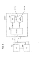
FIG. 1 illustrates an exemplary configuration of a control system 1 and exemplary operations thereof according to a first embodiment. The control system 1 ofFIG. 1 includes anelectronic circuit 11, abus interface 12, asignal maintaining circuit 13, areset control circuit 14, and a control device. The control system 1 ofFIG. 1 includes twocontrol devices - The
electronic circuit 11 is a circuit to be controlled by thecontrol devices control devices electronic circuit 11 by transmitting a control signal via a bus 31. In the present embodiment, one of thecontrol devices - The bus 31 is a serial bus such as an I2C bus. The bus 31 is connected to the
bus interface 12. Thebus interface 12 receives a control signal transmitted from the active control device via the bus 31, and outputs a signal corresponding to the received control signal to theelectronic circuit 11. - The
signal maintaining circuit 13 is disposed in a transmission path of the signal that is output from thebus interface 12 to theelectronic circuit 11. Thesignal maintaining circuit 13 maintains, in accordance with an instruction from thereset control circuit 14, the value of the signal to be output from thebus interface 12 to theelectronic circuit 11 at the value at the time of the reception of the instruction from thereset control circuit 14. - The
reset control circuit 14 is configured to, when the bus 31 becomes unusable, cause thesignal maintaining circuit 13 to maintain the value of the output signal to theelectronic circuit 11, and then resets thebus interface 12. When thebus interface 12 is reset, the bus 31 is restored to an operational state. The above operation of thereset control circuit 14 prevents the signal output from thebus interface 12 to theelectronic circuit 11 from being lost due to the resetting of thebus interface 12. This allows theelectronic circuit 11 to continue operations until the bus 31 is restored. - The following describes, step by step, the operations performed in the control system 1 in the case where an active control device is terminated due to the occurrence of a failure and thus the bus 31 becomes unusable.
- In the following example, the
control device 21 operates as an active control device, and thecontrol device 22 operates as a standby control device in the initial state. In the case where the operations of thecontrol device 21 operating as anactive control device 21 are stopped, thestandby control device 22 becomes active and controls theelectronic circuit 11 in place of thecontrol device 21. Thecontrol device 22 and thereset control circuit 14 are connected to each other with areset signal line 32 for instructing resetting of thebus interface 12. - When the
control device 21 operating as an active control device and thebus interface 12 are communicating with each other via the bus 31, if thecontrol device 21 is terminated due to the occurrence of a failure or the like, the bus 31 is prevented from being released. Accordingly, thecontrol device 22 is unable to perform communication via the bus 31, and thus is unable to take over control of theelectronic circuit 11. - When the
control device 22 detects that thecontrol device 21 has been terminated (Step S1), thecontrol device 22 outputs a reset instruction via the reset signal line 32 (Step S2). Upon receiving the reset instruction, thereset control circuit 14 instructs thesignal maintaining circuit 13 to maintain the value of an output signal to the electronic circuit (Step S3). Thesignal maintaining circuit 13 maintains the value of the signal being output from thebus interface 12 to theelectronic circuit 11 at the time of reception of the instruction from thereset control circuit 14 without any change. Since the value of the signal that is input to theelectronic circuit 11 is maintained, theelectronic circuit 11 is able to continue operations in the same controlled state as it was before the termination of thecontrol device 21. - After instructing the
signal maintaining circuit 13 to maintain the output value, thereset control circuit 14 resets the bus interface 12 (Step S4). For instance, thereset control circuit 14 resets thebus interface 12 after a predetermined time period after reception of the reset instruction via thereset signal line 32. - When the
bus interface 12 is reset, the bus 31 is released. Thecontrol device 22 transmits a control signal via the bus 31, and thereby controls theelectronic circuit 11 in place of thecontrol device 21. When thecontrol device 22 starts controlling theelectronic circuit 11, thesignal maintaining circuit 13 is released from a state of maintaining the output value, in accordance with an instruction from thereset control circuit 14, for example. Then, a signal corresponding to the control signal from thecontrol device 22 is transmitted from thebus interface 12 to theelectronic circuit 11. - According to the control system 1 described above, in the case where the bus 31 becomes unusable due to the termination of the operations of the
control device 22, the bus 31 may be restored by resetting thebus interface 12 while keeping theelectronic circuit 11 operating. Further, thecontrol device 22 may take over control of theelectronic circuit 11 from thecontrol device 21 while keeping theelectronic circuit 11 operating. -
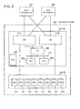
FIG. 2 illustrates an exemplary entire configuration of astorage system 100 according to a second embodiment. Thestorage system 100 includes a controller enclosure (CE) 110 and a drive enclosure (DE) 120. - The
controller enclosure 110 includes controller modules (CMs) 111a and 111b, a front-end router (FRT) 200, service controllers (SCs) 300a and 300b, and a power supply unit (PSU) 400. - Each of the
controller modules controller modules apparatuses - Each of the
controller modules drive enclosure 120 in response to an In/Out (I/O) request from thehost apparatuses controller modules drive enclosure 120, using Redundant Arrays of Inexpensive Disks (RAID), and control access to these physical storage areas, for example. Further, when controlling access to the storage devices of thedrive enclosure 120 in response to an I/O request from thehost apparatuses controller modules drive enclosure 120 into memories of thecontroller modules - The front-
end router 200 is connected to thecontroller modules bus 112. The front-end router 200 includes a PCIe switch and is configured to relay data that is exchanged between thecontroller modules 111a and thecontroller module 111b via thePCIe bus 112. - The
controller modules end router 200. For example, thecontroller module 111a loads the cached data, which has been cached from the storage device of thedrive enclosure 120 into a memory of thecontroller module 111a, into a memory of theother controller module 111b, and thereby duplicates the cached data. In this case, if thecontroller module 111a is terminated due to the occurrence of a failure, thecontroller module 111b may take over, using the duplicated cached data in the memory of thecontroller module 111b, the operation of controlling access to thedrive enclosure 120 which has been performed by thecontroller module 111a. - The front-
end router 200 is connected to theservice controllers service controllers end router 200, and monitor the operations of the PCIe switch. Theservice controllers end router 200 realize a control system for controlling the PCIe switch of the front-end router 200. - The
service controllers end router 200 for the I2C bus 113 operates as a slave device in the I2C bus 113. Theservice controllers service controllers service controller 300a operates as an active service controller, and theservice controller 300b operates as a standby service controller in the initial state. - The
service controller 300b operating as a standby service controller monitors whether theservice controller 300a is operating normally. If theservice controller 300b detects that theservice controller 300a has been abnormally terminated, theservice controller 300b starts operating as an active service controller so as to take over the operation of controlling the operations of the PCIe switch of the front-end router 200 and the operation of monitoring the PCIe switch. - The
power supply unit 400 converts an externally supplied alternating current (AC) supply voltage into a direct current (DC) voltage, and supplies the DC voltage to the components of thecontroller enclosure 110. - The
drive enclosure 120 includes a plurality of storage devices to be accessed by thecontroller modules drive enclosure 120 of this embodiment is a disk array apparatus including hard disk drives (HDDs) or solid state drives (SSDs) as storage devices. -
FIG. 3 illustrates an exemplary hardware configuration of theservice controller 300a. It is to be noted that both theservice controllers service controller 300a. - The entire operation of the
service controller 300a is controlled by aCPU 301. A random access memory (RAM) 302 and a plurality of peripheral devices are connected to theCPU 301 through abus 307. TheRAM 302 is used as a primary storage device of theservice controller 300a. TheRAM 302 temporarily stores at least part of a firmware program to be executed by theCPU 301, and various types of data used for processing to be performed by this firmware program. - As examples of peripheral devices, a
non-volatile memory 303, abus interface 304, areset output circuit 305, and amonitoring circuit 306 are connected to theCPU 301. - The
non-volatile memory 303 is used as a secondary storage device of theservice controller 300a, and is configured to store the firmware program to be executed by the CPU 3011, various types of data used for execution of the firmware program, and the like. - The
bus interface 304 performs interface processing for exchanging data via the I2C bus 113. The I2C bus 113 includes a data signal line and a clock signal line. Thebus interface 304 transmits control data via the data signal line and receives response data transmitted from the slave device (the bus interface of the front-end router 200) via the data signal line, under the control of theCPU 301. Further, thebus interface 304 outputs a clock signal to the clock signal line when sending the control data and when receiving the response data. - Further, a
reset signal line 114 for instructing resetting of the bus interface is connected to theservice controller 300a. Thereset output circuit 305 outputs a reset instruction signal to thereset signal line 114 in accordance with an instruction from theCPU 301. - The
service controller 300a and theservice controller 300b are connected to each other through amonitoring signal line 115 for monitoring each other. Themonitoring circuit 306 exchanges monitoring signals with a monitoring circuit of theother service controller 300b via themonitoring signal line 115. For example, the CPU of a service controller operating as an active service controller causes a monitoring circuit of the active service controller to transmit a monitoring signal at a constant frequency to the other service controller operating as a standby service controller. The monitoring circuit of the standby service controller having received the monitoring signal from the active service controller notifies the CPU of the standby service controller of the reception of the monitoring signal. If the monitoring circuit of the standby service controller does not receive a monitoring signal for a certain period of time or longer, the CPU of the standby service controller determines that the active service controller is abnormally terminated. -
FIG. 4 illustrates an exemplary hardware configuration of the front-end router 200. The front-end router 200 includes aPCIe switch 210, a DC/DC converter (DDC) 220, an I2C-GPIO (General Purpose Input/Output) 230, asignal maintaining circuit 240, and areset control circuit 250. - The
PCIe switch 210 is configured to relay data that are exchanged between thecontroller modules 111a and thecontroller module 111b via thePCIe bus 112. Further, thePCIe switch 210 may exchange signals with the I2C-GPIO 230. ThePCIe switch 210 executes an operation corresponding to a control signal from the I2C-GPIO 230, and returns information requested by the I2C-GPIO 230. For example, thePCIe switch 210 resets itself in accordance with a reset instruction from the I2C-GPIO 230. Also, thePCIe switch 210 returns information indicating the state of thePCIe switch 210, such as temperature information and drive voltage information, in response to a request from the I2C-GPIO 230. - The DC/
DC converter 220 converts a DC voltage from thepower supply unit 400 into a predetermined voltage, and supplies the predetermined voltage to thePCIe switch 210 as a drive voltage. Further, the on and off of the DC/DC converter 220 is controlled in accordance with a control signal (a power-on signal described below) that is output from the I2C-GPIO 230. - The I2C-
GPIO 230 is a bus interface circuit for the I2C bus 113. The I2C-GPIO 230 operates as a slave circuit on the I2C bus 113, and is configured to receive a control signal from one of theservice controllers - Further, the I2C-
GPIO 230 having received control signal from one of theservice controllers end router 200, and transmits the converted control signal to thePCIe switch 210 or the DC/DC converter 220. For example, if the I2C-GPIO 230 receives an instruction for turning off the DC/DC converter 220 via the I2C bus 113, the I2C-GPIO 230 switches the power-on signal to be transmitted to the DC/DC converter 220 from high level to low level. - Also, the I2C-
GPIO 230 may load a signal transmitted to thePCIe switch 210 and the DC/DC converter 220 from thesignal maintaining circuit 240 in accordance with an instruction from any one of theservice controllers - Further, the I2C-
GPIO 230 is reset when a reset signal output from thereset control circuit 250 is switched from low level to high level. As will be described below, in the case where the service controller communicating with the I2C-GPIO 230 is abnormally terminated or in the case where the I2C-GPIO 230 is abnormally terminated, communication via the I2C bus 113 is disabled. Then, if the I2C-GPIO 230 is reset, the I2C bus 113 is restored. This enables communication between the I2C-GPIO 230 and one of theservice controllers - The
signal maintaining circuit 240 is disposed in a transmission path of a signal that is transmitted from the I2C-GPIO 230 to thePCIe switch 210 and the DC/DC converter 220. Thesignal maintaining circuit 240 maintains the values of the signals to be transmitted from the I2C-GPIO 230 to thePCIe switch 210 and the DC/DC converter 220 at the values at the time of the reception of an instruction from thereset control circuit 250. - The
reset control circuit 250 is connected to theservice controllers reset signal line 114. When thereset control circuit 250 receives an instruction for resetting the I2C-GPIO 230 via thereset signal line 114, thereset control circuit 250 causes thesignal maintaining circuit 240 to maintain the values of the output signals, and delays the timing of resetting the I2C-GPIO 230. With this operation, thereset control circuit 250 prevents the operations of thePCIe switch 210 from being stopped before completion of the reset operation of the I2C-GPIO 230 due to loss of the signals to thePCIe switch 210 and the DC/DC converter 220 from the I2C-GPIO 230. -
FIG. 5 illustrates a reference example of a front-end router. A description will be given of the problem which may occur in the case where an I2C bus 113 becomes unusable with reference toFIG. 5 . InFIG. 5 , elements corresponding to those ofFIG. 4 are denoted by the same reference numerals. - A front-
end router 500 illustrated inFIG. 5 is an example in which thesignal maintaining circuit 240 and thereset control circuit 250 of the front-end router 200 are not provided. That is, output signals from an I2C-GPIO 230a are transmitted to aPCIe switch 210 and a DC/DC converter 220 without passing through thesignal maintaining circuit 240. The I2C-GPIO 230a is different from the I2C-GPIO 230 ofFIG. 4 in not having a function of loading an output signal from thesignal maintaining circuit 240. Further, the I2C-GPIO 230a is directly connected to areset signal line 114, and is reset in accordance with an instruction transmitted via thereset signal line 114. - In
FIG. 5 , a reset signal RST for instructing resetting is illustrated as an example of a control signal that is output from the I2C-GPIO 230a to thePCIe switch 210. For example, thePCIe switch 210 is reset when the reset signal RST is switched from high level to low level. - Further, in
FIG. 5 , a power-on signal Pon for controlling an operation of supplying a drive voltage to thePCIe switch 210 is illustrated as an example of a control signal that is output from the I2C-GPIO 230a to the DC/DC converter 220. For example, the DC/DC converter 220 supplies a drive voltage to thePCIe switch 210 when the power-on signal Pon is high level, and stops supplying the drive voltage to thePCIe switch 210 when the power-on signal Pon is low level. - The following describes operations in the case where the
service controllers end router 500. In the following description, it is assumed that theservice controller 300a having been operating as an active service controller is abnormally terminated. When theservice controller 300b operating as a standby service controller detects that theservice controller 300a has been abnormally terminated, theservice controller 300b attempts to become active so as to take over the operation of controlling the operations of thePCIe switch 210 of the front-end router 500 and the operation of monitoring thePCIe switch 210. However, since theservice controller 300a has been terminated, the I2C bus 113 is prevented from being released. Thus, theservice controller 300b is not able to perform communication via the I2C bus 113. - For example, when the
service controller 300a operating as a master device on the I2C bus 113 is terminated, transmission of a clock signal to a clock signal line of the I2C bus 113 is stopped. If transmission of a clock signal is stopped when the I2C-GPIO 230a operating as a slave device is transmitting data, the data transmission operation by the I2C-GPIO 230a is stopped. Then, the potential of a data signal line is fixed to either high level or low level. Thus, the I2C bus 113 becomes unusable, theservice controller 300b having become active is not able to perform communication via the I2C bus 113. - Then, the
service controller 300b instructs resetting of the I2C-GPIO 230a via thereset signal line 114. When the I2C-GPIO 230a is reset, the I2C bus 113 is restored. However, when the I2C-GPIO 230a is reset, output signals from the I2C-GPIO 230a to thePCIe switch 210 and the DC/DC converter 220 are lost. Therefore, even if there is no failure in thePCIe switch 210, thePCIe switch 210 becomes unable to continue the last operation. - For instance, if the reset signal RST becomes low level due to resetting of the I2C-
GPIO 230a, thePCIe switch 210 is also reset. Further, if the power-on signal Pon becomes low level due to resetting of the I2C-GPIO 230a, supply of a drive voltage to thePCIe switch 210 is stopped. In both cases, the operations of thePCIe switch 210 are stopped. When thePCIe switch 210 is terminated, thecontroller module 111a and thecontroller module 111b become unable to communicate with each other, and thus become unable to duplicate of cached data, for example. This affects operations of thestorage system 100. - In order to overcome the above problem, in the front-
end router 200 ofFIG. 4 of this embodiment, when a reset instruction is issued from theservice controller 300b, thereset control circuit 250 causes thesignal maintaining circuit 240 to maintain the values of the output signals to thePCIe switch 210 and the DC/DC converter 220 before resetting the I2C-GPIO 230. This prevents the output signals to thePCIe switch 210 and the DC/DC converter 220 from being lost due to the resetting of the I2C-GPIO 230, and thereby allows thePCIe switch 210 to continue operations even during the reset process of the I2C-GPIO 230. -
FIG. 6 illustrates an example of a signal transmitted within the front-end router 200. - In the following description, a reset signal RST and a power-on signal Pon are illustrated as examples of control signals output by the I2C-
GPIO 230. The reset signal RST is supplied to thePCIe switch 210 via thesignal maintaining circuit 240, and the power-on signal Pon is supplied to the DC/DC converter 220 via thesignal maintaining circuit 240. ThePCIe switch 210 is reset when the reset signal RST is switched from high level to low level. The DC/DC converter 220 supplies a drive voltage to thePCIe switch 210 when the power-on signal Pon is high level, and stops supplying the drive voltage to thePCIe switch 210 when the power-on signal Pon is low level. - The
signal maintaining circuit 240 outputs control signals (in this example, the reset signal RST and the power-on signal Pon) that are output from the I2C-GPIO 230 without any change when an enable signal EN2 is high level. When the enable signal EN2 is low level, thesignal maintaining circuit 240 maintains the values of the control signals that had been output from the I2C-GPIO 230 at the time the enable signal EN2 was switched to low level, until the enable signal EN2 becomes high level. - The I2C-
GPIO 230 is reset when a reset signal I2C-RST2 from thereset control circuit 250 is switched from low level to high level. Further, when the I2C-GPIO 230 receives an instruction from the service controller via the I2C bus 113, the I2C-GPIO 230 switches an enable signal EN1 to be output to thereset control circuit 250 to low level or high level. When the I2C-GPIO 230 is operating normally, the enable signal EN1 is high level. Also, the I2C-GPIO 230 loads the control signals (in this example, the reset signal RST and the power-on signal Pon) being output from thesignal maintaining circuit 240, and outputs control signals corresponding to the values of the loaded signals. - The
reset control circuit 250 receives a reset signal I2C-RST1 via thereset signal line 114. Thereset control circuit 250 delays the input value of the reset signal I2C-RST1 by a predetermined time, and outputs the delayed reset signal I2C-RST1 as a reset signal I2C-RST2 to the I2C-GPIO 230. - Further, when the reset signal I2C-RST1 is switched from low level to high level, the
reset control circuit 250 switches the enable signal EN2 from high level to low level and causes thesignal maintaining circuit 240 to maintain the output value. After that, when the enable signal EN1 from the I2C-GPIO 230 having been reset is switched from low level to high level, thereset control circuit 250 switches the enable signal EN2 to high level. -
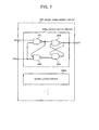
FIG. 7 illustrates an exemplary internal configuration of thesignal maintaining circuit 240. Thesignal maintaining circuit 240 includes the same number ofgated latch circuits - The
gated latch circuit 240a includes four NAND (negative AND)gates 241 through 244. TheNAND gate 241 has one input terminal IN to which the control signal from the I2C-GPIO 230 is input and the other input terminal to which the enable signal EN2 from thereset control circuit 250 is input. TheNAND gate 242 has one input terminal to which an output signal from theNAND gate 241 is input and the other input terminal to which the enable signal EN2 from thereset control circuit 250 is input. TheNAND gate 243 has one input terminal to which the output signal from theNAND gate 241 is input and the other input terminal to which an output signal from theNAND gate 244 is input. TheNAND gate 244 has one input terminal to which an output signal from theNAND gate 243 is input and the other input terminal to which an output signal from theNAND gate 242 is input. The output signal from theNAND gate 243 is output from an output terminal OUT. - In the
gated latch circuit 240a having the configuration described above, when the enable signal EN2 is high level, the output value from the out terminal OUT is the same as the value of the control signal input to the input terminal IN. On the other hand, when the enable signal EN2 is low level, the output value from the output terminal OUT is maintained at the value of the control signal input to the input terminal IN at the time the enable signal EN2 was switched to low level. - It is to be noted that a common enable signal EN2 is input to each of the
gated latch circuits signal maintaining circuit 240. It is noted that the gated latch circuit may have any other circuit configuration. -
FIG. 8 illustrates an exemplary internal configuration of thereset control circuit 250. Thereset control circuit 250 includes an AND (logical AND)gate 251 and a flip-flop (FF) 252. - The AND
gate 251 has one input terminal to which the enable signal EN1 from the I2C-GPIO 230 is input and the other input terminal to which an inverted signal of the reset signal I2C-RST1 is input. An output signal from the ANDgate 251 is output as an enable signal EN2 to thesignal maintaining circuit 240. - This AND
gate 251 changes the level of the enable signal EN2 as follows. If the enable signal EN1 is high level and the reset signal I2C-RST1 is low level, the enable signal EN2 becomes high level. If the enable signal EN1 is low level or if the reset signal I2C-RST1 is low level, the enable signal EN2 becomes low level. Similarly, if both of these conditions are satisfied, the enable signal EN2 becomes low level. It is to be noted that the circuit configuration of thereset control circuit 250 is not limited to that ofFIG. 8 as long as the enable signal EN1, the reset signal I2C-RST1, and the enable signal EN2 interlock each other as described above. - The flip-
flop 252 has a data input terminal to which the reset signal I2C-RST1 is input via thereset signal line 114, and has a clock input terminal to which a clock signal CLK is input. The clock signal CLK is generated in thecontroller enclosure 110, for example. The flip-flop 252 delays the reset signal I2C-RST1 by a time period corresponding to the period of the clock signal CLK, and outputs the delayed reset signal I2C-RST1 as a reset signal I2C-RST2 to the I2C-GPIO 230. - It is to be noted that the
reset control circuit 250 may include a plurality of serially connected flip-flops so as to delay the reset signal I2C-RST1 by a predetermined time, for example. Alternatively, thereset control circuit 250 may include other types of delay circuits than the flip-flop as a circuit for delaying the reset signal I2C-RST1. - Next, operations of the
service controllers end router 200 will be described with reference to a sequence diagram and a timing chart. -
FIG. 9 is a sequence diagram illustrating an exemplary process performed in the case where thecontroller enclosure 110 is powered on. - (Step S11) The
controller enclosure 110 is powered on in response to an operation performed on a power switch (not illustrated) of thecontroller enclosure 110. Then, theservice controllers GPIO 230 are activated. Further, a drive voltage is supplied to the DC/DC converter 220, thesignal maintaining circuit 240, and thereset control circuit 250. In the following description, it is assumed that theservice controller 300a operates as an active service controller. - (Step S12) In order to instruct resetting of the I2C-
GPIO 230, theservice controller 300a maintains the reset signal I2C-RST1 at high (H) level for a certain period of time, and then switches the reset signal I2C-RST1 to low (L) level. - (Step S13) After a certain period of time after the reset signal I2C-RST1 was switched to high level, the
reset control circuit 250 switches the reset signal I2C-RST2 to high level. Thus, the I2C-GPIO 230 is reset. Further, after a certain period of time after the reset signal I2C-RST1 was switched to low level, thereset control circuit 250 switches the reset signal I2C-RST2 to low level.
It is to be noted that the operations in Steps S12 and S13 do not have to be performed as long as the I2C-GPIO 230 is successfully activated and both the reset signals I2C-RST1 and I2C-RST2 are low level at the time of starting Step S14. - (Step S14) The
service controller 300a instructs the I2C-GPIO 230 to switch the enable signal EN1 to high level via the I2C bus 113. - (Step S15) The I2C-
GPIO 230 switches the enable signal EN1 to high level in accordance with the instruction from theservice controller 300a. - (Step S16) In response to the enable signal EN1 being switched to high level, the
reset control circuit 250 switches the enable signal EN2 to high level. - (Step S17) In response to the enable signal EN2 being switched to high level, the
signal maintaining circuit 240 is put in a state of outputting the control signals (the reset signal RST and the power-on signal Pon) from the I2C-GPIO 230 without any change. Thus, theservice controller 300a becomes able to control the operations of thePCIe switch 210 and the DC/DC converter 220. - (Step S18) The
service controller 300a instructs the I2C-GPIO 230 to power on and reset thePCIe switch 210 via the I2C bus 113. - (Step S19) The I2C-
GPIO 230 switches the power-on signal Pon to high level in accordance with the instruction from theservice controller 300a. Thus, the DC/DC converter 220 starts supplying a drive voltage to thePCIe switch 210. Further, the I2C-GPIO 230 maintains the reset signal RST at low level for a certain period of time, and then switches the reset signal RST to high level. Thus, thePCIe switch 210 is reset. - (Step S20) The
service controller 300a starts an operation of controlling and monitoring thePCIe switch 210 and the DC/DC converter 220, which is performed by transmitting control signals via the I2C bus 113. For example, theservice controller 300a loads state information indicating the states of thePCIe switch 210 and the DC/DC converter 220, which are circuits to be controlled and monitored, from thePCIe switch 210. The state information may include temperature information and drive voltage information. Then, if theservice controller 300a determines that a failure has occurred in the circuit to be controlled and monitored, theservice controller 300a performs a control operation of resetting the failed circuit or stopping the operations of the failed circuit, for example. -
FIG. 10 is a timing chart illustrating an exemplary transition of the values of signals in the case where the controller enclosure is powered on. - With the operation in Step S12 of
FIG. 9 , the reset signal I2C-RST1 that is input to thereset control circuit 250 is maintained at high level during a period from a timing T11 to a timing T13. At a timing T12 after a certain period of time after the timing T11 at which the reset signal I2C-RST1 was switched to high level, the reset signal I2C-RST2 that is output from thereset control circuit 250 is switched to high level. Then, at a timing T14 after a certain period of time after the timing T13 at which the reset signal I2C-RST1 was switched to low level, the reset signal I2C-RST2 is switched to low level. - The I2C-
GPIO 230 is reset at the timing T12 at which the reset signal I2C-RST2 is switched to high level. The I2C-GPIO 230 maintains the output values of the control signals at their predetermined initial values while the signal I2C-RST2 is high level, for example. - At a timing T15 after the I2C-
GPIO 230 was reset, the I2C-GPIO 230 switches the enable signal EN1 to high level in accordance with an instruction from theservice controller 300a. In response to the reset signal I2C-RST1 being low level and the enable signal EN1 being high level, thereset control circuit 250 switches the enable signal EN2 to high level. Thus, thesignal maintaining circuit 240 is put in a state of outputting the control signals from the I2C-GPIO 230 without any change. It is to be noted that thesignal maintaining circuit 240 maintains the output values of the control signals at predetermined initial values during a period from the power-on to the timing T15. - The above operations performed at the timing T15 correspond to the operations in Steps S13 through S17 of
FIG. 9 . After that, in accordance with an instruction of theservice controller 300a, thePCIe switch 210 starts operating, and theservice controller 300a monitors the operations of thePCIe switch 210. -
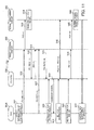
FIG. 11 is a sequence diagram illustrating an exemplary process performed in the case where theactive service controller 300a is abnormally terminated. - (Step S31) The
service controller 300b operating as a standby controller detects that theservice controller 300a has been abnormally terminated, and starts operating as an active service controller. At this point, the I2C bus 113 is unusable. - (Step S32) In order to instruct resetting of the I2C-
GPIO 230, theservice controller 300b switches the reset signal I2C-RST1 to high level. - (Step S33) In response to the reset signal I2C-RST1 being switched to high level, the
reset control circuit 250 switches the enable signal EN2 to low level. - (Step S34) The
signal maintaining circuit 240 maintains the control signals (the reset signal RST and the power-on signal Pon) to be output at the values that has been input from the I2C-GPIO 230 at the time the enable signal EN2 is switched to the low level. In this embodiment, thesignal maintaining circuit 240 maintains both the reset signal RST and the power-on signal Pon at high level. - (Step S35) After a certain period of time after the reset signal I2C-RST1 was switched to high level in Step S32, the
reset control circuit 250 switches the reset signal I2C-RST2 to high level. Thus, the I2C-GPIO 230 is reset, and the I2C bus 113 is restored. - (Step S36) The I2C-
GPIO 230a having been reset sets the value of the enable signal EN1 to low level, which is the initial value thereof. - (Step S37) The
service controller 300b switches the reset signal I2C-RST1 to low level. - (Step S38) After a certain period of time after the reset signal I2C-RST1 was switched to low level, the
reset control circuit 250 switches the reset signal I2C-RST2 to low level. - (Step S39) The
service controller 300b instructs, via the I2C bus 113, the I2C-GPIO 230 to load the values of the control signals being fed back from thesignal maintaining circuit 240 and to report the values. - (Step S40) In accordance with the instruction from the
service controller 300b, the I2C-GPIO 230 loads the values of the control signals being fed back from thesignal maintaining circuit 240. The values of the feedback signals loaded in this step are the values of the outputs that have been maintained by thesignal maintaining circuit 240 from Step S34. That is, the values loaded in this step are the values that were output from the I2C-GPIO 230 at the time immediately before the termination of theservice controller 300a. In this embodiment, the I2C-GPIO 230 loads "1" indicating high level as the value of the reset signal RST, and "1" indicating high level as the value of the power-on signal Pon. The I2C-GPIO 230 reports the loaded values of the feedback signals to theservice controller 300b via the I2C bus 113. - It is to be noted that since the values of the control signals being output from the
signal maintaining circuit 240 are fed back to the I2C-GPIO 230, the I2C-GPIO 230 may easily and reliably recognize the values of the control signals that the I2C-GPIO 230 was outputting before being reset. - (Step S41) The
service controller 300b transmits the reported values of the feedback signals to the I2C-GPIO 230 via the I2C bus 113, and instructs the I2C-GPIO 230 to set again the transmitted values as the values of corresponding control signals. - (Step S42) In accordance with the instruction from the
service controller 300b, the I2C-GPIO 230 sets the output values of both the reset signal RST and the power-on signal Pon to high level. - (Step S43) The
service controller 300b instructs the I2C-GPIO 230 to switch the enable signal EN1 to high level via the I2C bus 113. The purpose of this operation is to return the states of the control signals transmitted from the I2C-GPIO 230 to thePCIe switch 210 and the DC/DC converter 220 via thesignal maintaining circuit 240 to the state at the time immediately before the termination of theservice controller 300a. - (Step S44) The I2C-
GPIO 230 switches the enable signal EN1 to high level in accordance with the instruction from theservice controller 300b. - (Step S45) In response to the enable signal EN1 being switched to the high level, the
reset control circuit 250 switches the enable signal EN2 to high level. - (Step S46) In response to the enable signal EN2 being switched to high level, the
signal maintaining circuit 240 terminates the operation of maintaining the output signals, and outputs the values of the control signals being output from the I2C-GPIO 230 without any change. At this point, the reset signal RST and the power-on signal Pon that are output from thesignal maintaining circuit 240 become the same level, i.e., high level, as those at the time before the enable signal EN2 was switched to high level. - Since the
reset control circuit 250 is configured to recognize, in response to the enable signal EN1 from the I2C-GPIO 230 being switched to high level, the timing of causing thesignal maintaining circuit 240 to terminate the operation of maintaining the output signals, thereset control circuit 250 may recognize this timing even when thereset control circuit 250 is not connected to the I2C bus 113. Accordingly, the configuration of thereset control circuit 250 may be simplified. - It is to be noted that, after the output values of the reset signal RST and the power-on signal Pon are both set to high level in Step S42, the I2C-
GPIO 230 may autonomously switch the enable signal EN1 to high level without receiving an instruction from theservice controller 300b, for example. - With the operations up to Step S46, during a period from the termination of the
service controller 300b to Step S46, both the reset signal RST and the power-on signal Pon that are output from thesignal maintaining circuit 240 are maintained at high level. Therefore, the termination of theservice controller 300b and the operation of resetting the I2C-GPIO 230 for releasing the I2C bus 113 do not affect the signal relay operation of thePCIe switch 210. This allows thePCIe switch 210 to continue the signal relay operation, and also allows thecontroller modules - (Step S47) The
service controller 300b starts an operation of controlling and monitoring thePCIe switch 210 and the DC/DC converter 220 by transmitting control signals via the I2C bus 113. That is, theservice controller 300b takes over the control and monitoring operation that has been performed by theservice controller 300a. - It is to be noted that, in the operations of
FIG. 11 described above, the I2C-GPTO 230 loads the values of the feedback signals from thesignal maintaining circuit 240 and reports the loaded values to theservice controller 300b in accordance with an instruction from theservice controller 300b (Steps S39 and S40), and then sets the values reported from theservice controller 300b as the output values of the control signals (Steps S41, and S42). However, after loading the feedback signals, the I2C-GPIO 230 may set the loaded values as the output values of the control signals without waiting for an instruction from theservice controller 300b, for example. - Further, in an alternative configuration, the I2C-
GPIO 230 does not have a function of loading the values of the feedback signals from thesignal maintaining circuit 240. In this case, thestandby service controller 300b monitors control signals transmitted from theactive service controller 300a to the I2C-GPIO 230, and records the history of these control signals in the RAM. When theservice controller 300b detects that theservice controller 300a has been terminated, theservice controller 300b analyzes the history recorded in the RAM, and determines the last values of the reset signal RST and the power-on signal Pon output from the I2C-GPIO 230. Theservice controller 300b transmits a control signal that sets the reset signal RST and the power-on signal Pon to the determined last values to the I2C-GPIO 230 via the I2C bus 113. Thus, it is possible to match the values of the reset signal RST and the power-on signal Pon that are output from thesignal maintaining circuit 240 and the values of the reset signal RST and the power-on signal Pon that are output from the I2C-GPIO 230, immediately before the operation of maintaining the output signals in thesignal maintaining circuit 240 is cancelled in Step S46. -
FIG. 12 is a timing chart illustrating an exemplary transition of the values of signals in the case where the active service controller is abnormally terminated. - With the operation in Step S32 of
FIG. 11 , the reset signal I2C-RST1 that is input to thereset control circuit 250 becomes high level at a timing T21. In response to the reset signal I2C-RST1 being switched to high level, thereset control circuit 250 switches the enable signal EN2 to low level. Thesignal maintaining circuit 240 maintains the value of each of the reset signal RST and the power-on signal Pon at the value (high level) that has been input from the I2C-GPIO 230 at the timing T21. - Further, at a timing T22 after a predetermined time period after the reset signal I2C-RST1 was switched to high level, the
reset control circuit 250 switches the reset signal I2C-RST2 to high level. Thus, the I2C-GPIO 230 is reset, and the I2C bus 113 is restored. The I2C-GPIO 230a having been reset sets the value of the enable signal EN1 to low level, and sets the output values of the control signals to their predetermined initial values. - With the operation in Step S37 of
FIG. 11 , the reset signal I2C-RST1 that is input to thereset control circuit 250 becomes low level at a timing T23. At a timing T24 after a predetermined time period after the reset signal I2C-RST1 was switched to low level, thereset control circuit 250 switches the reset signal I2C-RST2 to low level. The I2C-GPIO 230 is switched from the state of setting the output values of the control signals to their initial values to the state of outputting control signals corresponding to the instruction from theservice controller 300b. - With the operations in Steps S39 through S41 of
FIG. 11 , at a timing T25, the I2C-GPIO 230 switches the values of the reset signal RST and the power-on signal Pon to be output to the values that had been output before the I2C-GPIO 230 was reset. Subsequently, at a timing T26, the I2C-GPIO 230 switches the enable signal EN1 to high level in accordance with the instruction from theservice controller 300b. In response to the reset signal I2C-RST1 being low level and the enable signal EN1 being high level, thereset control circuit 250 switches the enable signal EN2 to high level. Thus, thesignal maintaining circuit 240 terminates the operation of maintaining the output signals, and outputs the values of the control signals being output from the I2C-GPIO 230 without any change. At this point, the values of the reset signal RST and the power-on signal Pon that are output from thesignal maintaining circuit 240 become high level, i.e., the same level as those at the time before the enable signal EN2 was switched to high level. - Subsequently, at a timing T27, the
service controller 300b starts a monitoring operation of thePCIe switch 210, which is performed by transmitting a control signal via the I2C bus 113. The I2C-GPIO 230 outputs a control signal corresponding to an instruction from theservice controller 300b, and thesignal maintaining circuit 240 outputs the control signal output from the I2C-GPIO 230 without any change. - In the second embodiment described above, when the I2C bus 113 becomes unusable due to an abnormal termination of the
service controller 300a, the values of control signals being output to thePCIe switch 210 and the DC/DC converter 220 are maintained by thesignal maintaining circuit 240 in accordance with a reset instruction from theservice controller 300b. Then, while the output values of the control signals are maintained by thesignal maintaining circuit 240, the I2C-GPIO 230 is reset, and thus the I2C bus 113 is restored. Accordingly, thePCIe switch 210 may normally continue the operation of relaying signals between thecontroller module 111a and thecontroller module 111b even during a process of restoring the I2C bus 113. - Further, after the I2C bus 113 is restored, the I2C-
GPIO 230 is controlled so as to output control signals having the same values as those before the resetting of the I2C-GPIO 230. Therefore, it is possible to restore the operational states of the I2C-GPIO 230 and thesignal maintaining circuit 240 to the states before the termination of theservice controller 300a. Thus, theservice controller 300b having become active may take over the operation of controlling and monitoring thePCIe switch 210. - In one embodiment, an electronic circuit to be controlled may continue operations even during a process of restoring a bus.
Claims (15)
- A control system comprising:an electronic circuit (11, 210);a bus interface (12, 230) configured to receive, via a bus (31, 113), a control signal for controlling the electronic circuit, and output a signal corresponding to the received control signal to the electronic circuit;a signal maintaining circuit (13, 240) configured to maintain a value of the signal to be output from the bus interface to the electronic circuit;a reset control circuit (14, 250) configured to cause the signal maintaining circuit to maintain the value of the output signal to the electronic circuit, and subsequently reset the bus interface; anda control device (21, 22, 300a, 300b) configured to control the electronic circuit by outputting the control signal via the bus.
- The control system according to claim 1, wherein the control device includes
a first control device (21, 300a); and
a second control device (22, 300b) configured to, upon detecting that operations of the first control device have been terminated, output a reset instruction via a reset signal line, and subsequently control the electronic circuit in place of the first control device; and
wherein the reset control circuit is configured to, upon receiving the reset instruction via the reset signal line (S32), cause the signal maintaining circuit to maintain the value of the output signal to the electronic circuit (S33), and subsequently reset the bus interface (S35). - The control system according to claim 2, wherein the bus interface is configured to, after being reset by the reset control circuit (S35), output again to the signal maintaining circuit a value of a signal being output from the signal maintaining circuit to the electronic circuit, in accordance with an instruction from the second control device via the bus (S42).
- The control system according to claim 3, wherein the bus interface is configured to output again to the signal maintaining circuit the value of the signal being output from the signal maintaining circuit to the electronic circuit, by loading the value of the signal being output from the signal maintaining circuit to the electronic circuit (S40) and outputting the loaded value of the signal to the signal maintaining circuit.
- The control system according to claim 3 or 4, wherein after the bus interface has output again to the signal maintaining circuit the value of the signal being output from the signal maintaining circuit to the electronic circuit, the reset control circuit releases the signal maintaining circuit from a state of maintaining the value of the output signal to the electronic circuit (S45).
- The control system according to claim 5,
wherein the second control device is configured to instruct the bus interface via the bus to output again to the signal maintaining circuit the value of the signal being output from the signal maintaining circuit to the electronic circuit (S41), and subsequently transmit to the bus interface via the bus a release instruction for releasing the signal maintaining circuit from the state of maintaining the value of the output signal (S43); and
wherein the reset control circuit is configured to, in response to reception of the release instruction by the bus interface, release the signal maintaining circuit from the state of maintaining the value of the output signal to the electronic circuit (S45). - The control system according to any one of claims 1 to 6, wherein the signal maintaining circuit is configured to maintain, as the signal to be output from the bus interface to the electronic circuit, a value of a signal (RST) for instructing the electronic circuit to perform resetting.
- The control system according to any one of claims 1 to 7, wherein the signal maintaining circuit is configured to maintain, as the signal to be output from the bus interface to the electronic circuit, a value of a signal (Pon) for instructing on and off of power supply to the electronic circuit.
- A relay apparatus comprising:a relay circuit (210) configured to relay signals transmitted and received between a plurality of information processing apparatuses (111a, 111b);a bus interface (230) configured to receive, via a bus, a control signal for controlling the relay circuit, and output a signal corresponding to the received control signal to the relay circuit;a signal maintaining circuit (240) configured to maintain a value of the signal to be output from the bus interface to the relay circuit; anda reset control circuit (250) configured to cause the signal maintaining circuit to maintain the value of the output signal to the relay circuit, and subsequently reset the bus interface.
- The relay apparatus according to claim 9, wherein the reset control circuit is configured to, upon
receiving a reset instruction via a reset signal line from a control device connected to the bus (S32), cause the signal maintaining circuit to maintain the value of the output signal to the relay circuit (S33), and subsequently reset the bus interface. (S35). - The relay apparatus according to claim 10, wherein the bus interface is configured to, after being reset by the reset control circuit, output again to the signal maintaining circuit a value of a signal being output from the signal maintaining circuit to the relay circuit, in accordance with an instruction from the control device via the bus.
- The relay apparatus according to claim 11, wherein the bus interface is configured to output again to the signal maintaining circuit the value of the signal being output from the signal maintaining circuit to the relay circuit, by loading the value of the signal being output from the signal maintaining circuit to the relay circuit and outputting the loaded value of the signal to the signal maintaining circuit.
- The relay apparatus according to claim 11 or 12, wherein after the bus interface has output again to the signal maintaining circuit the value of the signal being output from the signal maintaining circuit to the relay circuit, the reset control circuit releases the signal maintaining circuit from a state of maintaining the value of the output signal to the relay circuit.
- The relay apparatus according to any one of claims 10 to 13 wherein the signal maintaining circuit is configured to maintain, as the signal to be output from the bus interface to the relay circuit, a value of a signal for instructing the relay circuit to perform resetting.
- The relay apparatus according to any one of claims 10 to 14, wherein the signal maintaining circuit is configured to maintain, as the signal to be output from the bus interface to the relay circuit, a value of a signal for instructing on and off of power supply to the relay circuit.
Applications Claiming Priority (1)
| Application Number | Priority Date | Filing Date | Title |
|---|---|---|---|
| JP2011278822A JP5794137B2 (en) | 2011-12-20 | 2011-12-20 | Control system and relay device |
Publications (2)
| Publication Number | Publication Date |
|---|---|
| EP2608049A1 true EP2608049A1 (en) | 2013-06-26 |
| EP2608049B1 EP2608049B1 (en) | 2015-02-25 |
Family
ID=47504596
Family Applications (1)
| Application Number | Title | Priority Date | Filing Date |
|---|---|---|---|
| EP20120192374 Active EP2608049B1 (en) | 2011-12-20 | 2012-11-13 | Control system and relay apparatus |
Country Status (5)
| Country | Link |
|---|---|
| US (1) | US9111052B2 (en) |
| EP (1) | EP2608049B1 (en) |
| JP (1) | JP5794137B2 (en) |
| KR (1) | KR101351194B1 (en) |
| CN (1) | CN103176937A (en) |
Cited By (2)
| Publication number | Priority date | Publication date | Assignee | Title |
|---|---|---|---|---|
| KR101351194B1 (en) | 2011-12-20 | 2014-01-14 | 후지쯔 가부시끼가이샤 | Control system and relay apparatus |
| CN111208892A (en) * | 2020-01-10 | 2020-05-29 | 江苏钜芯集成电路技术股份有限公司 | By serial I2Method for resetting chip system by C signal |
Families Citing this family (7)
| Publication number | Priority date | Publication date | Assignee | Title |
|---|---|---|---|---|
| KR102002888B1 (en) * | 2013-11-05 | 2019-07-23 | 휴렛-팩커드 디벨롭먼트 컴퍼니, 엘.피. | Electronic device and method for checking connected state of signal line thereof |
| CN103645975B (en) * | 2013-11-28 | 2016-06-15 | 华为技术有限公司 | A kind of method of abnormal restoring and serial bus transmission device |
| JP2015153075A (en) * | 2014-02-13 | 2015-08-24 | 富士通株式会社 | Transmission equipment and control unit |
| JP6264155B2 (en) * | 2014-03-31 | 2018-01-24 | 富士通株式会社 | Information processing apparatus, information processing apparatus control method, and information processing apparatus control program |
| CN107957885B (en) * | 2017-12-01 | 2021-02-26 | 麒麟软件有限公司 | PCIE link equipment standby and recovery method based on Feiteng platform |
| CN108040214B (en) * | 2017-12-08 | 2023-09-22 | 延锋伟世通电子科技(南京)有限公司 | Architecture for realizing interconnection of vehicle-mounted entertainment system and instrument double screens through SPI channel in FPD-Link III |
| US11513981B2 (en) * | 2020-04-29 | 2022-11-29 | Dell Products L.P. | PCIe link management without sideband signals |
Citations (6)
| Publication number | Priority date | Publication date | Assignee | Title |
|---|---|---|---|---|
| US6253267B1 (en) * | 1997-07-31 | 2001-06-26 | Samsung Electronics Co., Ltd. | Hot-plug of PCI bus using single chip |
| JP2002063080A (en) | 2000-08-15 | 2002-02-28 | Sony Corp | Interface device |
| JP2004528627A (en) | 2001-02-08 | 2004-09-16 | インターナショナル・ビジネス・マシーンズ・コーポレーション | Computer bus architecture |
| US20070112990A1 (en) * | 2005-11-15 | 2007-05-17 | Matsushita Electric Industrial Co., Ltd. | Iic bus communication system, slave device, and method for controlling iic bus communication |
| US20080177917A1 (en) * | 2007-01-23 | 2008-07-24 | Brian James Cagno | Apparatus, system, and method for automatically resetting an inter-integrated circuit bus |
| JP2010055474A (en) | 2008-08-29 | 2010-03-11 | Internatl Business Mach Corp <Ibm> | Serial bus system and hung slave reset method |
Family Cites Families (8)
| Publication number | Priority date | Publication date | Assignee | Title |
|---|---|---|---|---|
| JP2002202947A (en) | 2000-12-28 | 2002-07-19 | Ricoh Co Ltd | Image processing apparatus, control method thereof, and storage medium storing program |
| US7089338B1 (en) * | 2002-07-17 | 2006-08-08 | Cypress Semiconductor Corp. | Method and apparatus for interrupt signaling in a communication network |
| US7016993B2 (en) * | 2002-12-17 | 2006-03-21 | Inventec Corporation | I2C MUX with anti-lock device |
| US7355438B2 (en) * | 2003-09-26 | 2008-04-08 | Moore Industries-International, Inc. | Electronic circuit |
| US7478286B2 (en) * | 2005-04-08 | 2009-01-13 | Linear Technology Corporation | Circuit and method of detecting and resolving stuck I2C buses |
| US20070240019A1 (en) * | 2005-12-29 | 2007-10-11 | International Business Machines Corporation | Systems and methods for correcting errors in I2C bus communications |
| JP2008250632A (en) * | 2007-03-30 | 2008-10-16 | Matsushita Electric Ind Co Ltd | Data processing system |
| JP5794137B2 (en) | 2011-12-20 | 2015-10-14 | 富士通株式会社 | Control system and relay device |
-
2011
- 2011-12-20 JP JP2011278822A patent/JP5794137B2/en active Active
-
2012
- 2012-11-01 US US13/665,965 patent/US9111052B2/en active Active
- 2012-11-13 EP EP20120192374 patent/EP2608049B1/en active Active
- 2012-11-23 CN CN2012104834183A patent/CN103176937A/en active Pending
- 2012-11-26 KR KR20120134524A patent/KR101351194B1/en not_active Expired - Fee Related
Patent Citations (6)
| Publication number | Priority date | Publication date | Assignee | Title |
|---|---|---|---|---|
| US6253267B1 (en) * | 1997-07-31 | 2001-06-26 | Samsung Electronics Co., Ltd. | Hot-plug of PCI bus using single chip |
| JP2002063080A (en) | 2000-08-15 | 2002-02-28 | Sony Corp | Interface device |
| JP2004528627A (en) | 2001-02-08 | 2004-09-16 | インターナショナル・ビジネス・マシーンズ・コーポレーション | Computer bus architecture |
| US20070112990A1 (en) * | 2005-11-15 | 2007-05-17 | Matsushita Electric Industrial Co., Ltd. | Iic bus communication system, slave device, and method for controlling iic bus communication |
| US20080177917A1 (en) * | 2007-01-23 | 2008-07-24 | Brian James Cagno | Apparatus, system, and method for automatically resetting an inter-integrated circuit bus |
| JP2010055474A (en) | 2008-08-29 | 2010-03-11 | Internatl Business Mach Corp <Ibm> | Serial bus system and hung slave reset method |
Cited By (3)
| Publication number | Priority date | Publication date | Assignee | Title |
|---|---|---|---|---|
| KR101351194B1 (en) | 2011-12-20 | 2014-01-14 | 후지쯔 가부시끼가이샤 | Control system and relay apparatus |
| CN111208892A (en) * | 2020-01-10 | 2020-05-29 | 江苏钜芯集成电路技术股份有限公司 | By serial I2Method for resetting chip system by C signal |
| CN111208892B (en) * | 2020-01-10 | 2022-04-01 | 江苏钜芯集成电路技术股份有限公司 | Method for resetting chip system by using serial I2C signal |
Also Published As
| Publication number | Publication date |
|---|---|
| JP2013130961A (en) | 2013-07-04 |
| CN103176937A (en) | 2013-06-26 |
| KR20130071357A (en) | 2013-06-28 |
| US20130159585A1 (en) | 2013-06-20 |
| KR101351194B1 (en) | 2014-01-14 |
| JP5794137B2 (en) | 2015-10-14 |
| EP2608049B1 (en) | 2015-02-25 |
| US9111052B2 (en) | 2015-08-18 |
Similar Documents
| Publication | Publication Date | Title |
|---|---|---|
| EP2608049B1 (en) | Control system and relay apparatus | |
| US8812913B2 (en) | Method and apparatus for isolating storage devices to facilitate reliable communication | |
| KR101410596B1 (en) | Information processing apparatus, computer program, and copy control method | |
| US7032128B2 (en) | Method for managing computer, apparatus for managing computer, and computer readable medium storing program for managing computer | |
| US20200133759A1 (en) | System and method for managing, resetting and diagnosing failures of a device management bus | |
| US10234929B2 (en) | Storage system and control apparatus | |
| US12282391B2 (en) | Systems and methods for error recovery in rebootless firmware updates | |
| KR20120030311A (en) | Hybrid raid controller having multi pci bus switching | |
| US20240289243A1 (en) | Server and control method therefor | |
| KR100827287B1 (en) | Semiconductor auxiliary memory and data storage method using same | |
| CN115834446A (en) | Dual-control device, control method, storage medium and electronic device | |
| US20160373338A1 (en) | Storage apparatus, control method, and connection device | |
| CN106909307A (en) | A kind of method and device for managing dual-active storage array | |
| KR20120012950A (en) | Hybrid RAID Controller | |
| US9207741B2 (en) | Storage apparatus, controller module, and storage apparatus control method | |
| CN103150224A (en) | Electronic equipment and method for improving starting reliability | |
| JP2008203957A (en) | Nas system | |
| KR101200997B1 (en) | Raid controller having multi pci bus switching | |
| US11294445B2 (en) | Information processing apparatus and method of controlling information processing apparatus | |
| JP5909948B2 (en) | Information processing apparatus and information processing apparatus testing method | |
| JP2009237758A (en) | Server system, server management method, and program therefor | |
| US20200294592A1 (en) | Device and method for backup signal management | |
| KR101317763B1 (en) | Semiconductor storage device-based data restoration | |
| US8862793B2 (en) | Storage system, control device, and storage system control method of controlling storage system | |
| US8499130B2 (en) | Information processing apparatus, information processing method, and recording medium that records history information control program |
Legal Events
| Date | Code | Title | Description |
|---|---|---|---|
| AK | Designated contracting states |
Kind code of ref document: A1 Designated state(s): AL AT BE BG CH CY CZ DE DK EE ES FI FR GB GR HR HU IE IS IT LI LT LU LV MC MK MT NL NO PL PT RO RS SE SI SK SM TR |
|
| AX | Request for extension of the european patent |
Extension state: BA ME |
|
| PUAI | Public reference made under article 153(3) epc to a published international application that has entered the european phase |
Free format text: ORIGINAL CODE: 0009012 |
|
| 17P | Request for examination filed |
Effective date: 20130919 |
|
| RBV | Designated contracting states (corrected) |
Designated state(s): AL AT BE BG CH CY CZ DE DK EE ES FI FR GB GR HR HU IE IS IT LI LT LU LV MC MK MT NL NO PL PT RO RS SE SI SK SM TR |
|
| GRAP | Despatch of communication of intention to grant a patent |
Free format text: ORIGINAL CODE: EPIDOSNIGR1 |
|
| RIC1 | Information provided on ipc code assigned before grant |
Ipc: G06F 13/42 20060101AFI20140827BHEP |
|
| INTG | Intention to grant announced |
Effective date: 20140922 |
|
| GRAS | Grant fee paid |
Free format text: ORIGINAL CODE: EPIDOSNIGR3 |
|
| GRAA | (expected) grant |
Free format text: ORIGINAL CODE: 0009210 |
|
| AK | Designated contracting states |
Kind code of ref document: B1 Designated state(s): AL AT BE BG CH CY CZ DE DK EE ES FI FR GB GR HR HU IE IS IT LI LT LU LV MC MK MT NL NO PL PT RO RS SE SI SK SM TR |
|
| REG | Reference to a national code |
Ref country code: GB Ref legal event code: FG4D |
|
| REG | Reference to a national code |
Ref country code: CH Ref legal event code: EP |
|
| REG | Reference to a national code |
Ref country code: IE Ref legal event code: FG4D |
|
| REG | Reference to a national code |
Ref country code: DE Ref legal event code: R096 Ref document number: 602012005426 Country of ref document: DE Effective date: 20150409 |
|
| REG | Reference to a national code |
Ref country code: AT Ref legal event code: REF Ref document number: 712510 Country of ref document: AT Kind code of ref document: T Effective date: 20150415 |
|
| REG | Reference to a national code |
Ref country code: NL Ref legal event code: VDEP Effective date: 20150225 |
|
| REG | Reference to a national code |
Ref country code: AT Ref legal event code: MK05 Ref document number: 712510 Country of ref document: AT Kind code of ref document: T Effective date: 20150225 |
|
| REG | Reference to a national code |
Ref country code: LT Ref legal event code: MG4D |
|
| PG25 | Lapsed in a contracting state [announced via postgrant information from national office to epo] |
Ref country code: HR Free format text: LAPSE BECAUSE OF FAILURE TO SUBMIT A TRANSLATION OF THE DESCRIPTION OR TO PAY THE FEE WITHIN THE PRESCRIBED TIME-LIMIT Effective date: 20150225 Ref country code: NO Free format text: LAPSE BECAUSE OF FAILURE TO SUBMIT A TRANSLATION OF THE DESCRIPTION OR TO PAY THE FEE WITHIN THE PRESCRIBED TIME-LIMIT Effective date: 20150525 Ref country code: ES Free format text: LAPSE BECAUSE OF FAILURE TO SUBMIT A TRANSLATION OF THE DESCRIPTION OR TO PAY THE FEE WITHIN THE PRESCRIBED TIME-LIMIT Effective date: 20150225 Ref country code: FI Free format text: LAPSE BECAUSE OF FAILURE TO SUBMIT A TRANSLATION OF THE DESCRIPTION OR TO PAY THE FEE WITHIN THE PRESCRIBED TIME-LIMIT Effective date: 20150225 Ref country code: SE Free format text: LAPSE BECAUSE OF FAILURE TO SUBMIT A TRANSLATION OF THE DESCRIPTION OR TO PAY THE FEE WITHIN THE PRESCRIBED TIME-LIMIT Effective date: 20150225 Ref country code: LT Free format text: LAPSE BECAUSE OF FAILURE TO SUBMIT A TRANSLATION OF THE DESCRIPTION OR TO PAY THE FEE WITHIN THE PRESCRIBED TIME-LIMIT Effective date: 20150225 |
|
| PG25 | Lapsed in a contracting state [announced via postgrant information from national office to epo] |
Ref country code: IS Free format text: LAPSE BECAUSE OF FAILURE TO SUBMIT A TRANSLATION OF THE DESCRIPTION OR TO PAY THE FEE WITHIN THE PRESCRIBED TIME-LIMIT Effective date: 20150625 Ref country code: LV Free format text: LAPSE BECAUSE OF FAILURE TO SUBMIT A TRANSLATION OF THE DESCRIPTION OR TO PAY THE FEE WITHIN THE PRESCRIBED TIME-LIMIT Effective date: 20150225 Ref country code: RS Free format text: LAPSE BECAUSE OF FAILURE TO SUBMIT A TRANSLATION OF THE DESCRIPTION OR TO PAY THE FEE WITHIN THE PRESCRIBED TIME-LIMIT Effective date: 20150225 Ref country code: GR Free format text: LAPSE BECAUSE OF FAILURE TO SUBMIT A TRANSLATION OF THE DESCRIPTION OR TO PAY THE FEE WITHIN THE PRESCRIBED TIME-LIMIT Effective date: 20150526 Ref country code: AT Free format text: LAPSE BECAUSE OF FAILURE TO SUBMIT A TRANSLATION OF THE DESCRIPTION OR TO PAY THE FEE WITHIN THE PRESCRIBED TIME-LIMIT Effective date: 20150225 |
|
| PG25 | Lapsed in a contracting state [announced via postgrant information from national office to epo] |
Ref country code: NL Free format text: LAPSE BECAUSE OF FAILURE TO SUBMIT A TRANSLATION OF THE DESCRIPTION OR TO PAY THE FEE WITHIN THE PRESCRIBED TIME-LIMIT Effective date: 20150225 |
|
| REG | Reference to a national code |
Ref country code: FR Ref legal event code: PLFP Year of fee payment: 4 |
|
| PG25 | Lapsed in a contracting state [announced via postgrant information from national office to epo] |
Ref country code: CZ Free format text: LAPSE BECAUSE OF FAILURE TO SUBMIT A TRANSLATION OF THE DESCRIPTION OR TO PAY THE FEE WITHIN THE PRESCRIBED TIME-LIMIT Effective date: 20150225 Ref country code: RO Free format text: LAPSE BECAUSE OF FAILURE TO SUBMIT A TRANSLATION OF THE DESCRIPTION OR TO PAY THE FEE WITHIN THE PRESCRIBED TIME-LIMIT Effective date: 20150225 Ref country code: SK Free format text: LAPSE BECAUSE OF FAILURE TO SUBMIT A TRANSLATION OF THE DESCRIPTION OR TO PAY THE FEE WITHIN THE PRESCRIBED TIME-LIMIT Effective date: 20150225 Ref country code: DK Free format text: LAPSE BECAUSE OF FAILURE TO SUBMIT A TRANSLATION OF THE DESCRIPTION OR TO PAY THE FEE WITHIN THE PRESCRIBED TIME-LIMIT Effective date: 20150225 Ref country code: EE Free format text: LAPSE BECAUSE OF FAILURE TO SUBMIT A TRANSLATION OF THE DESCRIPTION OR TO PAY THE FEE WITHIN THE PRESCRIBED TIME-LIMIT Effective date: 20150225 |
|
| REG | Reference to a national code |
Ref country code: DE Ref legal event code: R097 Ref document number: 602012005426 Country of ref document: DE |
|
| PG25 | Lapsed in a contracting state [announced via postgrant information from national office to epo] |
Ref country code: PL Free format text: LAPSE BECAUSE OF FAILURE TO SUBMIT A TRANSLATION OF THE DESCRIPTION OR TO PAY THE FEE WITHIN THE PRESCRIBED TIME-LIMIT Effective date: 20150225 |
|
| PG25 | Lapsed in a contracting state [announced via postgrant information from national office to epo] |
Ref country code: IT Free format text: LAPSE BECAUSE OF FAILURE TO SUBMIT A TRANSLATION OF THE DESCRIPTION OR TO PAY THE FEE WITHIN THE PRESCRIBED TIME-LIMIT Effective date: 20150225 |
|
| PLBE | No opposition filed within time limit |
Free format text: ORIGINAL CODE: 0009261 |
|
| STAA | Information on the status of an ep patent application or granted ep patent |
Free format text: STATUS: NO OPPOSITION FILED WITHIN TIME LIMIT |
|
| 26N | No opposition filed |
Effective date: 20151126 |
|
| PG25 | Lapsed in a contracting state [announced via postgrant information from national office to epo] |
Ref country code: SI Free format text: LAPSE BECAUSE OF FAILURE TO SUBMIT A TRANSLATION OF THE DESCRIPTION OR TO PAY THE FEE WITHIN THE PRESCRIBED TIME-LIMIT Effective date: 20150225 |
|
| PG25 | Lapsed in a contracting state [announced via postgrant information from national office to epo] |
Ref country code: BE Free format text: LAPSE BECAUSE OF FAILURE TO SUBMIT A TRANSLATION OF THE DESCRIPTION OR TO PAY THE FEE WITHIN THE PRESCRIBED TIME-LIMIT Effective date: 20150225 |
|
| PG25 | Lapsed in a contracting state [announced via postgrant information from national office to epo] |
Ref country code: MC Free format text: LAPSE BECAUSE OF FAILURE TO SUBMIT A TRANSLATION OF THE DESCRIPTION OR TO PAY THE FEE WITHIN THE PRESCRIBED TIME-LIMIT Effective date: 20150225 Ref country code: LU Free format text: LAPSE BECAUSE OF FAILURE TO SUBMIT A TRANSLATION OF THE DESCRIPTION OR TO PAY THE FEE WITHIN THE PRESCRIBED TIME-LIMIT Effective date: 20151113 |
|
| REG | Reference to a national code |
Ref country code: CH Ref legal event code: PL |
|
| PG25 | Lapsed in a contracting state [announced via postgrant information from national office to epo] |
Ref country code: CH Free format text: LAPSE BECAUSE OF NON-PAYMENT OF DUE FEES Effective date: 20151130 Ref country code: LI Free format text: LAPSE BECAUSE OF NON-PAYMENT OF DUE FEES Effective date: 20151130 |
|
| REG | Reference to a national code |
Ref country code: IE Ref legal event code: MM4A |
|
| REG | Reference to a national code |
Ref country code: FR Ref legal event code: PLFP Year of fee payment: 5 |
|
| PG25 | Lapsed in a contracting state [announced via postgrant information from national office to epo] |
Ref country code: IE Free format text: LAPSE BECAUSE OF NON-PAYMENT OF DUE FEES Effective date: 20151113 |
|
| PG25 | Lapsed in a contracting state [announced via postgrant information from national office to epo] |
Ref country code: SM Free format text: LAPSE BECAUSE OF FAILURE TO SUBMIT A TRANSLATION OF THE DESCRIPTION OR TO PAY THE FEE WITHIN THE PRESCRIBED TIME-LIMIT Effective date: 20150225 Ref country code: HU Free format text: LAPSE BECAUSE OF FAILURE TO SUBMIT A TRANSLATION OF THE DESCRIPTION OR TO PAY THE FEE WITHIN THE PRESCRIBED TIME-LIMIT; INVALID AB INITIO Effective date: 20121113 Ref country code: BG Free format text: LAPSE BECAUSE OF FAILURE TO SUBMIT A TRANSLATION OF THE DESCRIPTION OR TO PAY THE FEE WITHIN THE PRESCRIBED TIME-LIMIT Effective date: 20150225 |
|
| PG25 | Lapsed in a contracting state [announced via postgrant information from national office to epo] |
Ref country code: CY Free format text: LAPSE BECAUSE OF FAILURE TO SUBMIT A TRANSLATION OF THE DESCRIPTION OR TO PAY THE FEE WITHIN THE PRESCRIBED TIME-LIMIT Effective date: 20150225 |
|
| PG25 | Lapsed in a contracting state [announced via postgrant information from national office to epo] |
Ref country code: MT Free format text: LAPSE BECAUSE OF FAILURE TO SUBMIT A TRANSLATION OF THE DESCRIPTION OR TO PAY THE FEE WITHIN THE PRESCRIBED TIME-LIMIT Effective date: 20150225 |
|
| REG | Reference to a national code |
Ref country code: FR Ref legal event code: PLFP Year of fee payment: 6 |
|
| PG25 | Lapsed in a contracting state [announced via postgrant information from national office to epo] |
Ref country code: TR Free format text: LAPSE BECAUSE OF FAILURE TO SUBMIT A TRANSLATION OF THE DESCRIPTION OR TO PAY THE FEE WITHIN THE PRESCRIBED TIME-LIMIT Effective date: 20150225 Ref country code: MK Free format text: LAPSE BECAUSE OF FAILURE TO SUBMIT A TRANSLATION OF THE DESCRIPTION OR TO PAY THE FEE WITHIN THE PRESCRIBED TIME-LIMIT Effective date: 20150225 Ref country code: PT Free format text: LAPSE BECAUSE OF FAILURE TO SUBMIT A TRANSLATION OF THE DESCRIPTION OR TO PAY THE FEE WITHIN THE PRESCRIBED TIME-LIMIT Effective date: 20150225 |
|
| REG | Reference to a national code |
Ref country code: FR Ref legal event code: PLFP Year of fee payment: 7 |
|
| PG25 | Lapsed in a contracting state [announced via postgrant information from national office to epo] |
Ref country code: AL Free format text: LAPSE BECAUSE OF FAILURE TO SUBMIT A TRANSLATION OF THE DESCRIPTION OR TO PAY THE FEE WITHIN THE PRESCRIBED TIME-LIMIT Effective date: 20150225 |
|
| PGFP | Annual fee paid to national office [announced via postgrant information from national office to epo] |
Ref country code: DE Payment date: 20251022 Year of fee payment: 14 |
|
| PGFP | Annual fee paid to national office [announced via postgrant information from national office to epo] |
Ref country code: GB Payment date: 20251022 Year of fee payment: 14 |
|
| PGFP | Annual fee paid to national office [announced via postgrant information from national office to epo] |
Ref country code: FR Payment date: 20251023 Year of fee payment: 14 |