EP2607979A1 - Mobile terminal and calibration device for analog-to-digital conversion (adc) module thereof - Google Patents
Mobile terminal and calibration device for analog-to-digital conversion (adc) module thereof Download PDFInfo
- Publication number
- EP2607979A1 EP2607979A1 EP11817702.1A EP11817702A EP2607979A1 EP 2607979 A1 EP2607979 A1 EP 2607979A1 EP 11817702 A EP11817702 A EP 11817702A EP 2607979 A1 EP2607979 A1 EP 2607979A1
- Authority
- EP
- European Patent Office
- Prior art keywords
- circuit
- mobile terminal
- adc module
- adc
- calibration
- Prior art date
- Legal status (The legal status is an assumption and is not a legal conclusion. Google has not performed a legal analysis and makes no representation as to the accuracy of the status listed.)
- Ceased
Links
Images
Classifications
-
- H—ELECTRICITY
- H03—ELECTRONIC CIRCUITRY
- H03M—CODING; DECODING; CODE CONVERSION IN GENERAL
- H03M1/00—Analogue/digital conversion; Digital/analogue conversion
- H03M1/10—Calibration or testing
- H03M1/1009—Calibration
- H03M1/1014—Calibration at one point of the transfer characteristic, i.e. by adjusting a single reference value, e.g. bias or gain error
-
- H—ELECTRICITY
- H03—ELECTRONIC CIRCUITRY
- H03M—CODING; DECODING; CODE CONVERSION IN GENERAL
- H03M1/00—Analogue/digital conversion; Digital/analogue conversion
- H03M1/12—Analogue/digital converters
Definitions
- the present invention relates to the field of mobile terminal technology and specifically, to a calibration device for mobile terminal and ADC module thereof.
- ADC analog-to-digital converter
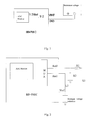
- FIG.1 shows an ADC calibration circuit diagram according to the prior art:
- BB+PMIC are baseband chip and power management chip; the baseband chip BB primarily runs software and is responsible for ADC acquisition; the power management chip PMIC primarily reduces battery voltage by one half and then inputs it to the ADC module.
- the reference voltage for ADC modules is 2.8 V or 2.6 V, while the highest battery voltage can reach 4.2 V, which exceeds the range of reference voltage for ADC modules. If the battery voltage is reduced by one half, the highest voltage input into the ADC module will be 2.1 V, which is lower than the reference voltage for ADC modules and falls into the range of reference voltage for ADC modules.
- an external reference voltage source is applied on the input pins VBAT and GND of a cell phone unit; the voltage amplitudes of the external reference voltage source are set at 3.4 V and 4.2 V, respectively, which are sampled by BB+PMIC, respectively, to obtain corresponding digital values. Based on these two digital values, the corresponding voltage - digital value straight line can be computed for the ADC module, with which a subsequently sampled digital value of certain point can be determined exclusively and accurately to the voltage value thereof.
- the object of the present invention is to provide a calibration device for ADC module in a mobile terminal, intending to perform ADC calibration without external reference voltage source so as to reduce calibration errors and improve calibration efficiency.
- An embodiment of the present invention is carried out in this way: a calibration device for ADC module in a mobile terminal, said ADC module being disposed inside a baseband chip,
- Another object of the embodiment of the present invention is to provide a mobile terminal, said terminal comprises a calibration device for ADC module and said ADC module is disposed inside a baseband chip,
- the embodiment of the present invention uses a bandgap voltage reference inside the mobile terminal platform to provide voltage to the ADC module, which, during the ADC module calibration, does not require an external reference voltage source to perform the ADC calibration, and therefore greatly reduces calibration errors and improves calibration efficiency.
- Fig.2 illustrates the structure of a calibration device for ADC module in a mobile terminal according to an embodiment of the present invention.
- Said ADC module is disposed inside a baseband chip BB or a power management chip PMIC, and said device further comprises a bandgap voltage reference inside the mobile terminal platform for generating a reference voltage Vref.
- Said device further comprises a circuit for connecting said bandgap voltage reference, said circuit being connected with said ADC module for providing the reference voltage generated by said bandgap voltage reference to said ADC module.
- Said circuit comprises a first circuit L1 and a second circuit L2, a multiplexer switch MUX is further disposed inside said baseband chip, said multiplexer switch MUX is connected with said ADC module, and said first circuit L1 and said second circuit L2 are connected with said multiplexer switch, respectively.
- a first input channel Ain0 and a second input channel Ain1 are further disposed inside said baseband chip, said first circuit L1 is connected with said multiplexer switch via said first input channel Ain0, and said second circuit L2 is connected with said multiplexer switch MUX via said second input channel Ain1.
- Said first circuit L1 and said second circuit L2 are further connected with said bandgap voltage reference, respectively.
- Vref is a reference voltage for the mobile terminal PMIC. Said voltage is generated by the bandgap voltage reference and is 1.2 V; the bandgap voltage reference inside the mobile terminal platform is very accurate and used as the reference power source for the entire power system of the mobile terminal.
- the embodiment of the present invention divides Vref into two paths, one of which directly enters the second input channel Ain1 of the ADC in the baseband chip and the other one generates a 0.6 V voltage input via division by the resistor R1 and the resistor R2 and then inputs into the first input channel Ain0.
- the resistor R1 and the resistor R2 are 100 K, respectively.
- MUX is a multiplexer switch. Since there is only one ADC module, it is necessary to use the multiplexer switch MUX to decide which analog input will be sampled.
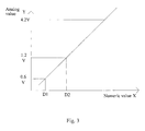
- Fig.2 illustrates the functional relationship between analog voltage and digital voltage during the ADC module calibration according to the embodiment of the present invention.
- the x axis is digital value obtained from ADC sampling, and the y axis corresponds to analog voltage value:
- the embodiment of the present invention further provides a mobile terminal and said terminal comprises the calibration device for ADC module disposed inside the mobile terminal according to the embodiment of the present invention, which will not be described herein because of the detailed description of said device above.
- the embodiment of the present invention uses a bandgap voltage reference inside the mobile terminal platform to provide voltage to the ADC module, which, during the ADC module calibration, does not require an external reference voltage source to perform the ADC calibration, and therefore greatly reduces calibration errors and improves calibration efficiency.
Landscapes
- Engineering & Computer Science (AREA)
- Theoretical Computer Science (AREA)
- Analogue/Digital Conversion (AREA)
- Control Of Electrical Variables (AREA)
Abstract
Description
- The present invention relates to the field of mobile terminal technology and specifically, to a calibration device for mobile terminal and ADC module thereof.
- Along with continuous development of mobile terminal technologies, users are imposing higher and higher requirements on mobile terminal functions.
- In current processes of R&D and production of cell phone products, all cell phones have errors in analog-to-digital converter (ADC) sampling due to discrete parameters of the selected electronic parts. As a result, ADC calibration needs to be performed on every cell phone unit in R&D or production.
- Please refer to
Fig.1 , which shows an ADC calibration circuit diagram according to the prior art: - BB+PMIC are baseband chip and power management chip; the baseband chip BB primarily runs software and is responsible for ADC acquisition; the power management chip PMIC primarily reduces battery voltage by one half and then inputs it to the ADC module. The reference voltage for ADC modules is 2.8 V or 2.6 V, while the highest battery voltage can reach 4.2 V, which exceeds the range of reference voltage for ADC modules. If the battery voltage is reduced by one half, the highest voltage input into the ADC module will be 2.1 V, which is lower than the reference voltage for ADC modules and falls into the range of reference voltage for ADC modules.
- In
Fig.1 , an external reference voltage source is applied on the input pins VBAT and GND of a cell phone unit; the voltage amplitudes of the external reference voltage source are set at 3.4 V and 4.2 V, respectively, which are sampled by BB+PMIC, respectively, to obtain corresponding digital values. Based on these two digital values, the corresponding voltage - digital value straight line can be computed for the ADC module, with which a subsequently sampled digital value of certain point can be determined exclusively and accurately to the voltage value thereof. - From the above process, it can be seen that said calibration process must be carried out with an external reference voltage source. Moreover, time is required for the operation of the external reference voltage source. Said time is a part of the production time of cell phones. The elimination of this time can increase the production rate of cell phones; at the same time, the presence of precision errors of an external reference voltage source can directly lead to errors in ADC module calibration and affect the accuracy to identify external analog signals by the software.
- How to provide a method of ADC calibration without external reference voltage source so as to reduce calibration errors and improve calibration efficiency is one of the research directions in the field of mobile terminal production technologies.
- The object of the present invention is to provide a calibration device for ADC module in a mobile terminal, intending to perform ADC calibration without external reference voltage source so as to reduce calibration errors and improve calibration efficiency.
- An embodiment of the present invention is carried out in this way: a calibration device for ADC module in a mobile terminal, said ADC module being disposed inside a baseband chip,
- Said device further comprises a bandgap voltage reference inside the mobile terminal platform for generating a reference voltage;
- Said device further comprises a circuit for connecting said bandgap voltage reference, said circuit being connected with said ADC module for providing the reference voltage generated by said bandgap voltage reference to said ADC module.
- Another object of the embodiment of the present invention is to provide a mobile terminal, said terminal comprises a calibration device for ADC module and said ADC module is disposed inside a baseband chip,
- Said device further comprises a bandgap voltage reference inside the mobile terminal platform for generating a reference voltage;
- Said device further comprises a circuit for connecting said bandgap voltage reference, said circuit being connected with said ADC module for providing the reference voltage generated by said bandgap voltage reference to said ADC module.
- The embodiment of the present invention uses a bandgap voltage reference inside the mobile terminal platform to provide voltage to the ADC module, which, during the ADC module calibration, does not require an external reference voltage source to perform the ADC calibration, and therefore greatly reduces calibration errors and improves calibration efficiency.
-
- Fig.1
- shows a calibration circuit diagram for ADC module in a mobile terminal according to the prior art;
- Fig.2
- illustrates the structure of a calibration device for ADC module in a mobile terminal according to an embodiment of the present invention;
- Fig.3
- illustrates the functional relationship between analog voltage and digital voltage during the ADC module calibration according to an embodiment of the present invention.
- To make the objects, technology and advantages of the present invention more clearly understood, the present invention is further described in detail below with reference to the accompanying drawings and an embodiment. It should be understood that the specific embodiment described herein is only intended to explain the present invention, not to limit the present invention.
-
Fig.2 illustrates the structure of a calibration device for ADC module in a mobile terminal according to an embodiment of the present invention. - Said ADC module is disposed inside a baseband chip BB or a power management chip PMIC, and said device further comprises a bandgap voltage reference inside the mobile terminal platform for generating a reference voltage Vref.
- Said device further comprises a circuit for connecting said bandgap voltage reference, said circuit being connected with said ADC module for providing the reference voltage generated by said bandgap voltage reference to said ADC module.
- Said circuit comprises a first circuit L1 and a second circuit L2, a multiplexer switch MUX is further disposed inside said baseband chip, said multiplexer switch MUX is connected with said ADC module, and said first circuit L1 and said second circuit L2 are connected with said multiplexer switch, respectively.
- A first input channel Ain0 and a second input channel Ain1 are further disposed inside said baseband chip, said first circuit L1 is connected with said multiplexer switch via said first input channel Ain0, and said second circuit L2 is connected with said multiplexer switch MUX via said second input channel Ain1.
- Said first circuit L1 and said second circuit L2 are further connected with said bandgap voltage reference, respectively.
- In
Fig.2 , Vref is a reference voltage for the mobile terminal PMIC. Said voltage is generated by the bandgap voltage reference and is 1.2 V; the bandgap voltage reference inside the mobile terminal platform is very accurate and used as the reference power source for the entire power system of the mobile terminal. - The embodiment of the present invention divides Vref into two paths, one of which directly enters the second input channel Ain1 of the ADC in the baseband chip and the other one generates a 0.6 V voltage input via division by the resistor R1 and the resistor R2 and then inputs into the first input channel Ain0. Wherein, the resistor R1 and the resistor R2 are 100 K, respectively.
- In
Fig.2 , MUX is a multiplexer switch. Since there is only one ADC module, it is necessary to use the multiplexer switch MUX to decide which analog input will be sampled. - It can be seen from
Fig.2 that by sampling the analog first input channel Ain0 and the second input channel Ain1, digital values corresponding to 1.2 V and 0.6 V can be obtained. Please refer toFig.3. Fig.3 illustrates the functional relationship between analog voltage and digital voltage during the ADC module calibration according to the embodiment of the present invention. The x axis is digital value obtained from ADC sampling, and the y axis corresponds to analog voltage value: - Assume that the digital value obtained from ADC sampling corresponding to 0.6 V is D1 and the digital value corresponding to 1.2 V is D2, then the straight line equation in
Fig.3 is:

- It can be seen from

- The embodiment of the present invention further provides a mobile terminal and said terminal comprises the calibration device for ADC module disposed inside the mobile terminal according to the embodiment of the present invention, which will not be described herein because of the detailed description of said device above.
- The embodiment of the present invention uses a bandgap voltage reference inside the mobile terminal platform to provide voltage to the ADC module, which, during the ADC module calibration, does not require an external reference voltage source to perform the ADC calibration, and therefore greatly reduces calibration errors and improves calibration efficiency.
- It should be understood that those skilled in the art may make improvements or modifications according to the above description, while all these improvements and modifications shall be encompassed by the claims of the present invention.
Claims (8)
- A calibration device for an ADC module in a mobile terminal, said ADC module being disposed inside a baseband chip, characterized in that,- Said device further comprises a bandgap voltage reference inside the mobile terminal platform for generating a reference voltage;- Said device further comprises a circuit for connecting said bandgap voltage reference, said circuit being connected with said ADC module for providing the reference voltage generated by said bandgap voltage reference to said ADC module.
- The calibration device for an ADC module in a mobile terminal as set forth in Claim 1, characterized in that,- Said circuit comprises a first circuit and a second circuit, a multiplexer switch is further disposed inside said baseband chip, said multiplexer switch is connected with said ADC module, and said first circuit and said second circuit are connected with said multiplexer switch, respectively.
- The calibration device for an ADC module in a mobile terminal as set forth in Claim 2, characterized in that,- A first input channel and a second input channel are further disposed inside said baseband chip, said first circuit is connected with said multiplexer switch via said first input channel, and said second circuit is connected with said multiplexer switch via said second input channel.
- The calibration device for an ADC module in a mobile terminal as set forth in Claim 2, characterized in that said first circuit and said second circuit are connected with said bandgap voltage reference, respectively.
- A mobile terminal, characterized in that said terminal comprises a calibration device for ADC module and said ADC module is disposed inside a baseband chip,- Said device further comprises a bandgap voltage reference inside the mobile terminal platform for generating a reference voltage;- Said device further comprises a circuit for connecting said bandgap voltage reference, said circuit being connected with said ADC module for providing the reference voltage generated by said bandgap voltage reference to said ADC module.
- The mobile terminal as set forth in Claim 5, characterized in that said circuit comprises a first circuit and a second circuit, a multiplexer switch is further disposed inside said baseband chip, said multiplexer switch is connected with said ADC module, and said first circuit and said second circuit are connected with said multiplexer switch, respectively.
- The mobile terminal as set forth in Claim 6, characterized in that a first input channel and a second input channel are further disposed inside said baseband chip, said first circuit is connected with said multiplexer switch via said first input channel, and said second circuit is connected with said multiplexer switch via said second input channel.
- The mobile terminal as set forth in Claim 6, characterized in that said first circuit and said second circuit are connected with said bandgap voltage reference, respectively.
Applications Claiming Priority (2)
| Application Number | Priority Date | Filing Date | Title |
|---|---|---|---|
| CN201010256175.0A CN101931409B (en) | 2010-08-17 | 2010-08-17 | Mobile terminal and calibrating device for analog-to-digital converter (ADC) module thereof |
| PCT/CN2011/074211 WO2012022175A1 (en) | 2010-08-17 | 2011-05-18 | Mobile terminal and calibration device for analog-to-digital conversion (adc) module thereof |
Publications (2)
| Publication Number | Publication Date |
|---|---|
| EP2607979A1 true EP2607979A1 (en) | 2013-06-26 |
| EP2607979A4 EP2607979A4 (en) | 2017-07-19 |
Family
ID=43370373
Family Applications (1)
| Application Number | Title | Priority Date | Filing Date |
|---|---|---|---|
| EP11817702.1A Ceased EP2607979A4 (en) | 2010-08-17 | 2011-05-18 | Mobile terminal and calibration device for analog-to-digital conversion (adc) module thereof |
Country Status (4)
| Country | Link |
|---|---|
| US (1) | US8547261B2 (en) |
| EP (1) | EP2607979A4 (en) |
| CN (1) | CN101931409B (en) |
| WO (1) | WO2012022175A1 (en) |
Families Citing this family (7)
| Publication number | Priority date | Publication date | Assignee | Title |
|---|---|---|---|---|
| CN101931409B (en) | 2010-08-17 | 2013-08-14 | 惠州Tcl移动通信有限公司 | Mobile terminal and calibrating device for analog-to-digital converter (ADC) module thereof |
| US8416105B2 (en) * | 2011-02-17 | 2013-04-09 | Taiwan Semiconductor Manufacturing Company, Ltd. | ADC calibration apparatus |
| DE102012222935B4 (en) * | 2011-12-16 | 2023-03-16 | Lear Corporation | Method and system for monitoring a converter voltage reference variation |
| CN104660258A (en) * | 2013-11-21 | 2015-05-27 | 上海航空电器有限公司 | Analog acquisition circuit with automatic calibration function and calibration method of analog acquisition circuit |
| US10156596B2 (en) * | 2015-12-10 | 2018-12-18 | Microchip Technology Incorporated | Voltage measurement circuit |
| CN109388171B (en) * | 2018-12-10 | 2024-02-09 | 上海艾为电子技术股份有限公司 | Band gap reference voltage source and electronic equipment |
| CN110531296B (en) * | 2019-08-09 | 2022-05-10 | 格威半导体(厦门)有限公司 | Gain calibration method of battery management system |
Family Cites Families (17)
| Publication number | Priority date | Publication date | Assignee | Title |
|---|---|---|---|---|
| US5440305A (en) * | 1992-08-31 | 1995-08-08 | Crystal Semiconductor Corporation | Method and apparatus for calibration of a monolithic voltage reference |
| US5822225A (en) * | 1994-09-21 | 1998-10-13 | Ericsson Raynet Corporation | Self-calibrating data processors and methods for calibrating same |
| TW294786B (en) * | 1995-09-11 | 1997-01-01 | Microchip Tech Inc | Digital trimming of on-chip analog components |
| US6462526B1 (en) * | 2001-08-01 | 2002-10-08 | Maxim Integrated Products, Inc. | Low noise bandgap voltage reference circuit |
| DE10392545B4 (en) * | 2002-05-08 | 2018-03-15 | Continental Teves Ag & Co. Ohg | Electronic circuitry for error-proof analog-to-digital conversion of signals |
| US7265529B2 (en) * | 2004-08-19 | 2007-09-04 | Micron Technologgy, Inc. | Zero power start-up circuit |
| US7558539B2 (en) * | 2005-09-30 | 2009-07-07 | Freescale Semiconductor, Inc. | Power control feedback loop for adjusting a magnitude of an output signal |
| TWI349489B (en) * | 2006-09-07 | 2011-09-21 | Realtek Semiconductor Corp | Image processing device and method |
| US7439608B2 (en) * | 2006-09-22 | 2008-10-21 | Intel Corporation | Symmetric bipolar junction transistor design for deep sub-micron fabrication processes |
| US7710303B2 (en) * | 2007-04-17 | 2010-05-04 | Microchip Technology Incorporated | Analog-to-digital converter offset and gain calibration using internal voltage references |
| CN101145780A (en) | 2007-06-01 | 2008-03-19 | 中兴通讯股份有限公司 | A method and device for testing the digital-to-analog conversion function of a digital-to-analog conversion chip |
| CN101686057B (en) * | 2008-09-28 | 2012-02-29 | 扬智科技股份有限公司 | Digital to Analog Converter |
| CN101393466B (en) * | 2008-10-30 | 2010-11-17 | 上海交通大学 | Fully integrated low-noise power system in RF receiver chip |
| US8248280B2 (en) * | 2009-09-29 | 2012-08-21 | Silicon Laboratories Inc. | Successive approximation register (SAR) analog-to-digital converter (ADC) having optimized filter |
| CN101764610A (en) | 2009-12-23 | 2010-06-30 | 中国航空工业集团公司第六三一研究所 | Hardware and software implementation method for improving digital-analog/analog-digital conversion accuracy |
| CN101931409B (en) | 2010-08-17 | 2013-08-14 | 惠州Tcl移动通信有限公司 | Mobile terminal and calibrating device for analog-to-digital converter (ADC) module thereof |
| CN201813361U (en) * | 2010-08-17 | 2011-04-27 | 惠州Tcl移动通信有限公司 | Analog-to-digital conversion (ADC) module calibrating device and mobile terminal |
-
2010
- 2010-08-17 CN CN201010256175.0A patent/CN101931409B/en active Active
-
2011
- 2011-05-18 EP EP11817702.1A patent/EP2607979A4/en not_active Ceased
- 2011-05-18 US US13/505,542 patent/US8547261B2/en active Active
- 2011-05-18 WO PCT/CN2011/074211 patent/WO2012022175A1/en not_active Ceased
Non-Patent Citations (1)
| Title |
|---|
| See references of WO2012022175A1 * |
Also Published As
| Publication number | Publication date |
|---|---|
| WO2012022175A1 (en) | 2012-02-23 |
| US8547261B2 (en) | 2013-10-01 |
| EP2607979A4 (en) | 2017-07-19 |
| US20120223848A1 (en) | 2012-09-06 |
| CN101931409A (en) | 2010-12-29 |
| CN101931409B (en) | 2013-08-14 |
Similar Documents
| Publication | Publication Date | Title |
|---|---|---|
| US8547261B2 (en) | Calibration device for mobile terminal and ADC module thereof | |
| EP4246803A1 (en) | On-chip rc oscillator, chip, and communication terminal | |
| CN102353836B (en) | Method for dynamically adjusting current channel gain of wide-range electric energy meter | |
| US9337858B2 (en) | Data processing system | |
| CN103091552B (en) | Pre-calibrated electric energy metering circuit and calibration steps | |
| CN102207535B (en) | Circuit structure and method for automatically testing analog baseband chip comprising analog-digital converter (ADC) and digital-analog converter (DAC) | |
| US10168719B2 (en) | Digital low dropout regulator and control method thereof | |
| CN106888020A (en) | DAC switchs the digital measurement of mismatch error | |
| US11579106B2 (en) | High accuracy impedance measurement | |
| CN107656572B (en) | Multi-path adjustable voltage source realized by digital-to-analog converter and control method thereof | |
| CN101668057A (en) | Terminal and system with function of multimeter | |
| US20160182076A1 (en) | Background Calibration for Digital-to-Analog Converters | |
| CN201813361U (en) | Analog-to-digital conversion (ADC) module calibrating device and mobile terminal | |
| US12524029B2 (en) | Digital-analog integrated voltage transformer calibration system | |
| CN117590730A (en) | An ultra-high-precision second pulse and 10MHZ signal measurement circuit and method | |
| CN112147532B (en) | A passive electronic load circuit | |
| CN104135275A (en) | A signal isolator and a method for debugging the signal isolator | |
| US12456987B2 (en) | Analog-to-digital conversion circuit, integrated chip, display device, and analog-to-digital conversion method | |
| CN2601395Y (en) | Digitized weighting module | |
| JP2011040985A (en) | A-d converter | |
| CN114257244A (en) | ADC chip testing circuit, method, testing equipment and storage medium | |
| CN118523755B (en) | Pulse output method, device, source meter and storage medium | |
| EP4657099A1 (en) | Detection circuit and method for detecting internal resistance of battery unit | |
| CN118523621B (en) | Four-quadrant power supply adjustment circuit, method, device, source meter and storage medium | |
| RU2389072C1 (en) | Analog multiplier of two signals |
Legal Events
| Date | Code | Title | Description |
|---|---|---|---|
| PUAI | Public reference made under article 153(3) epc to a published international application that has entered the european phase |
Free format text: ORIGINAL CODE: 0009012 |
|
| 17P | Request for examination filed |
Effective date: 20130308 |
|
| AK | Designated contracting states |
Kind code of ref document: A1 Designated state(s): AL AT BE BG CH CY CZ DE DK EE ES FI FR GB GR HR HU IE IS IT LI LT LU LV MC MK MT NL NO PL PT RO RS SE SI SK SM TR |
|
| DAX | Request for extension of the european patent (deleted) | ||
| RA4 | Supplementary search report drawn up and despatched (corrected) |
Effective date: 20170619 |
|
| RIC1 | Information provided on ipc code assigned before grant |
Ipc: H03M 1/12 20060101ALN20170612BHEP Ipc: H03M 1/10 20060101AFI20170612BHEP |
|
| STAA | Information on the status of an ep patent application or granted ep patent |
Free format text: STATUS: EXAMINATION IS IN PROGRESS |
|
| 17Q | First examination report despatched |
Effective date: 20200810 |
|
| REG | Reference to a national code |
Ref country code: DE Ref legal event code: R003 |
|
| STAA | Information on the status of an ep patent application or granted ep patent |
Free format text: STATUS: THE APPLICATION HAS BEEN REFUSED |
|
| 18R | Application refused |
Effective date: 20211014 |