EP2605624A1 - Flexible flat cable - Google Patents
Flexible flat cable Download PDFInfo
- Publication number
- EP2605624A1 EP2605624A1 EP12184784.2A EP12184784A EP2605624A1 EP 2605624 A1 EP2605624 A1 EP 2605624A1 EP 12184784 A EP12184784 A EP 12184784A EP 2605624 A1 EP2605624 A1 EP 2605624A1
- Authority
- EP
- European Patent Office
- Prior art keywords
- flat cable
- insulator layer
- layer
- flexible flat
- shield member
- Prior art date
- Legal status (The legal status is an assumption and is not a legal conclusion. Google has not performed a legal analysis and makes no representation as to the accuracy of the status listed.)
- Withdrawn
Links
- 239000012212 insulator Substances 0.000 claims abstract description 61
- 239000004020 conductor Substances 0.000 claims abstract description 52
- 239000000463 material Substances 0.000 claims abstract description 45
- 230000002787 reinforcement Effects 0.000 claims abstract description 30
- 230000015572 biosynthetic process Effects 0.000 claims description 2
- 239000012774 insulation material Substances 0.000 description 4
- 238000009413 insulation Methods 0.000 description 3
- 230000005540 biological transmission Effects 0.000 description 2
- 238000006073 displacement reaction Methods 0.000 description 2
- 238000004519 manufacturing process Methods 0.000 description 2
- 238000012986 modification Methods 0.000 description 2
- 230000004048 modification Effects 0.000 description 2
- RYGMFSIKBFXOCR-UHFFFAOYSA-N Copper Chemical compound [Cu] RYGMFSIKBFXOCR-UHFFFAOYSA-N 0.000 description 1
- 238000013459 approach Methods 0.000 description 1
- 229910052802 copper Inorganic materials 0.000 description 1
- 239000010949 copper Substances 0.000 description 1
- 230000003247 decreasing effect Effects 0.000 description 1
- 238000005530 etching Methods 0.000 description 1
- 239000011888 foil Substances 0.000 description 1
- 239000011159 matrix material Substances 0.000 description 1
- 229920001225 polyester resin Polymers 0.000 description 1
- 239000004645 polyester resin Substances 0.000 description 1
- 230000008054 signal transmission Effects 0.000 description 1
- 239000000758 substrate Substances 0.000 description 1
- 230000000007 visual effect Effects 0.000 description 1
Images


Classifications
-
- H—ELECTRICITY
- H01—ELECTRIC ELEMENTS
- H01B—CABLES; CONDUCTORS; INSULATORS; SELECTION OF MATERIALS FOR THEIR CONDUCTIVE, INSULATING OR DIELECTRIC PROPERTIES
- H01B7/00—Insulated conductors or cables characterised by their form
- H01B7/08—Flat or ribbon cables
-
- H—ELECTRICITY
- H05—ELECTRIC TECHNIQUES NOT OTHERWISE PROVIDED FOR
- H05K—PRINTED CIRCUITS; CASINGS OR CONSTRUCTIONAL DETAILS OF ELECTRIC APPARATUS; MANUFACTURE OF ASSEMBLAGES OF ELECTRICAL COMPONENTS
- H05K1/00—Printed circuits
- H05K1/02—Details
- H05K1/0213—Electrical arrangements not otherwise provided for
- H05K1/0237—High frequency adaptations
- H05K1/025—Impedance arrangements, e.g. impedance matching, reduction of parasitic impedance
- H05K1/0253—Impedance adaptations of transmission lines by special lay-out of power planes, e.g. providing openings
-
- H—ELECTRICITY
- H01—ELECTRIC ELEMENTS
- H01B—CABLES; CONDUCTORS; INSULATORS; SELECTION OF MATERIALS FOR THEIR CONDUCTIVE, INSULATING OR DIELECTRIC PROPERTIES
- H01B7/00—Insulated conductors or cables characterised by their form
- H01B7/04—Flexible cables, conductors, or cords, e.g. trailing cables
-
- H—ELECTRICITY
- H05—ELECTRIC TECHNIQUES NOT OTHERWISE PROVIDED FOR
- H05K—PRINTED CIRCUITS; CASINGS OR CONSTRUCTIONAL DETAILS OF ELECTRIC APPARATUS; MANUFACTURE OF ASSEMBLAGES OF ELECTRICAL COMPONENTS
- H05K1/00—Printed circuits
- H05K1/02—Details
- H05K1/0213—Electrical arrangements not otherwise provided for
- H05K1/0216—Reduction of cross-talk, noise or electromagnetic interference
- H05K1/0218—Reduction of cross-talk, noise or electromagnetic interference by printed shielding conductors, ground planes or power plane
- H05K1/0224—Patterned shielding planes, ground planes or power planes
- H05K1/0225—Single or multiple openings in a shielding, ground or power plane
-
- H—ELECTRICITY
- H05—ELECTRIC TECHNIQUES NOT OTHERWISE PROVIDED FOR
- H05K—PRINTED CIRCUITS; CASINGS OR CONSTRUCTIONAL DETAILS OF ELECTRIC APPARATUS; MANUFACTURE OF ASSEMBLAGES OF ELECTRICAL COMPONENTS
- H05K1/00—Printed circuits
- H05K1/02—Details
- H05K1/11—Printed elements for providing electric connections to or between printed circuits
- H05K1/118—Printed elements for providing electric connections to or between printed circuits specially for flexible printed circuits, e.g. using folded portions
-
- H—ELECTRICITY
- H05—ELECTRIC TECHNIQUES NOT OTHERWISE PROVIDED FOR
- H05K—PRINTED CIRCUITS; CASINGS OR CONSTRUCTIONAL DETAILS OF ELECTRIC APPARATUS; MANUFACTURE OF ASSEMBLAGES OF ELECTRICAL COMPONENTS
- H05K2201/00—Indexing scheme relating to printed circuits covered by H05K1/00
- H05K2201/07—Electric details
- H05K2201/0707—Shielding
- H05K2201/0715—Shielding provided by an outer layer of PCB
-
- H—ELECTRICITY
- H05—ELECTRIC TECHNIQUES NOT OTHERWISE PROVIDED FOR
- H05K—PRINTED CIRCUITS; CASINGS OR CONSTRUCTIONAL DETAILS OF ELECTRIC APPARATUS; MANUFACTURE OF ASSEMBLAGES OF ELECTRICAL COMPONENTS
- H05K2201/00—Indexing scheme relating to printed circuits covered by H05K1/00
- H05K2201/09—Shape and layout
- H05K2201/09209—Shape and layout details of conductors
- H05K2201/09654—Shape and layout details of conductors covering at least two types of conductors provided for in H05K2201/09218 - H05K2201/095
- H05K2201/09681—Mesh conductors, e.g. as a ground plane
-
- H—ELECTRICITY
- H05—ELECTRIC TECHNIQUES NOT OTHERWISE PROVIDED FOR
- H05K—PRINTED CIRCUITS; CASINGS OR CONSTRUCTIONAL DETAILS OF ELECTRIC APPARATUS; MANUFACTURE OF ASSEMBLAGES OF ELECTRICAL COMPONENTS
- H05K2201/00—Indexing scheme relating to printed circuits covered by H05K1/00
- H05K2201/09—Shape and layout
- H05K2201/09209—Shape and layout details of conductors
- H05K2201/09654—Shape and layout details of conductors covering at least two types of conductors provided for in H05K2201/09218 - H05K2201/095
- H05K2201/0969—Apertured conductors
-
- H—ELECTRICITY
- H05—ELECTRIC TECHNIQUES NOT OTHERWISE PROVIDED FOR
- H05K—PRINTED CIRCUITS; CASINGS OR CONSTRUCTIONAL DETAILS OF ELECTRIC APPARATUS; MANUFACTURE OF ASSEMBLAGES OF ELECTRICAL COMPONENTS
- H05K2201/00—Indexing scheme relating to printed circuits covered by H05K1/00
- H05K2201/20—Details of printed circuits not provided for in H05K2201/01 - H05K2201/10
- H05K2201/2009—Reinforced areas, e.g. for a specific part of a flexible printed circuit
Definitions
- the present invention relates to a flexible flat cable.
- a flexible flat cable (to be referred to as "a flat cable” hereinafter) is used in internal wiring of various electric devices and electronic instruments such as a computer.
- the flat cable as being formed in a band-like shape, has good flexibility and provides easy handling of wiring thereof within the instrument. Further, as the flat cable has only a small cross sectional area, it is suitable for use in a small instrument also.
- a flat cable comprising: a plurality of flat-plate like conductors spaced part from each other with a predetermined gap therebetween and arranged in parallel with each other; first and second insulator layers sandwiching and covering the plurality of conductors therebetween, with exposing portions of the opposed ends of the conductors for allowing contact thereof with predetermined signal terminals; a first adjustment material layer provided on the side of the first insulator layer opposite the plurality of conductors and having insulation property; a ground layer provided only at the end of the side of the first adjustment material layer opposite the first insulator layer and coming into contact with a ground terminal having the ground potential; and a first shield layer provided on the side of the first adjustment material layer opposite the first insulator layer and electrically conductive to the ground layer; wherein the first adjustment material layer adjusts such that at the end, the distance between the conductors and the first shield layer is equal to the distance between the conductors and the ground layer (see Japanese Patent No. 4363664
- the ground layer is provided from the end of the flat cable, that is, from the position overlapped with the reinforcement plate, it becomes possible to place the conductor-side contact of the connector in agreement/alignment with the ground-side contact of the connector. In this case, however, there occurs impedance reduction at the position of the reinforcement plate.
- the present invention has been made in view of the above-described state of the art.
- the object of the invention is to provide a flexible flat cable that allows easy adjustment of impedance at the end.
- a flexible flat cable comprising:
- the plurality of linear conductors arranged in parallel with each other are covered as being sandwiched between the first insulator layer and the second insulator layer.
- the second insulator layer does not cover the conductors along the entire lengths thereof, but leaves the conductors being exposed at the end of the flexible flat cable.
- the shield member too is exposed at the end of the flexible flat cable. Therefore, the signal terminals and the ground terminal of the connector can be arranged in opposition to each other. This prevents occurrence of easy inadvertent detachment of the connector.
- the shield member includes an impedance adjusting means, it is possible to adjust the impedance at the end of the flexible flat cable to a desired value.
- the impedance adjusting means can be realized by e.g. decreasing the surface area of the side of the shield member opposite the reinforcement member. As the impedance depends on the surface area of the shield member, a desired impedance can be obtained by varying the area.
- a gap is formed between the reinforcement plate and the first adjustment material layer; the shield member comes into contact with the first insulator layer at the gap; and the rate of decrease in the area at the gap is set greater than the rate of decrease in the area at the portion of the shield member covering the reinforcement member.
- the decrease of the area of the shield member can be realized by e.g. forming a through hole extending through the shield member. As such through hole can be easily formed, a desired impedance can be obtained without inviting manufacture cost increase.
- the through hole can be provided at various positions. Preferably, however, the through hole can be formed e.g. at the position overlapped with the conductor as seen in the plane view. With formation of the through hole in this manner, impedance adjustment can be further facilitated.
- the flexible flat cable further comprises:
- Fig. 1 is a plane view of the flat cable 1 as seen from the side of a second insulator layer 13 to be described later
- Fig. 2 is a section view showing the vicinity of an end of the flat cable 1.
- the flat cable 1 includes a plurality of linear or line-like conductors 11 arranged in parallel with each other. These conductors 11 each forms a signal line for transmitting signals. The number of conductors 11 will be determined in accordance with the specification of signals to be transmitted. As the material forming the conductors 11, a material having high conductivity and flexibility such as copper is preferred. Further, as these conductors 11, a plurality of linear conductors may be employed or the conductors may be formed as a plurality of linear portions formed by e.g. etching a conductive foil formed on a highly flexible substrate.
- the conductors 11 are sandwiched between a first insulator layer 12 and the second insulator layer 13 and covered/shielded thereby.
- a polyester resin can be used as material forming the first insulator layer 12 and the second insulator layer 13.
- the side of the conductor 11 on the side of the first insulator layer 12 will be referred to as the upper side and the side thereof on the side of the second insulator layer 13 will be referred to as the lower side, respectively.
- the length of the first insulator layer 12 is same as the length of the conductors 11, whereas the length of the second insulator layer 13 is shorter than the length of the conductors 11.
- the conductors 11 are covered by the first insulator layer 12, but not covered by the second insulator layer 13. That is, the conductors 11 remain exposed at the end of the flat cable 1 to the lower side (to the side of the second insulator layer 13).
- first adjustment material layer 14 Upwardly of the first insulator layer 12, there is provided a first adjustment material layer 14 having insulating property. This first adjustment material layer 14 is spaced from the end of the flat cable 1 with a predetermined distance. More particularly, between the first adjustment material layer 14 and the end of the flat cable 1, a gap is formed. Incidentally, in the following discussion, the portion where the first adjustment material layer 14 is provided will be referred to as the "region (c)".
- a reinforcement plate 18 for increasing the strength of the end of the flat cable 1.
- This reinforcement plate 18 is provided at the gap between the first adjustment material layer 14 and the end of the flat cable 1.
- the reinforcement plate 18 and the first adjustment material layer 14 are not in contact with each other, but a gap 1a is formed between the reinforcement plate 18 and the first adjustment material layer 14.
- the portion where the reinforcement plate 18 is provided will be referred to as the "region (a)” and the portion where the gap 1a is formed will be referred to as the "region (b)", respectively.
- this gap 1a between the reinforcement plate 18 and the first adjustment material layer 14 is not an essential requirement. This may be omitted if the flat cable 1 can be manufactured so as not to form such gap 1a.
- a conductive shield member 19 is provided at a position slightly retracted from the end so as no to protrude beyond the end of the flat cable 1.
- the gap 1a is present between the reinforcement plate 18 and the first adjustment material layer 14 and this gap 1a together with the first insulator layer 12 form a recess. Therefore, in the region (b), the shield member 19 is bent downwards so as to follow the contour of the recess and contacts the first insulator layer 12 which forms the bottom of this recess.
- first shield layer 16 having conductivity.
- This first shield layer 16 is provided at a position spaced from the end of the flat cable 1 by a predetermined distance. Therefore, the first adjustment material layer 14 as a whole is covered by the first shield layer 16, but the upper side of the shield member 19 on the side of the end of the flat cable 1 remains exposed.
- a connector 2 To the end of the flat cable 1 configured as described above, a connector 2 is connected.
- This connector 2 includes signal terminals 21 to be connected to the conductors 11 and a ground terminal 22 for transmitting a ground potential.
- each conductor 11 is exposed on the lower side thereof, whereas the shield member 19 is exposed on the upper side thereof. From the upper side, the ground terminal 22 comes into contact with the shield member 19 and from the lower side, the signal terminals 21 come into contact with the conductors 11. Therefore, as shown, the signal terminals 21 and the ground terminal 22 can be disposed at positions in opposition to each other. With this, the clamping force applied from the signal terminal 21 to the flat cable 1 and the clamping force applied from the ground terminal 22 to the flat cable 21 act in opposition to each other. Therefore, easy inadvertent detachment of the connector 2 can be effectively prevented.
- the impedance in the region (a), i.e. the vicinity of the end of the flat cable 1 is lower than the impedance in the region (c), i.e. the vicinity of the center portion of the flat cable 1.
- Such reduction in the impedance in the vicinity of the end of the flat cable 1 is not desirable, in particular in the case of high speed transmission such as described above.
- Fig. 3 is a plane view showing the vicinity of the end of the flat case 1 as seen from the upper side, that is, from the first insulator layer 12 side.
- slits 30a an example of "a through hole” in the present invention
- Fig. 4 is a section view of the flat cable 1 in section along the sectional line extending through the slit 30a. This view shows the condition of the slit 30a.
- the shield member 19 contacts the first insulator layer 12. Accordingly, as shown in Fig. 5 , the impedance reduction in the region (b) is greater than the impedance reduction in the area (a). Therefore, in the instant embodiment, as shown in Fig. 3 , the decrease rate of the surface area of the shield member 19 in the region (a) is set greater than the decrease rate of the surface area of the shield member 19 in the region (b). Specifically, the width of the slit 30a in the region (a) is set greater than the width of the slit 30a in the region (b).
- the impedances in the respective regions become as illustrated in Fig. 6 .
- the change in the impedances approaches flat.
- the positions where the slits 30a are formed can vary as desired. It is preferred, however, that the slits 30a be formed so as to be overlapped with the conductors 11 as seen in the plane view. Incidentally, in Fig. 3 , for the sake of ease of visual understanding, illustration of the conductors 11 is omitted. However, the slits 30a are formed so as to be overlapped with the conductors 11 as seen in the plane view. Also, in practice, as shown in Fig. 4 , the conductors 11 extend from one end of the flat cable 1 to the other end thereof. Also, the size of the slit 30a can be variably set in accordance with the magnitude of the impedance to be adjusted thereby.
- the shape of the through hole as the impedance adjusting means 30 is not limited to the slit, but can vary in many ways.
- rectangular holes 30b another example of the "through hole" in the present invention
- the impedance adjusting means 30 can be provided in a matrix pattern.
- rhombus-shaped holes 30c (another example of the "through hole" in the present invention) as the impedance adjusting means 30 can be provided in a checkerboard pattern.
- the shape and layout of the through holes as the impedance adjusting means 30 are not limited to the above, but various modifications thereof are possible as long as such modifications too achieve the intended object of the invention.
- the through holes be overlapped with the conductors 11 as seen in the plane view.
- the aperture area of the through hole(s) in the region (b) be greater than the aperture area of the through hole(s) in the region (a).
- the impedance adjusting means 30 is not limited to the through holes.
- an insulation layer may be formed in the shield member 19. I this case, the insulation layer can have a similar shape to the above-described through hole.
- the adjustment material layer (the first adjustment material layer 14) and the shield layer (the first shield layer 16) are provided only on the side of the first insulation material layer 12.
- a second adjustment material layer 15 may be provided under the insulation material layer 13 and a second shield layer 17 may be provided under the second adjustment material layer 15.
- the second shield layer 17 is arranged so as to cover the end of the second adjustment material layer 15. Further, the second shield layer 17 is formed shorter than the second insulation material layer 13, so that the end of the second insulation material layer 13 is exposed.
- the junction portion between the region (b) and the region (c) seems to be of a different layer thickness from the flat portions.
- the thickness is constant throughout all the regions or portions.
- the present invention is applicable to a flexible flat cable.
Landscapes
- Engineering & Computer Science (AREA)
- Microelectronics & Electronic Packaging (AREA)
- Insulated Conductors (AREA)
Abstract
Description
- The present invention relates to a flexible flat cable.
- In recent years, a flexible flat cable (to be referred to as "a flat cable" hereinafter) is used in internal wiring of various electric devices and electronic instruments such as a computer. The flat cable, as being formed in a band-like shape, has good flexibility and provides easy handling of wiring thereof within the instrument. Further, as the flat cable has only a small cross sectional area, it is suitable for use in a small instrument also.
- When such flat cable is to be used for high speed transmission, matching is needed between the impedance of the circuit and the impedance of the flat cable in order to avoid reduction in the signal transmission rate due to mismatch between the impedances. In particular, impedance change tends to occur due to the arrangement provided at the end of the flat cable for connection with a connector.
- For overcoming the above problem, for instance, there has been proposed a flat cable comprising: a plurality of flat-plate like conductors spaced part from each other with a predetermined gap therebetween and arranged in parallel with each other; first and second insulator layers sandwiching and covering the plurality of conductors therebetween, with exposing portions of the opposed ends of the conductors for allowing contact thereof with predetermined signal terminals; a first adjustment material layer provided on the side of the first insulator layer opposite the plurality of conductors and having insulation property; a ground layer provided only at the end of the side of the first adjustment material layer opposite the first insulator layer and coming into contact with a ground terminal having the ground potential; and a first shield layer provided on the side of the first adjustment material layer opposite the first insulator layer and electrically conductive to the ground layer; wherein the first adjustment material layer adjusts such that at the end, the distance between the conductors and the first shield layer is equal to the distance between the conductors and the ground layer (see Japanese Patent No.
4363664 - In the flat cable disclosed in this Japanese Patent No.
4363664 - As described above, with the flat cable disclosed in this Japanese Patent No.
4363664 4363664 Fig. 3 of Japanese Patent No.4363664 - On the other hand, if the ground layer is provided from the end of the flat cable, that is, from the position overlapped with the reinforcement plate, it becomes possible to place the conductor-side contact of the connector in agreement/alignment with the ground-side contact of the connector. In this case, however, there occurs impedance reduction at the position of the reinforcement plate.
- The present invention has been made in view of the above-described state of the art. The object of the invention is to provide a flexible flat cable that allows easy adjustment of impedance at the end.
- For accomplishing the above-noted object, according to the present invention, there is proposed a flexible flat cable comprising:
- a first sheet-like insulator layer;
- a second sheet-like insulator layer disposed in opposition to the first insulator layer;
- a plurality of linear conductors disposed in parallel with each other between the first insulator layer and the second insulator layer;
- a first adjustment material layer disposed on the side of the first insulator layer opposite the conductors and spaced from an end of the flexible flat cable with a predetermined distance;
- a reinforcement plate provided on the side of the first insulator layer opposite the conductors and between the end of the flexible flat cable and the first adjustment material layer;
- a shield member disposed so as to cover the side of the reinforcement plate opposite the first insulator layer and the side of the first adjustment material layer opposite the first insulator layer;
- a first shield layer disposed from the side of the shield member opposite the reinforcement plate to the side of the first adjustment material layer opposite the first insulator layer, with exposing a portion of the side of the shield member opposite the reinforcement plate;
- wherein the second insulator layer is arranged to expose the conductors at the end of the flexible flat cable;
- the exposed conductors and the exposed shield member come into contact with signal terminals and a ground terminal of a connector; and
- the shield member includes an impedance adjusting means.
- With the above-described arrangement, the plurality of linear conductors arranged in parallel with each other are covered as being sandwiched between the first insulator layer and the second insulator layer. But, the second insulator layer does not cover the conductors along the entire lengths thereof, but leaves the conductors being exposed at the end of the flexible flat cable. And, the shield member too is exposed at the end of the flexible flat cable. Therefore, the signal terminals and the ground terminal of the connector can be arranged in opposition to each other. This prevents occurrence of easy inadvertent detachment of the connector. Further, as the shield member includes an impedance adjusting means, it is possible to adjust the impedance at the end of the flexible flat cable to a desired value.
- The impedance adjusting means can be realized by e.g. decreasing the surface area of the side of the shield member opposite the reinforcement member. As the impedance depends on the surface area of the shield member, a desired impedance can be obtained by varying the area.
- Depending on the method of manufacturing the flexible flat cable, there may be formed a gap between the shield member and the first adjustment material layer. In such case, when the shield member comes into contact with the first insulator layer at the portion of such gap, impedance reduction occurs at this gap portion. Therefore, according to one preferred embodiment of the present invention, a gap is formed between the reinforcement plate and the first adjustment material layer; the shield member comes into contact with the first insulator layer at the gap; and the rate of decrease in the area at the gap is set greater than the rate of decrease in the area at the portion of the shield member covering the reinforcement member.
- With the above-described arrangement, with setting the area decrease rate of the shield member greater at the gap, impedance reduction at the gap portion can be restricted.
- The decrease of the area of the shield member can be realized by e.g. forming a through hole extending through the shield member. As such through hole can be easily formed, a desired impedance can be obtained without inviting manufacture cost increase.
- The through hole can be provided at various positions. Preferably, however, the through hole can be formed e.g. at the position overlapped with the conductor as seen in the plane view. With formation of the through hole in this manner, impedance adjustment can be further facilitated.
- According to another preferred embodiment of the flexible flat cable of the present invention, the flexible flat cable further comprises:
- a second adjustment material layer provided on the side of the second insulator layer opposite the conductors and spaced from the end of the flexible flat cable with a predetermined distance; and
- a second shield layer provided on the side of the second adjustment material layer opposite the second insulator layer and spaced from the end of the flexible flat cable with a predetermined distance.
- With the above-described arrangement, since the adjustment material layers and the shield layers are provided on the both sides of the conductors, impedance adjustment can be further facilitated.
-
- [
Fig. 1 ] is a plane view showing a flexible flat cable according to an embodiment of the present invention as seen from the side of a second insulator layer, - [
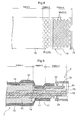
Fig. 2 ] is a section view showing the flexible flat cable according to the embodiment of the present invention, - [
Fig. 3 ] is a plane view showing the flexible flat cable according to the embodiment of the present invention as seen from the side of a first insulator layer, - [
Fig. 4 ] is a section view showing a flexible flat cable according to an embodiment of the present invention, - [
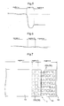
Fig. 5 ] is a view showing impedances at different positions of the flexible flat cable, - [
Fig. 6 ] is a view showing impedances at different positions of the flexible flat cable, - [
Fig. 7 ] is a plane view showing a flexible flat cable according to an embodiment of the present invention as seen from the side of a first insulator layer, - [
Fig. 8 ] is a plane view showing a flexible flat cable according to an embodiment of the present invention as seen from the side of a first insulator layer, - [
Fig. 9 ] is a section view of a flexible flat cable according to a further embodiment of the present invention. - Next, embodiments of a flexible flat cable (to be referred to as the "
flat cable 1" hereinafter) according to the present invention will be described with reference to the accompanying drawings.Fig. 1 is a plane view of theflat cable 1 as seen from the side of asecond insulator layer 13 to be described later, andFig. 2 is a section view showing the vicinity of an end of theflat cable 1. - As shown in
Fig. 1 , theflat cable 1 includes a plurality of linear or line-like conductors 11 arranged in parallel with each other. Theseconductors 11 each forms a signal line for transmitting signals. The number ofconductors 11 will be determined in accordance with the specification of signals to be transmitted. As the material forming theconductors 11, a material having high conductivity and flexibility such as copper is preferred. Further, as theseconductors 11, a plurality of linear conductors may be employed or the conductors may be formed as a plurality of linear portions formed by e.g. etching a conductive foil formed on a highly flexible substrate. - Further, as shown in
Fig. 2 , theconductors 11 are sandwiched between afirst insulator layer 12 and thesecond insulator layer 13 and covered/shielded thereby. As material forming thefirst insulator layer 12 and thesecond insulator layer 13, a polyester resin can be used. Incidentally, in the following discussion, with using the illustration inFig. 2 as a reference, the side of theconductor 11 on the side of thefirst insulator layer 12 will be referred to as the upper side and the side thereof on the side of thesecond insulator layer 13 will be referred to as the lower side, respectively. - As shown, the length of the
first insulator layer 12 is same as the length of theconductors 11, whereas the length of thesecond insulator layer 13 is shorter than the length of theconductors 11. Thus, at the end of theflat cable 1, theconductors 11 are covered by thefirst insulator layer 12, but not covered by thesecond insulator layer 13. That is, theconductors 11 remain exposed at the end of theflat cable 1 to the lower side (to the side of the second insulator layer 13). - Upwardly of the
first insulator layer 12, there is provided a firstadjustment material layer 14 having insulating property. This firstadjustment material layer 14 is spaced from the end of theflat cable 1 with a predetermined distance. More particularly, between the firstadjustment material layer 14 and the end of theflat cable 1, a gap is formed. Incidentally, in the following discussion, the portion where the firstadjustment material layer 14 is provided will be referred to as the "region (c)". - Further, upwardly of the
first insulator layer 12 ,there is provided areinforcement plate 18 for increasing the strength of the end of theflat cable 1. Thisreinforcement plate 18 is provided at the gap between the firstadjustment material layer 14 and the end of theflat cable 1. In the case of theflat cable 1 according to the present embodiment, thereinforcement plate 18 and the firstadjustment material layer 14 are not in contact with each other, but agap 1a is formed between thereinforcement plate 18 and the firstadjustment material layer 14. Incidentally, in the following discussion, the portion where thereinforcement plate 18 is provided will be referred to as the "region (a)" and the portion where thegap 1a is formed will be referred to as the "region (b)", respectively. - It is understood, however, that this
gap 1a between thereinforcement plate 18 and the firstadjustment material layer 14 is not an essential requirement. This may be omitted if theflat cable 1 can be manufactured so as not to formsuch gap 1a. - From the upper side of the
reinforcement plate 18 to the upper side of the end of the firstadjustment material layer 14, there is provided aconductive shield member 19. Thisshield member 19 is provided at a position slightly retracted from the end so as no to protrude beyond the end of theflat cable 1. As described above, thegap 1a is present between thereinforcement plate 18 and the firstadjustment material layer 14 and thisgap 1a together with thefirst insulator layer 12 form a recess. Therefore, in the region (b), theshield member 19 is bent downwards so as to follow the contour of the recess and contacts thefirst insulator layer 12 which forms the bottom of this recess. - Further, from the upper side of the
shield member 19 to the upper side of the firstadjustment material layer 14, there is provided afirst shield layer 16 having conductivity. Thisfirst shield layer 16 is provided at a position spaced from the end of theflat cable 1 by a predetermined distance. Therefore, the firstadjustment material layer 14 as a whole is covered by thefirst shield layer 16, but the upper side of theshield member 19 on the side of the end of theflat cable 1 remains exposed. - To the end of the
flat cable 1 configured as described above, aconnector 2 is connected. Thisconnector 2 includessignal terminals 21 to be connected to theconductors 11 and aground terminal 22 for transmitting a ground potential. As described above, eachconductor 11 is exposed on the lower side thereof, whereas theshield member 19 is exposed on the upper side thereof. From the upper side, theground terminal 22 comes into contact with theshield member 19 and from the lower side, thesignal terminals 21 come into contact with theconductors 11. Therefore, as shown, thesignal terminals 21 and theground terminal 22 can be disposed at positions in opposition to each other. With this, the clamping force applied from thesignal terminal 21 to theflat cable 1 and the clamping force applied from theground terminal 22 to theflat cable 21 act in opposition to each other. Therefore, easy inadvertent detachment of theconnector 2 can be effectively prevented. - With the
flat cable 1 configured as described above, as shown inFig. 5 , there occurs impedance change or variation in the regions (a), (c). Specifically, the impedance in the region (a), i.e. the vicinity of the end of theflat cable 1 is lower than the impedance in the region (c), i.e. the vicinity of the center portion of theflat cable 1. Such reduction in the impedance in the vicinity of the end of theflat cable 1 is not desirable, in particular in the case of high speed transmission such as described above. - To cope with the above, the
shield member 19 of the inventiveflat cable 1 is provided with an impedance adjusting means 30.Fig. 3 is a plane view showing the vicinity of the end of theflat case 1 as seen from the upper side, that is, from thefirst insulator layer 12 side. In this illustration, as the impedance adjusting means, slits 30a (an example of "a through hole" in the present invention) are provided. Eachslit 30a is arranged so as to extend through theshield member 19 in the regions (a), (b) from thefirst shield layer 16 side to thereinforcement plate 18 side.Fig. 4 is a section view of theflat cable 1 in section along the sectional line extending through theslit 30a. This view shows the condition of theslit 30a. - With provision of a through hole like the
slits 30a in theshield member 19 as described above, this effectively reduces the surface area of the upper side of theshield member 19, that is, the surface area of the side to which theground terminal 22 comes into contact. Therefore, in the vicinity of the region of the reduced surface area in the upper side of theshield member 19, the impedance is increased. With this, it becomes possible to restrict occurrence of impedance reduction in the vicinity of the end of theflat cable 1. - Further, as described above, in the
flat cable 1 according to this embodiment, in the region (b), theshield member 19 contacts thefirst insulator layer 12. Accordingly, as shown inFig. 5 , the impedance reduction in the region (b) is greater than the impedance reduction in the area (a). Therefore, in the instant embodiment, as shown inFig. 3 , the decrease rate of the surface area of theshield member 19 in the region (a) is set greater than the decrease rate of the surface area of theshield member 19 in the region (b). Specifically, the width of theslit 30a in the region (a) is set greater than the width of theslit 30a in the region (b). - As described above, with the provision of the
slits 30a in theshield member 19, the impedances in the respective regions become as illustrated inFig. 6 . Hence, it may be seen that as compared with the arrangement withoutsuch slits 30a, the change in the impedances approaches flat. - The positions where the
slits 30a are formed can vary as desired. It is preferred, however, that theslits 30a be formed so as to be overlapped with theconductors 11 as seen in the plane view. Incidentally, inFig. 3 , for the sake of ease of visual understanding, illustration of theconductors 11 is omitted. However, theslits 30a are formed so as to be overlapped with theconductors 11 as seen in the plane view. Also, in practice, as shown inFig. 4 , theconductors 11 extend from one end of theflat cable 1 to the other end thereof. Also, the size of theslit 30a can be variably set in accordance with the magnitude of the impedance to be adjusted thereby. - Further, the shape of the through hole as the impedance adjusting means 30 is not limited to the slit, but can vary in many ways. For instance, as shown in
Fig. 7 ,rectangular holes 30b (another example of the "through hole" in the present invention) as the impedance adjusting means 30 can be provided in a matrix pattern. - Further alternatively, as shown in
Fig. 8 , rhombus-shapedholes 30c (another example of the "through hole" in the present invention) as the impedance adjusting means 30 can be provided in a checkerboard pattern. - Needless to say, the shape and layout of the through holes as the impedance adjusting means 30 are not limited to the above, but various modifications thereof are possible as long as such modifications too achieve the intended object of the invention. Incidentally, in these modified examples of "through holes" too, it is preferred that the through holes be overlapped with the
conductors 11 as seen in the plane view. It is also preferred that the aperture area of the through hole(s) in the region (b) be greater than the aperture area of the through hole(s) in the region (a). - Also, the impedance adjusting means 30 is not limited to the through holes. For instance, an insulation layer may be formed in the
shield member 19. I this case, the insulation layer can have a similar shape to the above-described through hole. - In the foregoing embodiment, the adjustment material layer (the first adjustment material layer 14) and the shield layer (the first shield layer 16) are provided only on the side of the first
insulation material layer 12. Instead, as shown inFig. 9 , a secondadjustment material layer 15 may be provided under theinsulation material layer 13 and asecond shield layer 17 may be provided under the secondadjustment material layer 15. Incidentally, preferably, thesecond shield layer 17 is arranged so as to cover the end of the secondadjustment material layer 15. Further, thesecond shield layer 17 is formed shorter than the secondinsulation material layer 13, so that the end of the secondinsulation material layer 13 is exposed. - Incidentally, in
Fig. 2 ,Fig. 4 andFig. 9 , the junction portion between the region (b) and the region (c) (the inclined layer portion) seems to be of a different layer thickness from the flat portions. However, unless indicated otherwise, the thickness is constant throughout all the regions or portions. - The present invention is applicable to a flexible flat cable.
Claims (6)
- A flexible flat cable (1) comprising:a first sheet-like insulator layer (12);a second sheet-like insulator layer (13) disposed in opposition to the first insulator layer (12); anda plurality of linear conductors (11) disposed in parallel with each other between the first insulator layer (12) and the second insulator layer (13);
characterized in thatthe flexible flat cable (1) comprises:a first adjustment material layer (14) disposed on the side of the first insulator layer (12) opposite the conductors (11) and spaced from an end of the flexible flat cable (1) with a predetermined distance;a reinforcement plate (18) provided on the side of the first insulator layer (12) opposite the conductors (11) and between the end of the flexible flat cable (1) and the first adjustment material layer (14);a shield member (19) disposed so as to cover the side of the reinforcement plate (18) opposite the first insulator layer (12) and the side of the first adjustment material layer (14) opposite the first insulator layer (12);a first shield layer (16) disposed from the side of the shield member (19) opposite the reinforcement plate (18) to the side of the first adjustment material layer (14) opposite the first insulator layer (12), with exposing a portion of the side of the shield member (19) opposite the reinforcement plate (18);wherein the second insulator layer (13) is arranged to expose the conductors (11) at the end of the flexible flat cable (1);the exposed conductors (11) and the exposed shield member (19) come into contact with signal terminals (21) and a ground terminal (22) of a connector (2); andthe shield member (19) includes an impedance adjusting means (30). - The flexible flat cable according to claim 1, characterized in that the impedance adjusting means (30) is configured to decrease the surface area of the side of the shield member (19) opposite the reinforcement plate (18).
- The flexible flat cable according to claim 2, characterized in that:a gap (1a) is formed between the reinforcement plate (18) and the first adjustment material layer (14);the shield member (19) comes into contact with the first insulator layer (12) at the gap (1a); andthe rate of decrease in the area at the gap (1a) is set greater than the rate of decrease in the area at the portion of the shield member (19) covering the reinforcement member (18),
- The flexible flat cable according to claim 2 or 3, characterized in that the decrease of the area of the shield member (19) is realized by formation of a through hole (30a, 30b, 30c) extending through the shield member (19).
- The flexible flat cable according to claim 4, characterized in that the through hole (30a, 30b, 30c) is formed at the position overlapped with the conductors (11) as seen in the plane view.
- The flexible flat cable according to any one of claims 1-5, characterized in that the flexible flat cable further comprise:a second adjustment material layer (15) provided on the side of the second insulator layer (13) opposite the conductors (11) and spaced from the end of the flexible flat cable (1) with a predetermined distance; anda second shield layer (17) provided on the side of the second adjustment material layer (15) opposite the second insulator layer (13) and spaced from the end of the flexible flat cable (1) with a predetermined distance.
Applications Claiming Priority (1)
| Application Number | Priority Date | Filing Date | Title |
|---|---|---|---|
| JP2011274832A JP5796256B2 (en) | 2011-12-15 | 2011-12-15 | Flexible flat cable |
Publications (1)
| Publication Number | Publication Date |
|---|---|
| EP2605624A1 true EP2605624A1 (en) | 2013-06-19 |
Family
ID=46963508
Family Applications (1)
| Application Number | Title | Priority Date | Filing Date |
|---|---|---|---|
| EP12184784.2A Withdrawn EP2605624A1 (en) | 2011-12-15 | 2012-09-18 | Flexible flat cable |
Country Status (6)
| Country | Link |
|---|---|
| US (1) | US20130153283A1 (en) |
| EP (1) | EP2605624A1 (en) |
| JP (1) | JP5796256B2 (en) |
| KR (1) | KR20130069324A (en) |
| CN (1) | CN103165228A (en) |
| TW (1) | TW201324548A (en) |
Cited By (1)
| Publication number | Priority date | Publication date | Assignee | Title |
|---|---|---|---|---|
| US11410790B2 (en) * | 2018-04-27 | 2022-08-09 | Sumitomo Electric Industries, Ltd. | Substrate-mounted electrical connector for connecting to a shielded flat cable |
Families Citing this family (10)
| Publication number | Priority date | Publication date | Assignee | Title |
|---|---|---|---|---|
| WO2015122431A1 (en) * | 2014-02-13 | 2015-08-20 | シャープ株式会社 | Shielded flat cable and display device |
| JP6403098B2 (en) * | 2014-10-08 | 2018-10-10 | 日立金属株式会社 | Flat cable for wiring movable parts |
| KR20160110577A (en) | 2015-03-09 | 2016-09-22 | 서상원 | Method for supporting community and providing advertisement implemented by application in terminal and system for performing the same |
| JP2016189240A (en) * | 2015-03-30 | 2016-11-04 | 富士ゼロックス株式会社 | Flexible flat cable, image reader and image forming apparatus |
| CN105680209A (en) * | 2016-03-29 | 2016-06-15 | 江苏金坤科技有限公司 | Flat data line not likely to age and capable of being used for multiple times |
| US10008304B2 (en) * | 2016-07-25 | 2018-06-26 | Hee Jun Yoon | Flexible flat cable |
| WO2019180994A1 (en) * | 2018-03-22 | 2019-09-26 | 株式会社オートネットワーク技術研究所 | Connection structure of flexible flat cable |
| JP7040265B2 (en) * | 2018-04-27 | 2022-03-23 | 住友電気工業株式会社 | Shielded flat cable |
| JP7446094B2 (en) * | 2019-12-03 | 2024-03-08 | 日本航空電子工業株式会社 | Connection objects, connectors, and harnesses |
| JP7471484B2 (en) * | 2022-03-25 | 2024-04-19 | シャープディスプレイテクノロジー株式会社 | Display device |
Citations (6)
| Publication number | Priority date | Publication date | Assignee | Title |
|---|---|---|---|---|
| US3818117A (en) * | 1973-04-23 | 1974-06-18 | E Reyner | Low attenuation flat flexible cable |
| JP2009146694A (en) * | 2007-12-13 | 2009-07-02 | Sumitomo Electric Ind Ltd | Shielded flat cable |
| JP4363664B1 (en) | 2009-01-26 | 2009-11-11 | 坂東電線株式会社 | Flexible flat cable |
| US20110036615A1 (en) * | 2004-12-01 | 2011-02-17 | Molex Incorporated | Flexible flat circuitry |
| JP2011181328A (en) * | 2010-03-01 | 2011-09-15 | Sumitomo Electric Ind Ltd | Shielded flat cable, shielded flat cable with connector, and method of manufacturing these |
| JP2011198687A (en) * | 2010-03-23 | 2011-10-06 | Sumitomo Electric Ind Ltd | Flat cable |
Family Cites Families (42)
| Publication number | Priority date | Publication date | Assignee | Title |
|---|---|---|---|---|
| US3286017A (en) * | 1964-03-03 | 1966-11-15 | Ralph R Batcher | Multiple conductor cable and method of making it |
| US3462542A (en) * | 1967-10-09 | 1969-08-19 | Burndy Corp | Flat shielded cable termination method and structure |
| US3499219A (en) * | 1967-11-06 | 1970-03-10 | Bunker Ramo | Interconnection means and method of fabrication thereof |
| US3469016A (en) * | 1967-11-30 | 1969-09-23 | Hughes Aircraft Co | Interconnection between external shield and internal conductor |
| US3576723A (en) * | 1968-04-23 | 1971-04-27 | Nasa | Method of making shielded flat cable |
| US3612744A (en) * | 1969-02-27 | 1971-10-12 | Hughes Aircraft Co | Flexible flat conductor cable of variable electrical characteristics |
| US3612743A (en) * | 1970-10-13 | 1971-10-12 | Nasa | Shielded flat cable |
| US3703604A (en) * | 1971-11-30 | 1972-11-21 | Amp Inc | Flat conductor transmission cable |
| US3757029A (en) * | 1972-08-14 | 1973-09-04 | Thomas & Betts Corp | Shielded flat cable |
| US3794750A (en) * | 1973-07-27 | 1974-02-26 | Boston Insulated Wire & Cable | Shielded cable |
| US3963854A (en) * | 1974-12-05 | 1976-06-15 | United Kingdom Atomic Energy Authority | Shielded cables |
| US4616717A (en) * | 1978-11-09 | 1986-10-14 | Tel Tec Inc. | Flexible wire cable and process of making same |
| US4283593A (en) * | 1979-05-25 | 1981-08-11 | Thomas & Betts Corporation | Multiconductor cable |
| US4616102A (en) * | 1980-02-21 | 1986-10-07 | Thomas & Betts Corporation | Flat conductor electrical cable assembly |
| US4441088A (en) * | 1981-12-31 | 1984-04-03 | International Business Machines Corporation | Stripline cable with reduced crosstalk |
| US4468089A (en) * | 1982-07-09 | 1984-08-28 | Gk Technologies, Inc. | Flat cable of assembled modules and method of manufacture |
| EP0103430B1 (en) * | 1982-09-11 | 1986-03-19 | AMP INCORPORATED (a New Jersey corporation) | Shielded electrical cable |
| US4513170A (en) * | 1983-02-28 | 1985-04-23 | Thomas & Betts Corporation | Strippable shielded electrical cable |
| US4492815A (en) * | 1983-08-23 | 1985-01-08 | Cooper Industries, Inc. | Shielded jacketed flat cable and grounding clip for use therewith |
| US4572922A (en) * | 1984-03-08 | 1986-02-25 | Plummer Iii Walter A | Shielded re-enterable jacket with dielectric spacer and method of making same |
| US4596897A (en) * | 1984-03-12 | 1986-06-24 | Neptco Incorporated | Electrical shielding tape with interrupted adhesive layer and shielded cable constructed therewith |
| US4551576A (en) * | 1984-04-04 | 1985-11-05 | Parlex Corporation | Flat embedded-shield multiconductor signal transmission cable, method of manufacture and method of stripping |
| US4678864A (en) * | 1985-06-27 | 1987-07-07 | Cooper Industries, Inc. | Mass terminable flat cable assembly with readily separable ground plane |
| US4644092A (en) * | 1985-07-18 | 1987-02-17 | Amp Incorporated | Shielded flexible cable |
| US4695679A (en) * | 1985-08-19 | 1987-09-22 | Thomas & Betts Corporation | Flat multiconductor cable for undercarpet wiring system |
| US4698457A (en) * | 1985-09-25 | 1987-10-06 | Thomas & Betts Corporation | Strippable shielded electrical cable assembly |
| FR2640819B1 (en) * | 1988-12-20 | 1991-05-31 | Thomson Csf | SEMI-RIGID CABLE FOR THE TRANSMISSION OF MICROWAVE WAVES |
| US5171938A (en) * | 1990-04-20 | 1992-12-15 | Yazaki Corporation | Electromagnetic wave fault prevention cable |
| US5235132A (en) * | 1992-01-29 | 1993-08-10 | W. L. Gore & Associates, Inc. | Externally and internally shielded double-layered flat cable assembly |
| JP2594734Y2 (en) * | 1992-10-19 | 1999-05-10 | 住友電装株式会社 | Flat cable with shield |
| JP3424958B2 (en) * | 1993-01-26 | 2003-07-07 | 住友電気工業株式会社 | Shielded flat cable and manufacturing method thereof |
| US5808529A (en) * | 1996-07-12 | 1998-09-15 | Storage Technology Corporation | Printed circuit board layering configuration for very high bandwidth interconnect |
| US5981870A (en) * | 1997-05-15 | 1999-11-09 | Chrysler Corporation | Flexible circuit board interconnect with strain relief |
| JP2002042921A (en) * | 2000-04-18 | 2002-02-08 | Nitto Denko Corp | Method for producing anisotropic conductive film and anisotropic conductive film |
| JP2002118339A (en) * | 2000-10-05 | 2002-04-19 | Sony Chem Corp | Wiring board and manufacturing method therefor |
| US7737359B2 (en) * | 2003-09-05 | 2010-06-15 | Newire Inc. | Electrical wire and method of fabricating the electrical wire |
| US7223919B2 (en) * | 2004-05-11 | 2007-05-29 | Gagne Norman P | Flat flexible cable with integrated stiffener |
| JP4722712B2 (en) * | 2006-01-23 | 2011-07-13 | ホシデン株式会社 | Portable radio terminal or small electronic device using multipolar connector and multipolar connector |
| JP2007200747A (en) * | 2006-01-27 | 2007-08-09 | Totoku Electric Co Ltd | Shielded flexible flat cable capable of matching characteristic impedance |
| CN101840749B (en) * | 2009-03-20 | 2012-05-23 | 住友电气工业株式会社 | Shielded flat cable |
| KR101726005B1 (en) * | 2009-10-06 | 2017-04-11 | 스미토모 덴키 고교 가부시키가이샤 | Flame-retardant resin sheet and flat cable using same |
| CN201773632U (en) * | 2010-02-12 | 2011-03-23 | 住友电工(上海)电子线制品有限公司 | flat cable |
-
2011
- 2011-12-15 JP JP2011274832A patent/JP5796256B2/en active Active
-
2012
- 2012-07-20 KR KR1020120079248A patent/KR20130069324A/en not_active Withdrawn
- 2012-07-26 TW TW101126958A patent/TW201324548A/en unknown
- 2012-09-18 EP EP12184784.2A patent/EP2605624A1/en not_active Withdrawn
- 2012-09-27 US US13/628,317 patent/US20130153283A1/en not_active Abandoned
- 2012-12-14 CN CN2012105414998A patent/CN103165228A/en active Pending
Patent Citations (6)
| Publication number | Priority date | Publication date | Assignee | Title |
|---|---|---|---|---|
| US3818117A (en) * | 1973-04-23 | 1974-06-18 | E Reyner | Low attenuation flat flexible cable |
| US20110036615A1 (en) * | 2004-12-01 | 2011-02-17 | Molex Incorporated | Flexible flat circuitry |
| JP2009146694A (en) * | 2007-12-13 | 2009-07-02 | Sumitomo Electric Ind Ltd | Shielded flat cable |
| JP4363664B1 (en) | 2009-01-26 | 2009-11-11 | 坂東電線株式会社 | Flexible flat cable |
| JP2011181328A (en) * | 2010-03-01 | 2011-09-15 | Sumitomo Electric Ind Ltd | Shielded flat cable, shielded flat cable with connector, and method of manufacturing these |
| JP2011198687A (en) * | 2010-03-23 | 2011-10-06 | Sumitomo Electric Ind Ltd | Flat cable |
Non-Patent Citations (1)
| Title |
|---|
| "TRANSMISSION LINE WITH WINDOWED GROUND PLANE", IBM TECHNICAL DISCLOSURE BULLETIN, INTERNATIONAL BUSINESS MACHINES CORP. (THORNWOOD), US, vol. 33, no. 4, 1 September 1990 (1990-09-01), pages 152/153, XP000106373, ISSN: 0018-8689 * |
Cited By (1)
| Publication number | Priority date | Publication date | Assignee | Title |
|---|---|---|---|---|
| US11410790B2 (en) * | 2018-04-27 | 2022-08-09 | Sumitomo Electric Industries, Ltd. | Substrate-mounted electrical connector for connecting to a shielded flat cable |
Also Published As
| Publication number | Publication date |
|---|---|
| TW201324548A (en) | 2013-06-16 |
| US20130153283A1 (en) | 2013-06-20 |
| JP2013125700A (en) | 2013-06-24 |
| CN103165228A (en) | 2013-06-19 |
| KR20130069324A (en) | 2013-06-26 |
| JP5796256B2 (en) | 2015-10-21 |
Similar Documents
| Publication | Publication Date | Title |
|---|---|---|
| US20130153283A1 (en) | Flexible Flat Cable | |
| US11581622B2 (en) | Transmission line and electronic device | |
| US9935352B2 (en) | Composite transmission line and electronic device | |
| JP3982511B2 (en) | Flat cable manufacturing method | |
| KR20220116124A (en) | Flexible Cable and Method for Manufacturing Same | |
| US9070490B2 (en) | Flat cable and electronic apparatus | |
| KR20240093435A (en) | Flexible Cable and Method for Manufacturing Same | |
| US10079417B2 (en) | High-frequency transmission line and electronic device | |
| US10148052B2 (en) | Connecting-and-fixing method for cable | |
| US8542159B2 (en) | Cable connector and antenna component | |
| US9666925B2 (en) | Transmission line, a transmission line apparatus, and an electronic device | |
| CN102334232B (en) | Mechanical and electric connection device for a coaxial cable conveying a high frequency signal | |
| GB2518034B (en) | Flat cable and electronic device | |
| US11605921B2 (en) | Electrical connector | |
| US9553347B2 (en) | Transmission line | |
| US12120815B2 (en) | Multilayer substrate | |
| CN216852529U (en) | Transmission line | |
| JP2010182576A (en) | Flat cable with shield | |
| US10827603B2 (en) | Printed circuit substrate | |
| JP7582311B2 (en) | Electronics | |
| US20260052626A1 (en) | Multilayer substrate, cable, and electronic apparatus | |
| JP2005174893A (en) | High-frequency use fpc & ffc connector | |
| KR20210000074U (en) | Flexible flat cable structure |
Legal Events
| Date | Code | Title | Description |
|---|---|---|---|
| PUAI | Public reference made under article 153(3) epc to a published international application that has entered the european phase |
Free format text: ORIGINAL CODE: 0009012 |
|
| AK | Designated contracting states |
Kind code of ref document: A1 Designated state(s): AL AT BE BG CH CY CZ DE DK EE ES FI FR GB GR HR HU IE IS IT LI LT LU LV MC MK MT NL NO PL PT RO RS SE SI SK SM TR |
|
| AX | Request for extension of the european patent |
Extension state: BA ME |
|
| 17P | Request for examination filed |
Effective date: 20130923 |
|
| RBV | Designated contracting states (corrected) |
Designated state(s): AL AT BE BG CH CY CZ DE DK EE ES FI FR GB GR HR HU IE IS IT LI LT LU LV MC MK MT NL NO PL PT RO RS SE SI SK SM TR |
|
| STAA | Information on the status of an ep patent application or granted ep patent |
Free format text: STATUS: THE APPLICATION HAS BEEN WITHDRAWN |
|
| 18W | Application withdrawn |
Effective date: 20141205 |