EP2605402A2 - Third order intermodulation cencellation for RF transconductors - Google Patents
Third order intermodulation cencellation for RF transconductors Download PDFInfo
- Publication number
- EP2605402A2 EP2605402A2 EP20120193843 EP12193843A EP2605402A2 EP 2605402 A2 EP2605402 A2 EP 2605402A2 EP 20120193843 EP20120193843 EP 20120193843 EP 12193843 A EP12193843 A EP 12193843A EP 2605402 A2 EP2605402 A2 EP 2605402A2
- Authority
- EP
- European Patent Office
- Prior art keywords
- transistor
- terminal
- current
- vin
- circuit
- Prior art date
- Legal status (The legal status is an assumption and is not a legal conclusion. Google has not performed a legal analysis and makes no representation as to the accuracy of the status listed.)
- Granted
Links
Images

Classifications
-
- H—ELECTRICITY
- H03—ELECTRONIC CIRCUITRY
- H03F—AMPLIFIERS
- H03F1/00—Details of amplifiers with only discharge tubes, only semiconductor devices or only unspecified devices as amplifying elements
- H03F1/32—Modifications of amplifiers to reduce non-linear distortion
- H03F1/3223—Modifications of amplifiers to reduce non-linear distortion using feed-forward
-
- H—ELECTRICITY
- H03—ELECTRONIC CIRCUITRY
- H03F—AMPLIFIERS
- H03F1/00—Details of amplifiers with only discharge tubes, only semiconductor devices or only unspecified devices as amplifying elements
- H03F1/32—Modifications of amplifiers to reduce non-linear distortion
- H03F1/3211—Modifications of amplifiers to reduce non-linear distortion in differential amplifiers
-
- H—ELECTRICITY
- H03—ELECTRONIC CIRCUITRY
- H03F—AMPLIFIERS
- H03F3/00—Amplifiers with only discharge tubes or only semiconductor devices as amplifying elements
- H03F3/189—High-frequency amplifiers, e.g. radio frequency amplifiers
- H03F3/19—High-frequency amplifiers, e.g. radio frequency amplifiers with semiconductor devices only
-
- H—ELECTRICITY
- H03—ELECTRONIC CIRCUITRY
- H03F—AMPLIFIERS
- H03F3/00—Amplifiers with only discharge tubes or only semiconductor devices as amplifying elements
- H03F3/45—Differential amplifiers
- H03F3/45071—Differential amplifiers with semiconductor devices only
- H03F3/45076—Differential amplifiers with semiconductor devices only characterised by the way of implementation of the active amplifying circuit in the differential amplifier
- H03F3/4508—Differential amplifiers with semiconductor devices only characterised by the way of implementation of the active amplifying circuit in the differential amplifier using bipolar transistors as the active amplifying circuit
- H03F3/45085—Long tailed pairs
-
- H—ELECTRICITY
- H03—ELECTRONIC CIRCUITRY
- H03F—AMPLIFIERS
- H03F2200/00—Indexing scheme relating to amplifiers
- H03F2200/534—Transformer coupled at the input of an amplifier
-
- H—ELECTRICITY
- H03—ELECTRONIC CIRCUITRY
- H03F—AMPLIFIERS
- H03F2203/00—Indexing scheme relating to amplifiers with only discharge tubes or only semiconductor devices as amplifying elements covered by H03F3/00
- H03F2203/45—Indexing scheme relating to differential amplifiers
- H03F2203/45621—Indexing scheme relating to differential amplifiers the IC comprising a transformer for phase splitting the input signal
-
- H—ELECTRICITY
- H03—ELECTRONIC CIRCUITRY
- H03F—AMPLIFIERS
- H03F2203/00—Indexing scheme relating to amplifiers with only discharge tubes or only semiconductor devices as amplifying elements covered by H03F3/00
- H03F2203/45—Indexing scheme relating to differential amplifiers
- H03F2203/45631—Indexing scheme relating to differential amplifiers the LC comprising one or more capacitors, e.g. coupling capacitors
-
- H—ELECTRICITY
- H03—ELECTRONIC CIRCUITRY
- H03F—AMPLIFIERS
- H03F2203/00—Indexing scheme relating to amplifiers with only discharge tubes or only semiconductor devices as amplifying elements covered by H03F3/00
- H03F2203/45—Indexing scheme relating to differential amplifiers
- H03F2203/45644—Indexing scheme relating to differential amplifiers the LC comprising a cross coupling circuit, e.g. comprising two cross-coupled transistors
-
- H—ELECTRICITY
- H03—ELECTRONIC CIRCUITRY
- H03F—AMPLIFIERS
- H03F2203/00—Indexing scheme relating to amplifiers with only discharge tubes or only semiconductor devices as amplifying elements covered by H03F3/00
- H03F2203/45—Indexing scheme relating to differential amplifiers
- H03F2203/45702—Indexing scheme relating to differential amplifiers the LC comprising two resistors
Definitions
- This invention relates to a cancellation circuit for third order intermodulation (IM3) products in an RF transconductor, such as used in mixers or amplifiers in wireless receivers.
- IM3 third order intermodulation
- a transconductor may be a transconductance amplifier that generates a change in output current with a change in input voltage.
- An actual transconductance amplifier such as in a mixer of an RF receiver, produces some distortion, such as generating second and third harmonics of the fundamental frequency, generating frequency-mixed signals, and generating intermodulation products.
- a typical transconductance amplifier receiving sine waves f 1 and f 2 will output the following signals, having various magnitudes.
- the second and third order signals are output due to distortion: TERM OUTPUT FREQUENCY linear fundamental f 1 , f 2 2 nd order 2 nd harmonic 2f 1 , 2f 2 3 rd order 3 rd harmonic 3f 1 , 3f 2 2 nd order frequency mixing (f 2 -f 1 ), (f 2 +f 1 ) 3 rd order 3 rd order intermod. products (2f 2 -f 1 ), (2f 1 -f 2 )
- Second and third order signals may also be generated by RF interference.
- the third order intermodulation (IM3) products are a 3 v(t) 3 .
- Transconductance is also referred to herein as g m .
- IM3 products are the most problematic in some situations since they may occur near a fundamental frequency and may be difficult to filter out.
- Transconductance amplifiers are typically used in mixers forming part of a demodulator of an RF receiver.
- IM3 canceller that can operate at high frequencies, such as at gigahertz frequencies for cell phones, and is self-adjusting for process and temperature variations.
- An IM3 cancellation circuit is formed in parallel with a transconductance amplifier.
- the amplifier may be part of a mixer in a wireless RF receiver or other component in an RF receiver.
- the transconductance amplifier may comprise a first NPN bipolar transistor having its base directly coupled to an RF input voltage (Vin), such as a modulated RF signal received by a cellular telephone.
- Vin RF input voltage
- the emitter may be coupled to ground via a first resistor R1.
- Vin is generated by high-pass filtering an incoming RF signal and combining the filtered AC signal with a separately generated DC bias voltage for setting the quiescent current of transistor Q1.
- the IM3 cancellation circuit comprises a second NPN bipolar transistor having its base coupled to the DC component of Vin (a DC bias voltage). Accordingly, the base voltage is relatively stable. Its emitter is coupled to ground via a second resistor R2. The emitter is also coupled to Vin via an AC coupling capacitor C1 (blocks DC) in series with a third resistor R3. Accordingly, the variable conductance of the second NPN bipolar transistor is determined by the change in its emitter voltage (corresponding to the AC component of Vin), while the variable conductance of the first NPN bipolar transistor is determined by the change in its base-emitter voltage (corresponding to the AC component of Vin). Therefore, the current through the IM3 cancellation circuit changes opposite to the current of the transconductance amplifier, and the IM3 cancellation circuit can be designed to cancel IM3 components in the combined output current or offset IM3 components generated anywhere in the receiver.
- the IM3 cancellation circuit may also be designed, by proper selection of its component values, to cancel IM3 distortion generated by a demodulator containing the circuit.
- Such IM3 distortion may be other than any distortion generated by the transconductance amplifier or generated in combination with distortion by the transconductance amplifier.
- the values of the resistors, capacitor, and areas of the transistors are calculated to offset the target IM3 products during simulation and/or calibration of the circuit.
- the IM3 cancelling circuit is formed along with the transconductance amplifier on the same chip, the cancellation tracks variations in the transconductance amplifier due to temperature and process variations.
- the compensated output current is mixed with a local oscillator current to demodulate Vin to generate a baseband or intermediate frequency (IF) signal (Vout) in a receiver.
- IF intermediate frequency
- the IM3 cancellation circuit is thus designed to offset any IM3 distortion (from whatever source) in the demodulated Vin signal.
- circuit may be implemented using MOSFETs instead of bipolar transistors.
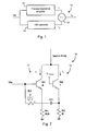
- Fig. 1 illustrates one embodiment of the invention, an IM3-compensated amplifier 10, formed on a single chip.
- the transconductance amplifier 12 portion is conventional and may be part of a mixer in a demodulator of a wireless receiver.
- An IM3 canceller 14 circuit generates a current I 2 that substantially offsets or reduces the IM3 products of interest in the current I 1 generated by the amplifier 12.
- a subtractor 16 represents the current generated by the IM3 canceller 14 being subtracted from the current generated by the amplifier 12, although the IM3 canceller 14 itself may provide the offsetting correction to the output of the amplifier 12 without the use of a separate subtractor.
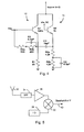
- Fig. 2 illustrates an embodiment of the circuit of Fig. 1 .
- Various other embodiments are envisioned.
- the transconductance amplifier 12 comprise a first NPN bipolar transistor Q1 having its base coupled to an RF input voltage (Vin), such as a modulated RF signal received by a cellular telephone.
- Vin is generated by high-pass filtering an incoming RF signal (to filter out its DC component) and combining the filtered AC signal with a separately generated DC bias voltage for setting the quiescent current of transistor Q1. In this manner, the bias voltage can be optimized.
- the emitter area is given by A. It is assumed that the area A is proportional to the transconductance of the transistor for a given Vbe.
- the emitter may be coupled to ground via a first resistor R1.
- the current I 1 is assumed to contain IM3 distortion.
- the IM3 cancellation circuit 14 comprises a second NPN bipolar transistor Q2 having its base coupled to the DC component of Vin (the DC bias voltage). Accordingly, the base voltage of transistor Q2 is relatively stable. Its emitter is coupled to ground via a second resistor R2. The emitter is also coupled to Vin via an AC coupling capacitor C1 (blocks DC) in series with a third resistor R3. Accordingly, the variable conductance of the second NPN bipolar transistor Q2 is determined by the change in its emitter voltage (corresponding to the AC component of Vin). For negative-going Vin signals, the second NPN bipolar transistor Q2 conducts more current and, for positive-going Vin signals, the second NPN bipolar transistor Q2 conducts less current. This is opposite to the conductance of the first NPN bipolar transistor Q1.
- the conductance of the IM3 cancellation circuit 14 is 180 degrees out of phase with the conductance of the transconductance amplifier 12, enabling the cancellation (or reduction) of the IM3 components in the combined output current I 1 +I 2 (the compensated current) or enabling the cancellation of the IM3 components anywhere in the receiver.
- resistor R2 is R
- the emitter area of the transistor Q2 is 1
- the emitter area of the transistor Q1 is A
- the value of resistor R1 is approximately R/A.
- the ratio of the current through transistor Q1 to the current through transistor Q2 will be approximately the ratio of their respective areas, in this case A/1.
- the relative values of the resistors R1 and R2 equalize the change in emitter voltage for both transistors with changes in current through the respective transistors even though the area A of transistor Q1 may be many times greater than the area of transistor Q2. In this way, the current densities through transistors Q1 and Q2 are approximately equal, which allows tracking the input power over a large range.
- the area of transistor Q1 should be much greater than the area of transistor Q2 in order to maintain high transconductance (see Eq. 11) and improve noise performance.
- the value of resistor R3 is approximately R / A 3 .
- Capacitor C1 and resistors R2 and R3 form a high pass filter, whose cut-off frequency must be significantly below the IM3 frequency of interest in order for the circuit to accurately cancel the IM3 products.
- the values of the various components are determined during simulation and calibration, where, during simulation, a two-tone input is applied to the circuit and the IM3 products to be cancelled are calculated. The values of the various components are then adjusted during simulation or during fabrication to cancel out the calculated or measured IM3 products of interest.
- the two tones may represent the RF carrier and an LO leakage frequency, or may represent RF interference from any external source, or may represent other tones generated in the system.
- the IM3 canceller 14 offsets the target IM3 distortion current generated by the transconductance amplifier 12 or by any other source. If the IM3 distortion is generated during a mixing process, where the RF compensated current is mixed with a local oscillator current to demodulate Vin, the components in the IM3 canceller 14 can be selected to compensate for the downstream IM3 distortion by the mixer. The selection of component values may correct for any IM3 distortion occurring anywhere in the receiver.
- the IM3 canceller 14 Since the IM3 canceller 14 is formed along with the transconductance amplifier 12 on the same chip, the cancellation tracks variations in the transconductance amplifier 12 due to temperature and process variations.
- Fig. 3 shows the output current (I 2 ) of the IM3 canceller 14, the output current (I 1 ) of the transconductance amplifier 12, the total output current (I OUT ), and the 3 rd derivatives of I 1 , I 2 , and I OUT , using values given in Fig. 4 .
- I OUT has a minimal IM3 coefficient. Also, for this signal amplitude range, the IM3 coefficient for a positive-going signal approximately cancels the IM3 coefficient for a negative-going signal.
- the AC voltages at R1 and R3 are approximately equal, assuming the AC frequency is well above the cut-off frequency of the capacitor-resistor filter.
- the optimum value for resistor R3 will typically be in the range of R/10 to R. Detailed simulation of the circuit performance including parasitics is usually necessary to arrive at the optimum value for resistor R3.
- Fig. 2 When the circuit of Fig. 2 is operated at above certain high frequencies, the gain of the "smaller” transistor Q2 lowers more than the gain of the "bigger” transistor Q1, since some AC device parasitics scale less than A if transistor Q1 is optimized for high frequencies. Accordingly, better cancellation of IM3 products can be obtained over a larger bandwidth by using some bypass capacitors across the resistor R3 and the resistor R2. This increases the responsiveness of the IM3 canceller 14.
- Fig 4 shows a specific implementation with such compensation applied to the circuit in Fig. 2 .
- Resistor R3 and resistor R2 are split into R3a, R3b, R2a, and R2b, respectively, and a portion of the resistance has a high frequency bypass path through capacitors C2 and C3 to lower the effective impedances at high frequencies.
- Capacitor C1 provides the AC coupling, assuming the Vin frequencies of interest are much higher than the cut-off frequency provided by the resulting capacitor-resistor high pass filter. Examples of values of the resistors (in ohms), values of capacitors, and relative areas of the transistors are given.
- Vin would be applied to the gate of a first n-channel MOSFET in a transconductance amplifier, and the DC component of Vin would be applied to the gate of a second n-channel MOSFET.
- the AC component of Vin would be applied to the source of the second MOSFET so that the IM3 canceller generates an IM3 current that is opposite to the IM3 distortion generated by the transconductance amplifier (the IM3 compensation may also compensate for other distortions).
- the respective areas (A) would then refer to the gate widths of the MOSFETs.
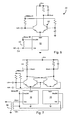
- Fig. 5 illustrates the inventive circuit incorporated in a mixer 30 of a demodulator in an RF receiver, such as a cellular telephone.
- An antenna 32 receives the RF signal.
- a bandpass filter 34 passes the frequency of interest to a low noise amplifier 36.
- the mixer 30 mixes the RF signal with a local oscillator (LO) 38 signal to generate a down-converted signal 40 at the output.
- the signal 40 may be baseband or an intermediate frequency (IF). All components, except the antenna 32, may be formed on the same chip.
- Fig. 6 illustrates the mixer 30 of Fig. 5 in more detail, showing the IM3-compensated amplifier 10 as the "tail" current source for the mixer 30.
- Vout is the demodulated output of the mixer 30.
- a DC bias voltage Vbias,LO is generated for biasing the differential pair of transistors 50 at an optimal quiescent current.
- Vbias,LO is 3 volts.
- An incoming RF signal is high-pass filtered by capacitor C4, and a separate DC bias voltage Vbias,RF is generated for DC biasing the transistor Q1 ( Fig. 2 ).
- An inductor 52 couples Vbias,RF to the base of transistor Q1. The voltages are combined to generate Vin for applying to the base of transistor Q1 ( Fig. 2 ).
- Vbias,RF is 1.5 volts.
- the Vbias(RF) is also applied to the base of transistor Q2 ( Fig. 2 ).
- the compensated current Iout compensates for IM3 distortion generated during the mixing of the RF and LO signals.
- the circuit may be designed to compensate for IM3 distortion caused at any stage in the receiver or due to RF interference.
- Fig. 7 illustrates a doubly-balanced mixer implementation, showing the IM3-compensated amplifier 10 as the "tail" current source for each side of the mixer.
- Vout+ and Vout- are the balanced outputs of the mixer.
- Vin+ and Vin- are generated using a balun transformer 56 with a center-tap for the Vin,DC bias.
- IM3 canceller the cancellation will typically not be perfect due to the actual circuit differing from simulation, due to the attenuation vs. frequency effects of the filter, and due to other real-world limitations. Accordingly, an actual IM3 canceller 14 will substantially offset (rather than perfectly cancel) the IM3 distortion output by the transconductance amplifier 12. In practical real-world implementations, the actual circuit can improve the IP3 by up to 5 to 10dB
Landscapes
- Engineering & Computer Science (AREA)
- Power Engineering (AREA)
- Physics & Mathematics (AREA)
- Nonlinear Science (AREA)
- Amplifiers (AREA)
Abstract
Description
- This invention relates to a cancellation circuit for third order intermodulation (IM3) products in an RF transconductor, such as used in mixers or amplifiers in wireless receivers.
- A transconductor may be a transconductance amplifier that generates a change in output current with a change in input voltage. An actual transconductance amplifier, such as in a mixer of an RF receiver, produces some distortion, such as generating second and third harmonics of the fundamental frequency, generating frequency-mixed signals, and generating intermodulation products. For example, a typical transconductance amplifier receiving sine waves f1 and f2 will output the following signals, having various magnitudes. The second and third order signals are output due to distortion:
TERM OUTPUT FREQUENCY linear fundamental f1, f2 2nd order 2nd harmonic 2f1, 2f 23rd order 3rd harmonic 3f1, 3f2 2nd order frequency mixing (f2-f1), (f2+f1) 3rd order 3rd order intermod. products (2f2-f1), (2f1-f2) - The output current of a non-ideal transconductance amplifier can be described by the following power series, limited to the third order, where transconductance (represented by the coefficient an) is defined as the change in output current (i(t))with a change in input voltage (v(t)):

where the dc quiescent current is represented by a 0, the linear transconductance is represented by a 1, the second-order non-linearity is represented by a 2, and the third-order non-linearity is represented by a 3. The third order intermodulation (IM3) products are a3v(t)3. Transconductance is also referred to herein as gm. - The IM3 products are the most problematic in some situations since they may occur near a fundamental frequency and may be difficult to filter out.
- Transconductance amplifiers are typically used in mixers forming part of a demodulator of an RF receiver.
- There are many types of prior art IM3 cancellers. Some predistort the input voltage to compensate for the IM3 distortion. Some require differential signals to generate an IM3 correction. RF signals in the gigahertz range may be difficult to accurately convert to differential signals and may require transformers that add expense and real estate. Various drawbacks exist with the prior art IM3 cancellers, including imprecision due to process and temperature variations, the difficulty in creating differential signals at high frequencies due to component limitations, complexity, real estate requirements, and other issues.
- What is needed is a simpler IM3 canceller that can operate at high frequencies, such as at gigahertz frequencies for cell phones, and is self-adjusting for process and temperature variations.
- An IM3 cancellation circuit is formed in parallel with a transconductance amplifier. The amplifier may be part of a mixer in a wireless RF receiver or other component in an RF receiver.
- The transconductance amplifier may comprise a first NPN bipolar transistor having its base directly coupled to an RF input voltage (Vin), such as a modulated RF signal received by a cellular telephone. The emitter may be coupled to ground via a first resistor R1.
- In one embodiment, Vin is generated by high-pass filtering an incoming RF signal and combining the filtered AC signal with a separately generated DC bias voltage for setting the quiescent current of transistor Q1.
- The IM3 cancellation circuit comprises a second NPN bipolar transistor having its base coupled to the DC component of Vin (a DC bias voltage). Accordingly, the base voltage is relatively stable. Its emitter is coupled to ground via a second resistor R2. The emitter is also coupled to Vin via an AC coupling capacitor C1 (blocks DC) in series with a third resistor R3. Accordingly, the variable conductance of the second NPN bipolar transistor is determined by the change in its emitter voltage (corresponding to the AC component of Vin), while the variable conductance of the first NPN bipolar transistor is determined by the change in its base-emitter voltage (corresponding to the AC component of Vin). Therefore, the current through the IM3 cancellation circuit changes opposite to the current of the transconductance amplifier, and the IM3 cancellation circuit can be designed to cancel IM3 components in the combined output current or offset IM3 components generated anywhere in the receiver.
- The IM3 cancellation circuit may also be designed, by proper selection of its component values, to cancel IM3 distortion generated by a demodulator containing the circuit. Such IM3 distortion may be other than any distortion generated by the transconductance amplifier or generated in combination with distortion by the transconductance amplifier.
- The values of the resistors, capacitor, and areas of the transistors are calculated to offset the target IM3 products during simulation and/or calibration of the circuit.
- Since the IM3 cancelling circuit is formed along with the transconductance amplifier on the same chip, the cancellation tracks variations in the transconductance amplifier due to temperature and process variations.
- In one embodiment, the compensated output current is mixed with a local oscillator current to demodulate Vin to generate a baseband or intermediate frequency (IF) signal (Vout) in a receiver. The IM3 cancellation circuit is thus designed to offset any IM3 distortion (from whatever source) in the demodulated Vin signal.
- Various other embodiments are described. For example, the circuit may be implemented using MOSFETs instead of bipolar transistors.
- Preferred embodiments of the present invention will now be described, by way of example only, with reference to the accompanying drawings, of which:
-
Fig. 1 is a high level diagram illustrating the transconductance amplifier and the IM3 canceller connected in parallel. -
Fig. 2 is a transistor-level diagram of the transconductance amplifier and the IM3 canceller connected in parallel, in accordance with one embodiment of the invention. -
Fig. 3 illustrates the derivation of the IM3 products for a particular output current during calibration of the circuit ofFig. 2 in order to set the values of components needed to cancel out the target IM3 products. -
Fig. 4 illustrates a variation of the circuit ofFig. 2 that enables the circuit to have a wider bandwidth for accurate operation. -
Fig. 5 illustrates an arrangement according to the invention as part of a mixer in a wireless receiver, such as a cell phone. -
Fig. 6 illustrates the mixer ofFig. 5 in more detail, showing the IM3-compensated amplifier as the "tail" current source for the mixer. -
Fig. 7 illustrates a doubly-balanced mixer implementation. - Elements that are the same or equivalent are labeled with the same numeral.
-
Fig. 1 illustrates one embodiment of the invention, an IM3-compensatedamplifier 10, formed on a single chip. Thetransconductance amplifier 12 portion is conventional and may be part of a mixer in a demodulator of a wireless receiver. AnIM3 canceller 14 circuit generates a current I2 that substantially offsets or reduces the IM3 products of interest in the current I1 generated by theamplifier 12. Asubtractor 16 represents the current generated by theIM3 canceller 14 being subtracted from the current generated by theamplifier 12, although theIM3 canceller 14 itself may provide the offsetting correction to the output of theamplifier 12 without the use of a separate subtractor. -
Fig. 2 illustrates an embodiment of the circuit ofFig. 1 . Various other embodiments are envisioned. - The
transconductance amplifier 12 comprise a first NPN bipolar transistor Q1 having its base coupled to an RF input voltage (Vin), such as a modulated RF signal received by a cellular telephone. In one embodiment, Vin is generated by high-pass filtering an incoming RF signal (to filter out its DC component) and combining the filtered AC signal with a separately generated DC bias voltage for setting the quiescent current of transistor Q1. In this manner, the bias voltage can be optimized. - The emitter area is given by A. It is assumed that the area A is proportional to the transconductance of the transistor for a given Vbe. The emitter may be coupled to ground via a first resistor R1. The current I1 is assumed to contain IM3 distortion.
- The
IM3 cancellation circuit 14 comprises a second NPN bipolar transistor Q2 having its base coupled to the DC component of Vin (the DC bias voltage). Accordingly, the base voltage of transistor Q2 is relatively stable. Its emitter is coupled to ground via a second resistor R2. The emitter is also coupled to Vin via an AC coupling capacitor C1 (blocks DC) in series with a third resistor R3. Accordingly, the variable conductance of the second NPN bipolar transistor Q2 is determined by the change in its emitter voltage (corresponding to the AC component of Vin). For negative-going Vin signals, the second NPN bipolar transistor Q2 conducts more current and, for positive-going Vin signals, the second NPN bipolar transistor Q2 conducts less current. This is opposite to the conductance of the first NPN bipolar transistor Q1. Therefore, the conductance of theIM3 cancellation circuit 14 is 180 degrees out of phase with the conductance of thetransconductance amplifier 12, enabling the cancellation (or reduction) of the IM3 components in the combined output current I1+I2 (the compensated current) or enabling the cancellation of the IM3 components anywhere in the receiver. - Assume the value of resistor R2 is R, the emitter area of the transistor Q2 is 1, the emitter area of the transistor Q1 is A, and the value of resistor R1 is approximately R/A. Given the same voltage difference between the base and emitters of the two transistors, the ratio of the current through transistor Q1 to the current through transistor Q2 will be approximately the ratio of their respective areas, in this case A/1. The relative values of the resistors R1 and R2 equalize the change in emitter voltage for both transistors with changes in current through the respective transistors even though the area A of transistor Q1 may be many times greater than the area of transistor Q2. In this way, the current densities through transistors Q1 and Q2 are approximately equal, which allows tracking the input power over a large range. The area of transistor Q1 should be much greater than the area of transistor Q2 in order to maintain high transconductance (see Eq. 11) and improve noise performance. The value of resistor R3 is approximately

- Capacitor C1 and resistors R2 and R3 form a high pass filter, whose cut-off frequency must be significantly below the IM3 frequency of interest in order for the circuit to accurately cancel the IM3 products. The values of the various components are determined during simulation and calibration, where, during simulation, a two-tone input is applied to the circuit and the IM3 products to be cancelled are calculated. The values of the various components are then adjusted during simulation or during fabrication to cancel out the calculated or measured IM3 products of interest. The two tones may represent the RF carrier and an LO leakage frequency, or may represent RF interference from any external source, or may represent other tones generated in the system.
- In this way, the
IM3 canceller 14 offsets the target IM3 distortion current generated by thetransconductance amplifier 12 or by any other source. If the IM3 distortion is generated during a mixing process, where the RF compensated current is mixed with a local oscillator current to demodulate Vin, the components in theIM3 canceller 14 can be selected to compensate for the downstream IM3 distortion by the mixer. The selection of component values may correct for any IM3 distortion occurring anywhere in the receiver. - Since the
IM3 canceller 14 is formed along with thetransconductance amplifier 12 on the same chip, the cancellation tracks variations in thetransconductance amplifier 12 due to temperature and process variations. - More detail regarding calculation of the IM3 products follow.
- A two-tone input voltage signal can be represented by:

- The transconductor output current in Eq.1 can then be written as:

- The IM3 products are found at angular frequencies of 2ω 2 - ω 1 and 2ω 1 - ω 2. Assuming a 3 << a 1, the ratio of the coefficient of the linear product to the coefficient of the IM3 products can be used as a linearity figure of merit or the third-order intercept point, IP3:

- To maximize the IP3, it is clear from Eq.4 that the coefficient a 3 must be minimized or made equal to zero. In order to isolate the coefficient a 3 , the 3rd derivative of the output current can be taken.
Fig. 3 shows the output current (I2) of theIM3 canceller 14, the output current (I1) of thetransconductance amplifier 12, the total output current (IOUT), and the 3rd derivatives of I1, I2, and IOUT, using values given inFig. 4 . - By inspection, it can be seen that, for signal amplitudes less than about 0.15V, IOUT has a minimal IM3 coefficient. Also, for this signal amplitude range, the IM3 coefficient for a positive-going signal approximately cancels the IM3 coefficient for a negative-going signal.
- Referring to
Fig. 2 , in all cases, the AC voltages at R1 and R3 are approximately equal, assuming the AC frequency is well above the cut-off frequency of the capacitor-resistor filter. - For the case of A=1, R3=R and R1=R and if R>>1/gmQ2, we can write the two output currents I1 and I2, considering just the linear and 3rd order terms, as:

- Then, the IM3-affected output IOUT = I 1 + I 2 = 0 . Note that a 3 in Eq.5 and Eq.6 are substantially equal since both Q1 and Q2 run at the same current densities, due to the relationship of R1 and R2 to the respective areas of the transistors Q1 and Q2.
- For the case of A>1, R3=R, and if R>>1/gmQ2, the currents can be written:

- Then,

- If, in the desired case, A>1, R>>1/gmQ2, and


- Then, the 3rd-order terms desirably cancel and the output current can be written:

- Accordingly, the relationships of the values of the components in the circuit of
Fig. 2 needed to completely cancel the IM3 products of interest have been shown. Note that the signal voltage at the emitter of transistor Q2 is multiplied by approximately


- When the circuit of
Fig. 2 is operated at above certain high frequencies, the gain of the "smaller" transistor Q2 lowers more than the gain of the "bigger" transistor Q1, since some AC device parasitics scale less than A if transistor Q1 is optimized for high frequencies. Accordingly, better cancellation of IM3 products can be obtained over a larger bandwidth by using some bypass capacitors across the resistor R3 and the resistor R2. This increases the responsiveness of theIM3 canceller 14.Fig 4 shows a specific implementation with such compensation applied to the circuit inFig. 2 . Resistor R3 and resistor R2 are split into R3a, R3b, R2a, and R2b, respectively, and a portion of the resistance has a high frequency bypass path through capacitors C2 and C3 to lower the effective impedances at high frequencies. Capacitor C1 provides the AC coupling, assuming the Vin frequencies of interest are much higher than the cut-off frequency provided by the resulting capacitor-resistor high pass filter. Examples of values of the resistors (in ohms), values of capacitors, and relative areas of the transistors are given. - Other embodiments are envisioned, such as an all MOSFET circuit. In a MOSFET implementation of
Fig. 2 , Vin would be applied to the gate of a first n-channel MOSFET in a transconductance amplifier, and the DC component of Vin would be applied to the gate of a second n-channel MOSFET. The AC component of Vin would be applied to the source of the second MOSFET so that the IM3 canceller generates an IM3 current that is opposite to the IM3 distortion generated by the transconductance amplifier (the IM3 compensation may also compensate for other distortions). The respective areas (A) would then refer to the gate widths of the MOSFETs. -
Fig. 5 illustrates the inventive circuit incorporated in amixer 30 of a demodulator in an RF receiver, such as a cellular telephone. Anantenna 32 receives the RF signal. Abandpass filter 34 passes the frequency of interest to alow noise amplifier 36. Themixer 30 mixes the RF signal with a local oscillator (LO) 38 signal to generate a down-convertedsignal 40 at the output. Thesignal 40 may be baseband or an intermediate frequency (IF). All components, except theantenna 32, may be formed on the same chip. -
Fig. 6 illustrates themixer 30 ofFig. 5 in more detail, showing the IM3-compensatedamplifier 10 as the "tail" current source for themixer 30. Vout is the demodulated output of themixer 30. A DC bias voltage Vbias,LO is generated for biasing the differential pair oftransistors 50 at an optimal quiescent current. In one embodiment, Vbias,LO is 3 volts. - An incoming RF signal is high-pass filtered by capacitor C4, and a separate DC bias voltage Vbias,RF is generated for DC biasing the transistor Q1 (
Fig. 2 ). Aninductor 52 couples Vbias,RF to the base of transistor Q1. The voltages are combined to generate Vin for applying to the base of transistor Q1 (Fig. 2 ). In one embodiment, Vbias,RF is 1.5 volts. The Vbias(RF) is also applied to the base of transistor Q2 (Fig. 2 ). The compensated current Iout compensates for IM3 distortion generated during the mixing of the RF and LO signals. The circuit may be designed to compensate for IM3 distortion caused at any stage in the receiver or due to RF interference. -
Fig. 7 illustrates a doubly-balanced mixer implementation, showing the IM3-compensatedamplifier 10 as the "tail" current source for each side of the mixer. Vout+ and Vout- are the balanced outputs of the mixer. Vin+ and Vin- are generated using abalun transformer 56 with a center-tap for the Vin,DC bias. - Although the term "IM3 canceller" has been used herein, the cancellation will typically not be perfect due to the actual circuit differing from simulation, due to the attenuation vs. frequency effects of the filter, and due to other real-world limitations. Accordingly, an
actual IM3 canceller 14 will substantially offset (rather than perfectly cancel) the IM3 distortion output by thetransconductance amplifier 12. In practical real-world implementations, the actual circuit can improve the IP3 by up to 5 to 10dB - While particular embodiments of the present invention have been shown and described, it will be obvious to those skilled in the art that changes and modifications may be made without departing from this invention in its broader aspects and, therefore, the appended claims are to encompass within their scope all such changes and modifications that are within the true scope of this invention. For example, the features and modifications of the embodiments described may be combined or interchanged as desired.
- The disclosures in United States patent application no.
13/323,753
Claims (20)
- A circuit that reduces third-order intermodulation (IM3) product distortion, the circuit comprising:a transconductance amplifier comprising a first transistor configured to conduct a first current related to a voltage difference between a first terminal and a second terminal of the first transistor, the first terminal being coupled to receive an RF input voltage (Vin) having a DC component and an AC component, the first transistor also having third terminal for conducting the first current controlled by Vin; andan IM3 canceller circuit comprising a second transistor configured to conduct a second current related to a voltage difference between a fourth terminal and a fifth terminal of the second transistor, the fourth terminal being coupled to substantially receive only the DC component of Vin, the fifth terminal coupled to substantially receive only the AC component of Vin, the second transistor also having a sixth terminal for conducting the second current controlled by the AC component such that an increase in the first current conducted by first transistor occurs during a decrease in the second current conducted by the second transistor, and vice versa,wherein the third terminal of the first transistor is coupled to the sixth terminal of the second transistor such that the second current at least partially offsets IM3 distortion.
- The circuit of Claim 1 further comprising a capacitor coupled to filter Vin to generate the AC component.
- The circuit of Claim 1 or 2 wherein the first transistor has a first size (A1) and wherein the second transistor has a smaller second size (A2), wherein a ratio of currents through the first transistor and the second transistor is approximately A1/A2 given the same voltage difference between the first terminal and the second terminal of the first transistor, and between the fourth terminal and the fifth terminal of the second transistor.
- The circuit of Claim 3 further comprising:a first resistor, having a first value, coupled to the second terminal of the first transistor; anda second resistor, having a second value, coupled to the fifth terminal of the second transistor, the second value being larger than the first value;wherein the second value of the second resistor is R and the first value of the first resistor is approximately R/(A1/A2).
- The circuit of Claim 4 further comprising:a capacitor coupled to filter Vin to generate the AC component; anda third resistor coupled in series with the capacitor between Vin and the fifth terminal of the second transistor, the third resistor having a third value related to A1/A2 for adjusting a voltage at the fifth terminal in response to the AC component to cause the second current to at least partially offset IM3 distortion.
- The circuit of Claim 5 wherein the second resistor comprises at least two resistors in series, the circuit further comprising a bypass capacitor in parallel with one of the resistors in series.
- The circuit of Claim 5 wherein the third resistor comprises at least two resistors in series, the circuit further comprising a bypass capacitor in parallel with one of the resistors in series.
- The circuit of any preceding Claim wherein the first transistor and the second transistor are bipolar transistors, wherein the first terminal is a base of the first transistor, the second terminal is an emitter of the first transistor, the third terminal is a collector of the first transistor, the fourth terminal is a base of the second transistor, the fifth terminal is an emitter of the second transistor, and the sixth terminal is a collector of the second transistor.
- The circuit of any preceding Claim wherein the combined first current and second current is a current generated in a demodulator for an RF signal.
- The circuit of any of Claims 1 to 8 wherein the combined first current and second current is a current generated in a mixer for an RF signal.
- The circuit of any preceding Claim wherein the second current at least partially offsets IM3 distortion in the first current.
- The circuit of any of claims 1 to 10 wherein the second current at least partially offsets IM3 distortion generated in a demodulator containing the circuit.
- A method of reducing third-order intermodulation (IM3) product distortion, the method comprising:providing a transconductance amplifier comprising a first transistor configured to conduct a first current related to a voltage difference between a first terminal and a second terminal of the first transistor;applying an RF input voltage (Vin) to the first terminal, Vin having a DC component and an AC component, the first transistor also having third terminal for conducting the first current controlled by Vin;providing an IM3 canceller circuit comprising a second transistor configured to conduct a second current related to a voltage difference between a fourth terminal and a fifth terminal of the second transistor;applying substantially only the DC component of Vin to the fourth terminal; andapplying substantially only the AC component of Vin to the fifth terminal, the second transistor also having a sixth terminal for conducting the second current controlled by the AC component such that an increase in the first current conducted by first transistor occurs during a decrease in the second current conducted by the second transistor, and vice versa,wherein the third terminal of the first transistor is coupled to the sixth terminal of the second transistor such that the second current at least partially offsets IM3 distortion.
- The method of Claim 13 or 14 further comprising high-pass filtering Vin by a capacitor to generate the AC component.
- The method of Claim 13 wherein the first transistor has first size (A1) and wherein the second transistor has a smaller second size (A2), wherein a ratio of currents through the first transistor and the second transistor is approximately A1/A2 given the same voltage difference between the first terminal and the second terminal of the first transistor, and between the fourth terminal and the fifth terminal of the second transistor.
- The method of Claim 15 further comprising high-pass filtering Vin by a capacitor to generate the AC component, the IM3 canceller circuit further comprising:a resistor coupled in series with the capacitor between Vin and the fifth terminal of the second transistor, the third resistor having a third value related to A1/A2 for adjusting a voltage at the fifth terminal in response to the AC component to cause the second current to at least partially offset IM3 distortion.
- The method of any of Claim 13 to 16 wherein the first transistor and the second transistor are bipolar transistors, wherein the first terminal is a base of the first transistor, the second terminal is an emitter of the first transistor, the third terminal is a collector of the first transistor, the fourth terminal is a base of the second transistor, the fifth terminal is an emitter of the second transistor, and the sixth terminal is a collector of the second transistor.
- The method of any of Claims 13 to 17 further comprising:combining the first current and second current to provide a compensated current in a demodulator for Vin; andmixing the compensated current with a local oscillator current to demodulate Vin.
- The method of any of Claims 13 to 18 wherein the second current at least partially offsets IM3 distortion in the first current.
- The method of any of Claims 13 to 18 wherein the second current at least partially offsets IM3 distortion generated in the demodulator.
Applications Claiming Priority (1)
| Application Number | Priority Date | Filing Date | Title |
|---|---|---|---|
| US13/323,753 US8373503B1 (en) | 2011-12-12 | 2011-12-12 | Third order intermodulation cancellation for RF transconductors |
Publications (3)
| Publication Number | Publication Date |
|---|---|
| EP2605402A2 true EP2605402A2 (en) | 2013-06-19 |
| EP2605402A3 EP2605402A3 (en) | 2015-06-17 |
| EP2605402B1 EP2605402B1 (en) | 2016-04-06 |
Family
ID=47355824
Family Applications (1)
| Application Number | Title | Priority Date | Filing Date |
|---|---|---|---|
| EP12193843.5A Active EP2605402B1 (en) | 2011-12-12 | 2012-11-22 | Third order intermodulation cancellation for RF transconductors |
Country Status (2)
| Country | Link |
|---|---|
| US (1) | US8373503B1 (en) |
| EP (1) | EP2605402B1 (en) |
Families Citing this family (3)
| Publication number | Priority date | Publication date | Assignee | Title |
|---|---|---|---|---|
| JP6263936B2 (en) * | 2013-10-03 | 2018-01-24 | 富士通株式会社 | amplifier |
| CN109643973B (en) * | 2016-08-25 | 2022-05-13 | 华为技术有限公司 | Integrated amplifier |
| US10374554B2 (en) * | 2017-12-27 | 2019-08-06 | Qualcomm Incorporated | Differential amplifier with complementary unit structure |
Family Cites Families (11)
| Publication number | Priority date | Publication date | Assignee | Title |
|---|---|---|---|---|
| US6684065B2 (en) * | 1999-12-20 | 2004-01-27 | Broadcom Corporation | Variable gain amplifier for low voltage applications |
| FR2823921B1 (en) * | 2001-04-20 | 2003-10-31 | St Microelectronics Sa | TRANSCONDUCTANCE STAGE AND WIRELESS COMMUNICATION DEVICE PROVIDED WITH SUCH A STAGE |
| JP4004018B2 (en) * | 2001-06-29 | 2007-11-07 | 株式会社東芝 | Frequency converter and radio communication apparatus using the same |
| CA2467184A1 (en) | 2004-05-12 | 2005-11-12 | Sirific Wireless Corporation | Im3 cancellation using cmos elements |
| KR100631973B1 (en) * | 2005-03-02 | 2006-10-11 | 삼성전기주식회사 | Variable gain broadband amplifier |
| US7902925B2 (en) * | 2005-08-02 | 2011-03-08 | Qualcomm, Incorporated | Amplifier with active post-distortion linearization |
| US8035447B2 (en) * | 2007-08-21 | 2011-10-11 | Qualcomm, Incorporated | Active circuits with load linearization |
| US8131245B2 (en) * | 2007-09-13 | 2012-03-06 | Cambridge Silicon Radio Limited | Mixer for downconversion of RF signals |
| US7944298B2 (en) * | 2007-12-18 | 2011-05-17 | Qualcomm, Incorporated | Low noise and low input capacitance differential MDS LNA |
| US7696828B2 (en) * | 2008-01-04 | 2010-04-13 | Qualcomm, Incorporated | Multi-linearity mode LNA having a deboost current path |
| US7936220B2 (en) * | 2008-12-12 | 2011-05-03 | Qualcomm, Incorporated | Techniques for improving amplifier linearity |
-
2011
- 2011-12-12 US US13/323,753 patent/US8373503B1/en not_active Expired - Fee Related
-
2012
- 2012-11-22 EP EP12193843.5A patent/EP2605402B1/en active Active
Non-Patent Citations (1)
| Title |
|---|
| None |
Also Published As
| Publication number | Publication date |
|---|---|
| US8373503B1 (en) | 2013-02-12 |
| EP2605402A3 (en) | 2015-06-17 |
| EP2605402B1 (en) | 2016-04-06 |
Similar Documents
| Publication | Publication Date | Title |
|---|---|---|
| CN101647196B (en) | Differential amplifier with active post-distortion linearization | |
| US7099646B1 (en) | Signal mixer having a single-ended input and a differential output | |
| US5945878A (en) | Single-ended to differential converter | |
| US6943628B2 (en) | Methods and apparatus for substantially reducing nonlinear distortion | |
| KR101599592B1 (en) | Reducing non-linearities in a differential receiver path prior to a mixer using calibration | |
| CN101273525B (en) | Amplifier with active post-distortion linearization | |
| Lou et al. | A linearization technique for RF receiver front-end using second-order-intermodulation injection | |
| US20080032646A1 (en) | Circuits | |
| US20090219094A1 (en) | Differential amplifier circuit and frequency mixer for improving linearity | |
| US8169266B2 (en) | Mixer circuits and methods | |
| US11018640B2 (en) | Differential amplifier, corresponding integrated circuit, system, instrumentation amplifier and method | |
| WO2009123583A1 (en) | Tunable rf bandpass transconductance amplifier | |
| US11171609B2 (en) | Systems and methods for detecting local oscillator leakage and image tone in I/Q mixer based transceivers | |
| EP2137828B1 (en) | An rf input transconductor stage | |
| US20070037544A1 (en) | Integrated RF circuits | |
| US6992519B2 (en) | Method and apparatus providing cancellation of second order intermodulation distortion and enhancement of second order intercept point (IIP2) in common source and common emitter transconductance circuits | |
| US7642816B2 (en) | Transconductor | |
| EP2605402B1 (en) | Third order intermodulation cancellation for RF transconductors | |
| CN110945781B (en) | Single balanced voltage mode passive mixer with symmetric sideband gain | |
| US8536926B2 (en) | Gilbert mixer | |
| JP2007537631A (en) | Third-order modulation cancellation variable circuit | |
| US8483646B2 (en) | Second order intermodulation canceller | |
| CN111917382B (en) | Low-noise amplifier based on active inductor with noise elimination | |
| FI20216009A1 (en) | Voltage-controlled current amplifiers with asymmetric input and differential output and their applications | |
| CN113364438A (en) | High-linearity intermediate frequency buffer circuit and buffer |
Legal Events
| Date | Code | Title | Description |
|---|---|---|---|
| PUAI | Public reference made under article 153(3) epc to a published international application that has entered the european phase |
Free format text: ORIGINAL CODE: 0009012 |
|
| AK | Designated contracting states |
Kind code of ref document: A2 Designated state(s): AL AT BE BG CH CY CZ DE DK EE ES FI FR GB GR HR HU IE IS IT LI LT LU LV MC MK MT NL NO PL PT RO RS SE SI SK SM TR |
|
| AX | Request for extension of the european patent |
Extension state: BA ME |
|
| PUAL | Search report despatched |
Free format text: ORIGINAL CODE: 0009013 |
|
| AK | Designated contracting states |
Kind code of ref document: A3 Designated state(s): AL AT BE BG CH CY CZ DE DK EE ES FI FR GB GR HR HU IE IS IT LI LT LU LV MC MK MT NL NO PL PT RO RS SE SI SK SM TR |
|
| AX | Request for extension of the european patent |
Extension state: BA ME |
|
| RIC1 | Information provided on ipc code assigned before grant |
Ipc: H03F 3/19 20060101ALI20150508BHEP Ipc: H03F 3/45 20060101ALI20150508BHEP Ipc: H03F 1/32 20060101AFI20150508BHEP |
|
| 17P | Request for examination filed |
Effective date: 20150603 |
|
| RBV | Designated contracting states (corrected) |
Designated state(s): AL AT BE BG CH CY CZ DE DK EE ES FI FR GB GR HR HU IE IS IT LI LT LU LV MC MK MT NL NO PL PT RO RS SE SI SK SM TR |
|
| GRAP | Despatch of communication of intention to grant a patent |
Free format text: ORIGINAL CODE: EPIDOSNIGR1 |
|
| INTG | Intention to grant announced |
Effective date: 20151012 |
|
| GRAS | Grant fee paid |
Free format text: ORIGINAL CODE: EPIDOSNIGR3 |
|
| GRAA | (expected) grant |
Free format text: ORIGINAL CODE: 0009210 |
|
| AK | Designated contracting states |
Kind code of ref document: B1 Designated state(s): AL AT BE BG CH CY CZ DE DK EE ES FI FR GB GR HR HU IE IS IT LI LT LU LV MC MK MT NL NO PL PT RO RS SE SI SK SM TR |
|
| REG | Reference to a national code |
Ref country code: GB Ref legal event code: FG4D |
|
| REG | Reference to a national code |
Ref country code: AT Ref legal event code: REF Ref document number: 788747 Country of ref document: AT Kind code of ref document: T Effective date: 20160415 Ref country code: CH Ref legal event code: EP |
|
| REG | Reference to a national code |
Ref country code: IE Ref legal event code: FG4D |
|
| REG | Reference to a national code |
Ref country code: DE Ref legal event code: R096 Ref document number: 602012016552 Country of ref document: DE |
|
| REG | Reference to a national code |
Ref country code: NL Ref legal event code: FP |
|
| REG | Reference to a national code |
Ref country code: LT Ref legal event code: MG4D |
|
| REG | Reference to a national code |
Ref country code: AT Ref legal event code: MK05 Ref document number: 788747 Country of ref document: AT Kind code of ref document: T Effective date: 20160406 |
|
| PG25 | Lapsed in a contracting state [announced via postgrant information from national office to epo] |
Ref country code: PL Free format text: LAPSE BECAUSE OF FAILURE TO SUBMIT A TRANSLATION OF THE DESCRIPTION OR TO PAY THE FEE WITHIN THE PRESCRIBED TIME-LIMIT Effective date: 20160406 Ref country code: FI Free format text: LAPSE BECAUSE OF FAILURE TO SUBMIT A TRANSLATION OF THE DESCRIPTION OR TO PAY THE FEE WITHIN THE PRESCRIBED TIME-LIMIT Effective date: 20160406 Ref country code: IS Free format text: LAPSE BECAUSE OF FAILURE TO SUBMIT A TRANSLATION OF THE DESCRIPTION OR TO PAY THE FEE WITHIN THE PRESCRIBED TIME-LIMIT Effective date: 20160806 Ref country code: LT Free format text: LAPSE BECAUSE OF FAILURE TO SUBMIT A TRANSLATION OF THE DESCRIPTION OR TO PAY THE FEE WITHIN THE PRESCRIBED TIME-LIMIT Effective date: 20160406 Ref country code: NO Free format text: LAPSE BECAUSE OF FAILURE TO SUBMIT A TRANSLATION OF THE DESCRIPTION OR TO PAY THE FEE WITHIN THE PRESCRIBED TIME-LIMIT Effective date: 20160706 |
|
| REG | Reference to a national code |
Ref country code: FR Ref legal event code: PLFP Year of fee payment: 5 |
|
| PG25 | Lapsed in a contracting state [announced via postgrant information from national office to epo] |
Ref country code: AT Free format text: LAPSE BECAUSE OF FAILURE TO SUBMIT A TRANSLATION OF THE DESCRIPTION OR TO PAY THE FEE WITHIN THE PRESCRIBED TIME-LIMIT Effective date: 20160406 Ref country code: GR Free format text: LAPSE BECAUSE OF FAILURE TO SUBMIT A TRANSLATION OF THE DESCRIPTION OR TO PAY THE FEE WITHIN THE PRESCRIBED TIME-LIMIT Effective date: 20160707 Ref country code: LV Free format text: LAPSE BECAUSE OF FAILURE TO SUBMIT A TRANSLATION OF THE DESCRIPTION OR TO PAY THE FEE WITHIN THE PRESCRIBED TIME-LIMIT Effective date: 20160406 Ref country code: ES Free format text: LAPSE BECAUSE OF FAILURE TO SUBMIT A TRANSLATION OF THE DESCRIPTION OR TO PAY THE FEE WITHIN THE PRESCRIBED TIME-LIMIT Effective date: 20160406 Ref country code: PT Free format text: LAPSE BECAUSE OF FAILURE TO SUBMIT A TRANSLATION OF THE DESCRIPTION OR TO PAY THE FEE WITHIN THE PRESCRIBED TIME-LIMIT Effective date: 20160808 Ref country code: SE Free format text: LAPSE BECAUSE OF FAILURE TO SUBMIT A TRANSLATION OF THE DESCRIPTION OR TO PAY THE FEE WITHIN THE PRESCRIBED TIME-LIMIT Effective date: 20160406 Ref country code: HR Free format text: LAPSE BECAUSE OF FAILURE TO SUBMIT A TRANSLATION OF THE DESCRIPTION OR TO PAY THE FEE WITHIN THE PRESCRIBED TIME-LIMIT Effective date: 20160406 Ref country code: RS Free format text: LAPSE BECAUSE OF FAILURE TO SUBMIT A TRANSLATION OF THE DESCRIPTION OR TO PAY THE FEE WITHIN THE PRESCRIBED TIME-LIMIT Effective date: 20160406 |
|
| PG25 | Lapsed in a contracting state [announced via postgrant information from national office to epo] |
Ref country code: BE Free format text: LAPSE BECAUSE OF FAILURE TO SUBMIT A TRANSLATION OF THE DESCRIPTION OR TO PAY THE FEE WITHIN THE PRESCRIBED TIME-LIMIT Effective date: 20160406 |
|
| REG | Reference to a national code |
Ref country code: DE Ref legal event code: R097 Ref document number: 602012016552 Country of ref document: DE |
|
| PG25 | Lapsed in a contracting state [announced via postgrant information from national office to epo] |
Ref country code: CZ Free format text: LAPSE BECAUSE OF FAILURE TO SUBMIT A TRANSLATION OF THE DESCRIPTION OR TO PAY THE FEE WITHIN THE PRESCRIBED TIME-LIMIT Effective date: 20160406 Ref country code: SK Free format text: LAPSE BECAUSE OF FAILURE TO SUBMIT A TRANSLATION OF THE DESCRIPTION OR TO PAY THE FEE WITHIN THE PRESCRIBED TIME-LIMIT Effective date: 20160406 Ref country code: EE Free format text: LAPSE BECAUSE OF FAILURE TO SUBMIT A TRANSLATION OF THE DESCRIPTION OR TO PAY THE FEE WITHIN THE PRESCRIBED TIME-LIMIT Effective date: 20160406 Ref country code: RO Free format text: LAPSE BECAUSE OF FAILURE TO SUBMIT A TRANSLATION OF THE DESCRIPTION OR TO PAY THE FEE WITHIN THE PRESCRIBED TIME-LIMIT Effective date: 20160406 Ref country code: DK Free format text: LAPSE BECAUSE OF FAILURE TO SUBMIT A TRANSLATION OF THE DESCRIPTION OR TO PAY THE FEE WITHIN THE PRESCRIBED TIME-LIMIT Effective date: 20160406 |
|
| PLBE | No opposition filed within time limit |
Free format text: ORIGINAL CODE: 0009261 |
|
| STAA | Information on the status of an ep patent application or granted ep patent |
Free format text: STATUS: NO OPPOSITION FILED WITHIN TIME LIMIT |
|
| PG25 | Lapsed in a contracting state [announced via postgrant information from national office to epo] |
Ref country code: SM Free format text: LAPSE BECAUSE OF FAILURE TO SUBMIT A TRANSLATION OF THE DESCRIPTION OR TO PAY THE FEE WITHIN THE PRESCRIBED TIME-LIMIT Effective date: 20160406 |
|
| 26N | No opposition filed |
Effective date: 20170110 |
|
| PG25 | Lapsed in a contracting state [announced via postgrant information from national office to epo] |
Ref country code: SI Free format text: LAPSE BECAUSE OF FAILURE TO SUBMIT A TRANSLATION OF THE DESCRIPTION OR TO PAY THE FEE WITHIN THE PRESCRIBED TIME-LIMIT Effective date: 20160406 |
|
| REG | Reference to a national code |
Ref country code: CH Ref legal event code: PL |
|
| PG25 | Lapsed in a contracting state [announced via postgrant information from national office to epo] |
Ref country code: LI Free format text: LAPSE BECAUSE OF NON-PAYMENT OF DUE FEES Effective date: 20161130 Ref country code: CH Free format text: LAPSE BECAUSE OF NON-PAYMENT OF DUE FEES Effective date: 20161130 |
|
| REG | Reference to a national code |
Ref country code: IE Ref legal event code: MM4A |
|
| PG25 | Lapsed in a contracting state [announced via postgrant information from national office to epo] |
Ref country code: LU Free format text: LAPSE BECAUSE OF NON-PAYMENT OF DUE FEES Effective date: 20161130 |
|
| REG | Reference to a national code |
Ref country code: FR Ref legal event code: PLFP Year of fee payment: 6 |
|
| PG25 | Lapsed in a contracting state [announced via postgrant information from national office to epo] |
Ref country code: IE Free format text: LAPSE BECAUSE OF NON-PAYMENT OF DUE FEES Effective date: 20161122 |
|
| PG25 | Lapsed in a contracting state [announced via postgrant information from national office to epo] |
Ref country code: CY Free format text: LAPSE BECAUSE OF FAILURE TO SUBMIT A TRANSLATION OF THE DESCRIPTION OR TO PAY THE FEE WITHIN THE PRESCRIBED TIME-LIMIT Effective date: 20160406 Ref country code: HU Free format text: LAPSE BECAUSE OF FAILURE TO SUBMIT A TRANSLATION OF THE DESCRIPTION OR TO PAY THE FEE WITHIN THE PRESCRIBED TIME-LIMIT; INVALID AB INITIO Effective date: 20121122 |
|
| PG25 | Lapsed in a contracting state [announced via postgrant information from national office to epo] |
Ref country code: MK Free format text: LAPSE BECAUSE OF FAILURE TO SUBMIT A TRANSLATION OF THE DESCRIPTION OR TO PAY THE FEE WITHIN THE PRESCRIBED TIME-LIMIT Effective date: 20160406 Ref country code: MC Free format text: LAPSE BECAUSE OF FAILURE TO SUBMIT A TRANSLATION OF THE DESCRIPTION OR TO PAY THE FEE WITHIN THE PRESCRIBED TIME-LIMIT Effective date: 20160406 Ref country code: TR Free format text: LAPSE BECAUSE OF FAILURE TO SUBMIT A TRANSLATION OF THE DESCRIPTION OR TO PAY THE FEE WITHIN THE PRESCRIBED TIME-LIMIT Effective date: 20160406 |
|
| PG25 | Lapsed in a contracting state [announced via postgrant information from national office to epo] |
Ref country code: BG Free format text: LAPSE BECAUSE OF FAILURE TO SUBMIT A TRANSLATION OF THE DESCRIPTION OR TO PAY THE FEE WITHIN THE PRESCRIBED TIME-LIMIT Effective date: 20160406 |
|
| PG25 | Lapsed in a contracting state [announced via postgrant information from national office to epo] |
Ref country code: MT Free format text: LAPSE BECAUSE OF NON-PAYMENT OF DUE FEES Effective date: 20161122 |
|
| REG | Reference to a national code |
Ref country code: FR Ref legal event code: PLFP Year of fee payment: 7 |
|
| PG25 | Lapsed in a contracting state [announced via postgrant information from national office to epo] |
Ref country code: AL Free format text: LAPSE BECAUSE OF FAILURE TO SUBMIT A TRANSLATION OF THE DESCRIPTION OR TO PAY THE FEE WITHIN THE PRESCRIBED TIME-LIMIT Effective date: 20160406 |
|
| REG | Reference to a national code |
Ref country code: DE Ref legal event code: R082 Ref document number: 602012016552 Country of ref document: DE Representative=s name: MUELLER-BORE & PARTNER PATENTANWAELTE PARTG MB, DE Ref country code: DE Ref legal event code: R081 Ref document number: 602012016552 Country of ref document: DE Owner name: ANALOG DEVICES INTERNATIONAL UNLIMITED COMPANY, IE Free format text: FORMER OWNER: LINEAR TECHNOLOGY CORPORATION, MILPITAS, CALIF., US Ref country code: DE Ref legal event code: R082 Ref document number: 602012016552 Country of ref document: DE Representative=s name: WITHERS & ROGERS LLP, DE |
|
| REG | Reference to a national code |
Ref country code: DE Ref legal event code: R082 Ref document number: 602012016552 Country of ref document: DE Representative=s name: WITHERS & ROGERS LLP, DE |
|
| REG | Reference to a national code |
Ref country code: GB Ref legal event code: 732E Free format text: REGISTERED BETWEEN 20211125 AND 20211201 |
|
| REG | Reference to a national code |
Ref country code: NL Ref legal event code: PD Owner name: ANALOG DEVICES INTERNATIONAL UNLIMITED COMPANY; IE Free format text: DETAILS ASSIGNMENT: CHANGE OF OWNER(S), ASSIGNMENT; FORMER OWNER NAME: LINEAR TECHNOLOGY LLC Effective date: 20211216 |
|
| PGFP | Annual fee paid to national office [announced via postgrant information from national office to epo] |
Ref country code: IT Payment date: 20211025 Year of fee payment: 10 |
|
| PG25 | Lapsed in a contracting state [announced via postgrant information from national office to epo] |
Ref country code: IT Free format text: LAPSE BECAUSE OF NON-PAYMENT OF DUE FEES Effective date: 20221122 |
|
| PGFP | Annual fee paid to national office [announced via postgrant information from national office to epo] |
Ref country code: NL Payment date: 20231020 Year of fee payment: 12 |
|
| PGFP | Annual fee paid to national office [announced via postgrant information from national office to epo] |
Ref country code: GB Payment date: 20231019 Year of fee payment: 12 |
|
| PGFP | Annual fee paid to national office [announced via postgrant information from national office to epo] |
Ref country code: FR Payment date: 20231019 Year of fee payment: 12 |
|
| REG | Reference to a national code |
Ref country code: NL Ref legal event code: MM Effective date: 20241201 |
|
| GBPC | Gb: european patent ceased through non-payment of renewal fee |
Effective date: 20241122 |
|
| PG25 | Lapsed in a contracting state [announced via postgrant information from national office to epo] |
Ref country code: NL Free format text: LAPSE BECAUSE OF NON-PAYMENT OF DUE FEES Effective date: 20241201 |
|
| PG25 | Lapsed in a contracting state [announced via postgrant information from national office to epo] |
Ref country code: GB Free format text: LAPSE BECAUSE OF NON-PAYMENT OF DUE FEES Effective date: 20241122 |
|
| PG25 | Lapsed in a contracting state [announced via postgrant information from national office to epo] |
Ref country code: FR Free format text: LAPSE BECAUSE OF NON-PAYMENT OF DUE FEES Effective date: 20241130 |
|
| PGFP | Annual fee paid to national office [announced via postgrant information from national office to epo] |
Ref country code: DE Payment date: 20251022 Year of fee payment: 14 |